

LG XC62, XCS62F Service manual

MICRO Hi-Fi SYSTEM
SERVICE MANUAL
MODEL : XC62 (XCS62F)
CAUTION
BEFORE SERVICING THE UNIT, READ THE “SAFETY PRECAUTIONS”
IN THIS MANUAL
.
MODEL : XC62 (XCS62F)
SERVICE MANUAL
P/NO : AFN33894992 APRIL, 2007
http://biz.lgservice.com

CONTENTS
SECTION 1
GENERAL
SERVICING PRECAUTIONS ......................................1-2
• NOTES REGARDING HANDLING OF THE PICK-UP
•
NOTES REGARDING COMPACT DISC PLAYER REPAIRS
ESD PRECAUTIONS ...................................................1-4
LOCATION OF USERS CONTROLS .........................1-5
SPECIFICATIONS ........................................................1-7
SECTION 2
EXPLODED VIEWS
CABINET EXPLODED VIEW......................................2-1
TAPE DECK MECHANISM (SINGLE DECK)
EXPLODED VIEW ........................................................2-3
CD MECHANISM EXPLODED VIEW.........................2-5
SPEAKER EXPLODED VIEW ....................................2-7
MODEL : XCS62F ....................................................2-7
PACKING ACCESSORY VIEW...................................2-9
SECTION 3
AUDIO PART ELECTRICAL
AUDIO ELECTRICAL
TROUBLESHOOTING GUIDE....................................3-1
1. POWER (SMPS) ................................................3-1
2. MICOM PART CHECK I ....................................3-4
3. MICOM PART CHECK II ...................................3-5
4. IC103(KS4CD21CS) CHECK............................3-6
5. FLD DISPLAY CHECK ......................................3-7
6. PWM MODULATION PART CHECK................3-8
7. POWER AMP PART CHECK............................3-9
8. AUX FUNCTION CHECK................................3-10
9. TUNER FUNCTION CHECK...........................3-11
10. TAPE FUNCTION CHECK ..............................3-12
11. TAPE PLAY PART CHECK..............................3-13
12. TAPE REC PART CHECK...............................3-14
13. PORTABLE IN FUNCTION CHECK...............3-15
INTERNAL BLOCK DIAGRAM OF ICs...................3-15
1. AK5358..............................................................3-16
2. BU4052 .............................................................3-16
3. HA12237F.........................................................3-17
4. LC78692NW .....................................................3-18
5. PS9829B...........................................................3-18
6. PT6324..............................................................3-19
7. STR-W6253......................................................3-19
8. TAS5142 ...........................................................3-20
9. U1739EJ2V1UD00/KF2_E ..............................3-21
10. UTC MC4580....................................................3-22
WIRING DIAGRAM ....................................................3-24
BLOCK DIAGRAM.....................................................3-26
1. SMPS BLOCK DIAGRAM...............................3-26
2. MAIN & FRONT BLOCK DIAGRAM ..............3-28
SCHEMATIC DIAGRAMS .........................................3-30
1. SMPS SCHEMATIC DIAGRAM.......................3-30
2. MAIN SCHEMATIC DIAGRAM ........................3-32
3. AMP SCHEMATIC DIAGRAM..........................3-34
4. DECK SCHEMATIC DIAGRAM .......................3-36
5. FRONT SCHEMATIC DIAGRAM.....................3-38
PRINTED CIRCUIT BOARD DIAGRAMS ...............3-40
1. MAIN P.C.BOARD ............................................3-40
2. SMPS P.C.BOARD ..........................................3-44
3. FRONT P.C.BOARD ........................................3-46
SECTION 4
CD PART ELECTRICAL
CD ELECTRICAL TROUBLESHOOTING GUIDE....4-1
1. CD PART TROUBLESHOOTING.....................4-1
2. USB PART TROUBLESHOOTING...................4-9
WAVEFORMS OF MAJOR CHECK POINT............4-10
1. MICOM INTERFACE WAVEFORM.................4-10
2. SLED DRIVE AND MOTOR WAVEFORM......4-11
3. FOCUS DRIVE AND MOTOR
WAVEFORM ......................................................4-11
4. SPINDLE DRIVE AND MOTOR
WAVEFORM......................................................4-12
5. TRACK DRIVE AND MOTOR
WAVEFORM......................................................4-12
6. RF, FOCUS AND TRACKING
ERROR WAVEFORM .......................................4-12
SCHEMATIC DIAGRAMS .........................................4-13
1. CD SCHEMATIC DIAGRAM ...........................4-13
2. USB SCHEMATIC DIAGRAM.........................4-15
PRINTED CIRCUIT BOARD DIAGRAM..................4-17
CD P.C.BOARD ....................................................4-17
SECTION 5
REPLACEMENT PARTS LIST
........5-1
1-1
SECTION 1 GENERAL
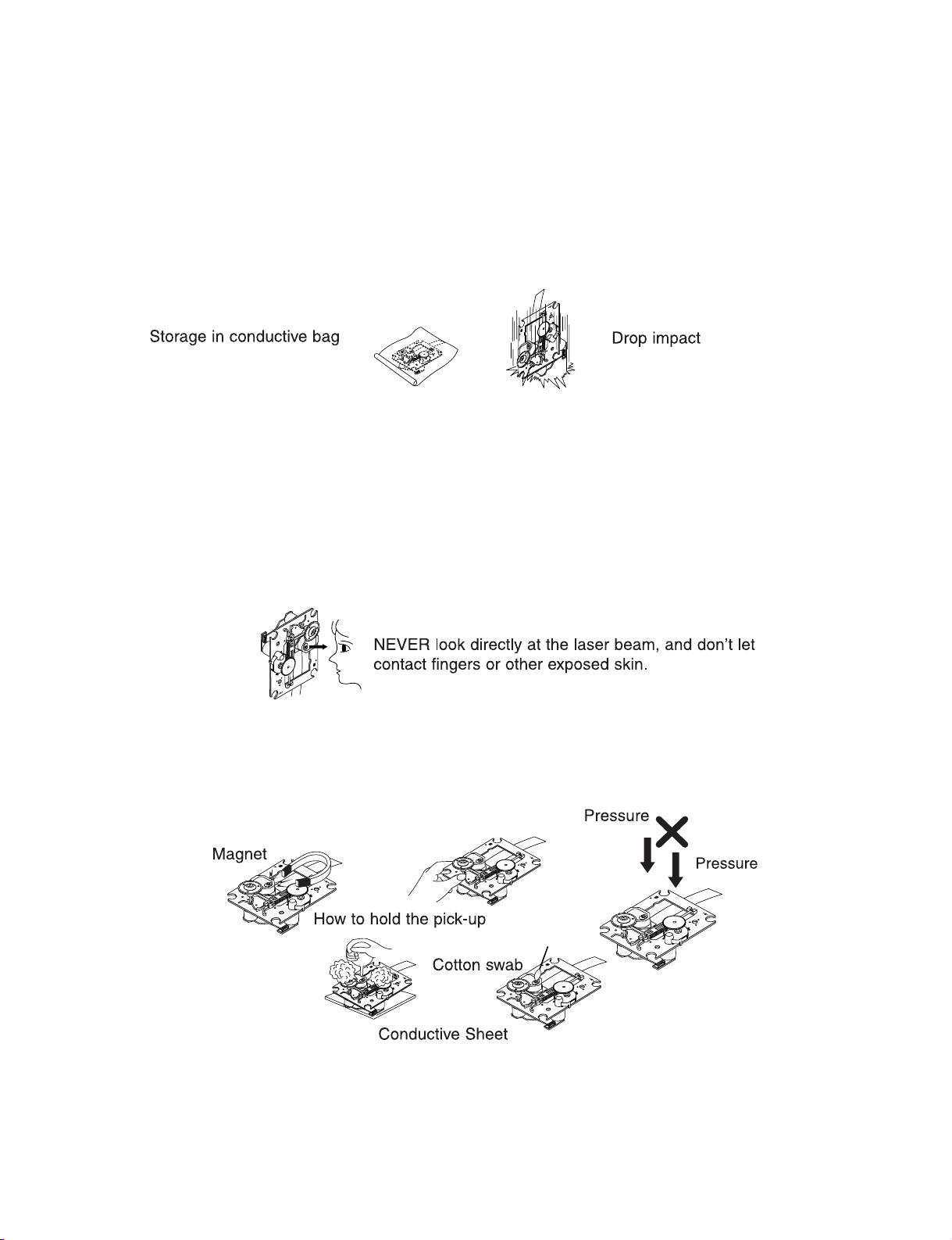
SERVICING PRECAUTIONS
NOTES REGARDING HANDLING OF THE PICK-UP
1. Notes for transport and storage
1) The pick-up should always be left in its conductive bag until immediately prior to use.
2) The pick-up should never be subjected to external pressure or impact.
2. Repair notes
1) The pick-up incorporates a strong magnet, and so should never be brought close to magnetic materials.
2) The pick-up should always be handled correctly and carefully, taking care to avoid external pressure and
impact. If it is subjected to strong pressure or impact, the result may be an operational malfunction and/or
damage to the printed-circuit board.
3) Each and every pick-up is already individually adjusted to a high degree of precision, and for that reason
the adjustment point and installation screws should absolutely never be touched.
4) Laser beams may damage the eyes!
Absolutely never permit laser beams to enter the eyes!
Also NEVER switch ON the power to the laser output part (lens, etc.) of the pick-up if it is damaged.
5) Cleaning the lens surface
If there is dust on the lens surface, the dust should be cleaned away by using an air bush (such as used
for camera lens). The lens is held by a delicate spring. When cleaning the lens surface, therefore, a cotton
swab should be used, taking care not to distort this.
6) Never attempt to disassemble the pick-up.
Spring by excess pressure. If the lens is extremely dirty, apply isopropyl alcohol to the cotton swab. (Do not
use any other liquid cleaners, because they will damage the lens.) Take care not to use too much of this
alcohol on the swab, and do not allow the alcohol to get inside the pick-up.
1-2

NOTES REGARDING COMPACT DISC PLAYER REPAIRS
1. Preparations
1) Compact disc players incorporate a great many ICs as well as the pick-up (laser diode). These components
are sensitive to, and easily affected by, static electricity. If such static electricity is high voltage, components
can be damaged, and for that reason components should be handled with care.
2) The pick-up is composed of many optical components and other high-precision components. Care must be
taken, therefore, to avoid repair or storage where the temperature of humidity is high, where strong
magnetism is present, or where there is excessive dust.
2. Notes for repair
1) Before replacing a component part, first disconnect the power supply lead wire from the unit
2) All equipment, measuring instruments and tools must be grounded.
3) The workbench should be covered with a conductive sheet and grounded.
When removing the laser pick-up from its conductive bag, do not place the pick-up on the bag. (This is
because there is the possibility of damage by static electricity.)
4) To prevent AC leakage, the metal part of the soldering iron should be grounded.
5) Workers should be grounded by an armband (1MΩ)
6) Care should be taken not to permit the laser pick-up to come in contact with clothing, in order to prevent
static electricity changes in the clothing to escape from the armband.
7) The laser beam from the pick-up should NEVER be directly facing the eyes or bare skin.
CLEARING MALFUNCTION
You can reset your unit to initial status if malfunction occur(button malfunction, display, etc.).
Using a pointed good conductor(such as driver), simply short the RESET jump wire on the inside of
the volume knob for more than 3 seconds.
If you reset your unit, you must reenter all its settings(stations, clock, timer)
NOTE: 1. To operate the RESET jump wire, pull the volume rotary knob and release it.
2. If you wish to operate the RESET jump wire, it is necessary to unplug the power cord.
1-3
ESD PRECAUTIONS
Electrostatically Sensitive Devices (ESD)
Some semiconductor (solid state) devices can be damaged easily by static electricity. Such components
commonly are called electrostatically sensitive devices (ESD). Examples of typical ESD devices are
integrated circuits and some field-effect transistors and semiconductor chip components. The following
techniques should be used to help reduce the incidence of component damage caused by static electricity.
1. Immediately before handling any semiconductor component or semiconductor-equipped assembly, drain
off any electrostatic charge on your body by touching a know earth ground. Alternatively, obtain and
wear a commercially available discharging wrist strap device, which should be removed for potential
shock reasons prior to applying power to the unit under test.
2. After removing an electrical assembly equipped with ESD devices, place the assembly on a conductive
surface such as aluminum foil, to prevent electrostatic charge buildup or exposure of the assembly.
3. Use only a grounded-tip soldering iron to solder or unsolder ESD devices.
4. Use only an anti-static solder removal device. Some solder removal devices not classified as "anti-static"
can generate electrical charges sufficient to damage ESD devices.
5. Do not use freon-propelled chemicals These can generate electrical charges sufficient to damage ESD
devices.
6. Do not remove a replacement ESD device from its protective package until immediately before you are
ready to install it. (Most replacement ESD devices are packaged with leads electrically shorted together
by conductive foam, aluminum foil or comparable conductive materials).
7. Immediately before removing the protective material from the leads of a replacement ESD device, touch
the protective material to the chassis or circuit assembly into which the device will by installed.
CAUTION : BE SURE NO POWER IS APPLIED TO THE CHASSIS OR CIRCUIT, AND OBSERVE ALL
OTHER SAFETY PRECAUTIONS.
8. Minimize bodily motions when handing unpackaged replacement ESD devices. (Otherwise harmless
motion such as the brushing together of your clothes fabric or the lifting of your foot from a carpeted floor
can generate static electricity sufficient to damage an ESD device).
[CAUTION. GRAPHIC SYMBOLS]
THE LIGHTNING FLASH WITH ARROWHEAD SYMBOL. WITHIN AN EQUILATERAL
TRIANGLE, IS INTENDED TO ALERT THE SERVICE PERSONNEL TO THE PRESENCE
OF UNINSULATED "DANGEROUS VOLTAGE" THAT MAY BE OF SUFFICIENT
MAGNITUDE TO CONSTITUTE A RISK OF ELECTRIC SHOCK.
THE EXCLAMATION POINT WITHIN AN EQUILATERAL TRIANGLE IS INTENED TO
ALERT THE SERVICE PERSONNEL TO THE PRESENCE OF IMPORTANT SAFETY
INFORMATION IN SERVICE LITERATURE.
1-4
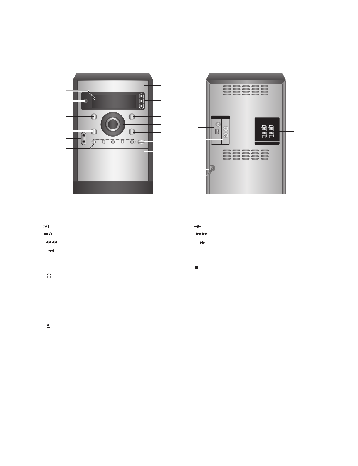
LOCATION OF USERS CONTROLS
FRONT / BACK PANEL
1
2
3
4
5
6
1. DISPLAY WINDOW
2. (POWER)
3. PLAY(PAUSE)
4. • (CD SKIP/SEARCH)
(FAST REWIND PLAY)
• TUNE.-
5. • PORT.IN jack
• (Headphone jack) : ø3.5mm
6. • FUNCTION
(FM, AM, CD, USB, AUX, PORTABLE, TAPE)
• XDSS plus
• PLAY MODE/ST./MONO
• CD SYNC
• CD OPEN (DEMO)
13
12
11
10
9
8
7
14
17
15
16
7. PUSH EJECT position
8. (USB connector)
9. • (CD SKIP/SEARCH)
(FAST FORWARD PLAY)
• TUNE.+
10.VOLUME CONTROL KNOB
11. STO P
12.• TIMER
• CLOCK
• SET (RDS - OPTIONAL)
13.DISC TRAY
14.AM/FM ANTENNA TERMINAL
15.AUX IN (AUXILIARY INPUT) connector
16.POWER IN (POWER CORD)
17.SPEAKER TERMINAL
1-5
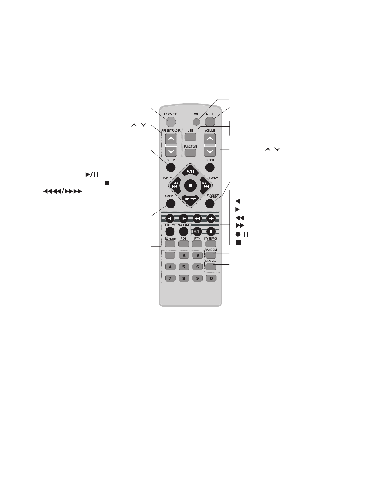
REMOTE CONTROL
POWER
DIMMER
MUTE
PRESET/FOLDER( )
/
SLEEP
CD FUNCTION
(PLAY/PAUSE) •
(CD STOP) •
(CD SKIP/SEARCH) •
TUN.-/+ •
REPEAT •
D.SKIP
XTS Pro •
XDSS plus •
EQ master •
RDS (Radio Data System) FUNCTION
RDS : OPTIONAL •
PTY : OPTIONAL •
PTY SEARCH : OPTIONAL •
• USB
• FUNCTION
VOLUME ( )
/
CLOCK
PROGRAM/MEMO
TAPE FUNCTION
• (BACKWARD PLAY)
• (FORWARD PLAY)
• (FAST REWIND PLAY)
• (FAST FORWARD PLAY)
• / (RECORD/RECORD PAUSE)
• (TAPE STOP)
RANDOM
MP3 Info
(MP3/WMA file information display)
NUMERIC
1-6

SPECIFICATIONS
• GENERAL
Power supply Refer to the back panel of the unit.
Power consumption Refer to the back panel of the unit.
Net Weight 3.4kg
External dimensions (WxHxD) 170 x 243 x 282mm
• TUNER
FM Tuning Range 87.5 ~ 108.0MHz or 65 ~ 74MHz, 87.5 ~ 108.0MHz
Intermediate Frequency 10.7MHz
Signal to Noise Ratio 60/55dB (MONO/STEREO)
Frequency Response 50 ~ 10000Hz
AM Tuning Range 522 ~ 1620kHz or 520 ~ 1720kHz
Intermediate Frequency 450kHz
Signal to Noise Ratio 30dB
Frequency Response 140 ~ 1800Hz
• AMPLIFIER
Output Power 30W + 30W
T.H.D 0.5%
Frequency Response 40 ~ 20000Hz
Signal-to-noise ratio 75dB
• CD
Frequency response 40 ~ 20000Hz
Signal-to-noise ratio 75dB
Dynamic range 75dB
• CASSETTE TAPE PLAYER
Tape Speed 3000 ± 3% (MTT-111. NORMAL-SPEED)
Wow Flutter 0.25% (MTT-111, JIS-WTD)
F.F/REW Time 120sec (C-60)
Frequency Response 250 ~ 8000Hz
Signal to Noise Ratio 43dB
Channel Separation 45dB (P/B) / 45dB (R/P)
Erase Ratio 50dB (MTT-5511)
• SPEAKERS
Type 1Way 1Speaker
Impedance 4Ω
Frequency Response 75 ~ 17000Hz
Sound Pressure Level 83dB/W (1m)
Rated Input Power 30W
Max. Input Power 60W
Net Dimensions (WxHxD) 144 x 243 x 171mm
Net Weight (1EA) 1.47kg
1-7

MEMO
1-8
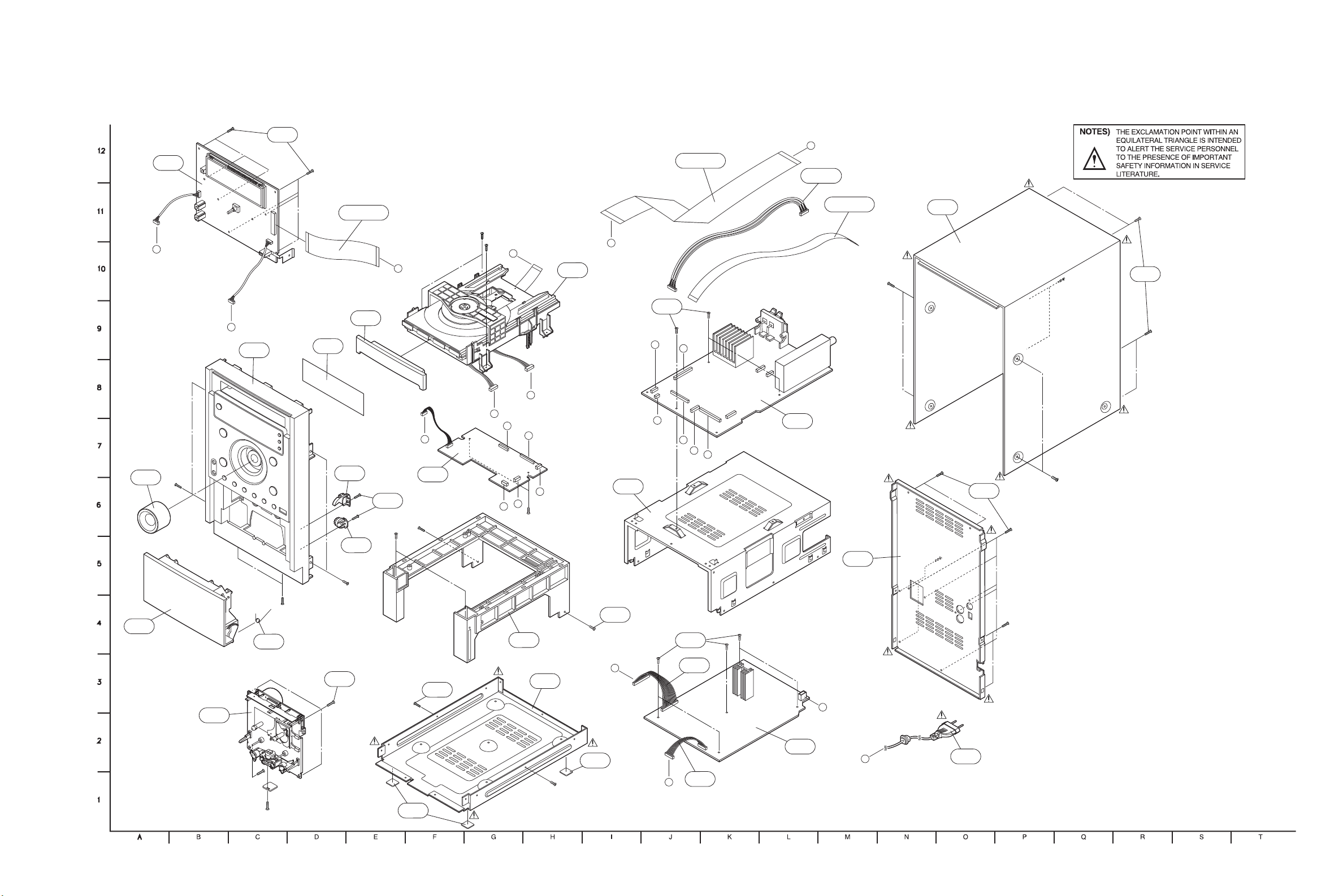
A
C
D
H
I
A
B
K
E
J
F
L
B
C
E
G
L
D
F
H
I
J
K
G
454
A26
A46
264
263
266
A43
250
254
252
253
255
259
454
A47
CN2
CN1
305
454
454
454
A00
267
290
256
A52
CD
SMPS
FRONT
MAIN
CABLE3
CABLE2
CABLE1
CN201
454
290
454
454
454
SECTION 2 EXPLODED VIEWS
257
258
CABINET EXPLODED VIEW
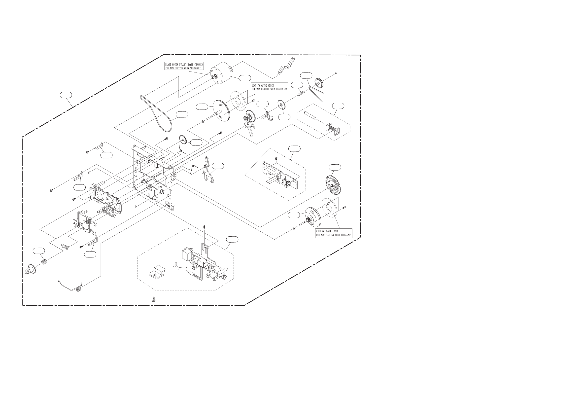
TAPE DECK MECHANISM (SINGLE DECK) EXPLODED VIEW
A00
009
003
001
007
037
015
006
017
020
019
022
018
A01
023
025
011
A02
009
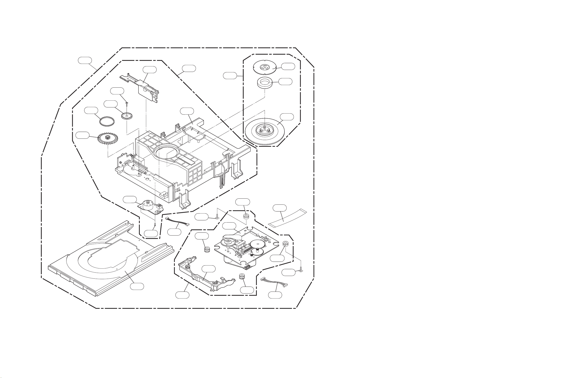
CD MECHANISM (CDM-330) EXPLODED VIEW
A26
018
439
014
013
017
A02
020
001
A01
002
003
015
026
431
016
A03
432
012
019
012A
010
036
012A
432
012
037
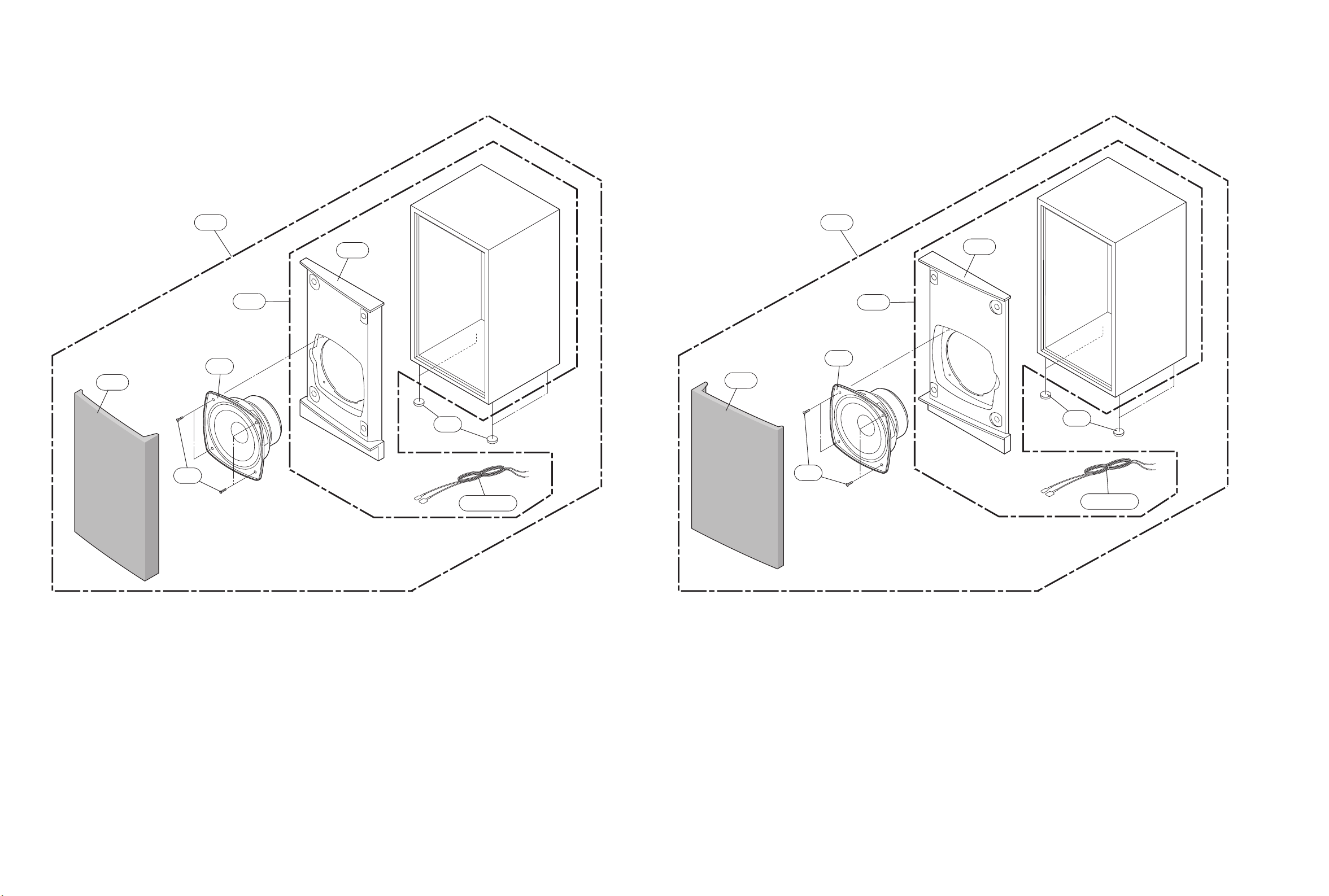
SPEAKER EXPLODED VIEW
MODEL : XCS62F
850L
851
A80
852
A80L
853L
854
WIRE80
A81
853R
A80R
852
850R
854
851
WIRE80
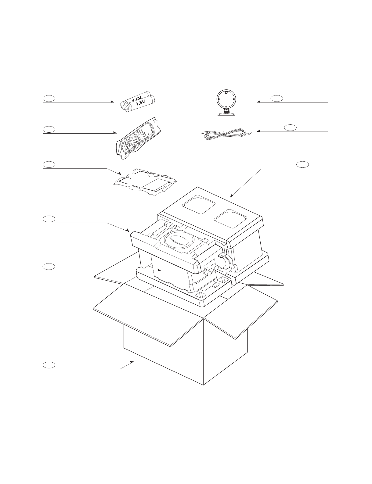
PACKING ACCESSORY VIEW
808 Battery
900 Remote Control
801 Instruction Ass'y
803 Packing
804 Bag
824 Antenna Loop (AM)
825 Antenna (FM)
803 Packing
802 Box
2-9
SECTION 3 AUDIO PART ELECTRICAL
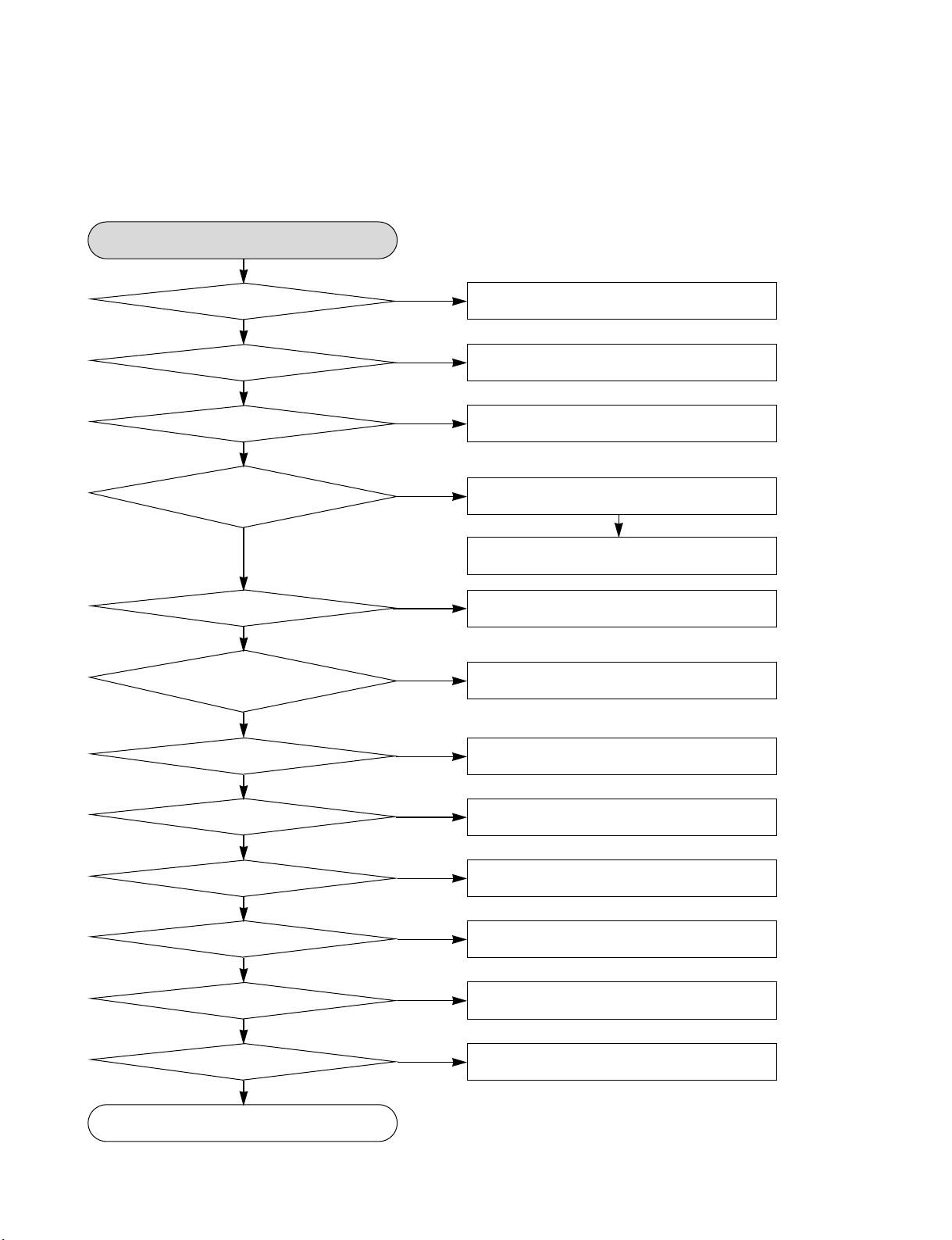
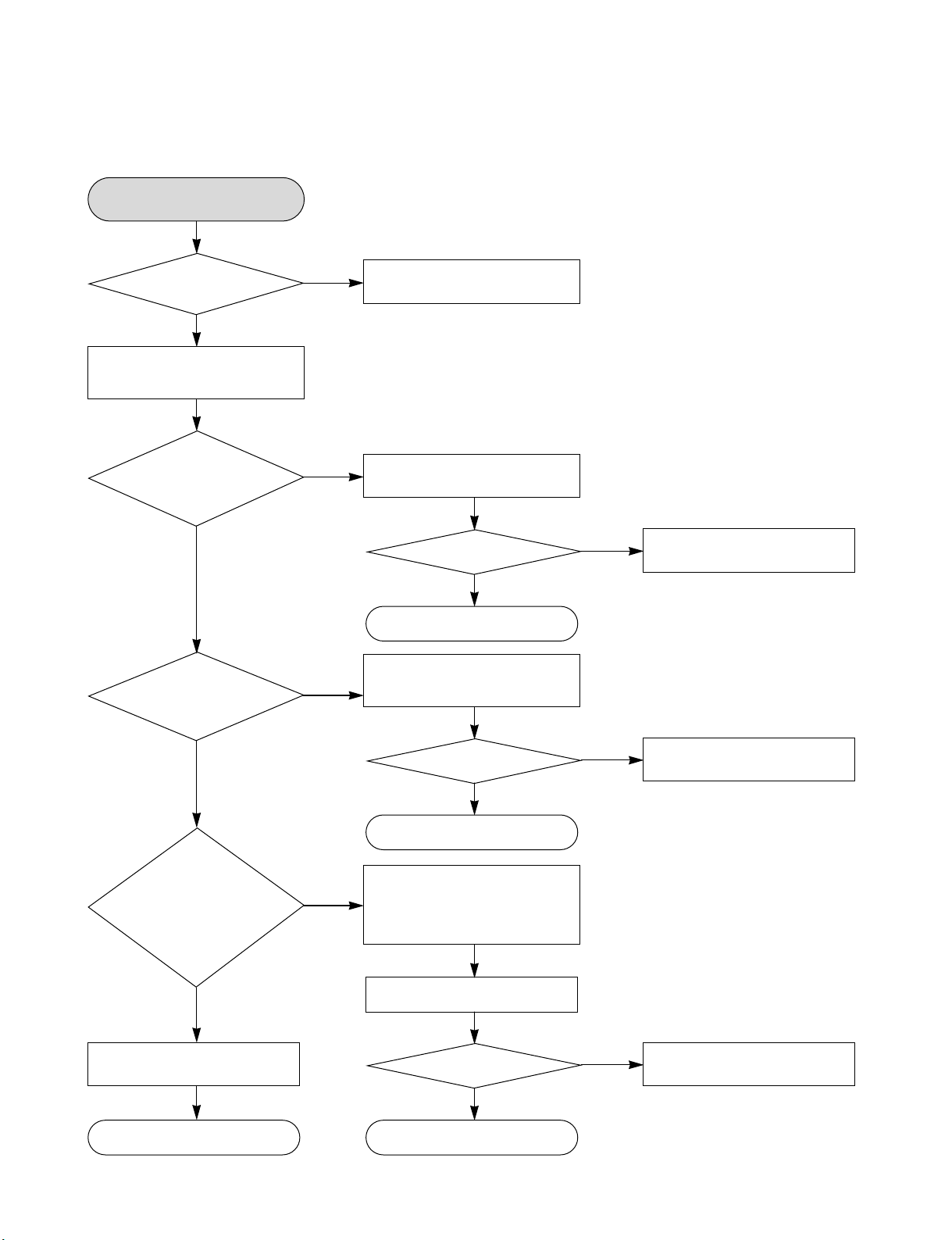
AUDIO ELECTRICAL TROUBLESHOOTING GUIDE
1. POWER (SMPS)
No .5.6VA
YES
Is the F101 normal? Replace the F101 (Use the same fuse)
YES
Is the BD101 normal? Replace the BD101
YES
Is the TH101 normal? Replace the R101
YES
NO
NO
NO
Is Vcc (9V - 18V)
supplied to IC101 Pin2?
YES
IS the D959 normal? Replace the D959
YES
Is there about 2.5V at the
IC103 Pin1?
YES
Is the IC102 normal? Replace the IC102
YES
Is the D947 normal? Replace the D947
YES
Is the D949 normal? Replace the D949
YES
Is the D940 normal? Replace the D940
NO
NO
NO
NO
NO
NO
NO
Is the D102 normal?
NO
Check or Replace the D102
Replace the IC103
YES
Is the D943 normal? Replace the D943
YES
Is the D941 normal? Replace the D941
YES
NO
NO
Power line of main PCB is short
3-1

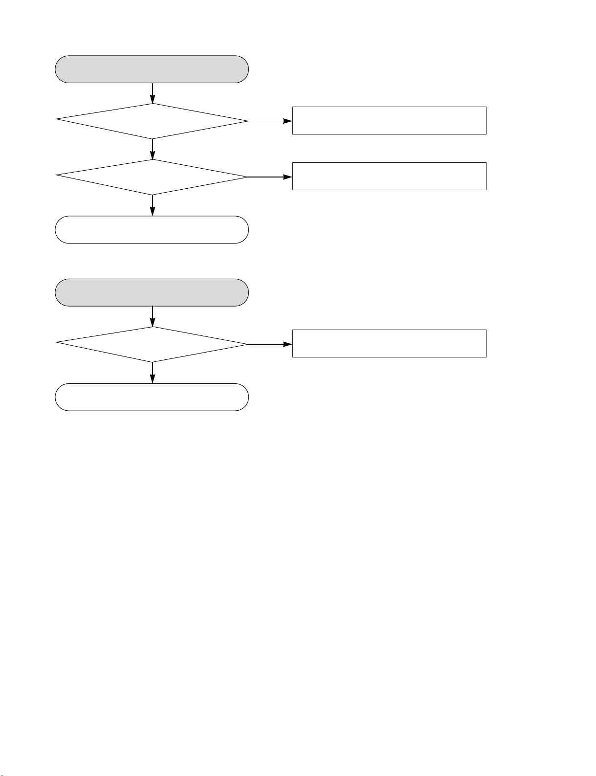
No 5.0V
YES
Is the Vcc(5.6V)
supplied to IC957 pin1?
YES
Is the IC957 pin4 “H”?
YES
Check or Replace the IC957
No 3.3V
YES
Is the Vcc(4.2V)
supplied to IC955 pin1?
YES
Is the IC955 pin4 “H”?
NO
NO
NO
NO
Check or Replace the D959
Check the CD CTL “H”
signal from µ-com
Check or Replace the D943
Check the P CTL “H”
signal from µ-com
YES
Check or Replace the IC955
No 12V
YES
Is the Vcc(13.5V)
supplied to IC947 pin1?
YES
Is the IC947 pin4 “H”?
YES
Check or Replace the IC947
NO
NO
Check or Replace the D940
Check the P CTL “H”
signal from µ-com
3-2
No -12V
YES
Is the voltage 0f
C932 -13V
YES
Is the IC155 pin2
12V?
YES
Check or Replace the Q942
No VF+
YES
Is the ZD950
Normal?
YES
Replace the R993 or Q950, Q943
NO
NO
NO
Check or Replace the D970
Check the PWR CTL
“H” signal from µ-com
Replace the ZD950
3-3
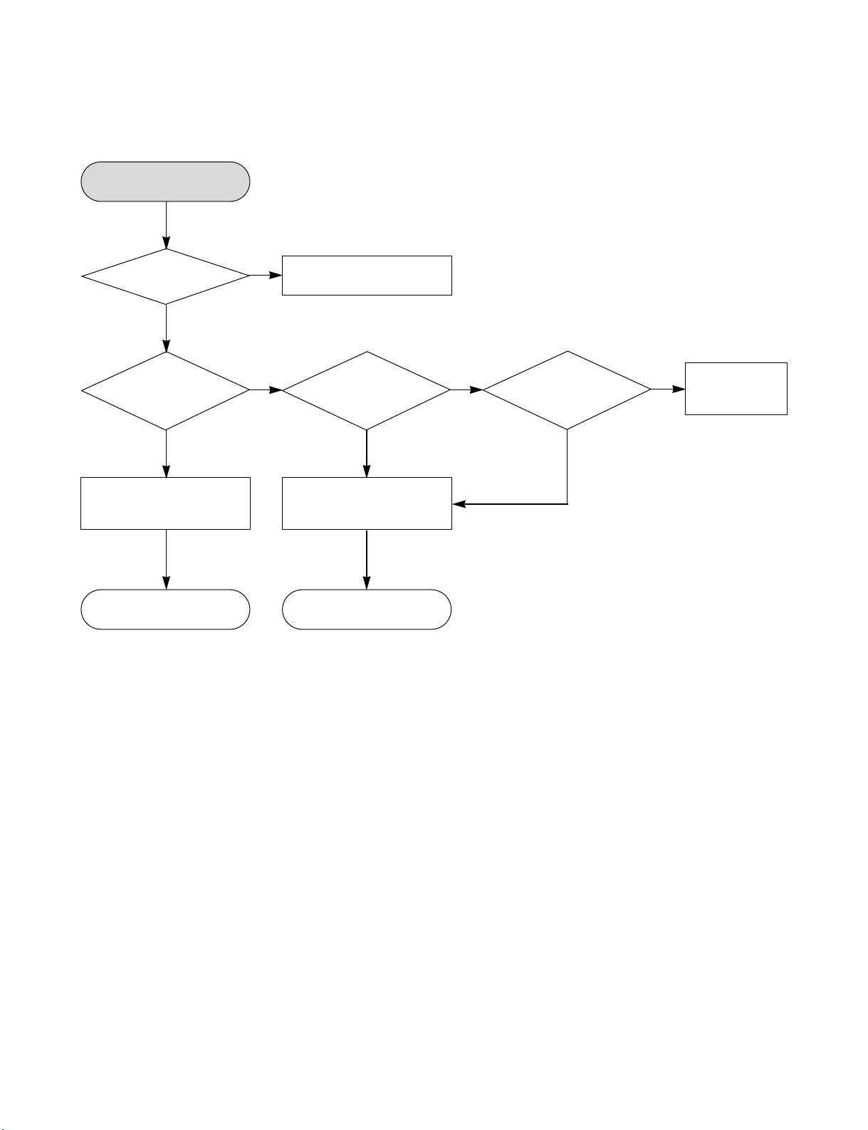
2. MICOM PART CHECK I
MICOM part check I
YES
Check P-SENS
(P7904)_PIN6.
YES
Check both
end voltage of IC101
(KIA7042).
YES
Check voltage of IC100
78KO/KF2_PIN1.
YES
OK OK
NO
SMPS troubleshooting.
NO
Check if IC101(KIA7042) of
output voltage is over 4.3V.
Refer to
Check
if input voltage of
IC101(KIA7042) is
over 5V.
YES
YES
NO
Check the
periphery of IC101
(KIA7042).
YES
NO
Replace IC101
(KIA7042).
3-4

3. MICOM PART CHECK II
MICOM part check II
YES
voltage of P7904_PIN5
Check if
is 5.6V.
YES
Check
both end voltage of
D101
YES
Check
Q101_ emitter/collector
5V.
YES
NO
NO
NO NO
Refer to
SMPS troubleshooting.
Check if output of
D101(RL104) is 5V.
YES
Check D101.
YES
OK
Check Q102_base
0.6V HIGH.
YES
NO
Replace D101.
Check if output of IC101
(KIA7042) is over 4.3V.
YES
Check if IC103_PIN8 and
IC100_PIN19, 20, 59 are 5V.
YES
X101 : 32.768kHz
X100 : 9.8304MHz
Check the operation.
YES
OK
Q102_collector 0.6V LOW.
YES
Check Q102.
YES
OK
3-5
NO
Check IC101.
YES
OK
Replace Q102.
NO
Replace IC101.
4. IC103(KS4CD21CS) CHECK
Check
IC100(78KOKF2)_
PIN 22, 24
YES
PIN22
DATA PIN24 CLK
YES
OK
Check micom
voltage 5V.
YES
Check micom.
YES
OK
NONO
NO
Refer to
micom troubleshooting
Replace micom.
3-6
5. FLD DISPLAY CHECK
FLD display check
YES
P7904_PIN1, 2, 3 voltage
Check
input.
YES
Check if both end votage
of F1, F2 are over 3.7V.
VKK : over 26V.
YES
Check WF31
connection and power.
Pin1 : FL-22 Pin2 : FL+26
Pin3 : VKK- over
26V.
YES
Check
IC301(PT6324) voltage.
Pin50 VKK : -26V
PIN9.52 : +5V
NO
NO
NO
Refer to SMPS
Check WF31 connection.
YES
Check each
PIN voltage.
YES
OK
If voltage is not 5V,
check input and output
of D301(1SR35).
YES
NO
Replace WF31.
YES
IC100 - >
Check IC301
DATA communication.
PIN PIN
75PIN - > 3PIN STB
76PIN - > 2PIN D
78PIN - > 1PIN
CLK
YES
YES
NO
Check IC301.
YES
OK
IC100
75 PIN - > STB
77 PIN - > 4PIN DI
78 PIN - > 1PIN CLK
Check data output.
YES
76 PIN - > DO - - >
Check DATA in Check IC100.
YES
Check IC100.
YES
OKOK
3-7
NO
NO
Replace IC301.
Replace IC100FLD light on?
 Loading...