

LG U960 Service Manual
Date: June, 2007 / Issue 1.0
Service Manual
Model : U960
Service Manual
U960
U960 cover(10.0)_0626 1904.1.7 5:32 PM ˘`1

- 3 -
1. INTRODUCTION .............................. 5
1.1 Purpose................................................... 5
1.2 Regulatory Information............................ 5
2. PERFORMANCE...............................7
2.1 System Overview.....................................7
2.2 Usable environment.................................8
2.3 Radio Performance..................................8
2.4 Current Consumption.............................14
2.5 RSSI BAR ..............................................14
2.6 Battery BAR ...........................................15
2.7 Sound Pressure Level............................16
2.8 Charging ................................................16
3. TECHNICAL BRIEF ........................17
3.1 General Description ...............................17
3.2 GSM Mode.............................................19
3.3 UMTS Mode...........................................23
3.4 LO generation and distribution circuits...25
3.5 Off-chip RF Components .......................25
3.6 Digital Baseband (DBB / MSM6280)......34
3.7 Hardware Architecture ...........................35
3.8. Subsystem of MSM6280.......................37
3.9. External memory interface....................45
3.10. Hardware sub system .........................46
3.11. DVB-H System....................................73
3.12 Main Features......................................80
4. TROUBLE SHOOTING ...................86
4.1 RF Component.......................................86
4.2 SIGNAL PATH_UMTS RF .....................88
4.3 SIGNAL PATH_GSM RF .......................89
4.4 Checking VCTCXO Block ......................90
4.5 Checking Front-End Module Block ........92
4.6 Checking UMTS Block...........................94
4.7 Checking GSM Block.............................99
4.8 Checking Bluetooth Block....................105
4.9 Power on trouble..................................107
4.10 USB trouble........................................109
4.11 SIM detect trouble..............................110
4.12 Key sense trouble ..............................111
4.13 Camera trouble ..................................112
4.14 Main LCD trouble...............................113
4.15 Keypad backlight trouble....................115
4.16 Folder on/off trouble...........................116
4.17 Micro SD trouble ................................117
4.18 Audio trouble......................................118
4.19 Charging trouble ................................128
4.20 DVB-H broadcasting signal reception
trouble ................................................131
5. DOWNLOAD .................................135
5.1 Introduction ..........................................135
5.2 Downloading Procedure.......................135
5.3 Troubleshooting Download Errors .......145
5.4 Caution.................................................149
6. BLOCK DIAGRAM ........................150
6.1 GSM & UMTS RF Block.......................150
6.2 Interface Diagram ................................152
7. Circuit Diagram ............................157
8. PCB LAYOUT................................169
9. Calibration & RF Auto Test
Program (Hot Kimchi)..................177
9.1 Structure of HOT-KIMCHI Program .....177
9.2 Usage of Hot-Kimchi............................179
10. Factory Test Mode .....................182
10.1. Test Program Setting........................182
10.2. WCDMA Test Mode..........................183
10.3. GSM Test Mode................................184
11. EXPLODED VIEW &
REPLACEMENT PART LIST ..... 185
11.1 EXPLODED VIEW ............................ 185
11.2 Replacement Parts
<Mechanic component>.................... 189
<Main component> ........................... 192
11.3 Accessory ......................................... 213
Table Of Contents

- 4 -

- 5 -
1.1 Purpose
This manual provides the information necessary to repair, calibration, description and download the
features of this model.
1.2 Regulatory Information
A. Security
Toll fraud, the unauthorized use of telecommunications system by an unauthorized part (for example,
persons other than your company’s employees, agents, subcontractors, or person working on your
company’s behalf) can result in substantial additional charges for your telecommunications services.
System users are responsible for the security of own system.
There are may be risks of toll fraud associated with your telecommunications system. System users
are responsible for programming and configuring the equipment to prevent unauthorized use. The
manufacturer does not warrant that this product is immune from the above case but will prevent
unauthorized use of commoncarrier telecommunication service of facilities accessed through or
connected to it. The manufacturer will not be responsible for any charges that result from such
unauthorized use.
B. Incidence of Harm
If a telephone company determines that the equipment provided to customer is faulty and possibly
causing harm or interruption in service to the telephone network, it should disconnect telephone
service until repair can be done. A telephone company may temporarily disconnect service as long as
repair is not done.
C. Changes in Service
A local telephone company may make changes in its communications facilities or procedure. If these
changes could reasonably be expected to affect the use of the phones or compatibility with the net
work, the telephone company is required to give advanced written notice to the user, allowing the user
to take appropriate steps to maintain telephone service.
D. Maintenance Limitations
Maintenance limitations on the phones must be performed only by the manufacturer or its authorized
agent. The user may not make any changes and/or repairs expect as specifically noted in this manual.
Therefore, note that unauthorized alternations or repair may affect the regulatory status of the system
and may void any remaining warranty.
1. INTRODUCTION
1. INTRODUCTION
E. Notice of Radiated Emissions
This model complies with rules regarding radiation and radio frequency emission as defined by local
regulatory agencies. In accordance with these agencies, you may be required to provide information
such as the following to the end user.
F. Pictures
The pictures in this manual are for illustrative purposes only; your actual hardware may look slightly
different.
G. Interference and Attenuation
A phone may interfere with sensitive laboratory equipment, medical equipment, etc. Interference from
unsuppressed engines or electric motors may cause problems.
H. Electrostatic Sensitive Devices
ATTENTION
Boards, which contain Electrostatic Sensitive Device (ESD), are indicated by the sign.
Following information is ESD handling:
• Service personnel should ground themselves by using a wrist strap when exchange system boards.
• When repairs are made to a system board, they should spread the floor with anti-static mat which is
also grounded.
• Use a suitable, grounded soldering iron.
• Keep sensitive parts in these protective packages until these are used.
• When returning system boards or parts like EEPROM to the factory, use the protective package as
described.
1. INTRODUCTION
- 6 -

2. PERFORMANCE
- 7 -
2.1 System Overview
2. PERFORMANCE
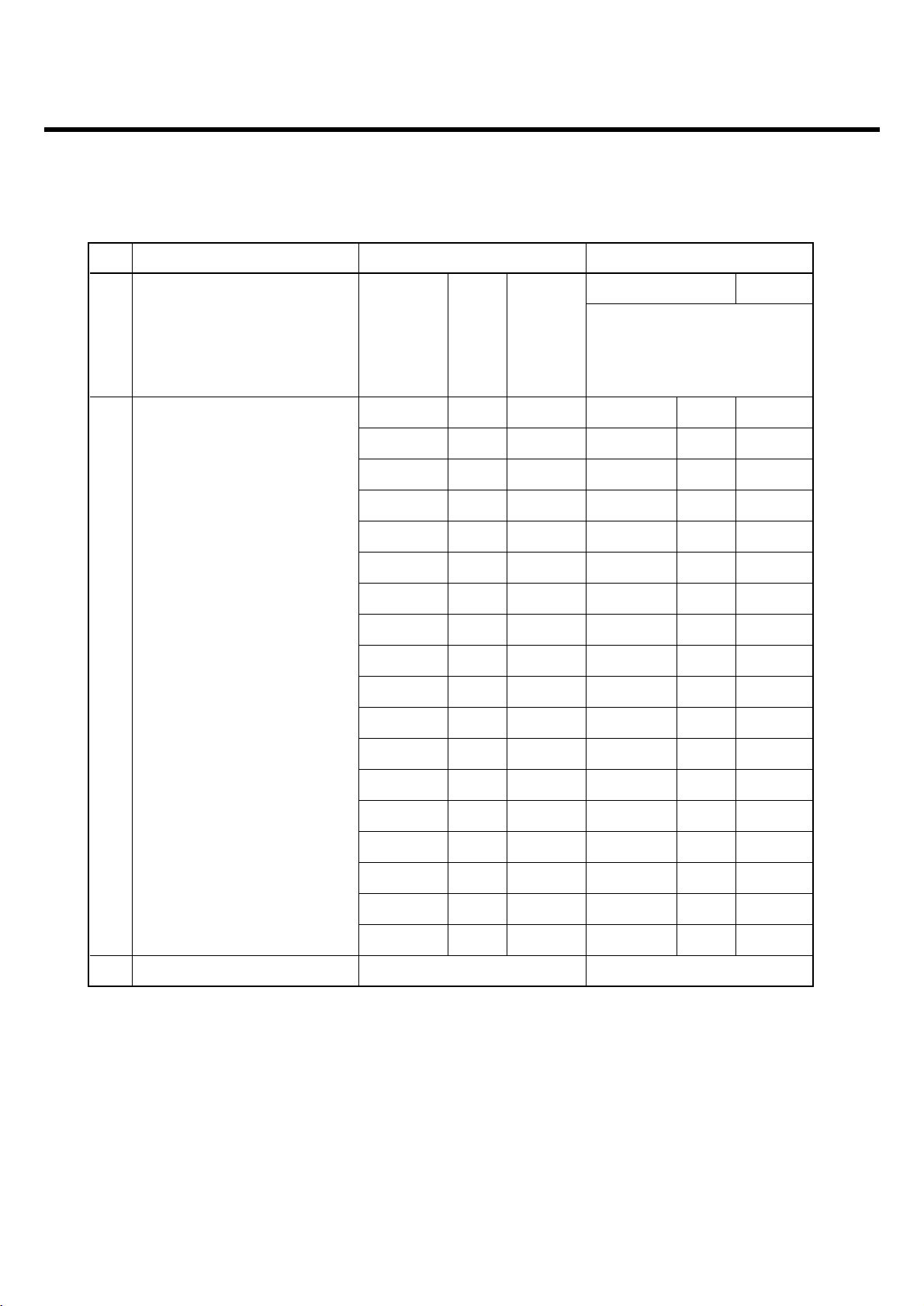
Item Specification
Shape GSM900/1800/1900 and WCDMA Bar Swing Type
Size 104 x 52.6 x 19.3 mm
Weight Under 117g (with 950mAh Battery)
Power 3.7V normal, 950 mAh Li-Polymer
Talk Time Over 170 min (WCDMA, Tx=12 dBm, Voice)
(with 950mAh) Over 178 min (GSM, Tx=Max, Voice)
Standby Time Over 250 Hrs (WCDMA, DRX=1.28)
(with 950mAh) Over 280 Hrs (GSM, Paging period=9)
Antenna Internal and external type Antenna(DVBH)
LCD Main 2.4” 262K 240 X 320 pixel TFT (QVGA LCD Module)
LCD Backlight White LED Back Light (main only)
Camera Dual Camera ; 2 Mega pixel (CMOS), VGA Camera (CMOS)
Vibrator Yes (Cylinder Type)
LED Indicator No
MIC Yes
Receiver Yes
Earphone Jack Yes
Connectivity Bluetooth, USB
Volume Key Push Type(+, -)
External Memory Trans-Flash
I/O Connect 18 Pin
2.2 Usable environment
1) Environment
2) Environment (Accessory)
* CLA : 12 ~ 24 V(DC)
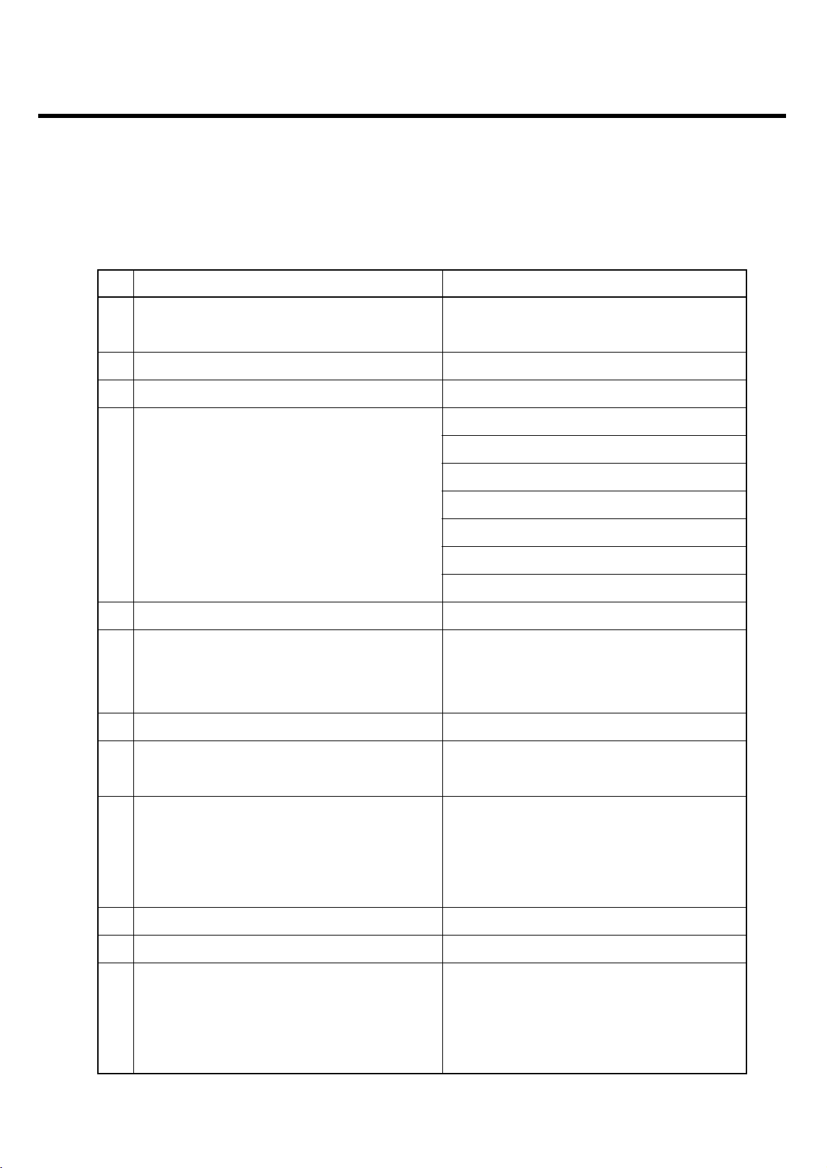
2.3 Radio Performance
1) Transmitter - GSM Mode
* In case of DCS : [A] -> 1710, [B] -> 1785 * In case of PCS : [A] -> 1850, [B] -> 1910
2. PERFORMANCE
- 8 -
Item Specification
Voltage 3.7 V(Typ), [Shut Down : 3.23V]
Operation Temp -20 ~ +60°C
Storage Temp -20 ~ +70°C
Humidity 85 % (Max)
Reference Spec. Min Typ. Max Unit
TA Power Available power 100 220 240 Vac
No Item GSM DCS & PCS
100k~1GHz -39dBm
9k ~ 1GHz -39dBm
MS allocated 1G~[A]MHz -33dBm
Channel
1G~12.75GHz -33dBm
[A]M~[B]MHz -39dBm
Conducted [B]M~12.75GHz -33dBm
1Spurious 100k~880MHz -60dBm 100k~880MHz -60dBm
Emission 880M~915MHz -62dBm 880M~915MHz -62dBm
Idle Mode
915M~1GHz -60dBm 915M~1GHz -60dBm
1G~[A]MHz -50dBm 1G~[A]MHz -50dBm
[A]M~[B]MHz -56dBm [A]M~[B]MHz -56dBm
[B]M~12.5GHz -50dBm [B]M~12.5GHz -50dBm
2. PERFORMANCE
- 9 -
* In case of DCS : [A] -> 1710, [B] -> 1785 * In case of PCS : [A] -> 1850, [B] -> 1910
No Item GSM DCS & PCS
30M ~ 1GHz -36dBm
30M~1GHz -36dBm
MS allocated 1G~[A]MHz -30dBm
Channel
1G ~ 4GHz -30dBm
[A]M~[B]MHz -36dBm
Radiated [B]M~4GHz -30dBm
2Spurious 30M ~ 880MHz -57dBm 30M~880MHz -57dBm
Emission 880M ~ 915MHz -59dBm 880M~915MHz -59dBm
Idle Mode
915M~1GHz -57dBm 915M~1GHz -57dBm
1G~[A]MHz -47dBm 1G~[A]MHz -47dBm
[A]M~[B]MHz -53dBm [A]M~[B]MHz -53dBm
[B]M~4GHz -47dBm [B]M~4GHz -47dBm
3 Frequency Error ±0.1ppm ±0.1ppm
4 Phase Error
±5(RMS) ±5(RMS)
±20(PEAK) ±20(PEAK)
3dB below reference sensitivity 3dB below reference sensitivity
Frequency Error RA250 : ±200Hz RA250: ±250Hz
5 Under Multipath and HT100 : ±100Hz HT100: ±250Hz
Interference Condition TU50 : ±100Hz TU50: ±150Hz
TU3 : ±150Hz TU1.5: ±200Hz
0 ~ 100kHz +0.5dB 0 ~ 100kHz +0.5dB
200kHz -30dB 200kHz -30dB
250kHz -33dB 250kHz -33dB
Due to 400kHz -60dB 400kHz -60dB
Output RF
modulation 600 ~ 1800kHz -66dB 600 ~ 1800kHz -60dB
6 1800 ~ 3000kHz -69dB 1800 ~ 6000kHz -65dB
Spectrum
3000 ~ 6000kHz -71dB ≥6000kHz -73dB
≥6000kHz -77dB
Due to
400kHz -19dB 400kHz -22dB
Switching
600kHz -21dB 600kHz -24dB
transient
1200kHz -21dB 1200kHz -24dB
1800kHz -24dB 1800kHz -27dB
2. PERFORMANCE
- 10 -
No Item GSM DCS & PCS
Frequency offset 800kHz
7 Intermodulation attenuation –
Intermodulation product should
be Less than 55dB below the
level of Wanted signal
Power control
Power Tolerance
Power control
Power Tolerance
Level (dBm) (dB) Level (dBm) (dB)
533±3 030±3
631±3 128±3
729±3 226±3
827±3 324±3
925±3 422±3
10 23 ±3 5 20 ±3
8Transmitter Output Power 11 21 ±3 6 18 ±3
12 19 ±3 7 16 ±3
13 17 ±3 8 14 ±3
14 15 ±3 9 12 ±4
15 13 ±3 10 10 ±4
16 11 ±5 11 8 ±4
17 9 ±5 12 6 ±4
18 7 ±5 13 4 ±4
19 5 ±5 14 2 ±5
15 0 ±5
9 Burst timing Mask IN Mask IN
2. PERFORMANCE
- 11 -
2) Transmitter - WCDMA Mode
No Item Specification
1 Maximum Output Power Class 3 : +24dBm(+1/-3dB)
Class 4 : +21dBm(±2dB)
2Frequency Error ±0.1ppm
3 Open Loop Power control in uplink ±9dB@normal, ±12dB@extreme
Adjust output(TPC command)
cmd 1dB 2dB 3dB
+1 +0.5/1.5 +1/3 +1.5/4.5
4 Inner Loop Power control in uplink 0 -0.5/+0.5 -0.5/+0.5 -0.5/+0.5
-1 -0.5/-1.5 -1/-3 -1.5/-4.5
Group (10 equel command group)
+1 +8/+12 +16/+24
5 Minimum Output Power -50dBm(3.84MHz)
Qin/Qout : PCCH quality levels
6Out-of-synchronization handling of output power Toff@DPCCH/Ior : -22 -> -28dB
Ton@DPCCH/Ior : -24 -> -18dB
7 Transmit OFF Power -56dBm(3.84MHz)
8 Transmit ON/OFF Time Mask
±25us
PRACH,CPCH,uplinlk compressed mode
±25us
9 Change of TFC
Power varies according to the data rate
DTX : DPCH off
(minimize interference between UE)
10 Power setting in uplink compressed ±3dB(after 14slots transmission gap)
11 Occupied Bandwidth(OBW) 5MHz(99%)
-35-15*(∆f-2.5)dBc@∆f=2.5~3.5MHz,30k
12 Spectrum emission Mask
-35-1*(∆f-3.5)dBc@∆f=3.5~7.5MHz,1M
-39-10*(∆f-7.5)dBc@∆f=7.5~8.5MHz,1M
-49dBc@∆f=8.5~12.5MHz,1M
3)Receiver - GSM Mode
2. PERFORMANCE
- 12 -
No Item Specification
13 Adjacent Channel Leakage Ratio(ACLR)
33dB@5MHz, ACP>-50dBm
43dB@10MHz, ACP>-50dBm
-36dBm@f=9~150KHz, 1K BW
-36dBm@f=50KHz~30MHz, 10K BW
-36dBm@f=30MHz~1000MHz, 100K BW
14
Spurious Emissions -30dBm@f=1~12.5GHz, 1M BW
(*: additional requirement) (*)-41dBm@f=1893.5~1919.6MHz, 300K
(*)-67dBm@f=925~935MHz, 100K BW
(*)-79dBm@f=935~960MHz, 100K BW
(*)-71dBm@f=1805~1880MHz, 100K BW
15 Transmit Intermodulation
-31dBc@5MHz,Interferer -40dBc
-41dBc@10MHz, Interferer -40dBc
16 Error Vector Magnitude (EVM)
17.5%(>-20dBm)
(@12.2K, 1DPDCH+1DPCCH)
17 Transmit OFF Power
-15dB@SF=4.768Kbps, Multi-code
transmission
No Item GSM DCS & PCS
1
Sensitivity (TCH/FS Class II) -105dBm -105dBm
2
Co-Channel Rejection
C/Ic=7dB Storage -30 ~ +85
(TCH/FS Class II, RBER, TU high/FH)
3 Adjacent Channel 200kHz C/Ia1=-12dB C/Ia1=-12dB
Rejection 400kHz C/Ia2=-44dB C/Ia2=-44dB
Wanted Signal :-98dBm Wanted Signal :-96dBm
4
Intermodulation Rejection 1st interferer:-44dBm 1st interferer:-44dBm
2nd interferer:-45dBm 2nd interferer:-44dBm
5
Blocking Response Wanted Signal :-101dBm Wanted Signal :-101dBm
(TCH/FS Class II, RBER)
Unwanted : Depend on Frequency Unwanted : Depend on Frequency

2. PERFORMANCE
- 13 -
4) Receiver - WCDMA Mode
No Item Specification
1 Reference Sensitivity Level -106.7 dBm(3.84 MHz)
-25dBm(3.84MHz)
2Maximum Input Level -44dBm/3.84MHz(DPCH_Ec)
UE@+20dBm output power(Class3)
3 Adjacent Channel Selectivity (ACS)
33dB
UE@+20dBm output power(Class3)
-56dBm/3.84MHz@10MHz
4In-band Blocking UE@+20dBm output power(Class3)
-44dBm/3.84MHz@15MHz
UE@+20dBm output power(Class3)
-44dBm/3.84MHz@f=2050~2095 and
2185~2230MHz
UE@+20dBm output power(Class3)
-30dBm/3.84MHz@f=2025~2050 and
5 Out-band Blocking 2230~2255MHz
UE@+20dBm output power(Class3)
-15dBm/3.84MHz@f=1~2025 and
2255~12500MHz
UE@+20dBm output power(Class3)
6Spurious Response
-44dBm CW
UE@+20dBm output power(Class3)
-46dBm CW@10MHz
7Intermodulation Characteristic -46dBm/3.84MHz@20MHz
UE@+20dBm output power(Class3)
-57dBm@f=9KHz~1GHz, 100K BW
8 Spurious Emissions -47dBm@f=1~12.5GHz, 1M BW
-60dBm@f=1920MHz~1980MHz, 3.84M BW
-60dBm@f=2110MHz~2170MHz, 3.84M BW
2. PERFORMANCE
- 14 -
2.4 Current Consumption
1) U960 Current Consumption
(Stand by Test Condition : Bluetooth off, LCD backlight off)
(Call Test Condition : Bluetooth off, LCD backlight dimming mode)
(VT Test Condition : Speaker off, LCD backlight On)
2.5 RSSI BAR
Stand by Voice Call VT
WCDMA
Under 3.8 mA Under 335 mA Under 543mA
(DRX=1.28) (Tx=12dBm) (Tx=12dBm)
Under 3.39 mA Under 319 mA
GSM
(Paging period = 9) (PCL=5)
Level Change WCDMA GSM
BAR 4 → 3 -87 ± 2 dBm -91 ± 2 dBm
BAR 3 → 2 -97 ± 2 dBm -96 ± 2 dBm
BAR 2 → 1-107 ± 2 dBm -101 ± 2 dBm
BAR 1 → 0-112 ± 2 dBm -106 ± 2 dBm
2.6 Battery BAR
2. PERFORMANCE
- 15 -
Indication Standby
Bar 4 Over 3.83 ± 0.05V
Bar 4 → 3 3.82 ± 0.05V
Bar 3 → 2 3.72 ± 0.05V
Bar 2 → 1 3.67 ± 0.05V
Bar 1 → Empty 3.50 ± 0.05V
Low Voltage, 3.50± 0.05V (Stand-by) / 3.50 ± 0.05V (Talk)
Warning message+ Blinking [Interval : 3min(Stand-by) / 1min(Talk)]
Power Off 3.23 ± 0.05V
2. PERFORMANCE
- 16 -
2.7 Sound Pressure Level
2.8 Charging
- Charging Method : CC & CV (Constant Current & Constant Voltage)
- Maximum Charging Voltage : 4.2V
- Maximum Charging Current : 650mA
- Nominal Battery Capacity : 950 mAh
- Charger Voltage : 4.8V
- Charging time : Max 3 h (Except time trickle charging)
- Full charge indication current (icon stop current) : 70mA
- Low battery POP UP : 3.50V
- Low battery alarm interval : Idle - 3 min, Dedicated - 1min
- Cut-off voltage : 3.23V
No Test Item Specification
1 Sending Loudness Rating (SLR) 8 ±3 dB
2 Receiving Loudness Rating (RLR)
Nor -4 ± 3 dB
Max -15 ± 3 dB
3 Side Tone Masking Rating (STMR) Min 17 dB
4 Echo Loss (EL) Min 40 dB
5 Sending Distortion (SD) Refer to Table 30.3
6 Receiving Distortion (RD) Refer to Table 30.4
7 Idle Noise-Sending (INS) Max -64 dBm0p
8 Idle Noise-Receiving (INR)
Nor Under -47 dBPA
Max Under -36 dBPA
9 Sending Loudness Rating (SLR) 8±3dB
10 Receiving Loudness Rating (RLR)
Nor -1 ±3 dB
Max -12 ±3 dB
11 Side Tone Masking Rating (STMR) Min 25 dB
12 Echo Loss (EL) Min 40 dB
13 Sending Distortion (SD) Refer to Table 30.3
14 Receiving Distortion (RD) Refer to Table 30.4
15 Idle Noise-Sending (INS) Max -55 dBm0p
16 Idle Noise-Receiving (INR)
Nor Under -45 dBPA
Max Under -40 dBPA
TDMA Noise
-. GSM : Power Level : 5
DCS/PCS : Power Level : 0
(Cell Power : -90 ~ -105 dBm)
17
-. Acoustic (Max Vol.)
MS/Headset SLR : 8 ±3dB
MS/Headset RLR : -15 ± 3dB/-12dB
(SLR/RLR : Mid-value setting)
MS
Headset
MS and
Headset
Max
Under -62 dBm
3. TECHNICAL BRIEF
- 17 -
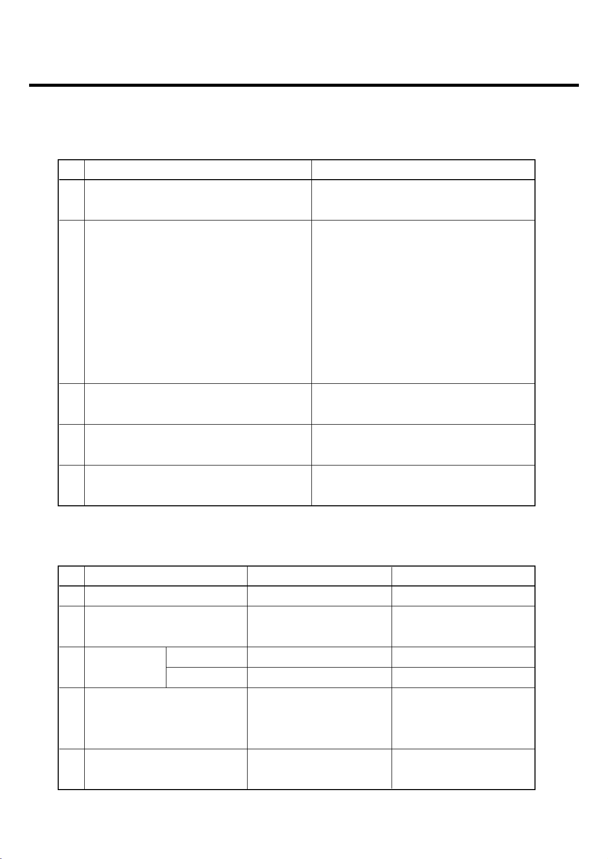
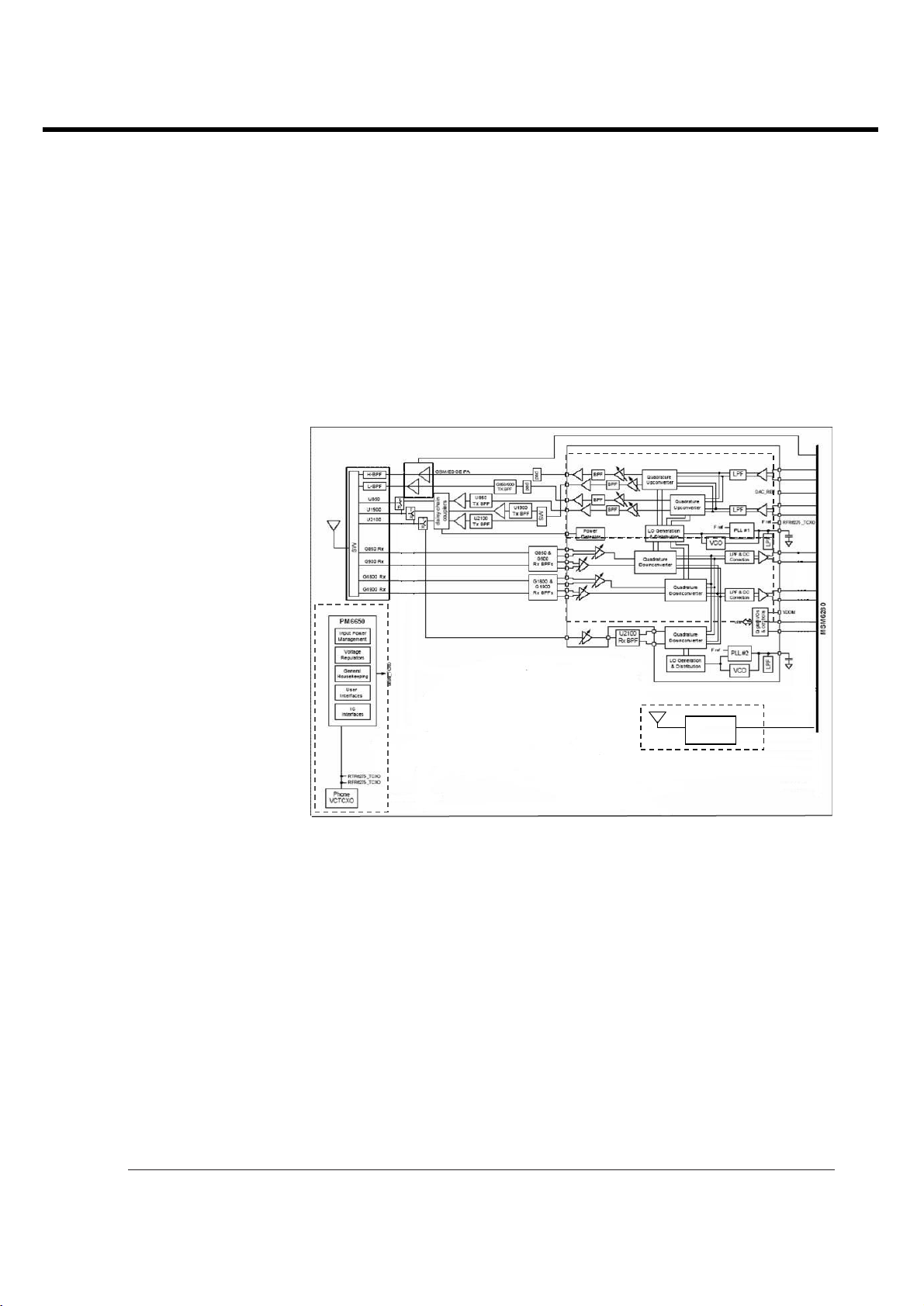
3.1 General Description
The U960 supports UMTS-2100, GSM-900, DCS-1800, and PCS-1900 based GSM/GPRS/UMTS. All
receivers and the UMTS transmitter use the radioOne1Zero-IF architecture to eliminate intermediate
frequencies, directly converting signals between RF and baseband. The quad-band GSM transmitters
use a baseband-to-IF upconversion followed by an offset phase-locked loop that translates the GMSKmodulated or 8-PSKmodulated signal to RF.
1
QUALCOMM’s branded chipset that implements a Zero-IF radio architecture.
3. TECHNICAL BRIEF
UMTS (2100)
GSM ( 9 0 0 , 1800, 1900)
Bluetoot h
1. RTR6275 fo r GSM Tx
and WCDMA Tx
2. RTR6275 fo r GSM/EDGE
Rx and WCDMA Rx
3. Bluetooth RF module
4. PM6650 f or power
management
1
2
4
3
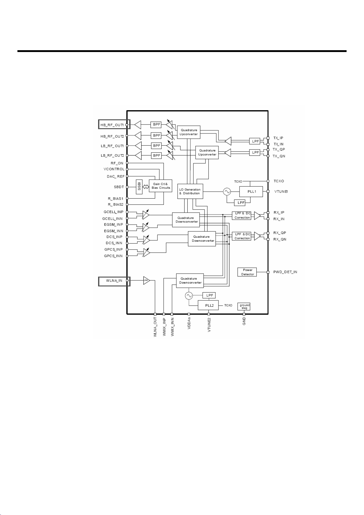
[Fig 1.1] Block diagram of RF part

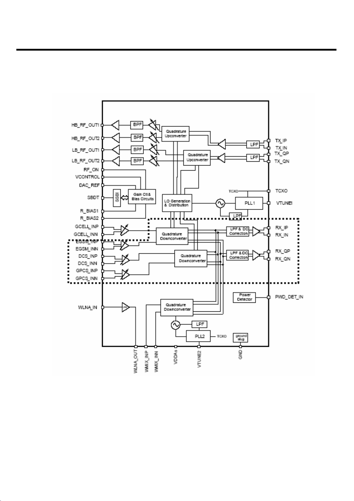
A generic, high-level functional block diagram of U960 is shown in Figure 1-1. One antenna collects
base station forward link signals and radiates handset reverse link signals. The antenna connects with
receive and transmit paths through a FEM(Front End Module).
The UMTS receive paths each include an LNA, an RF band-pass filter, and a downconverter that
translate the signal directly from RF-to-baseband using radioOne ZIF techniques. The RFIC’s Rx
analog baseband outputs, for the receive chains, connect to the MSM IC. The UMTS and GSM Rx
baseband outputs share the same inputs to the MSM IC.
For the transmit chains, the RTR6275 IC directly translates the Tx baseband signals (from the MSM
device) to an RF signal using an internal LO generated by integrated on-chip PLL and VCO. The
RTR6275 IC outputs deliver fairly high-level RF signals that are first filtered by Tx SAWs and then
amplified by their respective UMTS PAs. The high- and low-band UMTS RF transmit signals emerge
from the RTR6275 transceiver.
In the GSM receive path, the received RF signals are applied through their band-pass filters and
down-converted directly to baseband in the RTR6275 transceiver IC. These baseband outputs are
shared with the UMTS receiver and routed to the MSM IC for further signal processing.
The GSM/EDGE transmit path employs one stage of up-conversion and, in order to improve efficiency,
is divided into phase and amplitude components to produce an open-loop Polar topology:
1. The on-chip quadrature up-converter translates the GMSK-modulated signal or 8-PSK modulated
signal, to a constant envelope phase signal at RF;
2. The amplitude-modulated (AM) component is applied to the ramping control pin of Polar power
amplifier from a DAC within the MSM
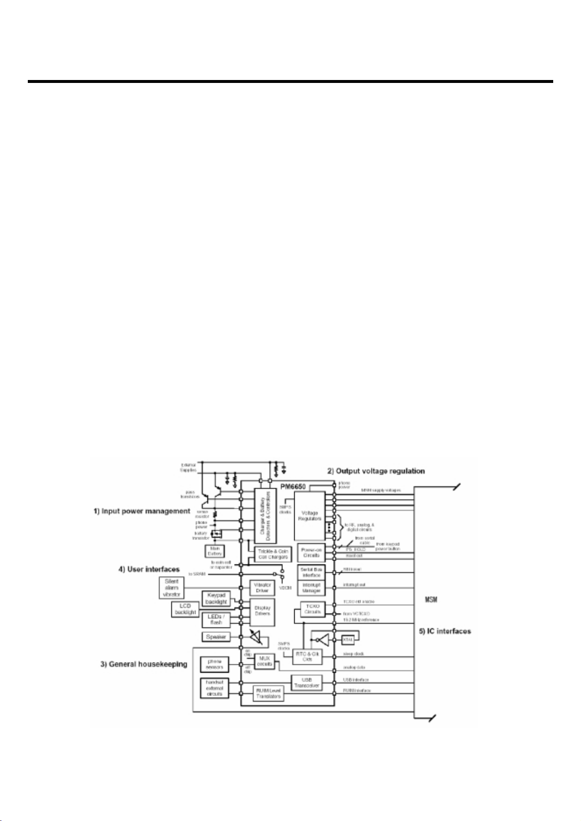
U960 power supply voltages are managed and regulated by the PM6650 Power Management IC. This
versatile device integrates all wireless handset power management, general housekeeping, and user
interface support functions into a single mixed signal IC. It monitors and controls the external power
source and coordinates battery recharging while maintaining the handset supply voltages using low
dropout, programmable regulators.
The device’s general housekeeping functions include an ADC and analog multiplexer circuit for
monitoring on-chip voltage sources, charging status, and current flow, as well as userdefined off-chip
variables such as temperature, RF output power, and battery ID. Various oscillator, clock, and counter
circuits support IC and higher-level handset functions. Key parameters such as under-voltage lockout
and crystal oscillator signal presence are monitored to protect against detrimental conditions.
3. TECHNICAL BRIEF
- 18 -
3. TECHNICAL BRIEF
- 19 -
3.2 GSM Mode
3.2.1 GSM Receiver
The Dual-mode U960’s receiver functions are split between the three RFICs as follows:
• GSM-900, DCS-1800, and PCS-1900 UMTS-2100 modes bot use the RTR6275 IC only. Each mode
has independent front-end circuits and down-converters, but they share common baseband circuits
(with only one mode active at a time). All receiver control functions are beginning with SBI2-controlled
parameters.
RF Front end consists of antenna, antenna switch module(LMSP4LMA-573TEM) which includes four
RX saw filters(GSM850, GSM900, GSM900, DCS and PCS). The antenna switch module allows
multiple operating bands and modes to share the same antenna. In U960, a common antenna
connects to one of six paths: 1) UMTS-2100 Rx/Tx, 2) GSM-900 Rx, 3) GSM-900 Tx, 4) DCS-1800
Rx, and 5) DCS-1800, PCS-1900 Tx(High Band Tx’s share the same path), 6) PCS-1900 Rx. UMTS
operation requires simultaneous reception and transmission, so the UMTS Rx/Tx connection is routed
to a duplexer that separates receive and transmit signals.
GSM900, DCS, and PCS operation is time division duplexed, so only the receiver or transmitter is
active at any time and a frequency duplexer is not required.
2
The RFIC operating modes and circuit parameters are MSM-controlled through the proprietary 3-line Serial Bus Interface (SBI). The Application
Programming Interface (API) is used to implement SBI commands. The API is documented in AMSS Software - please see applicable AMSS
Software documentation for details.
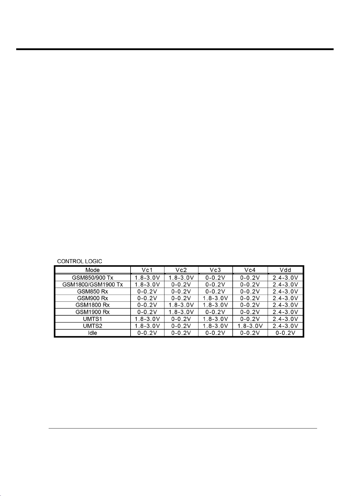
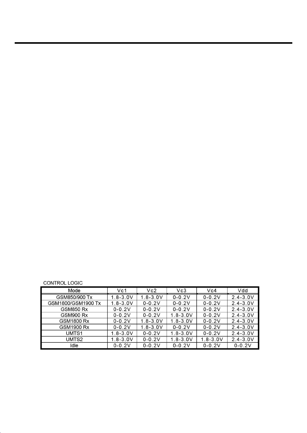
[Table 1.1] Antenna Switch Module Control logic

The GSM900, DCS, and PCS receiver inputs of RTR6275 are connected directly to the transceiver
front-end circuits(filters and antenna switch module). GSM900, DCS, and PCS receiver inputs use
differential configurations to improve common-mode rejection and second-order non-linearity
performance. The balance between the complementary signals is critical and must be maintained from
the RF filter outputs all the way into the IC pins.
Since GSM900, DCS, and PCS signals are time-division duplex (the handset can only receive or
transmit at one time), switches are used to separate Rx and Tx signals in place of frequency duplexers this is accomplished in the switch module.
The GSM900, DCS, and PCS receive signals are routed to the RTR6275 through band selection filters
and matching networks that transform single-ended 50-Ω sources to differential impedances optimized
for gain and noise figure. The RTR input uses a differential configuration to improve second-order intermodulation and common mode rejection performance. The RTR6275 input stages include MSMcontrolled gain adjustments that maximize receiver dynamic range.
The amplifier outputs drive the RF ports of the quadrature RF-to-baseband downconverters.
The downconverted baseband outputs are multiplexed and routed to lowpass filters (one I and one Q)
having passband and stopband characteristics suitable for GMSK or 8-PSK processing. These filter
circuits include DC offset corrections. The filter outputs are buffered and passed on to the MSM6280 IC
for further processing (an interface shared with the RFR6275 UMTS receiver outputs
3. TECHNICAL BRIEF
- 20 -
3. TECHNICAL BRIEF
- 21 -
[Fig 1.2] RTR6275 RX feature
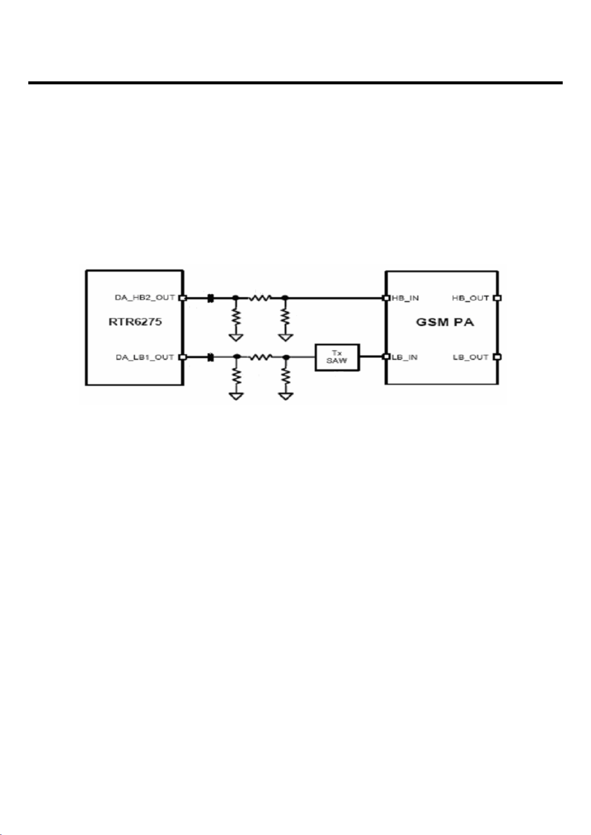
3.2.2 GSM Transmitter
The RTR6275 transmitter outputs(DA_HB2_OUT and DA_LB1_OUT)include on-chip output matching
inductors. 50ohm output impedance is achieved by adding a series capacitor at the output pins. The
capacitor value may be optimized for specific applictions and PCB characteristics based on pass-band
symmetry about the band center frequency, the suggested starting value is shown in Figure1.2.
The RTR6275 IC is able to support GSM 900 and GSM 1800/1900 mode transmitting. This design
guideline shows a tri-band GSM application.
Both high-band and low band outputs are followed by resistive pads to ensure that the load Presented
to the outputs remains close to 50ohm. The low-band GSM. Tx path also includes a Tx-band SAW filter
to remove noise-spurious components and noise that would be amplified by the PA and appear in the
GSM Rx band
3. TECHNICAL BRIEF
- 22 -
91Ω91Ω
6pF
120Ω120Ω
68Ω
5pF
51Ω
[Fig 1.3] GSM Transmitter matching

3. TECHNICAL BRIEF
- 23 -
3.3 UMTS Mode
3.3.1 Receiver
The UMTS duplexer receiver output is routed to LNA circuits within the RTR6275 device.
The UMTS Rx input is provided with an on-chip LNA that amplifies the signal before a second stage
filter that provides differential downconverter. This second stage input is configured differentially to
optimize second-order intermodulation and common mode rejection performance. The gain of the
UMTS frontend amplifier and the UMTS second stage differential amplifier are adjustable, under MSM
control, to extend the dynamic range of the receivers. The second stage UMTS Rx amplifiers drive the
RF ports of the quadrature RF-tobaseband downconverters. The downconverted UMTS Rx baseband
outputs are routed to lowpass filters having passband and stopband characteristics suitable for UMTS
Rx processing. These filter circuits allow DC offset corrections, and their differential outputs are
buffered to interface shared with GSM Rx to the MSM IC. The UMTS baseband outputs are turned off
when the RTR6275 is downconverting GSM signals and on when the UMTS is operating.
3.3.2 Transmitter
The UMTS Tx path begins with differential baseband signals (I and Q) from the MSM device. These
analog input signals are amplified, filtered, and applied to the quadrature up-converter mixers. The upconverter output is amplified by multiple variable gain stages that provide transmit AGC control. The
AGC output is filtered and applied to the driver amplifier; this output stage includes an integrated
matching inductor that simplifies the external matching network to a single series capacitor to achieve
the desired 50-Ω interface.
The RTR6275 UMTS output is routed to its power amplifier through a bandpass filter, and delivers fairly
high-level signals that are filtered and applied to the PA. Transmit power is delivered from the duplexer
to the antenna through the switch module.
The transceiver LO synthesizer is contained within the RTR6275 IC with the exception of the off-chip
loop filter components and the VC-TCXO. This provides a simplified design for multimode applications.
The PLL circuits include a reference divider, phase detector, charge pump, feedback divider, and digital
logic generator.
UMTS Tx. Using only PLL1, the LO generation and distribution circuits create the necessary LO signals
for nine different frequency converters. The UMTS transmitter also employs the ZIF architecture to
translate the signal directly from baseband to RF. This requires FLO to equal FRF, and the RTR6275 IC
design achieves this without allowing FVCO to equal FRF.
The RTR6275 IC is able to support UMTS 2100/1900 and UMTS 850 mode transmitting. This design
guideline shows only UMTS 2100 applications.
3. TECHNICAL BRIEF
- 24 -
[Figure 1.4] RTR6275 IC functional block diagram
WCDMA_2100_TX
WCDMA_2100_RX
3.4 LO generation and distribution circuits
The integrated LO generation and distribution circuits are driven by internal VCOs to support various
modes to yield highly flexible quadrature LO outputs that drive all GSM/EDGE and UMTS band
upconverters and downconverters; with the help of these LO generation and distribution circuits, true
zero-IF architecture is employed in all GSM and UMTS band receivers and transmitters to translate the
signal directly from RF to baseband and from baseband to RF.
Two fully functional fractional-N synthesizers, including VCOs and loop filters, are integrated within the
RTR6275 IC. The first synthesizer (PLL1) creates the transceiver LOs that support the UMTS
2100/1900/1800 transmitter, and all four GSM band receivers and transmitters including: GSM 850,
GSM 900, GSM 1800, and GSM 1900. The second synthesizer (PLL2) provides the LO for the UMTS
2100/1900/1800 receiver. An external TCXO input signal is required to provide the synthesizer
frequency reference to which the PLL is phase and frequency locked. The RTR6275 IC integrates
most of PLL loop filter components on-chip except two off-chip loop filter series capacitors, and
significantly reduces off-chip component requirement. With the integrated fractional-N PLL
synthesizers, the RTR6275 has the advantages of more flexible loop bandwidth control, fast lock time,
and low-integrated phase error
3.5 Off-chip RF Components
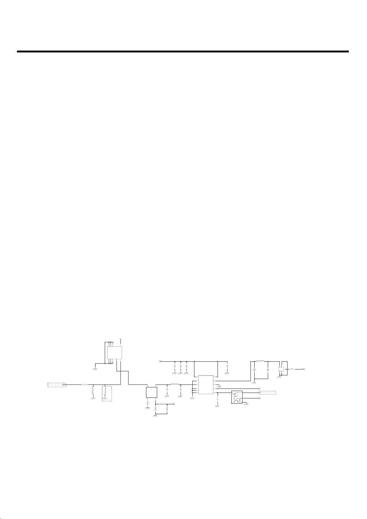
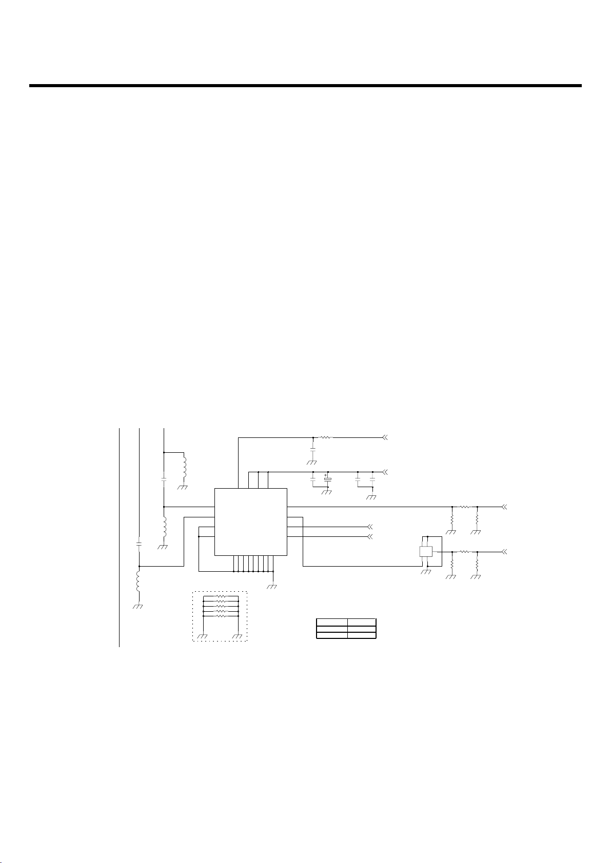
3.5.1 WCDMA PAM (U105: WS2512-TR1G)
The UMTS PA output power is monitored by l power detector circuits(U101 : RTR6275).
This detector voltage can be used for transmitter calibration and monitor to meet RF system
specification.
3. TECHNICAL BRIEF
- 25 -
[Figure 1.5] WCDMA PAM, Duplexer, Coupler
8 dB
20dB
NA
L123
33p
C162
100p
C169
100p
C160
FL103
C163
NA
Q101
2
45
31
KRX102E
R123
51
C164 2.7p
VCC2
10
VCONT
4
5
VREF
WS2512_TR1G
BGND
11
3
GND1
6
GND2
GND3
7
GND49RFIN
2
8
RFOUT
1
VCC1
U105
1nH
C166
C159
0.01u
NA
L124
120
R125
120
R126
C168
0.5p
SCDY0003402
U104
4
50OHM
COUP
3
IN
2
OUT
1
EFCH1950TDF1
FL105
G12G2
3
G3
5
IN
1
O1
4
R124
51
C161
0.01u
10u
C158
1.2p
C167
4
GND2
GND3
89
GND46GND53GND65RX7TX
FL104
SAYZY1G95EA0B00
2
ANT
1
GND1
C165
1.5nH
C157
3.9nH
WCDMA_2100_TX_OUT
RX_WCDMA_2100
PA_R1
+VPWR
PWR_DET
PA_ON
VREG_TCXO_2.85V
3.5.2 VCTCXO (X101 : TG-5010LH(19.2M))
The Voltage Controlled Temperature Compensated Crystal Oscillator (VCTCXO) provides the
reference frequency for all RFIC synthesizers as well as clock generation functions within the
MSM6280 IC. The oscillator frequency is controlled by the MSM6280 IC.s TRK_LO_ADJ pulse density
modulated signal in the same manner as the transmit gain control TX_AGC_ADJ. A two-pole RC
lowpass filter is recommended on this control line.
The PM6650 IC controls the handset power-up sequence, including a special VCTCXO warm-up
interval before other circuits are turned on. This warm-up interval (as well as other TCXO controller
functions) is enabled by the MSM TCXO_EN line . The PM6650 IC VREG_TCXO regulated output
voltage is used to power the VCTCXO and is enabled before most other regulated outputs.
Any GSM mode power control circuits within the MSM6280 IC require a reference voltage for proper
operation and sufficient accuracy. Connecting the PM6650 IC REF_OUT directly to the MSM6275 IC
GSM_PA_PWR_CTL_REF provides this reference. This sensitive analog signal needs a 0.1 •ÏF low
frequency filter near to MSM side, and isolate from digital logic and clock traces with ground on both
sides, plus ground above and below if routed on internal layers.
3.5.3 Front-End Module (FL101 : LMSP4LMA-573TEMP)
This equipment uses a single antenna to support all handset operating modes, with an antenna switch
module select the operating frequency and band. UMTS operation requires simultaneous reception
and transmission, so the UMTS Rx/Tx connection is routed to a duplexer that separates receive and
transmit signals. The active connection is MSM-selected by three control lines (GPIO[9], GPIO[10],
and GPIO[11]). These GPIOs are programmed to be ANT_SEL0_N, ANT_SEL1_N, and
ANT_SEL2_N) respectively.
3. TECHNICAL BRIEF
- 26 -
[Table 1.2] Front End Module control logic

3. TECHNICAL BRIEF
- 27 -
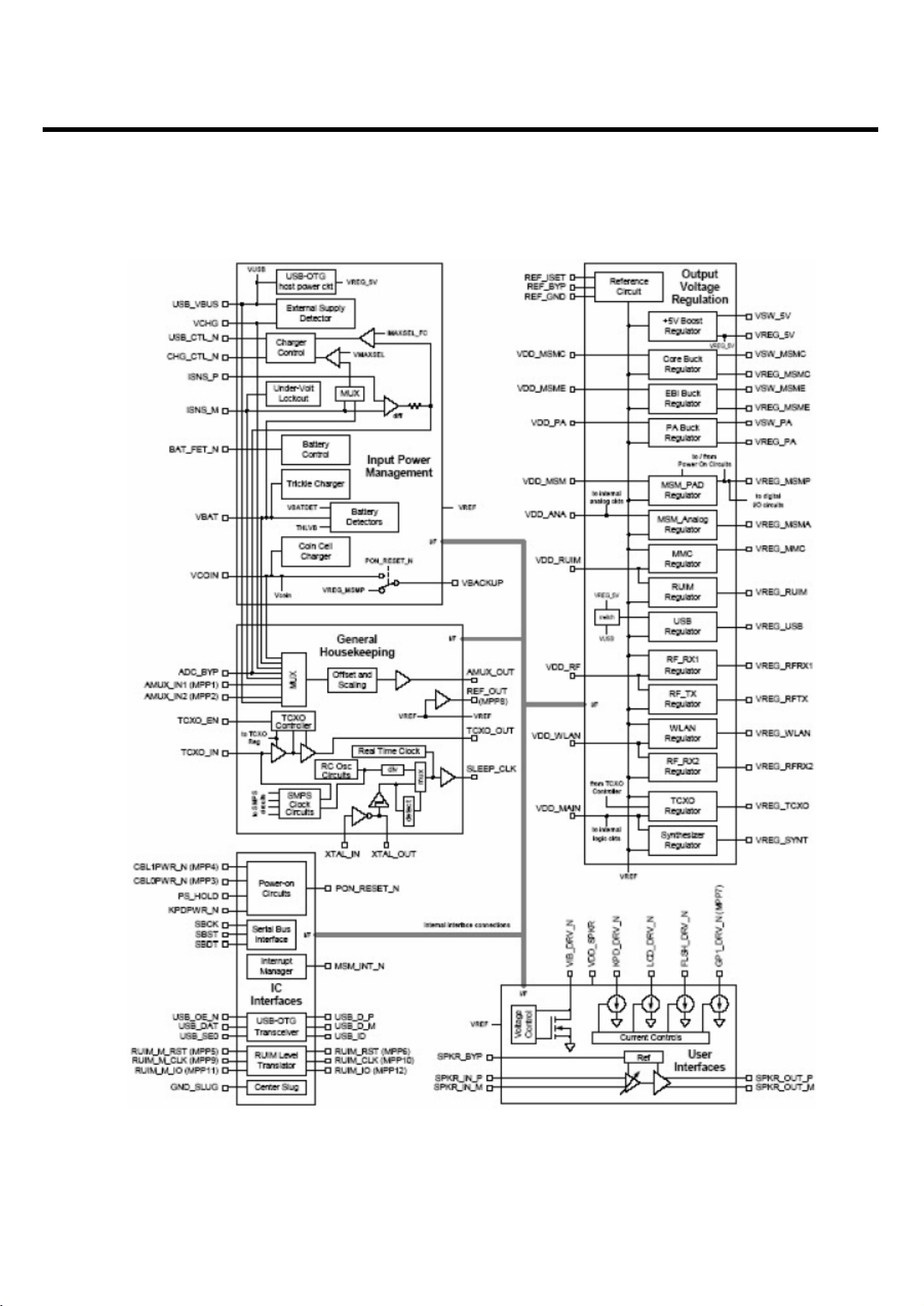
3.5.4 PMIC Functional Block Diagram (U601 : PM6650-2M)
• Input power management
- Valid external supply attachment and removal detection
- Supports unregulated (closed-loop) external charger supplies and USB supplies as input power
sources
- Supports lithium-ion main batteries
- Trickle, constant current, constant voltage, and pulsed charging of the main battery
- Supports coin cell backup battery (including charging)
- Battery voltage detectors with programmable thresholds
- VDD collapse protection
- Charger current regulation and real-time monitoring for over-current protection
- Charger transistor protection by power limit control
- Control drivers for two external pass transistors and one external battery MOSFET-MOSFET is
optional
- Voltage, current, and power control loops
- Automated recovery from sudden momentary power loss
• Output voltage regulation
- One boost (step-up) switched-mode power supply (SMPS) for driving white LEDs and hosting
USBOTG
- Three buck (step-down) switched-mode power supplies that efficiently generate MSMC, MSME,
and PA (or second MSMC) supply voltages
- Supports dynamic voltage scaling (DVS) for MSMC and PA
- Eleven low dropout regulator circuits with programmable output voltages, implemented using three
different current ratings: 300 mA (two), 150 mA (six), and 50 mA (three). These can be used to
power MSMA, MSMP, RFRX1, RFRX2, RFTX, SYNT, TCXO, WLAN, MMC, USB, and RUIM
circuits.
- All regulators can be individually enabled/disabled for power savings
- Low power mode available on MSMA and MSMP regulators
- All regulated outputs are derived from a common bandgap reference-close tracking
• Integrated handset-level housekeeping functions reduces external parts count, size, cost
- Analog multiplexer selects from 8 internal and up to 18 external inputs
- Multiplexer output’s offset and gain are adjusted, increasing the effective ADC resolution
- Adjusted multiplexer output is buffered and routed to an MSM device ADC
- Dual oscillators - 32.768 kHz off-chip crystal and on-chip RC assures MSM device sleep clock
- Crystal oscillator detector and automated switch-over upon lost oscillation
- Real time clock for tracking time and generating associated alarms
- On-chip adjustments minimize crystal oscillator frequency errors
- Circuits control TCXO warm-up and synchronize, deglitch, and buffer the TCXO signal
- TCXO buffer control for optimal QPH/catnap timing
- Three-stage over-temperature protection (smart thermal control)
• Integrated handset-level user interfaces
- Four programmable current sinks recommended as keypad backlight, LCD backlight, camera flash,
and general-purpose drivers
- Vibration motor driver programmable from 1.2 to 3.1V in 100 mV increments
- Speaker driver with programmable gain, turn-on time, and muting; differential operation
(drives external 8 Ω speakers with volume controlled 500 mW)
• IC-level interfaces
- MSM device-compatible 3-line SBI for efficient initialization, status, and control
- Supports the MSM device’s interrupt processing with an internal interrupt manager
- Many functions monitored and reported through real-time and interrupt status signals
- Dedicated circuits for controlled power-on sequencing, including the MSM device’s reset signal
- Several events continuously monitored for triggering power-on/power-off sequences
- Supports and orchestrates soft resets
- USB-OTG transceiver for full-speed (12 Mb/s) and low speed (1.5 Mb/s) interfacing of the MSM
device to computers as a USB peripheral, or connecting the MSM device to other peripherals
- RUIM level translators enable MSM device interfacing with external modules
• Twelve multi-purpose pins that can be configured as digital or analog I/Os, bi-directional I/Os, or
current sinks. Default functions support the RUIM level translators, power-on circuits, analog
multiplexer inputs, an LED driver, and a reference voltage buffer.
• Highly integrated functionality in a small package - 84-pin BCCS with a large center slug for electrical
ground, mechanical stability, and thermal relief
3. TECHNICAL BRIEF
- 28 -
[Figure 1.6] MSM6280 Interface
3. TECHNICAL BRIEF
- 29 -
[Figure1.7] PM6650 Block Diagram
3.5.5. GSM PAM (U102:SKY77318)
The SKY77318 Power Amplifier Module (PAM) is designed in a low profile (1.2 mm), compact form
factor for quad-band cellular handsets comprising GSM850/900, DCS1800, and PCS1900 operation.
The PAM also supports Class 12 General Packet Radio Service (GPRS) multi-slot operation.
The module consists of separate GSM PA and DCS1800/PCS1900 PA blocks, impedancematching
circuitry for 50 Ω input and output impedances and a Power Amplifier Control (PAC) block with an
internal current-sense resistor. The custom BiCMOS integrated circuit provides the internal PAC
function and interface circuitry. Fabricated onto a single Gallium Arsenide (GaAs) die, one
Heterojunction Bipolar Transistor (HBT) PA block supports the GSM bands and the other supports the
DCS1800 and PCS1900 bands. Both PA blocksshare common power supply pins to distribute current.
The GaAs die, the Silicon (Si) die, and the passive components are mounted on a multi-layer laminate
substrate. The assembly is encapsulated with plastic overmold. RF input and output ports of the
SKY77318 are internally matched to a 50 Ω load to reduce the number of external components for a
quadband design. Extremely low leakage current (2.5 µA typical) of the dual PA module maximizes
handset standby time. The SKY77318 also contains bandselect switching circuitry to select GSM (logic
0) or DCS/PCS (logic 1) as determined from the Band Select (BS) signal.
3. TECHNICAL BRIEF
- 30 -
[Figure 1. 8] GSM PAM Schematic
DCS/PCS
MODE
HIGH
8 dB
10 dB
LOW
GSM_PA_BAND
GSM
0.01u
C137
NA
L118
C131
68p
R111
91
R113
51
L115
NA
56p
C135
R110
68
0.01u
C138
120
R114
R120 0
0R119
R118 0
0R117
R116 0
0.01u
C136
C132
33u
C143
56p
R108 2.2K
91
R112
NA
C144
FL102
EFCH897MTDB1
G12G2
3
G3
5
IN
1
O1
4
GND9
21
P_GND
RSVD_GND
19
20
VAPC
VBATT
17
VCC1A
2
VCC1B
6
1
BS
3
DCS_PCS_INDCS_PCS_OUT
15
EGSM_IN
4
EGSM_OUT
11
18
ENABLE
5
GND17GND2
GND3
8
9
GND4
GND5
10
12
GND6
GND7
13
14
GND8
16
U102
SKY77318
R115
120
+VPWR
GSM_PA_BAND
DCS_PCS_TX
GSM_TX
GSM_PA_RAMP
GSM_PA_EN

3. TECHNICAL BRIEF
- 31 -
3.5.6 UMTS Duplexer(FL104:SAYZY1G95EA0B00)
A UMTS duplexer splits a single operating band into receive and transmit paths. Important
performance requirements include;
• Insertion loss . this component is also in the receive and transmit paths ; In the U960 typical losses :
UMTS2100_ Tx = 1.28 dB, UMTS2100_ Rx = 1.46 dB
• Out-of-band rejection or attenuation . the duplexer provides input selectivity for the receiver, output
filtering for the transmitter, and isolation between the two. Rejection levels for both paths are
specified over a number of frequency ranges. Two Tx-to-Rx isolation levels are critical to receiver
performance:
• Rx-band isolation . the transmitter is specified for out-of-band noise falling into the Rx band. This
noise leaks from the transmit path into the receive path, and must be limited to avoid degrading
receiver sensitivity. The required Rx-band isolation depends on the PA out of-band noise levels and
Rx-band losses between the PA and LNA. Minimum duplexer Rx band isolation value is about 46.7
dB.
• Tx-band isolation . the transmit channel power also leaks into the receiver. In this case, the leakage
is outside the receiver passband but at a relatively high level. It combines with Rx band jammers to
create cross-modulation products that fall in-band to desensitize the receiver. The required Tx-band
isolation depends on the PA channel power and Txband losses between the PA and LNA. Minimum
duplexer Tx-band isolation value is about 51.7dB.
• Passband ripple . the loss of this fairly narrowband device is not flat across its passband. Passband
ripple increases the receive or transmit insertion loss at specific frequencies, creating performance
variations across the band.s channels, and should be controlled.
• Return loss . minimize mismatch losses with typical return losses of 10 dB or more (VSWR <2:1).
• Power handling . high power levels in the transmit path must be accommodated without degraded
performance. The specified level depends on the operating band class and mobile station class (per
the applicable standard), as well as circuit losses and antenna EIRP. Several duplexer characteristics
depend upon its source and load impedances.
QUALCOMM strongly recommends an isolator be used between the UMTS PA and duplexer to
assure proper performance.
 Loading...