

Page 1

Technical Specification
(TM13LNCAHK1)
1/10
Page 2
History
Written
by
Checked
by
Approved
by
1.0
2018.06.12
Ver. Date Contents
Note
2/10
Page 3

Contents
1. Product Introduction..................................................................................................... 4
1.1 Block Diagram .................................................................................................... 5
1.2 Environmental Specifications .............................................................................. 5
1.3 Electrical Specifications ...................................................................................... 5
1.3.1 Absolute Maximum and ESD Ratings ........................................................... 5
1.3.2 Current Consumption ................................................................................... 6
1.4 Mechanical Specifications ................................................................................. 6
1.4.1 Physical Dimensions and Connection Interface ........................................... 6
1.4.2 Mechanical Drawing ..................................................................................... 7
2. Pin Definitions.............................................................................................................. 8
3 RF Specification ........................................................................................................... 9
3.1. LTE B2,B4, B5,B7,B12,B17 Specification .......................................................... 9
3.2. WCDMA B2, B5 Specification..…………………………………………………… 10
3/10
Page 4
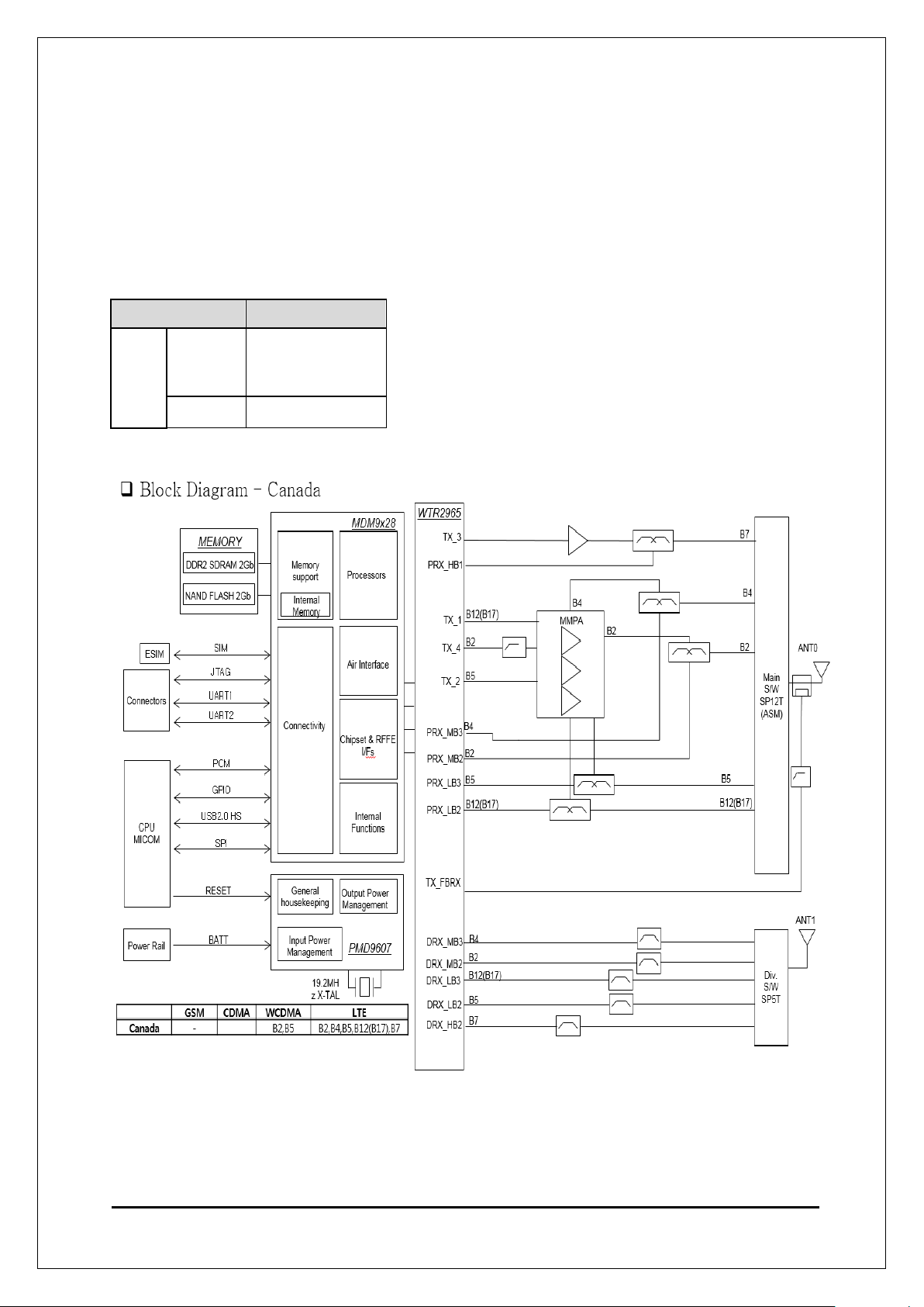
1. Product Introuction
The TM13LNCAHK1 are designed for the automotiv e industry. They sup port LTE and CDMA
air Interface standards. The TM13LNCAHK1 are based on t he Qualco mm M DM 9628 wireless
chipsets and support the followi ng bands.
Table 1. Supported Band
Region US
LTE
Band
WCDMA B2/B5
1.1 Block Diagram
B2/B4/B5/B7/B12
/B17
Figure 1.1. TM13LNCAHK1 Block diagram
4/10
Page 5

1.2 Environmental Specifications
Parameter
Min
Max
Units
+4.0_VPWR
Power Supply Input
-
4.4V
V
VIN
Voltage on any digital input or output pin
-
VREG_MDME+0.5
V
ESD Ratings
ESD1)
Primary, Diversity antenna pads Contact
10
kV
The environmental specification for o peratin g and storage of the TM13LNCAHK1 are de fined
in the the table below.
Table 2. Environmental Specifications
Parameter Temperature Range
Operating Temperature -40℃ to 85℃
Storage Temperature
Humidity 95% or less
-40℃ to +90℃
1.3 Electrical Specifications
This section provides details for some of the key electrical specifications of the
TM13LNCAHK1 embedded modules.
1.3.1 Absolute Maximum Rating and ESD Ratings
This section defines the Absolute Maximum and Electrostatic Discharge (ESD) Ratings of
the TM13LNCAHK1 embedded modules.
Warning: If these parameters are exceeded, even momentarily, damage may occur to the
device.
Table 3. Absolute Maximum Ratings
1) The ESD Simulator configured with 330pF, 2000Ω.
Caution: The TM13LNCAHK1 embedded modules are sensitive to Electrostatic Discharge.
ESD countermeasures and handling methods must be used when handling the
TM13LNCAHK1 devices.
5/10
Page 6
1.3.2 Current Consumption
Mode
Parameter
Typical
Max
Units
Band2/4/7/12/17, Max TX Output /Full RB
600
650
Band5, Max TX Output /Full RB
550
600
Band5
550
600
Band2
600
650
LTE
Idle, Registered
1.8
2.2
mA
WCDMA
Idle, Registered
1.8
2.2
mA
LTE
Sleep Mode, Average Current
1.8
2.2
mA
WCDMA
Sleep Mode, Average Current
1.8
2.2
mA
Parameter
Nominal
Max
Units
Overall Dimension
34 x 40
34.35 x 40.35
mm
Overall Module Height
3.5
3.85
mm
PCB Thickness
1.0
1.1
mm
Flatness Specification
0.1
mm
Weight
12
TBD
g
Table 4. TM13LNCAHK1 Current Consu mption (TBD)
LTE
WCDMA
mA
mA
1.4 Mechanical Specifications
1.4.1 Physical Dimensions and C onnection Interface
The TM13LNCAHK1 embedded modules are a Land Grid Array (LGA) form factor device.
The device does not have a System or RF connectors. All electrical and mechanical
connections are made via the 323 pad TM13LNCAHK1 on the underside of the PCB.
Table5. TM13LNNAHK1 Embedded Module Dimensions
6/10
Page 7

1.4.2 Mechanical Drawing
HMC_MDM9628
module_Pinmap.xls
40 mm
34
1.4.2.1 Module PCB
2. Pin Definitions
2.1 PIN Definitions
7/10
Page 8

Technology
Standards
LTE
• 3GPP Release 8
WCDMA
• 3GPP Release 9
Measure Max and Min and Min Transmit Power
of Low Channel (18650)
Max Power : 20.3~25.7dBm
Min Power : ≤ -39dBm
Measure Max and Min Transmit Power of Mid
Channel (18900)
Max Power : 20.3~25.7dBm
Min Power : ≤ -39dBm
Measure Max and Min Transmit Power of High
Channel (19150)
Max Power : 20.3~25.7dBm
Min Power : ≤ -39dBm
Measure Max and Min and Min Transmit Power
of Low Channel (20000)
Max Power : 20.3~25.7dBm
Min Power : ≤ -39dBm
Measure Max and Min Transmit Power of Mid
Channel (20175)
Max Power : 20.3~25.7dBm
Min Power : ≤ -39dBm
Measure Max and Min Transmit Power of High
Channel (20350)
Max Power : 20.3~25.7dBm
Min Power : ≤ -39dBm
Measure Max and Min and Min Transmit Power
of Low Channel (20450)
Max Power : 20.3~25.7dBm
Min Power : ≤ -39dBm
Measure Max and Min Transmit Power of Mid
Channel (20525)
Max Power : 20.3~25.7dBm
Min Power : ≤ -39dBm
Measure Max and Min Transmit Power of High
Channel (20600)
Max Power : 20.3~25.7dBm
Min Power : ≤ -39dBm
Measure Max and Min and Min Transmit Power
of Low Channel (20800)
Max Power : 20.3~25.7dBm
Min Power : ≤ -39dBm
Measure Max and Min Transmit Power of Mid
Channel (21100)
Max Power : 20.3~25.7dBm
Min Power : ≤ -39dBm
Measure Max and Min Transmit Power of High
Channel (21400)
Max Power : 20.3~25.7dBm
Min Power : ≤ -39dBm
Measure Max and Min and Min Transmit Power
of Low Channel (23060)
Max Power : 20.3~25.7dBm
Min Power : ≤ -39dBm
Measure Max and Min Transmit Power of Mid
Channel (23095)
Max Power : 20.3~25.7dBm
Min Power : ≤ -39dBm
Measure Max and Min Transmit Power of High
Channel (23130)
Max Power : 20.3~25.7dBm
Min Power : ≤ -39dBm
3. RF Specification
The specifications for the LTE and CDMA interfaces are defined.
TM13LNCAHK1 is designed to be compliant w ith the s tandard show n in th e table below .
Table20. Standards Compliance
3.1 LTE B2,B4,B5,B7,B12,B17 Specification
3.1.1 LTE TX Output Power
The Maximum / Minimum Transmitter Output Power of the TM13LNCAHK1 are speci fied in
the following table.
Table21. Conducted TX (Transmit) Max output Power Tolerances – LTE Bands
BAND Method (UL CH) Specification
BAND2
UE Ma xi mum
Output Power
BAND4
UE Maximum
Output Power
BAND5
UE Ma xi mum
Output Power
BAND7
UE Ma xi mum
Output Power
BAND12
UE Ma xi mum
Output Power
8/10
Page 9
BAND17
Measure Max and Min and Min Transmit Power
of Low Channel (23780)
Max Power : 20.3~25.7dBm
Min Power : ≤ -39dBm
Measure Max and Min Transmit Power of Mid
Channel (23790)
Max Power : 20.3~25.7dBm
Min Power : ≤ -39dBm
Measure Max and Min Transmit Power of High
Channel (23800)
Max Power : 20.3~25.7dBm
Min Power : ≤ -39dBm
sensitivity : ≤-95
BLER : ≤ 5%
sensitivity : ≤-95
BLER : ≤ 5%
sensitivity : ≤-95
BLER : ≤ 5%
sensitivity : ≤-97
BLER : ≤ 5%
sensitivity : ≤-97
BLER : ≤ 5%
sensitivity : ≤-97
BLER : ≤ 5%
sensitivity : ≤-95
BLER : ≤ 5%
sensitivity : ≤-95
BLER : ≤ 5%
sensitivity : ≤-95
BLER : ≤ 5%
sensitivity : ≤-95
BLER : ≤ 5%
sensitivity : ≤-95
BLER : ≤ 5%
sensitivity : ≤-95
BLER : ≤ 5%
sensitivity : ≤-94
BLER : ≤ 5%
sensitivity : ≤-94
BLER : ≤ 5%
sensitivity : ≤-94
BLER : ≤ 5%
sensitivity : ≤-94
BLER : ≤ 5%
sensitivity : ≤-94
BLER : ≤ 5%
sensitivity : ≤-94
BLER : ≤ 5%
UE Ma xi mum
Output Power
3.1.2 LTE RX Sensitivity
The Receiver Sensitivity of the TM13LNCAHK1 are specified in the following table.
Table22. Conducted RX (Receive) Sensitivity – LTE Bands
BAND Method (DL CH) Specification
BAND2
Reference
sensitivity
level(DUAL)
BAND4
Reference
sensitivity
level(DUAL)
BAND5
Reference
sensitivity
level(DUAL)
BAND7
Reference
sensitivity
level(DUAL)
BAND12
Reference
sensitivity
level(DUAL)
Measure BLER of Low Channel (650)
Measure BLER of Mid Channel (900)
Measure BLER of High Channel (1150)
Measure BLER of Low Channel (2000)
Measure BLER of Mid Channel (2175)
Measure BLER of High Channel (2350)
Measure BLER of Low Channel (2450)
Measure BLER of Mid Channel (2525)
Measure BLER of High Channel (2600)
Measure BLER of Low Channel (2800)
Measure BLER of Mid Channel (3100)
Measure BLER of High Channel (3400)
Measure BLER of Low Channel (5060)
Measure BLER of Mid Channel (5095)
Measure BLER of High Channel (5130)
BAND17
Reference
sensitivity
level(DUAL)
Measure BLER of Low Channel (5780)
Measure BLER of Mid Channel (5790)
Measure BLER of High Channel (5800)
3.2 WCDMA B2/B5 Specification
3.2.1 WCDMA TX Output Power
The Maximum Transmitter Output Pow er o f the TM13LNCAHK1
following table.
9/10
are specified in the
Page 10

Measure Max Transmit Power of Low Channel
(CH= 9263)
Max Power : 20.3~25.7dBm
Measure Max Transmit Power of Middle Channel
(CH= 9400)
Max Power : 20.3~25.7dBm
Measure Max Transmit Power of High Channel
(CH= 9537)
Max Power : 20.3~25.7dBm
Measure Max Transmit Power of Low Channel
(CH=4133)
Max Power : 20.3~25.7dBm
(CH=4175)
Max Power : 20.3~25.7dBm
Measure Max Transmit Power of High Channel
(CH=4232)
Max Power : 20.3~25.7dBm
0.1% @≤-106dBm
0.1% @≤-106dBm
0.1% @≤-106dBm
0.1% @≤-106dBm
0.1% @≤-106dBm
0.1% @≤-106dBm
Table23. Conducted TX ( Transmit) Max output Power Tolerances – WCDMA Bands
Item Method (DL CH) Specification
WCDMA B2
Power Level
WCDMA B5
Power Level
Measure Max Transmit Power of Middle Channel
3.2.2 W
CDMA RX Sensitivity
The Receiver Sensitivity of the TM13LNCAHK1 are specified in the following table.
Table24. Conducted RX (Receive) Sensitivity –WCDMA Bands
Item Method (DL CH) Specification
9663)
WCDMA B2
Power Level
WCDMA B5
Power Level
Measure BER of Low Channel (CH=
Measure BER of Low Channel (CH= 9800)
Measure BER of Low Channel (CH= 9937)
Measure BER of Low Channel (CH=4358)
Measure BER of Low Channel (CH=4400)
Measure BER of Low Channel (CH=4457)
10/10
Page 11

FCC Warning Statement
FCC Part 15.19
This device complies with part 15 of the FCC Rules. Operation is subject to the following two conditions: (1) this device may
not cause harmful interference, and (2) this device must accept any interference received, including interference that may
cause undesired operation.
FCC Part 15.21
Any changes or modifications (including the antennas) to this device that are not expressly approved by the manufacturer may
void the user’s authority to operate the equipment.
Please notice that if the FCC identification number is not visible when the module is installed inside another device,
then the outside of the device into which the module is installed must also display a label referring to the enclosed
module. This exterior label can use wording such as the following: “Contains FCC ID : BEJTM13LNCAHK1” any similar
wording that expresses the same meaning may be used.
Manual Information to the End User
The module is limited to OEM installation ONLY.
The OEM integrator is responsible for ensuring that the end-user has no manual instruction to remove or install module.
The module is limited to installation in mobile application;
A separate approval is required for all other operating configurations, including portable configurations with respect to
Part 2.1093 and difference antenna configurations.
There is requirement that the grantee provide guidance to the host manufacturer for compliance with Part 15B
requirements.
Industry Canada Statement
This device complies with Industry Canada licence-exempt RSS standard(s).
Operation is subject to the following two conditions:
(1) this device may not cause interference, and (2) this device must accept any
interference, including interference that may cause undesired operation of the device.
Le présent appareil est conforme aux CNR d'Industrie Canada applicables aux appareils radio exempts de licence.
L'exploitation est autorisée aux deux conditions suivantes :
(1) l'appareil ne doit pas produire de brouillage, et (2) l'utilisateur de l'appareil doit accepter tout brouillage
radioélectrique subi, mêmesi le brouillage est susceptible d'en compromettre le fonctionnement.
Please notice that if the IC identification number is not visible when the module is installed inside another device,
then the outside of the device into which the module is installed must also display a label referring to the enclosed
module. This exterior label can use wording such as the following: “Contains IC: 2703H-TM13LNCAHK1 any
similar wording that expresses the same meaning may be used.
L’étiquette d’homologation d’un module d’Innovation, Sciences et Développement économique Canada devra être
posée sur le produit hôte à un endroit bien en vue, en tout temps. En l’absence d’étiquette, le produit hôte doit
porter une étiquette sur laquelle figure le numéro d’homologation du module d’Innovation, Sciences et
Développement économique Canada, précédé du mot « contient », ou d’une formulation similaire allant dans le
même sens et qui va comme suit :
Contient IC : 2703H-TM13LNCAHK1 est le numéro d’homologation du module
Manual Information to the End User
The OEM integrator has to be aware not to provide information to the end user regarding how to install or remove
this RF module in the user’s manual of the end product which integrates this module.
The end user manual shall include all required regulatory information/warning as shown in this manual.
FCC and IC RF Radiation Exposure Statement: This equipment complies with FCC and IC RF Radiation
exposure limits set forth for an uncontrolled environment. This device and its antenna must not be co-located or
operating in conjunction with any other antenna or transmitter.
This equipment should be installed and operated with a minimum distance of 20 cm between the radiator and
your body.
RF du FCC et IC d'exposition aux radiations: Cet équipement est conforme à l'exposition de FCC et IC
rayonnements RF limites é-tablies pour un environnement non contrôlé. L’antenne pour ce transmetteur ne doit
pas être même endroit avec d’autres émetteur sauf conformément à FCC et IC procédures de produits Multiémetteur.
Cet équipement doit être installé et utilisé avec une distance minimale de 20 cm entre le radiateur et votre corps.
 Loading...