

Page 1

MODEL: SR906SB (SR906SB, SH96SB-S/ F/ C, SH95TA-W)SERVICE MANUAL
Internal Use Only
Website http://biz.lgservice.com
5.1ch SURROUND COMPACT
RECEIVER SYSTEM
SERVICE MANUAL
MODEL: SR906SB
CAUTION
BEFORE SERVICING THE UNIT, READ THE “SAFETY PRECAUTIONS”
IN THIS MANUAL.
JUNE, 2011AFN33798528 : ON/P
(SR906SB, SH96SB-S/ F/ C, SH95TA-W)
Page 2

CONTENTS
SECTION 1 ........ SUMMARY
SECTION 2 ........ ELECTRICAL
SECTION 3 ........ CABINET & MAIN CHASSIS
SECTION 4 ........ REPLACEMENT PARTS LIST
1-1
Page 3

SECTION 1
SUMMARY
CONTENTS
PRODUCT SAFETY SERVICING GUIDELINES FOR AV RECEIVER SYSTEM PRODUCTS................ 1-3
SERVICING PRECAUTIONS .......................................................................................................................... 1-4
• GENERAL SERVICING PRECAUTIONS
• INSULATION CHECKING PRODEDURE
• ELECTROSTATICALLY SENSITIVE (ES) DEVICES
SERVICE INFORMATION FOR EEPROM (MICOM) .................................................................................... 1-5
VERIFICATION PROGRAM VERSION AND MICOM OPTION ................................................................... 1-6
FIRMWARE UPDATE ...................................................................................................................................... 1-7
SPECIFICATIONS ............................................................................................................................................ 1-8
1-2
Page 4

PRODUCT SAFETY SERVICING GUIDELINES
FOR AV RECEIVER SYSTEM PRODUCTS
IMPORTANT SAFETY NOTICE
This manual was prepared for use only by properly trained audio-video service
technicians.
When servicing this product, under no circumstances should the original design be
modified or altered without permission from LG Corporation. All components should
be replaced only with types identical to those in the original circuit and their physical
location, wiring and lead dress must conform to original layout upon completion of
repairs.
Special components are also used to prevent x-radiation, shock and fire hazard.
These components are indicated by the letter “x” included in their component designators and are required to maintain safe performance. No deviations are allowed
without prior approval by LG Corporation.
Circuit diagrams may occasionally differ from the actual circuit used. This way,
implementation of the latest safety and performance improvement changes into the
set is not delayed until the new service literature is printed.
CAUTION : Do not attempt to modify this product in any way. Never perform cus-
tomized installations without manufacturer’s approval. Unauthorized modifications
will not only void the warranty, but may lead to property damage or user injury.
Service work should be performed only after you are thoroughly familiar with these
safety checks and servicing guidelines.
GRAPHIC SYMBOLS
The exclamation point within an equilateral triangle is intended to
alert the service personnel to important safety information in the
service literature.
The lightning flash with arrowhead symbol within an equilateral
triangle is intended to alert the service personnel to the presence of
noninsulated “dangerous voltage” that may be of sufficient magnitude
to constitute a risk of electric shock.
The pictorial representation of a fuse and its rating within an equilateral triangle is intended to convey to the service personnel the
following fuse replacement caution notice:
CAUTION : FOR CONTINUED PROTECTION AGAINST RISK
OF FIRE, REPLACE ALL FUSES WITH THE SAME TYPE AND
RATING AS MARKED NEAR EACH FUSE.
SERVICE INFORMATION
While servicing, use an isolation transformer for protection from AC line shock. After
the original service problem has been corrected, make a check of the following:
FIRE AND SHOCK HAZARD
1. Be sure that all components are positioned to avoid a possibility of adjacent
component shorts. This is especially important on items trans-ported to and from
the repair shop.
2. Verify that all protective devices such as insulators, barriers, covers, shields,
strain reliefs, power supply cords, and other hardware have been reinstalled per
the original design. Be sure that the safety purpose of the polarized line plug has
not been defeated.
3. Soldering must be inspected to discover possible cold solder joints, solder
splashes, or sharp solder points. Be certain to remove all loose foreign particles.
4. Check for physical evidence of damage or deterioration to parts and components, for frayed leads or damaged insulation (including the AC cord), and
replace if necessary.
5. No lead or component should touch a high current device or a resistor rated at 1
watt or more. Lead tension around protruding metal surfaces must be avoided.
6. After reassembly of the set, always perform an AC leakage test on all exposed
metallic parts of the cabinet (the channel selector knobs, antenna terminals,
handle and screws) to be sure that set is safe to operate without danger of
electrical shock. DO NOT USE A LINE ISOLATION TRANSFORMER DURING
THIS TEST. Use an AC voltmeter having 5000 ohms per volt or more sensitivity
in the following manner: Connect a 1500 ohm, 10 watt resistor, paralleled by a
.15 mfd 150V AC type capacitor between a known good earth ground water pipe,
conduit, etc.) and the exposed metallic parts, one at a time. Measure the AC voltage across the combination of 1500 ohm resistor and .15 mfd capacitor. Reverse
the AC plug by using a non-polarized adaptor and repeat AC voltage measurements for each exposed metallic part. Voltage measured must not exceed 0.75
volts RMS. This corresponds to 0.5 milliamp AC. Any value exceeding this limit
constitutes a potential shock hazard and must be corrected immediately.
TIPS ON PROPER INSTALLATION
1. Never install any receiver in a closed-in recess, cubbyhole, or closely fitting shelf
space over, or close to, a heat duct, or in the path of heated air flow.
2. Avoid conditions of high humidity such as: outdoor patio installations where dew
is a factor, near steam radiators where steam leakage is a factor, etc.
3. Avoid placement where draperies may obstruct venting. The customer should
also avoid the use of decorative scarves or other coverings that might obstruct
ventilation.
4. Wall- and shelf-mounted installations using a commercial mounting kit must
follow the factory-approved mounting instructions. A product mounted to a shelf
or platform must retain its original feet (or the equivalent thickness in spacers) to
provide adequate air flow across the bottom. Bolts or screws used for fasteners
must not touch any parts or wiring. Perform leakage tests on customized installations.
5. Caution customers against mounting a product on a sloping shelf or in a tilted
position, unless the receiver is properly secured.
6. A product on a roll-about cart should be stable in its mounting to the cart.
Caution the customer on the hazards of trying to roll a cart with small casters
across thresholds or deep pile carpets.
7. Caution customers against using extension cords. Explain that a forest of extensions, sprouting from a single outlet, can lead to disastrous consequences to
home and family.
1-3
Page 5

SERVICING PRECAUTIONS
CAUTION: Before servicing the AV RECEIVER SYSTEM covered by this service data and its supplements and addends,
read and follow the SAFETY PRECAUTIONS.
NOTE: if unforeseen circumstances create conflict between
the following servicing precautions and any of the safety
precautions in this publications, always follow the safety precautions.
Remember Safety First :
General Servicing Precautions
1. Always unplug the AV RECEIVER SYSTEM AC power cord
from the AC power source before:
(1) Removing or reinstalling any component, circuit board,
module, or any other assembly.
(2) Disconnecting or reconnecting any internal electrical
plug or other electrical connection.
(3) Connecting a test substitute in parallel with an electro-
lytic capacitor.
Caution : A wrong part substitution or incorrect polar-
ity installation of electrolytic capacitors may result in an
explosion hazard.
2. Do not spray chemicals on or near this AV RECEIVER
SYSTEM or any of its assemblies.
Electrostatically Sensitive (ES) Devices
Some semiconductor (solid state) devices can be damaged
easily by static electricity. Such components commonly are
called Electrostatically Sensitive (ES) Devices. Examples of
typical ES devices are integrated circuits and some field effect
transistors and semiconductor chip components.
The following techniques should be used to help reduce the
incidence of component damage caused by static electricity.
1. Immediately before handling any semiconductor component or semiconductor-equipped assembly, drain off any
electrostatic charge on your body by touching a known
earth ground. Alternatively, obtain and wear a commercially
available discharging wrist strap device, which should be
removed for potential shock reasons prior to applying power
to the unit under test.
2. After removing an electrical assembly equipped with ES
devices, place the assembly on a conductive surface such
as aluminum foil, to prevent electrostatic charge buildup or
exposure of the assembly.
3. Use only a grounded-tip soldering iron to solder or unsolder
ES devices.
3. Unless specified otherwise in this service data, clean electrical contacts by applying an appropriate contact cleaning
solution to the contacts with a pipe cleaner, cotton-tipped
swab, or comparable soft applicator.
Unless specified otherwise in this service data, lubrication of
contacts is not required.
4. Do not defeat any plug/socket B+ voltage interlocks with
whitch instruments covered by this service manual might be
equipped.
5. Do not apply AC power to this AV RECEIVER SYSTEM
and / or any of its electrical assemblies unless all solidstate
device heat sinks are correctly installed.
6. Always connect the test instrument ground lead to an
appropriate ground before connecting the test instrument
positive lead. Always remove the test instrument ground
lead last.
Insulation Checking Procedure
Disconnect the attachment plug from the AC outlet and turn
the power on. Connect an insulation resistance meter (500V)
to the blades of the attachment plug. The insulation resistance
between each blade of the attachment plug and accessible
conductive parts (Note 1) should be more than 1Mohm.
Note 1 : Accessible Conductive Parts include Metal panels,
Input terminals, Earphone jacks,etc.
4. Use only an anti-static solder removal device. Some solder
removal devices not classified as “anti-static” can generate
electrical charges sufficient to damage ES devices.
5. Do not use freon-propelled chemicals. These can generate
an electrical charge sufficient to damage ES devices.
6. Do not remove a replacement ES device from its protective
package until immediately before you are ready to install
it. (Most replacement ES devices are packaged with leads
electrically shorted together by conductive foam, aluminum
foil,or comparable conductive material).
7. Immediately before removing the protective material from
the leads of a replacement ES device, touch the protective
material to the chassis or circuit assembly into which the
device will be installed.
Caution: Be sure no power is applied to the chassis or cir-
cuit, and observe all other safety precautions.
8. Minimize bodily motions when handling unpackaged
replacement ES devices. (Normally harmless motion such
as the brushing together of your clothes fabric or the lifting
of your foot from a carpeted floor can generate static electricity sufficient to damage an ES device.)
1-4
Page 6
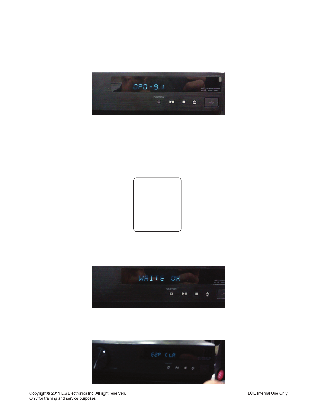
SERVICE INFORMATION FOR EEPROM (MICOM)
1. ENTER THE MICOM OPTION CHANGING MODE
1)
At any function, press front ‘STOP’ button and remote control ‘2’ key for 5 seconds. Enter the MICOM option setting menu.
2. ADJUST MICOM OPTION USING REMOTE CONTROL DIRECTION KEY
1) Using up / down direction key (preset +, -), change option value.
2) Using left / right direction key (tunning +, -), select next option.
DETECT NEW EEPROM
(OPTION EDIT SCREEN)
NAME HEX
OP0
OP1
OP2
OP3
OP4
OP5
09
BE
20
C6
00
C0
3. COMPLETE OPTION CHANGING.
1) After entering option code, press ‘ENTER’ key. You can confi rm ‘WRITE OK’.
2) Next, press front ‘STOP’ button and remote control ‘2’ key. ‘E2P CLR’ display on VFD.
Finish option code changing.
1-5
Page 7
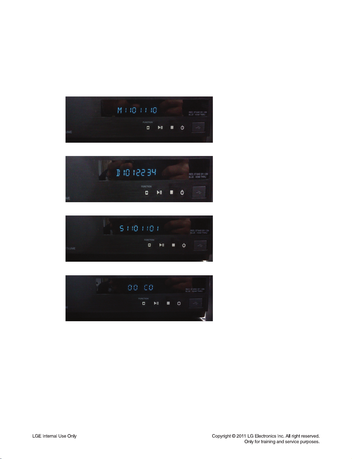
VERIFICATION PROGRAM VERSION AND MICOM OPTION
1. ENTER THE VERIFICATION MODE
1) At any function, press front ‘STOP’ button and remote control ‘PLAY’ key for 5 seconds.
Enter the Program Version and MICOM Option code verifi cation mode.
2) Using left/right key, you can confi rm program version and MICOM option.
MICOM Version
DSP Version
2. RETURN TO FUNCTION
1) After checking, press remote control ‘PLAY’ key for 5 seconds.
Return to function that before you’re set.
MCS Version
MICOM option
1-6
Page 8
FIRMWARE UPDATE
1. COPY AN UPDATE FILE TO USB (USB OR CD-ROM)
Update File Name: MICOM_SR906_1XXXXXX.hex
MCS_SR906_1XXXXXX.bin
DSP_SR906_1XXXXXX.hex
1) An update fi le have to be copied onto the root of fi le system.
And fi les are all erased except update fi le.
2. UPDATE FIRMWARE
1) Insert USB which has an update fi le.
2) VFD responds to update event.
3) VFD is shown as below.
Front Panel contents:
UPGRADE
3. AFTER UPDATE COMPLETE
1) Power off / on automatically after update complete.
2) Tray will be closed.
1-7
Page 9

SPECIFICATIONS
• GENERAL
Power requirements Refer to main label on the rear panel.
Power consumption Refer to main label on the rear panel.
Dimensions (W x H x D) Approx. 430 x 60 x 243.5 mm (16.9 x 2.4 x 9.2 inches)
Net Weight (Approx.) 2.9 kg (6.4 lbs)
Operating temperature 5 °C to 35 °C (41 °F to 95 °F)
Operating humidity 5 % to 90 %
Bus Power Supply (USB) DC 5 V 1 mA
• INPUTS/OUTPUTS
HDMI IN/OUT (video/audio) 19 pin (Type A, HDMI™ Connector)
ANALOG AUDIO IN 2.0 Vrms (1 kHz, 0 dB), 600 Ω, RCA jack (L, R) x 1
DIGITAL IN (OPTICAL) 3 V (p-p), Optical jack x 2
DIGITAL IN (COAXIAL) 3 V (p-p), Coaxial jack x 1
PORT. IN 0.5 Vrms ( ø 3.5 mm stereo jack)
• TUNER
FM Tuning Range 87.5 to 108.0 MHz or 87.50 to 108.00 MHz
AM Tuning Range 520 to 1,710 kHz
• AMPLIFIER
Power output (4 Ω/ 3 Ω), (RMS), THD 10 %
Total 1100 W
Front 180 W x 2
Center 180 W
Rear 180 W x 2
Sub-Woofer 200 W (Passive)
1-8
Page 10

• SPEAKERS
Front speaker (Left/ Right)
Type 2 Way 2 speaker
Impedance Rated 4 Ω
Input Power 180 W
Max. Input power 360 W
Net Dimensions (W x H x D) 94 x 211 x 83 mm (3.7 x 8.3 x 3.3 inches)
Net Weight 0.7 kg (1.5 lbs)
Rear speaker (Left/ Right)
Type 1 Way 1 speaker
Impedance Rated 4 Ω
Input Power 180 W
Max. Input power 360 W
Net Dimensions (W x H x D) 94 x 182 x 83 mm (3.7 x 7.2 x 3.3 inches)
Net Weight 0.61 kg (1.34 lbs)
Center speaker
Type 2 Way 3 speaker
Impedance Rated 4 Ω
Input Power 180 W
Max. Input power 360 W
Net Dimensions (W x H x D) 327 x 99 x 76 mm (12.9 x 3.9 x 3.0 inches)
Net Weight 1.21 kg (2.67 lbs)
Subwoofer
Type 1 Way 1 speaker
Impedance Rated 3 Ω
Input Power 200 W
Max. Input power 400 W
Net Dimensions (W x H x D) 190 x 385 x 318 mm (7.5 x 15.2 x 12.5 inches)
Net Weight 5 kg (11 lbs)
1-9
Page 11

MEMO
1-10
Page 12

SECTION 2
ELECTRICAL
CONTENTS
ONE PONIT REPAIR GUIDE .......................................................................................................................... 2-2
1. NO POWER PROBLEM ......................................................................................................................... 2-2
2. AMP POWER PROBLEM ....................................................................................................................... 2-4
3. NO BOOTING WHEN YOU TURN THE UNIT ON, NO MESSAGE OR
“WELCOME” ON FRONT PANEL .......................................................................................................... 2-5
4. BAD HDMI VIDEO / AUDIO OUTPUT .................................................................................................... 2-6
5. BAD HDMI VIDEO / AUDIO INPUT ........................................................................................................ 2-7
6. BAD USB FUNCTION ............................................................................................................................. 2-8
7. NO SPEAKER OUTPUT ......................................................................................................................... 2-9
ELECTRICAL TROUBLESHOOTING GUIDE ............................................................................................. 2-12
1. POWER SUPPLY ON SMPS BOARD .................................................................................................. 2-12
2. POWER SUPPLY ON MAIN BOARD ................................................................................................... 2-15
3. POWER SUPPLY ON AMP BOARD .................................................................................................... 2-16
4. POWER SUPPLY ON FRONT BOARD ............................................................................................... 2-17
5. SYSTEM PART ..................................................................................................................................... 2-18
6. NO AUDIO OUTPUT ............................................................................................................................ 2-19
7. NO USB FUNCTION ............................................................................................................................. 2-21
8. NO HDMI OUTPUT ............................................................................................................................... 2-22
9. NO HDMI INPUT ................................................................................................................................... 2-23
WAVEFORMS ................................................................................................................................................. 2-24
1. SYSTEM PART-1 (MICOM) .................................................................................................................. 2-24
2. SYSTEM PART-2 (HDMI) ..................................................................................................................... 2-25
3. AUDIO PART-1 (DSP) .......................................................................................................................... 2-26
4. AUDIO PART-2 (DIR) ........................................................................................................................... 2-27
5. AUDIO PART-3 (MCS) ......................................................................................................................... 2-28
6. AUDIO PART-4 (PWM) ......................................................................................................................... 2-29
WIRING DIAGRAM ........................................................................................................................................ 2-31
BLOCK DIAGRAM ......................................................................................................................................... 2-33
CIRCUIT DIAGRAMS .................................................................................................................................... 2-35
1. SMPS CIRCUIT DIAGRAM .................................................................................................................. 2-35
2. AUDIO MICOM CIRCUIT DIAGRAM .................................................................................................... 2-37
3. AUDIO DSP CIRCUIT DIAGRAM ......................................................................................................... 2-39
4. HDMI CIRCUIT DIAGRAM.................................................................................................................... 2-41
5. ADC / DIR CIRCUIT DIAGRAM ............................................................................................................ 2-43
6. MCS CIRCUIT DIAGRAM ..................................................................................................................... 2-45
7. PWM CIRCUIT DIAGRAM .................................................................................................................... 2-47
8. AMP CIRCUIT DIAGRAM ..................................................................................................................... 2-49
9. FRONT CIRCUIT DIAGRAM ................................................................................................................ 2-51
10. VOLUME CIRCUIT DIAGRAM .............................................................................................................. 2-53
CIRCUIT VOLTAGE CHART ........................................................................................................................ 2-55
PRINTED CIRCUIT BOARD DIAGRAMS .................................................................................................... 2-57
1. MAIN P. C. BOARD .............................................................................................................................. 2-57
2. SMPS P. C. BOARD ............................................................................................................................. 2-59
3. AMP P. C. BOARD ............................................................................................................................... 2-61
4. FRONT P. C. BOARD ........................................................................................................................... 2-63
5. VOLUME P. C. BOARD ........................................................................................................................ 2-65
2-1
Page 13

ONE POINT REPAIR GUIDE
1. NO POWER PROBLEM
No power problem occurs when you power on the unit.
1-1. FUSE & BRIDGE DIODE
1-1-1. Solution
Replace F901, BD901 on SMPS board.
1-1-2. How to troubleshoot (Countermeasure)
1) Look at the physical of fuse F901.
2) Check the bridge diode BD901.
1-1-3. Service hint (Any picture / Remark)
< Fuse, F901 >
Can look at physical condition
< SMPS board top view >
2-2
Page 14
ONE POINT REPAIR GUIDE
No power problem occurs when you power on the unit.
1-2. VFD, 12 V, 6 VA, 3.7 VA
1-2-1. Solution
Replace D927, D926, D921, D922, D923, D925, IC901, IC951.
1-2-2. How to troubleshoot (Countermeasure)
Case 1) FLD Abnormal: Check D927, D926 and replace it.
Case 2) 6 VA Abnormal: Check D921 and replace it.
Case 3) 12 VA Abnormal: Check D925, IC951 and replace it.
Case 4) 3.7 VA Abnormal: Check D922, D923 and replace it.
Case 5) All Voltage Abnormal: Check IC901 and replace it.
Case 1
Case 2
Case 5
Case 4
1-2-3. Service hint (Any picture / Remark)
Case 5
Case 3
Case 3
Case 4
Case 2
Case 1
< SMPS board bottom view >
2-3
Page 15
ONE POINT REPAIR GUIDE
2. AMP POWER PROBLEM
AMP VCC doesn’t work.
2-1. ABNORMAL SOUND
2-1-1. Solution
Refer to “How to troubleshoot (Countermeasure)”.
2-1-2. How to troubleshoot (Countermeasure)
Case 1) 36 V Abnormal: Replace PC902 or PC903 on SMPS board.
Case 2) 36 V Abnormal: Replace IC902/ Q901 or D928 on SMPS board.
Case 1
Case 2
2-1-3. Service hint (Any picture / Remark)
Case 1
Case 2
Case 1
Case 2
< SMPS board bottom view >
2-4
Page 16
ONE POINT REPAIR GUIDE
3. NO BOOTING WHEN YOU TURN THE UNIT ON, NO MESSAGE OR
“WELCOME” ON FRONT PANEL
When you turn on your set, it will blank / no message or “WELCOME” display on front panel, and it
will not boot-up.
3-1. D101 (NO 3.3 VA)
3-1-1. Solution
Replace D102 on MAIN board.
3-1-2. How to troubleshoot (Countermeasure)
1) Please check 3.7 VA(yellow signal).
2) If 3.7 VA is abnormal, please check SMPS board.
3) If 3.7 VA is OK, but 3.3 VA is abnormal, replace D102.
3-1-3. Service hint (Any picture / Remark)
A:3.7VA
B:3.3VA
D102
< MAIN board bottom view >
2-5
Page 17
ONE POINT REPAIR GUIDE
4. BAD HDMI VIDEO / AUDIO OUTPUT
When unit is connected to HDMI TV using HDMI cable, picture shows bad color, no output or mixed
color on the screen. But component output is OK.
4-1. HDMI JACK (JK802)
4-1-1. Solution
Replace JK802 (HDMI Jack).
4-1-2. How to troubleshoot (Countermeasure)
1) Check JK802 pin soldering.
2) If there is short soldering on pin JK802, re-soldering pin JK802.
3) If problem still occurs, check L808 ~ L811.
4) Check X800 waveform. If it is abnormal signal, replace X800.
5) If issue still NG, replace IC800.
4-1-3. Service hint (Any picture / Remark)
JK802
IC800
X800
< MAIN board top view >
2-6
Page 18

ONE POINT REPAIR GUIDE
5. BAD HDMI VIDEO / AUDIO INPUT
When unit is connected to HDMI in(1 or 2, 3) using HDMI cable, picture shows bad color, no output
or mixed color on the screen.
5-1. HDMI JACK (JK801 OR JK800, JK803)
5-1-1. Solution
Replace JK801 or JK800, JK803 (HDMI Jack).
5-1-2. How to troubleshoot (Countermeasure)
1) Check JK801 or JK800, JK803 pin soldering.
2) If there is short soldering on pin JK801 or JK800, JK803 re-soldering pin JK801 or JK800, JK803.
3) If problem still occurs, check R803 ~ R826:
If issue still NG, replace IC800.
5-1-3. Service hint (Any picture / Remark)
JK801 JK800
IC800
X800
< MAIN board top view >
JK803
2-7
Page 19
ONE POINT REPAIR GUIDE
6. BAD USB FUNCTION
When USB memory is connected to USB jack, It can’t recognize automatically.
6-1. USB JACK (JK301)
6-1-1. Solution
Replace JK301 (USB Jack)
6-1-2. How to troubleshoot (Countermeasure)
1) Check JK301 pin soldering.
2) If there is short soldering on pin JK301, re-soldering pin JK301.
3) Check FFC wafer CN101 and CN301’s soldering status,
If issue is still NG, check FFC cable status.
4) Check X500’s waveform. If it is abnormal signal, replace X500.
5) If issue is still NG, replace IC500.
6-1-3. Service hint (Any picture / Remark)
IC500
IC301
X500
CN301
CN101
< FRONT board top view > < MAIN board top view >
2-8
Page 20

ONE POINT REPAIR GUIDE
7. NO SPEAKER OUTPUT
When unit is connected to Speaker using speaker cable, no speaker output.
7-1. IN OPTICAL / COAXIAL INPUT
7-1-1. Solution
Replace IC401
7-1-2. How to troubleshoot (Countermeasure)
1) Check signal at X400.
- If the clock doesn’t come out, replace X400.
2) Check signal at IC401 pin9, 10.
- If the clock doesn’t come out, check I2C trace or IC100.
3) Check the signal of IC402 pin12, 14, 16, 18
- If the clock doesn’t come out, check I2S trace or IC200.
4) If problem still occurs, replace MAIN board
7-1-3. Service hint (Any picture / Remark)
IC200
X400
IC401
IC401
IC402
IC100
< MAIN board top view >
2-9
Page 21
ONE POINT REPAIR GUIDE
When unit is connected to Speaker using speaker cable, no speaker output.
7-2. IN PORTABLE / AUX / TUNER INPUT
7-2-1. Solution
Replace IC400.
7-2-2. How to troubleshoot (Countermeasure)
1) Check IC400 pin7 ~ 12.
- If the analog signal doesn’t come out, check the signal trace.
2) Check signal at IC400 pin1, 2
- If the clock doesn’t come out, check I2C trace or IC100.
3) Check the signal of IC400 pin 42, 43, 44.
- If the clock doesn’t come in, check I2S trace or IC401.
4) Check the signal of IC400 pin41.
- If the clock doesn’t come out, replace IC400.
7-2-3. Service hint (Any picture / Remark)
IC400
< MAIN board bottom view >
2-10
Page 22

ONE POINT REPAIR GUIDE
When unit is connected to Speaker using speaker cable, no speaker output.
7-3. AMP BOARD
7-3-1. Solution
Replace AMP board.
7-3-2. How to troubleshoot (Countermeasure)
1) Check voltage at CN602.
- If 36 V, 14 VA, 3.7 V voltage doesn’t come out, re-soldering CN602.
2) Check voltage at IC701, IC702, IC703.
- If 36 V, 12 V voltage doesn’t come out, check SMPS board.
3) Check the signal of pin4 at CN601.
- If this pin is low, replace IC701, IC702, IC703.
4) If problem still occurs, replace AMP board.
7-3-3. Service hint (Any picture / Remark)
3.7V
36V
IC613
12V
CN601 PIN 4
< AMP board top view >
2-11
Page 23

ELECTRICAL TROUBLESHOOTING GUIDE
1. POWER SUPPLY ON SMPS BOARD
No 3.7 VA
YES
Is the F901 normal?
YES
Is TH901 normal?
YES
Is BD901 normal?
YES
Is the VCC
(11 V ~ 25 V) supplied to IC901
pin5?
YES
Power line of MAIN board is short.
NO
NO
NO
NO
Replace F901(same fuse).
Replace TH901.
Replace BD901.
Is D904/ D922/ D923 normal?
NO
Check or replace D904/ D922/ D923.
2-12
Page 24

ELECTRICAL TROUBLESHOOTING GUIDE
No 6 VA
YES
Is the F901 normal?
YES
Is TH901 normal?
YES
Is BD901 normal?
YES
Is the VCC
(11 V ~ 25 V) supplied to IC901
pin5?
YES
Power line of MAIN board is short.
NO
NO
NO
NO
Replace F901(same fuse).
Replace TH901.
Replace BD901.
Is D921 normal?
NO
Check or replace D921.
2-13
Page 25

ELECTRICAL TROUBLESHOOTING GUIDE
No 36 VA
YES
Is the Q901 normal?
YES
Is D928 normal?
YES
Is IC902 normal?
YES
Is the VCC
(11 V ~ 25 V) supplied to IC902
pin7?
YES
Power line of MAIN board is short.
NO
NO
NO
NO
Replace Q901.
Replace D928.
Replace IC902.
Is Q910 normal?
NO
Check or replace Q910.
2-14
Page 26

ELECTRICAL TROUBLESHOOTING GUIDE
2. POWER SUPPLY ON MAIN BOARD
No 3.3 V
YES
VCC 3.7 V supplied to IC103
Is the
pin2?
YES
Is there
‘H’ signal at IC103
pin1?
YES
Check IC103 and replace.
No 5 V
NO
NO
Check 3.7 VA on SMPS board.
Check 3.3V_PWR_CTRL line
from IC100 (pin58).
YES
Is the
VCC 6 VA supplied to IC403
pin1?
YES
Is there
‘H’ signal at IC403
pin3?
YES
Check IC403 and replace.
NO
NO
Check 6 VA on SMPS board.
Check 5V_PWR_CTRL line
from IC100 (pin64).
2-15
Page 27

ELECTRICAL TROUBLESHOOTING GUIDE
3. POWER SUPPLY ON AMP BOARD
No 36 V or 12 V
YES
Is the
CN102 pin1 is
High?
YES
Is there
good soldering status
IC701~703?
YES
Check SMPS and replace.
No 3.3 V
NO
NO
Check IC100 status in MAIN board.
Re-soldering or replace.
YES
Is the
VCC 3.7 V supplied to IC601
pin3?
YES
Is there
‘H’ signal at IC601
pin1?
YES
Check IC601 and replace.
NO
NO
Check 6VA on SMPS board.
Check AMP_PWR_CTRL line
from IC100 (pin37).
2-16
Page 28

ELECTRICAL TROUBLESHOOTING GUIDE
4. POWER SUPPLY ON FRONT BOARD
No 3.3 V
YES
Is there
no issue 3.3 V line in FRONT
board?
YES
Is the
VCC 3.7 V supplied to IC103
pin2?
YES
Is there
‘H’ signal at IC103
pin1?
YES
Check IC103 and replace.
No 5 V
NO
NO
NO
Re-soldering or replace FRONT board.
Check 3.7 VA on SMPS board.
Check 3.3V_PWR_CTRL line
from IC100 (pin58).
YES
Is the
VCC 6 V supplied to IC302
pin2?
YES
Is there
‘H’ signal at IC302
pin1 ?
YES
Check IC302 and replace.
NO
NO
Check 6 V on SMPS board.
Check USB_PWR_CTRL line
from IC100 (pin38).
2-17
Page 29

ELECTRICAL TROUBLESHOOTING GUIDE
5. SYSTEM PART
Power on
YES
“WELCOME”
display on VFD
OK?
YES
NO
IC100
3V3_MICOM, 3.3 V
OK?
YES
X100
20.000 MHz
OK?
YES
Replace
IC100 uPD78F1165.
NO
NO
Check D102
and SMPS board.
Replace X100.
MAIN board
It works properly.
3.3V, FL(+), FL(-)
OK?
YES
VFD
DO, STB, CLK
OK?
YES
Check DIG302.
2-18
NO
NO
Check Q105, Q102
and SMPS board.
Check IC100 and CN101.
FRONT board
Page 30

ELECTRICAL TROUBLESHOOTING GUIDE
6. NO AUDIO OUTPUT
Tuner function
YES
IC400
pin11, 12 (TUNER_L/R)
OK?
YES
TU01
pin5, 6, 7, 8, 9 signal
OK?
YES
IC400
pin41 signal
OK?
YES
A
AUX / Portable function
NO
NO
NO
Check tuner audio.
Check IC100.
Check IC400.
YES
IC400
pin7, 8 (AUX_L/R) or pin9, 10 (POR_L/R)
OK?
YES
IC400
pin41 signal
OK?
YES
A
NO
NO
Check AUX, Portable trace
Check JK403, JK404
Check IC400.
2-19
Page 31

ELECTRICAL TROUBLESHOOTING GUIDE
Optical / Coaxial function
YES
IC401
pin2, 5, 6 OPT_IN signal
NO
Check JK401 or replace.
OK?
YES
A
pin12, 14, 16, 18 I2S signal
IC402
NO
Check IC401 or replace.
OK?
YES
IC200
pin40, 54, 52, 51 I2S signal
NO
Check IC200 or replace.
OK?
YES
X602 signal OK?
YES
IC603
pin 50, 51 signal
OK?
YES
NO
NO
Check X602 or replace.
Check PWM I2C trace
or check IC100.
IC701
pin4, 5 or 10, 11 signal
OK?
YES
R720 signal is high?
YES
Speaker terminal
signal OK?
YES
It works properly.
2-20
NO
NO
NO
Check IC603 or replace.
Check IC701 or replace.
Check analog filter block.
Page 32

ELECTRICAL TROUBLESHOOTING GUIDE
7. NO USB FUNCTION
No USB function
YES
JK301
pin1 VCC 5 V
OK ?
YES
JK301
Soldering status
OK?
YES
CN301,
CN101 soldering status
OK?
YES
IC500
3.3 V, 1.2 V
OK ?
YES
X500
signal OK?
YES
NO
NO
NO
NO
NO
Check IC302 and VCC 6 V line.
Re-soldering JK301.
Re-soldering CN301, CN101.
Check VCC_3V3 trace
or IC504, VCC12 trace.
Check X500 status.
R503,
R509, R510 signal
OK?
YES
Check USB device again.
NO
Check IC100 status.
2-21
Page 33

ELECTRICAL TROUBLESHOOTING GUIDE
8. NO HDMI OUTPUT
No HDMI audio / video output
YES
JK802
pin18 VCC 5 V
OK ?
YES
JK802
pin19 HPD about 3.3 V
OK ?
YES
Is there
signal on R800,
R801?
YES
Is there
signal on X800?
YES
R152, R109
signal OK?
YES
NO
NO
NO
NO
NO
Check L812 and VCC 5 V line.
Check Hot Plug Detect Signal from TV.
Check IC800 VCC or replace IC800.
Check X800 or replace X800.
Check IC100 or replace IC100.
Check TV or receiver.
2-22
Page 34

ELECTRICAL TROUBLESHOOTING GUIDE
9. NO HDMI INPUT
No HDMI audio / video output
YES
JK800,
JK801, JK803 pin18 VCC 5 V
OK ?
YES
JK800,
JK801, JK803 pin19 HPD about
3.3V OK ?
YES
Is there
signal on JK800, JK801, JK803
pin15,16?
YES
Check IC100’s status
or TX device (player).
NO
NO
NO
Check transmitter device.
Check IC800 status.
Check IC800 status.
2-23
Page 35

1. SYSTEM PART-1 (MICOM)
1
FIG 1. IC100 uPD78F1164 XTAL 20 MHz
WAVEFORMS
1
6 7 5
2
3
4
FIG 2. IC100 uPD78F1164 VFD Control port
5
6
7
3 24
FIG 3. IC100 uPD78F1164 MCS Control port
2-24
Page 36

2. SYSTEM PART-2 (HDMI)
8
FIG 4. IC800 ADV7622 (HDMI) XTAL
8
2-25
Page 37

3. AUDIO PART-1 (DSP)
9
FIG 5. IC200 CS495314 (Audio DSP)
XTAL 24.576 MHz
9
10
11
12
13
MCLK
BCK
LRCK
DATA
FIG 6. IC200 CS495314 (Audio DSP)
I2S for Audio
13
11
10
12
2-26
Page 38

4. AUDIO PART-2 (DIR)
14
FIG 7. IC401 CS8422 (DIR) XTAL 24.576 MHz
14
2-27
Page 39

5. AUDIO PART-3 (MCS)
15
FIG 8. X500 MCS(MLC9800A) 12 MHz
16
17
18
15
16
17
FIG 9. IC500 MCS(MLC9800A) MCLK
18
FIG 10. IC500 MCS(MLC9800A) BCK FIG 11. IC500 MCS(MLC9800A) LRCK
2-28
Page 40

6. AUDIO PART-4 (PWM)
19
FIG 12. IC603 PS9850 XTAL 19.2 MHz
2-29
19
Page 41

MEMO
2-30
Page 42

WIRING DIAGRAM
FFC Cable,
22p
AMP
CN602
CN601
CN100
CN102
CN901
Harness Cable,
14p
SMPS
MAIN
CN101
FFC Cable,
25p
Harness Cable,
22p
CN902
CN303
B’d to B’d, 4p
2-322-31
CN302
FRONTVOLUME
CN301
Page 43

BLOCK DIAGRAM
VOLUME
PCB
VOL_UP, DOWN
Volume
KEY_AD
LED
KEY
KEY
#1
SPI(3)
#1
KEY
KEY
#1
#1
VFD Driver
MC3501
RCU
16bit NEC MICOM
uPD78F1165
(100pin)
I2
C
USB
FLD
E2P
ROM
DP,DN
12C
(3)
SPI(2)
MLC9800
AUX
DSP
Por / Mic
CS5346
ADC
Tuner
I2S(2CH)
I2S(2CH)
SDRAM
Flash
Coaxial
12C
(3)
74ALVC244
74ALVC244
74ALVC244
Optical
CS8422
DIR
I2S(6CH)
Optical
12C
(2)
PS9850
ARC SPDIF
AMP PCB
AMP
TAS5614
AMP
PWM
TAS5614
AMP
TAS5614
LPF
LPF
LPF
LPF
LPF
LPF
FRONT PCB
Main PCB
SMPS
Amp PCB
PCB
FlashSDRAM
AUDIO
DSP
CS495314
SPI
(1)
MAIN PCB
I2S(6CH)
I2S(6CH)
I2S(6CH)
I2S(6CH)
HDMI
TX/RX
TMDS
TMDS
HDMI
RX
HDMI
RX
ADV7622
12C
TMDS
(1)
TMDS
2-342-33
HDMI
RX
HDMI
TX
Page 44

CIRCUIT DIAGRAMS
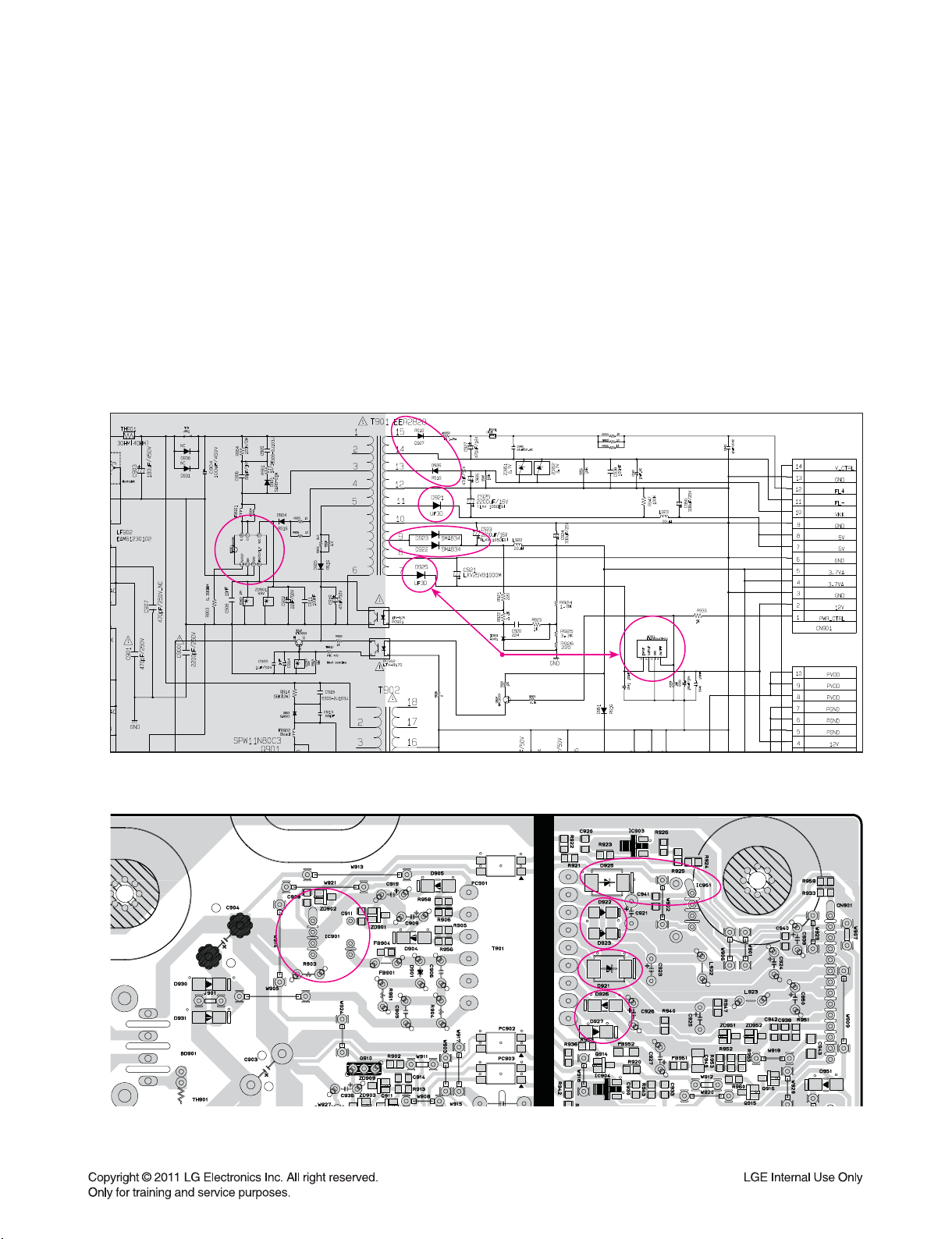
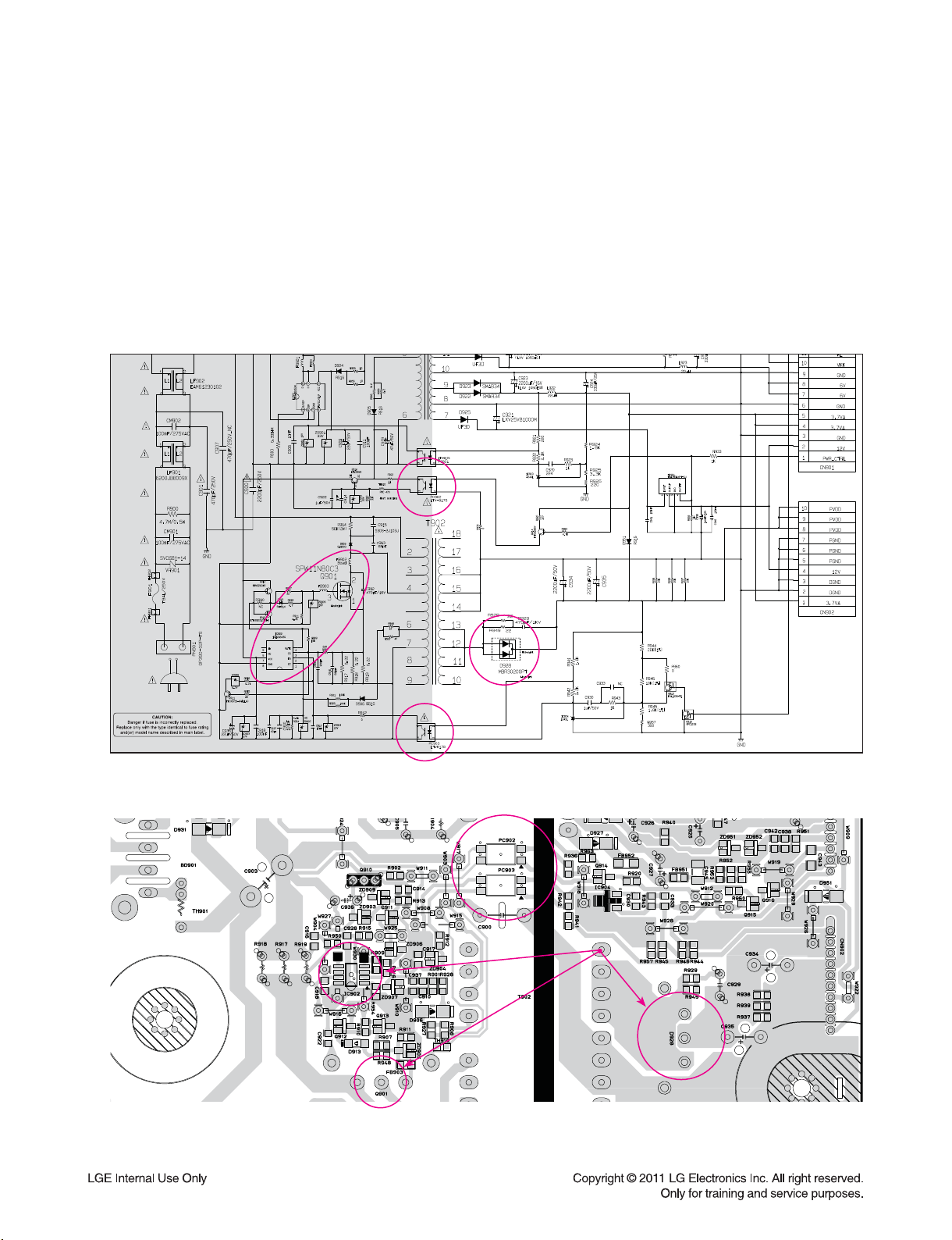
1. SMPS CIRCUIT DIAGRAM
12
11
10
9
8
IMPORTANT SAFETY NOTICE
WHEN SERVICING THIS CHASSIS, UNDER NO
CIRCUMSTANCES SHOULD THE ORIGINAL DESIGN
BE MODIFIED OR ALTERED WITH OUT PERMISSION
FROM THE LG CORPORATION. ALL COMPONENTS
SHOULD BE REPLACED ONLY WITH TYPES
IDENTICAL TO THOSE IN THE ORIGINAL CIRCUIT.
SPECIAL COMPONENTS ARE SHADED ON THE
SCHEMATIC FOR EASY IDENTIFICATION.
THIS CIRCUIT DIAGRAM MAY OCCASIONALLY
DIFFER FROM THE ACTUAL CIRCUIT USED. THIS
WAY, IMPLEMENTATION OF THE LATEST SAFETY
AND PERFORMANCE IMPROVEMENT CHANGES
INTO THE SET IS NOT DELAYED UNTIL THE NEW
SERVICE LITERATURE IS PRINTED.
NOTE :
1. Shaded( ) parts are critical for safety. Replace only
with specified part number.
2. Voltages are DC-measured with a digital voltmeter
during Play mode.
7
6
5
4
3
2
1
A
Warning
Parts that are shaded are critical with
respect to risk of fire or electrical shock.
B C D E F G H I J K L M N O P Q R ST
EBY61190341, REV4.1
SMPS
2011.01.28
2-362-35
Page 45

2. AUDIO MICOM CIRCUIT DIAGRAM
12
11
10
1
9
8
7
6
5
4
3 24
6 7 5
3
2
1
: WAVEFORM NUMBER
A
B C D E F G H I J K L M N O P Q R ST
EBY61190301(#2), REV5.4
AUDIO MICOM
2011.01.28
2-382-37
Page 46

3. AUDIO DSP CIRCUIT DIAGRAM
12
11
10
9
8
7
10
9
6
5
4
3
2
13
11
12
1
: WAVEFORM NUMBER
A
B C D E F G H I J K L M N O P Q R ST
EBY61190301(#3), REV5.4
AUDIO DSP
2011.01.28
2-402-39
Page 47

4. HDMI CIRCUIT DIAGRAM
12
11
10
9
8
7
6
5
4
8
3
2
1
: WAVEFORM NUMBER
A
B C D E F G H I J K L M N O P Q R ST
EBY61190301(#4), REV5.4
HDMI
2011.01.28
2-422-41
Page 48

5. ADC / DIR CIRCUIT DIAGRAM
12
11
10
9
8
7
6
5
4
3
14
2
1
: WAVEFORM NUMBER
A
B C D E F G H I J K L M N O P Q R ST
EBY61190301(#5), REV5.4
ADC/DIR
2011.01.28
2-442-43
Page 49

6. MCS CIRCUIT DIAGRAM
12
11
10
9
8
16
17
7
6
5
18
15
4
3
2
1
: WAVEFORM NUMBER
A
B C D E F G H I J K L M N O P Q R ST
EBY61190301(#6), REV5.4
MCS
2011.01.28
2-462-45
Page 50

7. PWM CIRCUIT DIAGRAM
12
11
10
9
8
7
6
5
19
4
3
2
1
: WAVEFORM NUMBER
A
B C D E F G H I J K L M N O P Q R ST
EBY61190311(#1), REV3.1
PWM
2011.01.28
2-482-47
Page 51

8. AMP CIRCUIT DIAGRAM
12
11
10
9
8
7
6
5
4
3
2
1
EBY61190311(#2), REV3.1
A
B C D E F G H I J K L M N O P Q R ST
AMP
2011.01.28
2-502-49
Page 52

9. FRONT CIRCUIT DIAGRAM
12
11
10
9
8
7
6
5
4
3
2
1
A
B C D E F G H I J K L M N O P Q R ST
FRONT-VFD
EBY61190321, REV3.3
2011.01.28
2-522-51
Page 53

10. VOLUME CIRCUIT DIAGRAM
12
11
10
9
8
MEMO
7
6
5
4
3
2
1
A
B C D E F G H IJ
FRONT-VOLUME
EBY61190331, REV2.1
2011.01.28
2-542-53
Page 54

CIRCUIT VOLTAGE CHART
Pin No. Desc. Voltage EE Mode
IC100 UPD78F1164 (TOP)
30 EVDD1 3.45 3.52
47 AVREF1 3.45 3.52
50 AVREF0 3.45 3.52
99 VDD 3.45 3.52
100 EVDD0 3.45 3.52
IC101 EEPROM
8 VCC 3.45 -
IC103 TJ3966
2 IN 3.7 -
IC200 CS495314
42 VDD1 1.78 0
55 VDD2 1.78 0
83 VDD3 1.78 0
95 VDD4 1.78 0
112 VDD5 1.78 0
125 VDD6 1.78 0
12 VDD7 1.78 0
22 VDD8 1.78 0
50 VDDIO1 3.29 0
62 VDDIO2 3.29 0
73 VDDIO3 3.29 0
89 VDDIO4 3.29 0
100 VDDIO5 3.29 0
120 VDDIO6 3.29 0
8 VDDIO7 3.29 0
28 VDDIO8 3.29 0
IC201 EM638165TSA-6G (BOTTOM)
1 VDD1 3.3 0
3 VDD3 3.3 0
9 VDD9 3.3 0
14 VDD14 3.3 0
27 VDD27 3.3 0
43 VDD43 3.3 0
49 VDD49 3.3 0
IC202 MX25L3205D
8 VDD 3.29 0
IC203 TJ3965DP
2 IN 3.7 -
3 OUT 1.8 -
IC301 MC3501
9 VDD 3.3 0
51 VDD 3.3 0
Pin No. Desc. Voltage EE Mode
IC302 LM29152RS-ADJ
2IN6 -
4 OUT 5 -
IC400 CS5346_ADC (BOTTOM)
5 VLC 3.3 -
14 VA 5 -
36 VLS 3.29 -
46 VD 3.29 -
IC401 CS8422_DIR
4 VA 3.29 0
19 V_REG 3.29 0
22 VL 3.29 0
IC402 74HCT244
20 Vin 3.29 -
IC403 TJ5205-ADJ
1IN6 -
5 OUT 5 -
IC500 MLC9800
2 AVDD33 3.3 0
30 VDD33 3.3 0
51 VDD33 3.3 0
84 VDD33 3.3 0
113 VDD33 3.3 0
115 USBVDD33 3.3 0
IC501 74HCT244
20 Vin 3.29 -
IC503 EM638165TSA-6G (BOTTOM)
1 VDD1 3.3 0
3 VDD3 3.3 0
9 VDD9 3.3 0
14 VDD14 3.3 0
27 VDD27 3.3 0
43 VDD43 3.3 0
49 VDD49 3.3 0
IC504 AZ1117BH-1.2 FIXED
3 Vin 3.3 -
4 Vout 1.2 -
IC505 MX25L3205D (BOTTOM)
8 VDD 3.29 0
IC506 CP2.0B
5 VCC 3.3 -
IC601 AP2128K-ADJTRG1
3 Vin 3.7 -
Pin No. Desc. Voltage EE Mode
4 Vout 3.3 -
IC603 PS9850
16 VDD_IO 3.3 0
24 VDD_IO 3.3 0
29 VDD_IO 3.3 0
32 VDD_IO 3.3 0
35 VDD_IO 3.3 0
40 VDD_IO 3.3 0
48 VDD_IO 3.3 0
IC701 TAS5614A
25 GVDD_C 12 0
26 GVDD_D 12 0
55 GVDD_A 12 0
56 GVDD_B 12 0
30 PVDD_D 36 0
31 PVDD_D 36 0
38 PVDD_C 36 0
39 PVDD_C 36 0
42 PVDD_B 36 0
43 PVDD_B 36 0
50 PVDD_A 36 0
51 PVDD_A 36 0
IC702 TAS5614A
25 GVDD_C 12 0
26 GVDD_D 12 0
55 GVDD_A 12 0
56 GVDD_B 12 0
30 PVDD_D 36 0
31 PVDD_D 36 0
38 PVDD_C 36 0
39 PVDD_C 36 0
42 PVDD_B 36 0
43 PVDD_B 36 0
50 PVDD_A 36 0
51 PVDD_A 36 0
IC703 TAS5614A
25 GVDD_C 12 0
26 GVDD_D 12 0
55 GVDD_A 12 0
56 GVDD_B 12 0
30 PVDD_D 36 0
31 PVDD_D 36 0
38 PVDD_C 36 0
Pin No. Desc. Voltage EE Mode
39 PVDD_C 36 0
42 PVDD_B 36 0
43 PVDD_B 36 0
50 PVDD_A 36 0
51 PVDD_A 36 0
IC800 ADV7622
2 CVDD 1.8 0
21 CVDD 1.8 0
34 CVDD 1.8 0
110 CVDD 1.8 0
129 CVDD 1.8 0
36 TXPVDD 1.78 0
37 TXPLVDD 1.78 0
45 TXAV 1.78 0
55 TXAV 1.78 0
61 DVDD 1.78 0
81 DVDD 1.78 0
93 DVDD 1.78 0
126 DVDD 1.78 0
6 TVDD 3.3 0
12 TVDD 3.3 0
25 TVDD 3.3 0
31 TVDD 3.3 0
114 TVDD 3.3 0
120 TVDD 3.3 0
133 TVDD 3.3 0
139 TVDD 3.3 0
IC802 74HCT244 (BOTTOM)
20 Vin 3.29 -
IC803 AZ1117BH-ADJ
3 Vin 3.3 -
4 Vout 1.8 -
IC804 AZ1117BH-ADJ
3 Vin 3.3 -
4 Vout 1.8 -
IC805 TJ3965ADJ
2 IN 3.7 -
3 OUT 3.3 -
2-562-55
Page 55

PRINTED CIRCUIT BOARD DIAGRAMS
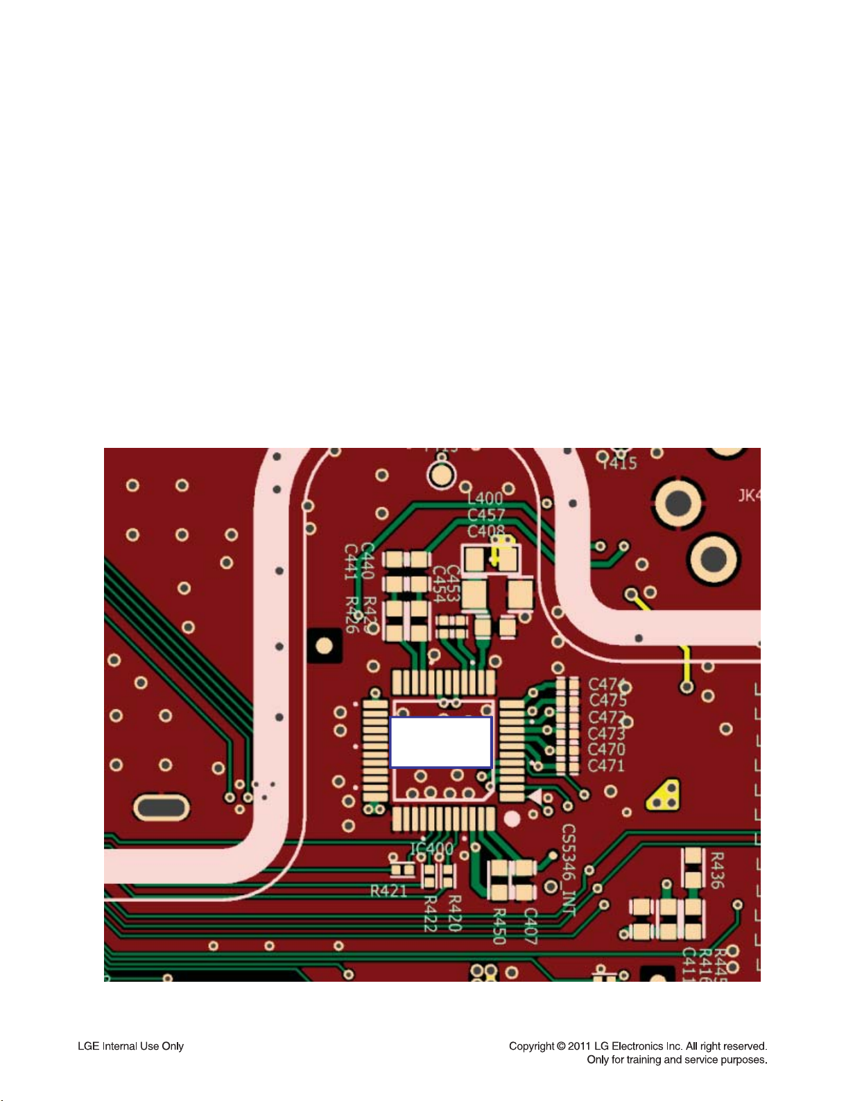
1. MAIN P. C. BOARD
(TOP VIEW)
(BOTTOM VIEW)
2-582-57
Page 56

2. SMPS P. C. BOARD
(TOP VIEW) (BOTTOM VIEW)
NOTE) Warning
Parts that are critical with respect to risk
of fire or electrical shock.
2-602-59
Page 57

3. AMP P. C. BOARD
(TOP VIEW) (BOTTOM VIEW)
2-622-61
Page 58

4. FRONT P. C. BOARD
(TOP VIEW)
(BOTTOM VIEW)
2-642-63
Page 59

5. VOLUME P. C. BOARD
(TOP VIEW)
MEMO
(BOTTOM VIEW)
2-662-65
Page 60

SECTION 3
CABINET & MAIN CHASSIS
CONTENTS
EXPLODED VIEWS ......................................................................................................................................... 3-3
1. CABINET AND MAIN FRAME SECTION ................................................................................................. 3-3
2. SPEAKER SECTION ................................................................................................................................ 3-7
2-1. CENTER SPEAKER EXPLODED VIEW ............................................................................................. 3-7
2-2. FRONT SPEAKER EXPLODED VIEW ............................................................................................... 3-8
2-3. REAR SPEAKER EXPLODED VIEW .................................................................................................. 3-9
2-4. PASSIVE SUBWOOFER EXPLODED VIEW .................................................................................... 3-10
3. PACKING ACCESSORY SECTION ....................................................................................................... 3-11
3-1
Page 61

MEMO
3-2
Page 62

EXPLODED VIEWS
1. CABINET AND MAIN FRAME SECTION
462
279
A43
A50
260
452
265
275
CABLE1
B
464
462
D
468
CABLE2
250
A45
AMP
A
B
468
462
468
A46
464
C
CN901
A
C
MAIN
261
261
320
A44
CN902
A47
3-43-3
SMPS
468
D
F
F
300
Page 63

MEMOMEMO
3-63-5
Page 64

2. SPEAKER SECTION
2-1. CENTER SPEAKER EXPLODED VIEW
A700
3-7
Page 65

2-2. FRONT SPEAKER EXPLODED VIEW
A800
3-8
Page 66

2-3. REAR SPEAKER EXPLODED VIEW
A600
3-9
Page 67

2-4. PASSIVE SUBWOOFER EXPLODED VIEW
A900
3-10
Page 68

3. PACKING ACCESSORY SECTION
801 Owner’s manual
823 HDMI cable
825 FM antenna
900 Remote control
803 Packing
808 Batteries
824 AM antenna
827 Optimizer microphone
804 Bag
803 Packing
803B Speaker packing
803A Speaker packing
803D Speaker packing
802 Box
WIRE80 Front Left
WIRE81 Front Right
WIRE70 Center
WIRE90 Subwoofer
WIRE60 Front Left
WIRE61 Front Right
803C Speaker packing
Speaker cables
3-11
Page 69

MEMO
3-12
 Loading...