

Page 1
MODEL: HT303SU(SH33SU-S/W)/HT353SD(SH33SD-S/W)
SERVICE MANUAL
P/NO : AFN33723386 JANUARY, 2008
DVD/CD RECEIVER
SERVICE MANUAL
MODEL: HT303SU(SH33SU-S, SH33SU-W)/
HT353SD(SH33SD-S, SH33SD-W)
Website http://biz.lgservice.com
Internal Use Only
HT303SU
HT353SD
Page 2

1-1
Copyright © 2008 LG Electronics. Inc. All right reserved.
Only for training and service purposes
LGE Internal Use Only
[CONTENTS]
❍ SECTION 1. GENERAL
• SERVICING PRECAUTIONS . . . . . . . . . . . . . . . . . . . . . . . . . . . . . . . . . . . . . . . . . . . . . . 1-2
• ESD PRECAUTIONS . . . . . . . . . . . . . . . . . . . . . . . . . . . . . . . . . . . . . . . . . . . . . . . . . . . . 1-4
• SERVICE INFORMATION FOR EEPROM . . . . . . . . . . . . . . . . . . . . . . . . . . . . . . . . . . . . . 1-5
•
HOW TO UPDATE AUDIO MICOM & DVD PROGRAMS
. . . . . . . . . . . . . . . . . . . . . . . . . . . . . . . . . . . . . 1-7
• SPECIFICATIONS . . . . . . . . . . . . . . . . . . . . . . . . . . . . . . . . . . . . . . . . . . . . . . . . . . . . . . 1-8
❍ SECTION 2. ELECTRICAL PART
• TROUBLESHOOTING GUIDE . . . . . . . . . . . . . . . . . . . . . . . . . . . . . . . . . . . . . . . . . . . . . 2-1
• DETAILS AND WAVEFORMS ON SYSTEM TEST AND DEBUGGING . . . . . . . . . . . . . . .2-13
• INTERNAL BLOCK DIAGRAM OF ICs . . . . . . . . . . . . . . . . . . . . . . . . . . . . . . . . . . . . . . .2-25
• WIRING DIAGRAM . . . . . . . . . . . . . . . . . . . . . . . . . . . . . . . . . . . . . . . . . . . . . . . . . . . . . 2-45
• OVERALL BLOCK DIAGRAM . . . . . . . . . . . . . . . . . . . . . . . . . . . . . . . . . . . . . . . . . . . . 2-47
• CIRCUIT DIAGRAMS . . . . . . . . . . . . . . . . . . . . . . . . . . . . . . . . . . . . . . . . . . . . . . . . . . . 2-49
• PRINTED CIRCUIT DIARGAMS . . . . . . . . . . . . . . . . . . . . . . . . . . . . . . . . . . . . . . . . . . . 2-69
❍ SECTION 3. EXPLODED VIEWS . . . . . . . . . . . . . . . . . . . . . . . . . . . . . . . . . . . . . . . . . 3-1
• CABINET AND MAIN FRAME SECTION . . . . . . . . . . . . . . . . . . . . . . . . . . . . . . . . . . . . . 3-1
• DECK MECHANISM EXPLODED VIEW(DP-12TV) . . . . . . . . . . . . . . . . . . . . . . . . . . . . . . 3-3
• PACKING ACCESSORY SECTION . . . . . . . . . . . . . . . . . . . . . . . . . . . . . . . . . . . . . . . . . . 3-5
• SPEAKER SECTION . . . . . . . . . . . . . . . . . . . . . . . . . . . . . . . . . . . . . . . . . . . . . . . . . . . . 3-6
❍ SECTION 4. MECHANISM (DP-12TV) . . . . . . . . . . . . . . . . . . . . . . . . . . . . . . . . . . . . 4-1
❍ SECTION 5. REPLACEMENT PARTS LIST . . . . . . . . . . . . . . . . . . . . . . . . . . . . . . . . 5-1
Page 3
Copyright © 2008 LG Electronics. Inc. All right reserved.
Only for training and service purposes
LGE Internal Use Only
1-2
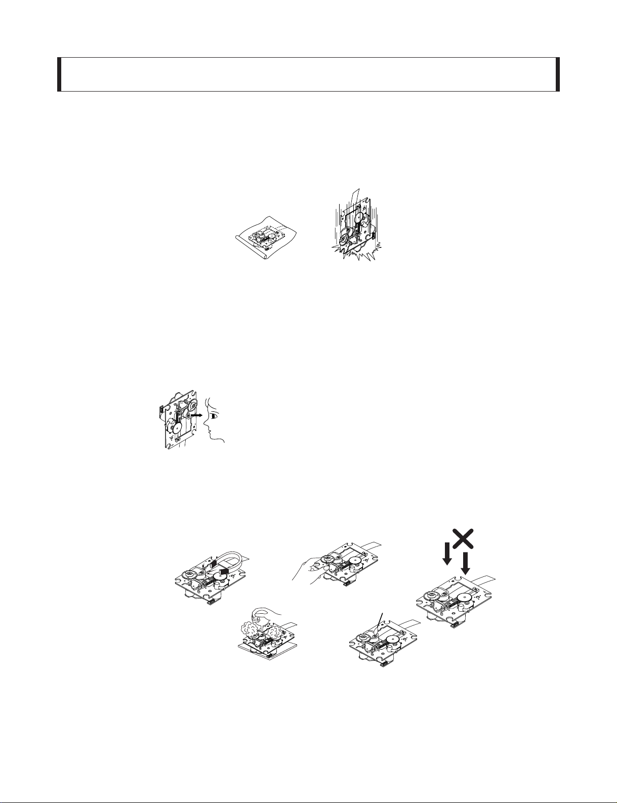
SERVICING PRECAUTIONS
NOTES REGARDING HANDLING OF THE PICK-UP
1. Notes for transport and storage
1) The pick-up should always be left in its conductive bag until immediately prior to use.
2) The pick-up should never be subjected to external pressure or impact.
2. Repair notes
1) The pick-up incorporates a strong magnet, and so should never be brought close to magnetic materials.
2) The pick-up should always be handled correctly and carefully, taking care to avoid external pressure and
impact. If it is subjected to strong pressure or impact, the result may be an operational malfunction and/or
damage to the printed-circuit board.
3) Each and every pick-up is already individually adjusted to a high degree of precision, and for that reason
the adjustment point and installation screws should absolutely never be touched.
4) Laser beams may damage the eyes!
Absolutely never permit laser beams to enter the eyes!
Also NEVER switch ON the power to the laser output part (lens, etc.) of the pick-up if it is damaged.
5) Cleaning the lens surface
If there is dust on the lens surface, the dust should be cleaned away by using an air bush (such as used
for camera lens). The lens is held by a delicate spring. When cleaning the lens surface, therefore, a cotton
swab should be used, taking care not to distort lens.
6) Never attempt to disassemble the pick-up.
Spring has excess pressure. If the lens is extremely dirty, apply isopropyl alcohol to the cotton swab.
(Do not use any other liquid cleaners, because they will damage the lens.) Take care not to use too much
of this alcohol on the swab, and do not allow the alcohol to get inside the pick-up.
Storage in conductive bag
Drop impact
NEVER look directly at the laser beam, and don’t allow
contact with fingers or other exposed skin.
Magnet
How to hold the pick-up
Conductive Sheet
Cotton swab
Pressure
Pressure
SECTION 1. GENERAL
Page 4
1-3
Copyright © 2008 LG Electronics. Inc. All right reserved.
Only for training and service purposes
LGE Internal Use Only
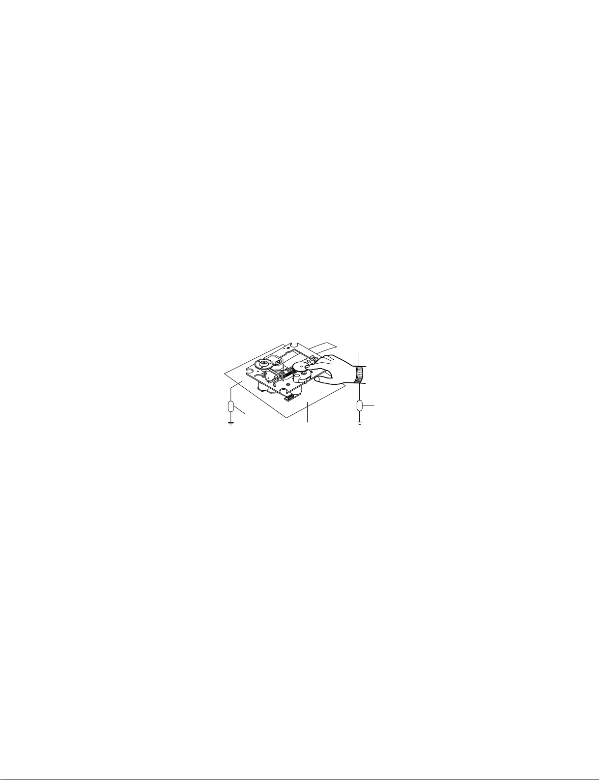
NOTES REGARDING COMPACT DISC PLAYER REPAIRS
1. Preparations
1) Compact disc players incorporate a great many ICs as well as the pick-up (laser diode). These components
are sensitive to, and easily affected by, static electricity. If such static electricity is high voltage, components
can be damaged, and for that reason components should be handled with care.
2) The pick-up is composed of many optical components and other high-precision components. Care must be
taken, therefore, to avoid repair or storage where the temperature or humidity is high, where strong magnetism is present, or where there is excessive dust.
2. Notes for repair
1) Before replacing a component part, first disconnect the power supply lead wire from the unit
2) All equipment, measuring instruments and tools must be grounded.
3) The workbench should be covered with a conductive sheet and grounded.
When removing the laser pick-up from its conductive bag, do not place the pick-up on the bag. (This is
because there is the possibility of damage by static electricity.)
4) To prevent AC leakage, the metal part of the soldering iron should be grounded.
5) Workers should be grounded by an armband (1M Ω)
6) Care should be taken not to permit the laser pick-up to come in contact with clothing, in order to prevent static electricity changes in the clothing to escape from the armband.
7) The laser beam from the pick-up should NEVER be directly facing the eyes or bare skin.
Resistor
(1 Mohm)
Conductive
Sheet
Resistor
(1 Mohm)
Armband
Page 5
1-4
ESD PRECAUTIONS
Electrostatically Sensitive Devices (ESD)
Some semiconductor (solid state) devices can be damaged easily by static electricity. Such components
commonly are called Electrostatically Sensitive Devices (ESD). Examples of typical ESD devices are integrated
circuits and some field-effect transistors and semiconductor chip components. The following techniques should
be used to help reduce the incidence of component damage caused by static electricity.
1. Immediately before handling any semiconductor component or semiconductor-equipped assembly, drain off
any electrostatic charge on your body by touching a known earth ground. Alternatively, obtain and wear a
commercially available discharging wrist strap device, which should be removed for potential shock reasons
prior to applying power to the unit under test.
2. After removing an electrical assembly equipped with ESD devices, place the assembly on a conductive surface
such as aluminum foil, to prevent electrostatic charge buildup or exposure of the assembly.
3. Use only a grounded-tip soldering iron to solder or unsolder ESD devices.
4. Use only an anti-static solder removal device. Some solder removal devices not classified as "anti-static" can
generate electrical charges sufficient to damage ESD devices.
5. Do not use freon-propelled chemicals. These can generate electrical charges sufficient to damage ESD
devices.
6. Do not remove a replacement ESD device from its protective package until immediately before you are
ready to install it. (Most replacement ESD devices are packaged with leads electrically shorted together by
conductive foam, aluminum foil or comparable conductive materials).
7. Immediately before removing the protective material from the leads of a replacement ESD device, touch the
protective material to the chassis or circuit assembly into which the device will by installed.
CAUTION : BE SURE NO POWER IS APPLIED TO THE CHASSIS OR CIRCUIT, AND OBSERVE ALL OTHER
SAFETY PRECAUTIONS.
8. Minimize bodily motions when handing unpackaged replacement ESD devices. (Otherwise harmless motion
such as the brushing together of your clothes fabric or the lifting of your foot from a carpeted floor can generate static electricity sufficient to damage an ESD device).
CAUTION. GRAPHIC SYMBOLS
THE LIGHTNING FLASH WITH APROWHEAD SYMBOL. WITHIN AN EQUILATERAL TRIANGLE, IS
INTENDED TO ALERT THE SERVICE PERSONNEL TO THE PRESENCE OF UNINSULATED
“DANGEROUS VOLTAGE” THAT MAY BE OF SUFFICIENT MAGNITUDE TO CONSTITUTE A RISK OF
ELECTRIC SHOCK.
THE EXCLAMATION POINT WITHIN AN EQUILATERAL TRIANGLE IS INTENDED TO ALERT THE
SERVICE PERSONNEL TO THE PRESENCE OF IMPORTANT SAFETY INFORMATION IN SERVICE
LITERATURE.
Copyright © 2008 LG Electronics. Inc. All right reserved.
Only for training and service purposes
LGE Internal Use Only
Page 6
1-5
Copyright © 2008 LG Electronics. Inc. All right reserved.
Only for training and service purposes
LGE Internal Use Only
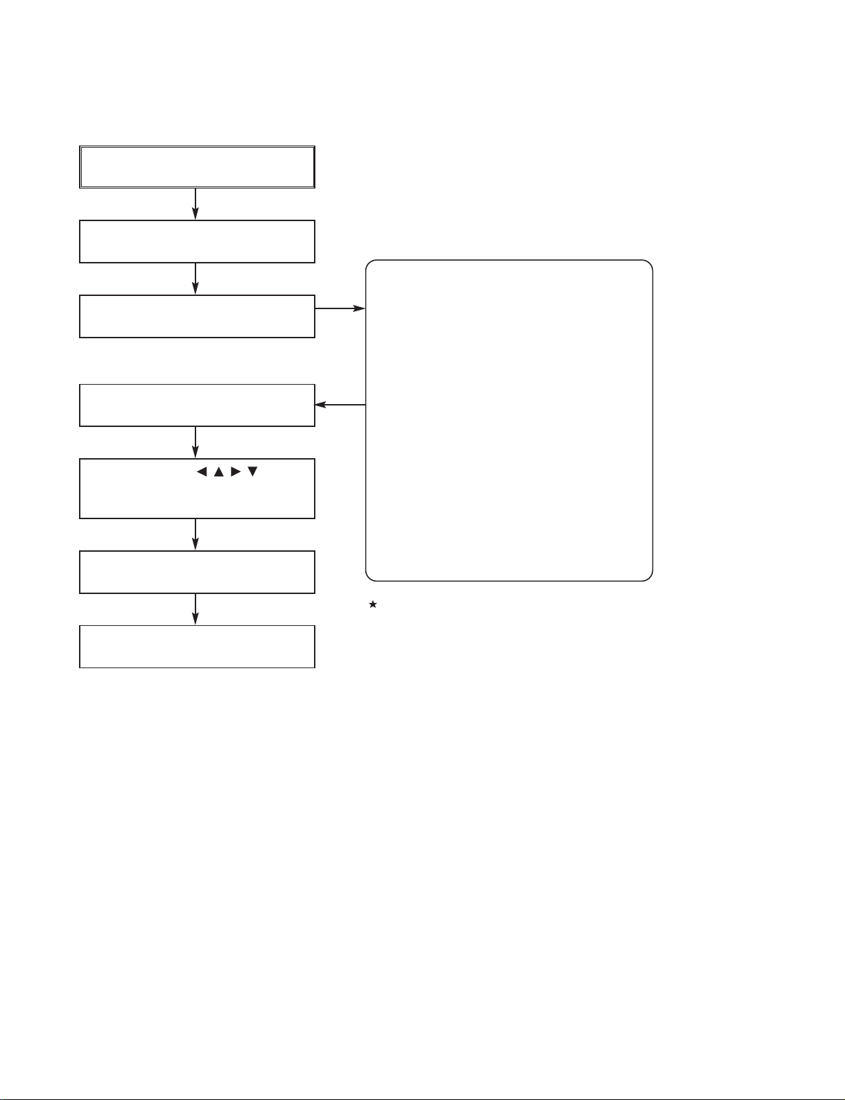
SERVICE INFORMATION FOR EEPROM (DVD PART)
POWER ON
DVD LOGO Status (NO Disk status)
Remote control
Pause key-->1-->4-->7-->2 in order.
Press number 0~9, Press character
A~F (1~6 for a while)
Use arrow key ( ) to
move to appropriate position and
make changes
Press pause key once
Change will be applied when power
OFF-->ON.
DETECT NEW EEPROM
(OPTION EDIT SCREEN)
NAME
OPT 1
OPT 2
OPT 3
OPT 4
OPT 5
OPT 6
OPT 7
OPT 8
OPT 9
OPT A
OPT B
OPT C
OPT D
OPT E
OPT F
OPT G
HEX
44
45
30
FF
22
05
FC
32
AC
00
00
00
00
00
00
00
45
53
11
FF
22
05
FC
32
AC
00
00
00
00
00
00
00
48
55
20
FF
22
05
FC
32
AC
00
00
00
00
00
00
00
52
4F
20
FF
22
05
FC
32
AC
00
00
00
00
00
00
00
<A>
HEX
<B>
HEX
<C>
HEX
<D>
<A> Germany, Austria, Netherlands, France (LGEDG)
<B> Spain, Portugal, Greece, Italy (LGEES)
<C> Hungary, Czech Republic (LGEMK)
<D> Romania (LGERO)
Page 7
Copyright © 2008 LG Electronics. Inc. All right reserved.
Only for training and service purposes
LGE Internal Use Only
1-6
SERVICE INFORMATION FOR EEPROM (AMP PART)
POWER ON
FLD no disc status
Remote control ‘2’ + Front ‘STOP’
push same timing during 5s
FLD ‘OP-0….
Use arrow key ( ) move
to appropriate position and make
changes
Press ENTER key once
FLD ‘write ok’ or ‘up ok’
Remote control ‘2’ + Front ‘STOP’
push same timing
FLD display E2P CLR or EP CLR
Auto power off
MODEL : HT303
NAME HEX
OPT 1 82
OPT 2 CA
OPT 3 21
OPT 4 27
OPT 5 00
MODEL : HT353
NAME HEX
OPT 1 82
OPT 2 CA
OPT 3 20
OPT 4 27
OPT 5 00
DETECT NEW EEPROM
(OPTION EDIT SCREEN)
Page 8

1-7
HOW TO UPDATE AUDIO MICOM & DVD PROGRAMS
Copyright © 2008 LG Electronics. Inc. All right reserved.
Only for training and service purposes
LGE Internal Use Only
1. How to update AUDIO MICOM program.
[Update using CD]
1. Change the filename to download as “(MODEL NAME)_(Version).HEX”. Only upper cases are permitted.
ex) HT353 : “HT353_0709081.HEX”
2. Copy the file to the root folder of a CD and burn it.
3. Insert the CD to the SET, and move to the DVD function. Then the upgrade process will be started with
the upgrade information.
4. If the upgrade process is complete, the set will be rebooted with “Complete” message.
[Update using USB]
1. Change the filename to download as “(MODEL NAME)_(Version).HEX”. Only upper cases are permitted.
ex) HT353 : “HT353_0709081.HEX”
2. Copy the file to the root folder of USB storage.
3. Put the USB into the SET, and move to the USB function. Then the upgrade process will be started with
the upgrade information.
4. If the upgrade process is complete, the set will be rebooted with “Complete” message.
2. How to update DVD program.
[Update using CD]
1. Rename the filename to download as “TARGET.BIN” in upper cases.
2. Copy the file to “\MTK_UPG\” folder of CD, and burn it.
Ex) P:\MTK_UPG\TARGET.BIN
3. Insert the CD to the SET, then after a while the CD tray will be opened with upgrade information on the
screen.
4. Remove the CD, and press UP key in remote controller.
5. Remove and reconnect the power cable when it changes to logo screen from upgrade information. Then
the upgrade process is completed.
[Update using USB]
1. Rename the filename to download as “TARGET.BIN” in upper cases.
2. Copy the file to “\MTK_UPG\” folder of the formatted USB, and burn it.
Ex) P:\MTK_UPG\TARGET.BIN
3. Move to the USB function, and insert the USB to the set. The upgrade information will be shown on the
screen.
4. Remove the USB, press UP key of the remote control.
5. Remove and reconnect the power cable when it changes to logo screen from upgrade information. Then
the upgrade process is completed.
Page 9

1-8
Copyright © 2008 LG Electronics. Inc. All right reserved.
Only for training and service purposes
LGE Internal Use Only
SPECIFICATIONS
(* Depending on the sound mode
settings and the source, there may
be no sound output.)
GENERAL
Power supply Refer to main label
Power consumption Refer to main label
Net Weight 2.5 kg
External dimensions (W x H x D) 360 x 62 x 305 mm
Operating conditions Temperature: 5°C to 35°C, Operation status: Horizontal
Operating humidity 5% to 85%
AMPLIFIER
Output Power Front: 45W + 45W (Rated Output Power 30W, THD 10%)
Center*: 45W
Surround*: 45W + 45W (Rated Output Power 30W, 4 Ωat 1 kHz, THD 10%)
Subwoofer*: 75W (Rated Output Power 60W, 8 Ωat 30 Hz, THD 10%)
SPEAKERS (SH33SU)
Front/Rear/Center Speaker Passive Subwoofer
(SH33SU-S) (SH33SU-W)
Impedance 4Ω 8 Ω
Net Dimensions 99 x 114 x 86 mm 156 x 325 x 320 mm
(W x H x D)
Net Weight (1EA) 0.35 kg 3.5 kg
SPEAKERS (SH33SD)
Front/Rear/Center Speaker Passive Subwoofer
(SH33SD-S) (SH33SD-W)
Impedance 4Ω 8 Ω
Net Dimensions 99 x 114 x 86 mm 156 x 325 x 320 mm
(W x H x D)
Net Weight (1EA) 0.35 kg 3.5 kg
Designs and specifications are subject to change without notice.
Page 10
2-1
Copyright © 2008 LG Electronics. Inc. All right reserved.
Only for training and service purposes
LGE Internal Use Only
SECTION 2. ELECTRICAL PART
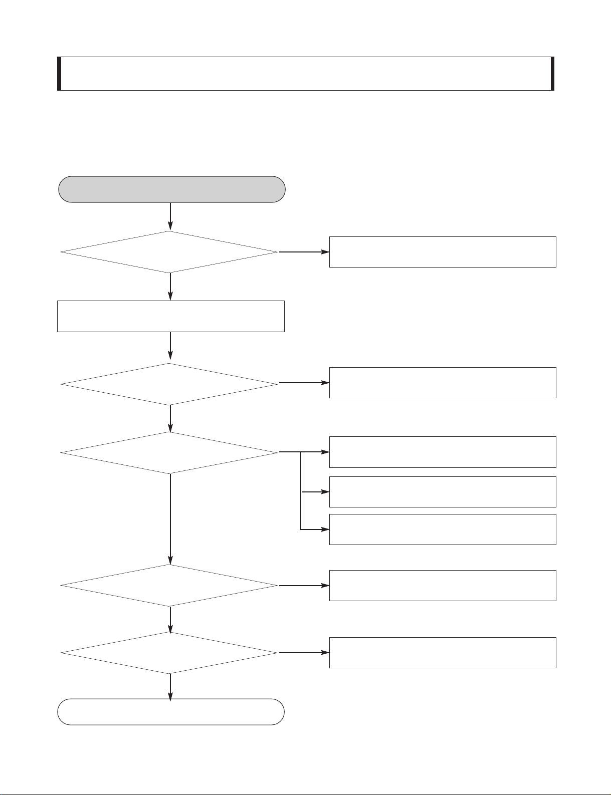
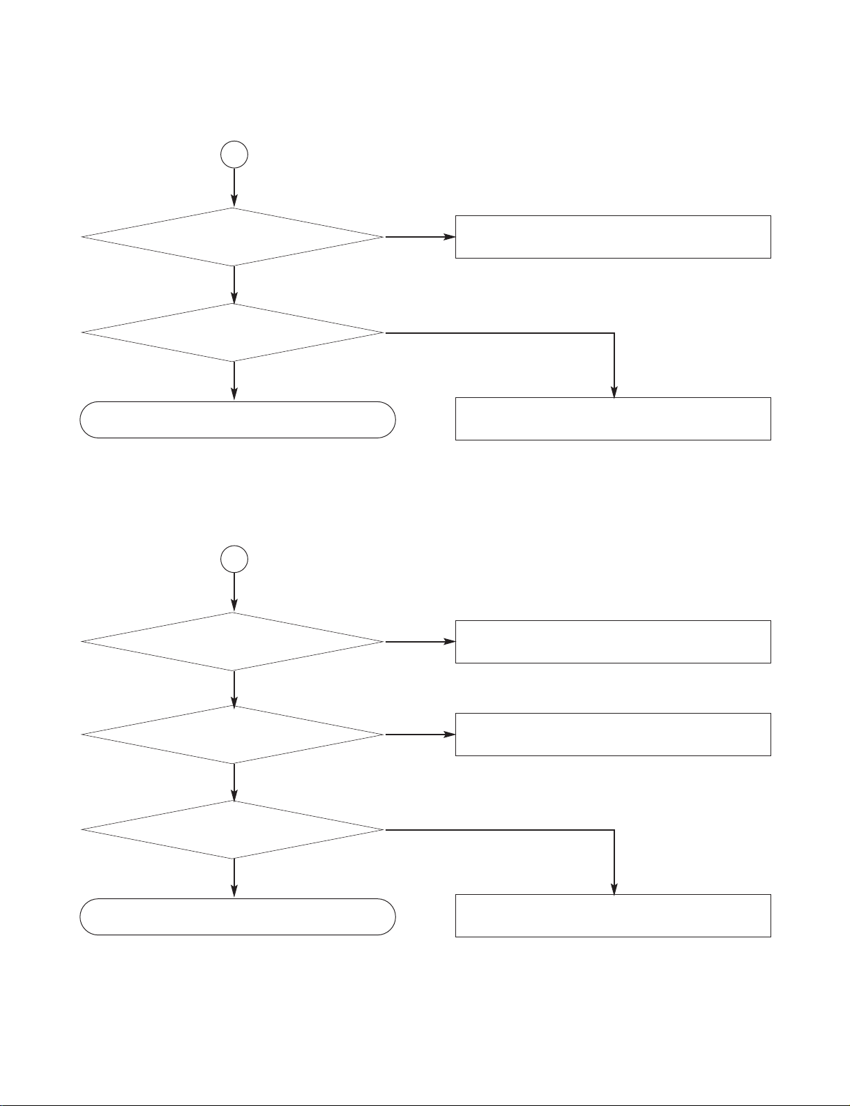
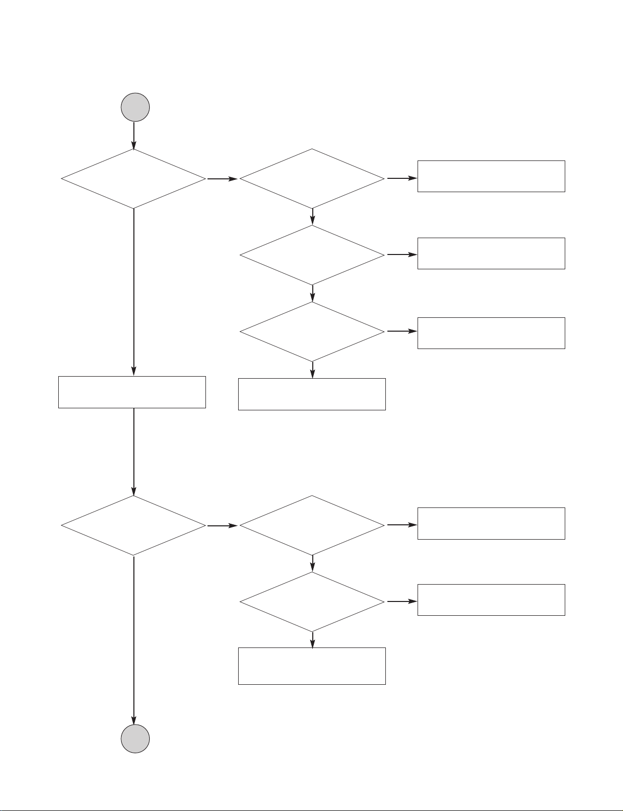
TROUBLESHOOTING GUIDE
1. Power Supply Circuit
YES
NO
Check power plug and power
supply circuit.
NO
Check power supply circuit.
NO
Check laser circuit.
Check focus circuit.
Check disc.
NO
Check tracking servo circuit.
NO
Check audio circuit.
Does red power led
turn on?
YES
Is power on?
YES
Does red power led
turn on?
YES
Does it play?
YES
Does it output
audio?
YES
YES
Turn power on.
INSERT POWER CORD.
OK
Page 11
2-2
Copyright © 2008 LG Electronics. Inc. All right reserved.
Only for training and service purposes
LGE Internal Use Only
2. Front circuit (1/2)
NO NO
Reconnect it.
YES
YES YES
Check if
PN103 is ok?
Red LED turn off?
NO
NO
Refer to SMPS part.
YES
YES
Check if the front
power is ok?
Is the Digitron on
correctly?
NO NO
Check pattern and resoldering
YES
Check if
RC2 is ok?
Check if the remote
control is ok?
YES
Check if all
buttons are ok?
POWER ON.
Front B/D ok.
1
2
Page 12
2-3
Copyright © 2008 LG Electronics. Inc. All right reserved.
Only for training and service purposes
LGE Internal Use Only
3. Front circuit (2/2)
1
NO
Refer to power(SMPS).
NO
Replace R345 ~ R350.
Check if the
power part of the
front is ok?
YES
Check if
R345~R350
ok?
YES
Refer to MICOM circuit.
2
NO
Refer to power(SMPS).
NO
Check RM circuit
Check if the power
part of the front is ok?
YES
NO
Refer to MICOM circuit.
Check if the remote
control waveform of PN301
pin5 is ok?
YES
Check if RC2
voltage is ok(5V)?
YES
Resolder or Replace RC2.
Page 13
Copyright © 2008 LG Electronics. Inc. All right reserved.
Only for training and service purposes
LGE Internal Use Only
2-4
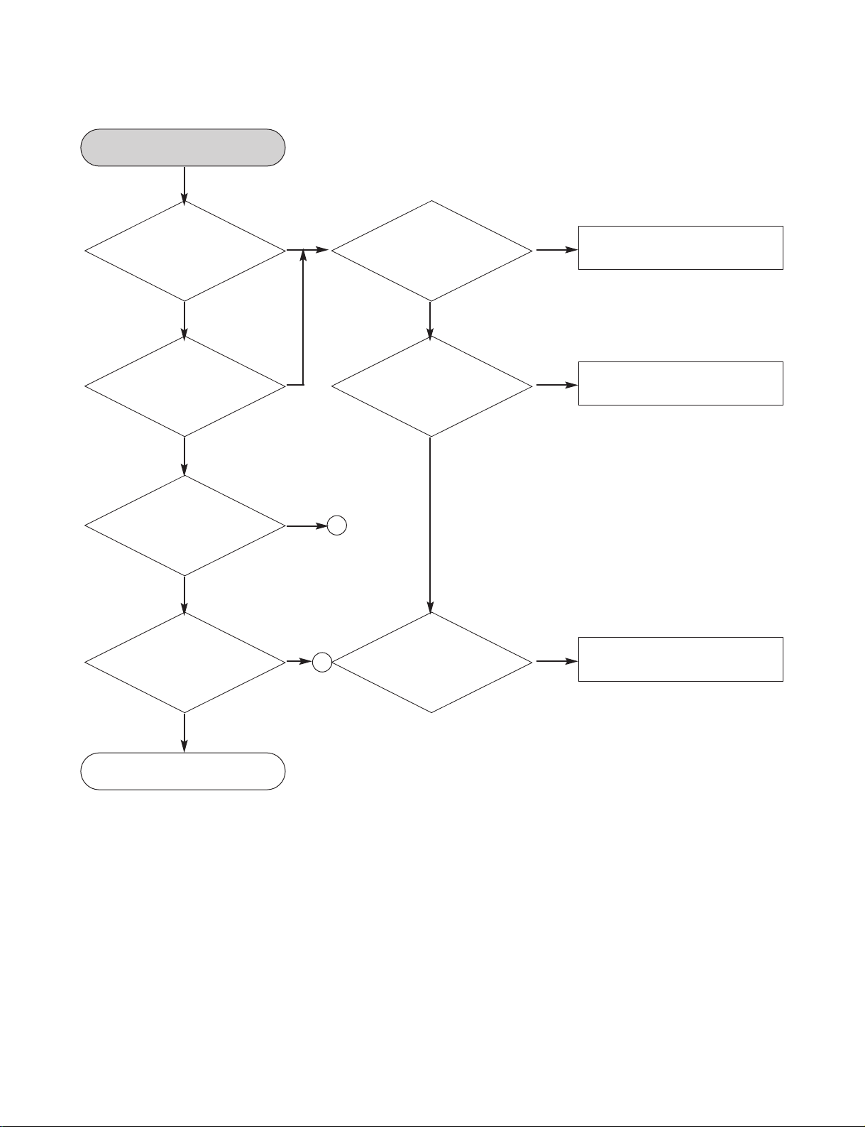
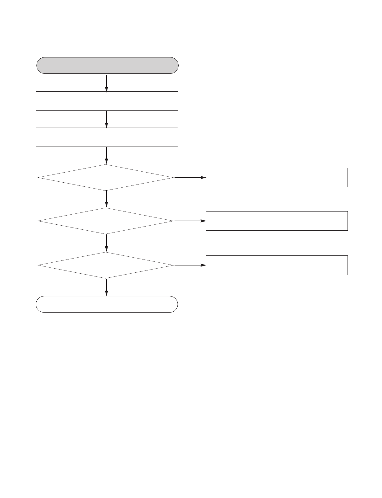
4. System operation flow
YES
YES
YES
Tray closed?
1. Initializes SERVO, DSP & RISC registers.
2. Write RISC code to SDRAM.
3. Reset RISC.
Show LOGO.
Tray close to closed position.
SLED at inner
side?
Recieve
OPEN/ CLOSE
Key?
Receive
CLOSE Key?
SLED moves to inner position.
1. Judge whether have disc and disc type.
2. Jump to related disc reading procedure.
1. Execute Pressed Key & IR Key.
2. System operation routine loop.
NO
NO
NO
NO
YES
1. Stop Playback & Open Tray.
2. Display tray open message & LOGO.
POWER ON.
Page 14
Copyright © 2008 LG Electronics. Inc. All right reserved.
Only for training and service purposes
LGE Internal Use Only
2-5
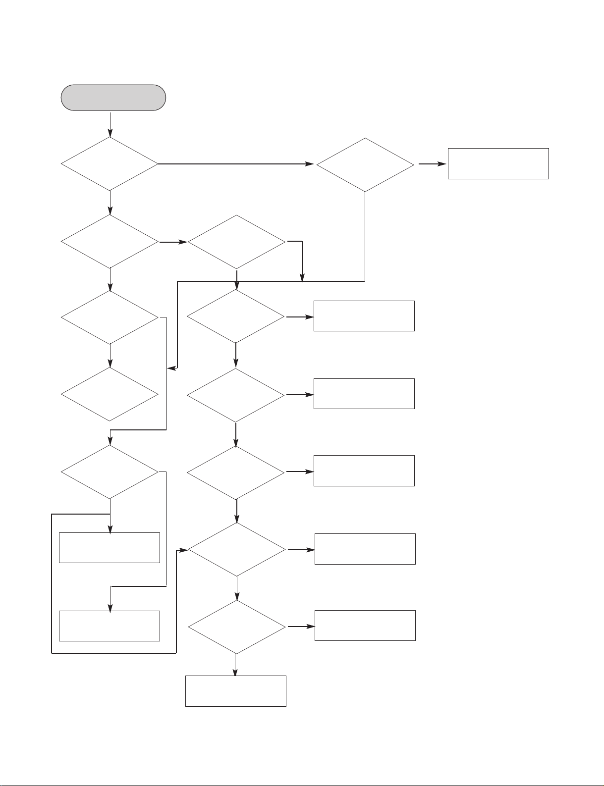
5. Test & debug flow
YES
NO
Check the POWER PART.
NO
Check the POWER PART.
Check the
AC voltage Power PCBA (110V
or 220V).
YES
NO
Check the regulators or diode.
NO
1. Check 27MHz system clock.
2. Check system reset circuit.
3. Check FLASH R/W enable signal PRD,
RWR.
4. Check FLASH Memory related circuit.
NO
Replace FLASH.
Are the
DC Voltage outputs OK? (12V, 5.6V,
3.5V, 5V,7V, 34V).
YES
Are 3.5V and
5V DC outputs normal on main
PCBA?
YES
YES
Update
FLASH successfully?
YES
Switch on the Power PCBA.
TEST.
A
Page 15
Copyright © 2008 LG Electronics. Inc. All right reserved.
Only for training and service purposes
LGE Internal Use Only
2-6
NO
NO
Check connection lines
between FLASH &MT1389/L
and the FLASH access time
whether is suitable or not.
YES
YES
YES
YES
Check AV cable
connection to TV set.
YES
YES
YES
Flash
Memory operates
properly?
NO
Check connection lines
between SDRAM(IC504) &
MT1389/L and the SDRAM
is damaged.
SDRAM
works properly?
NO
Check the related circuit of
MT1389/L IC501 Pins99, 102,
103, 104.
MT1389/L
VIDEO outputs
properly?
Show LOGO?
NO
NO
Check the load OPEN &
CLOSE switch.
Check AV cable connection
between main PCBA and
loader. (MECHA)
YES
YES
YES
Normal
OPEN_SW,
CLOSE_SW
signal?
NO
Check the Tray control IO pins
on MT1389/L.
Normal
IN_SW & OUT_SW
signal?
NO
Check the Tray control MOTOR
& SERVO circuit IC401.
Normal
LOAD+ & LOAD-signal?
Does
Tray move inside when it
is not at closed
position?
Power On.
A
B
Page 16
Copyright © 2008 LG Electronics. Inc. All right reserved.
Only for training and service purposes
LGE Internal Use Only
2-7
NO
NO
Check the connection line of
DRV_MUTE.
YES
YES
YES
Check the cable connection
with MECHA.
Do not put in disc
and close tray.
YES
YES
YES
Motor
Driver DRV_MUTE
pin is high?
NO
Check the related circuit of
SLEGN.
Motor
Driver DRV_MUTE
pin is High?
NO
Check the amp circuit on
motor driver.
SLED+ and
SLED- output
properly?
Does
the SLED move to inner
side when it is at outer
position?
NO
NO
Check Focus connection on
MT1389/L and motor driver.
Check cable connection with
pick-up head.
YES
YES
Proper Focus outputs
to motor dricer?
NO
Check the amp circuit on motor
driver.
Proper F+ & F- outputs?
Optical Lens
has movements for
searching Focus?
B
C
Page 17
Copyright © 2008 LG Electronics. Inc. All right reserved.
Only for training and service purposes
LGE Internal Use Only
2-8
NO
NO
NO
Check the laser power circuit
on MT1389/L and connecting
to power transistor.
(Q401, Q402).
YES
YES
YES
YES
YES
YES
Check cable connection
between transistor output and
pick-up head.
Laser off.
Check the RF connection
between AM5890 and MT1389/L.
YES
YES
DVDLD or
CDLD output
property?
NO
Check the related circuit on
laser power transistor.
Collector
voltage of power transistor
is OK?(Q401, Q402)
Laser turns on when
reading disc?
Put disc in?
NO
NO
Check the SPINDLE related
circuit on MT1389/L.
Check the cable connection
between spindle and main
PCB.
YES
YES
Proper
SPINDLE signal on
MT1389/L.
NO
Check the spindle control amp
circuit of motor driver.
SPNP
SPNN output
properly?
Does spindle rotate?
NO
NO
Check the related circuit on
MT1389/L RF signal.
Proper
RF signal on MT1389/L.
Disc ID is correct?
C
D
Page 18
Copyright © 2008 LG Electronics. Inc. All right reserved.
Only for training and service purposes
LGE Internal Use Only
2-9
NO
NO
Check connections between
MT1389/L and pick-up head.
YES
YES
YES
YES
YES
Check CD_DVDCT connection
between AM5890 and
MT1389/L.
Check cable connection
on pick-up head.
YES
YES
Proper
signals on A, B, C,
D of MT1389/L.
NO
Check the related circuit on
MT1389/L CD-DVDCT.
Proper
CD-DVDCT signal
on MT1389/L.
Focus on ok?
NO
Check RF signal waveform.
Disc Playback?
NO
NO
Check the related circuit on
MT1389/L.
NO
Check the TRACK connection
on MT1389/L and motor driver.
NO
Check the tracking control amp
circuit on motor driver.
Proper
CD-DVDCT signal
on MT1389/L.
YES
Proper
TRACK signal
on MT1389/L.
YES
TR+ & TR-output
properly?
Track On OK?
D
E
Page 19
Copyright © 2008 LG Electronics. Inc. All right reserved.
Only for training and service purposes
LGE Internal Use Only
2-10
NO
NO
Check connection between
IC704 BCK, LRCK, ADATAO.
YES
YES
Check Digital Amp circuit
(IC702, IC703).
YES
YES
PWM IC
received correct data
stream?
NO
Check the related circuit of
PWM.(Check Audio out
Pins 55, 59, 61, 62, 68, 71, 75).
Normal
PWM IC out?(IC704).
Normal Audio
output when disc
playback?
E
TEST END.
Page 20
Copyright © 2008 LG Electronics. Inc. All right reserved.
Only for training and service purposes
LGE Internal Use Only
2-11
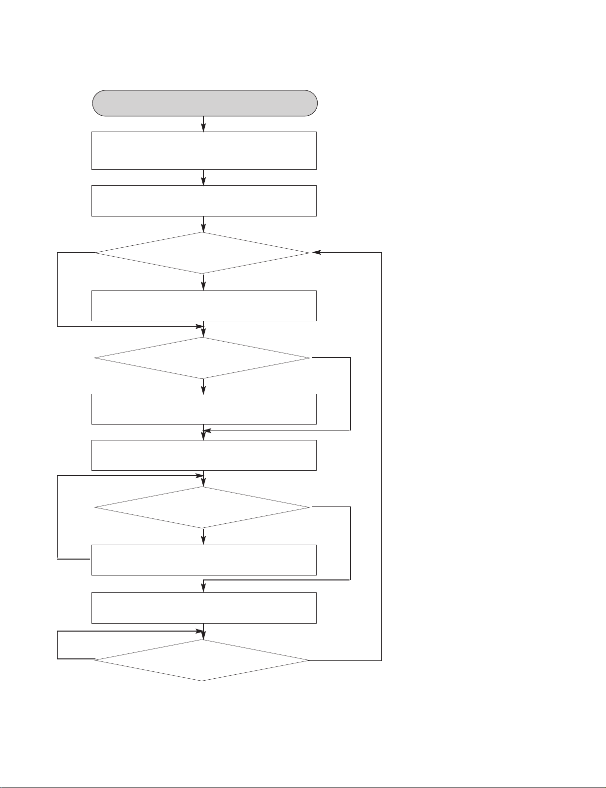
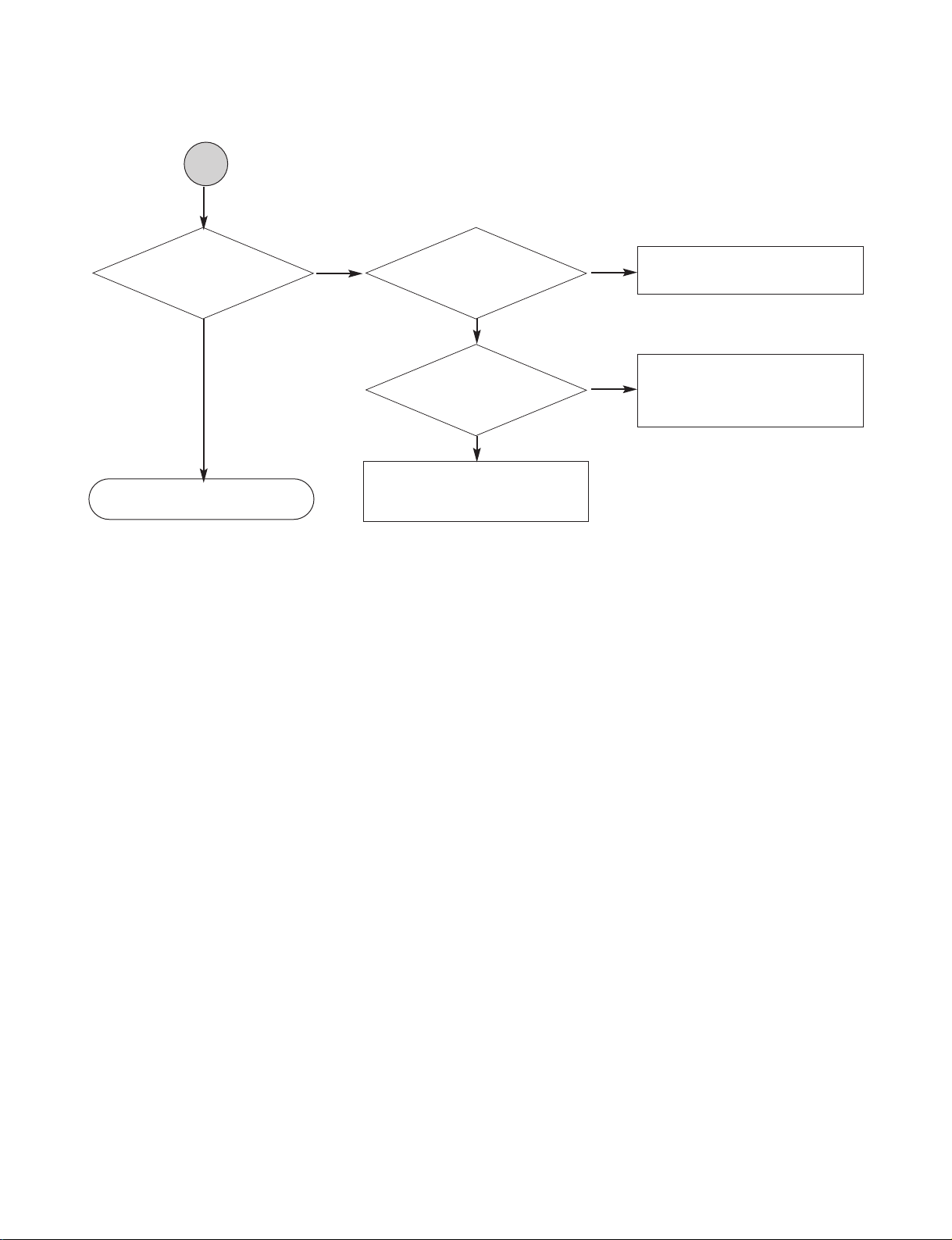
6. AMP Protection
YES
NO
OK.
"PROTECTION"
appears continuously on the FLD.
YES
NO
Replace IC101.
Is the IC101 pin54
"LOW" signal(0V)?
YES
NO
Replace the Q701 and Q702.
Is the Q701 and Q702 normal?
YES
YES
After unplug power cord, connect again.
YES
Power on.
"PROTECTION" appears on the FLD.
Replace ST AMP IC(IC702 and IC703)
Page 21
Copyright © 2008 LG Electronics. Inc. All right reserved.
Only for training and service purposes
LGE Internal Use Only
2-12
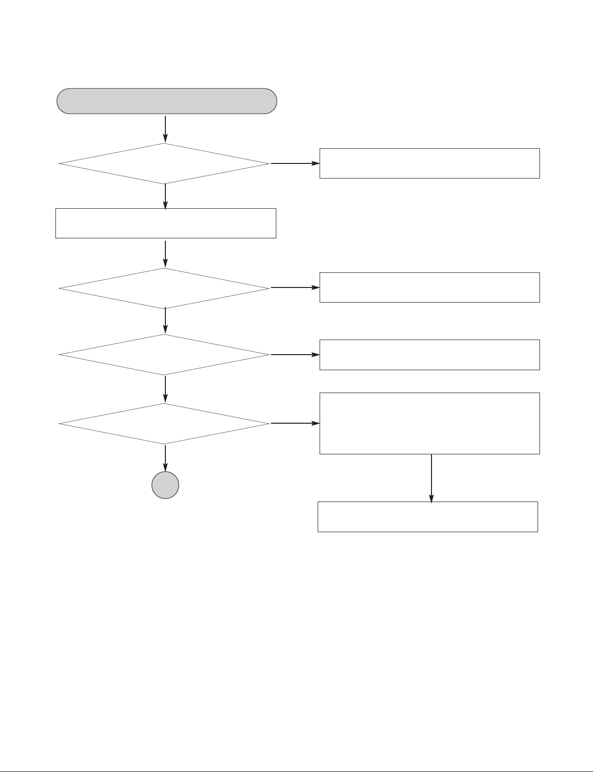
7. AUDIO µ-COM Circuit(DVD & AMP)
Check DVD Module.
Check SMPS.
OK
YES
Power On.
Does
CD/DVD appear at
FLD?
YES
NO
Does
Loading appear
at FLD?
Does
it appear DVD Error
at FLD?
Does Aux,
Scart, opt and FM 87.5
appear at FLD.
YES
Does
no Disc or Time
appear at FLD?
YES
Check
if DVD an audio
micom insert is
OK.
Check Power.
YES
YES
YES
Replace IC101.
YESNO
NO
NO
NO
Refer to SMPS.
NO
Refer to oscillator circuit.
NO
Check IC101 reset
waveform.
NO
NO
YES
Check
power part of Main
B/D.
Check
oscillator o
X101.
Check
if IC101 Pin5
is high.
YES
YES
YES
Check 3.3V line.
NO
Check power section
circuit.
NO
Check
if IC101 Pin9,36,59 are
high(5V).
Check
if IC101 Pin49
is high.
YES
YES
Page 22
Copyright © 2008 LG Electronics. Inc. All right reserved.
Only for training and service purposes
LGE Internal Use Only
2-13
DETAILS AND WAVEFORMS ON SYSTEM TEST AND DEBUGGING
1. SYSTEM 27MHz CLOCK,RESET,FLASH R/W SIGNAL
1)
MT1389/L
main clock is at 27MHz(X501)
1
3 2
4
FIG 1-1
2)
MT1389/L
reset is high active.
Power Cord in
FIG 1-2
1
1
2
3
4
1
2
3
4
IC501
Page 23
Copyright © 2008 LG Electronics. Inc. All right reserved.
Only for training and service purposes
LGE Internal Use Only
2-14
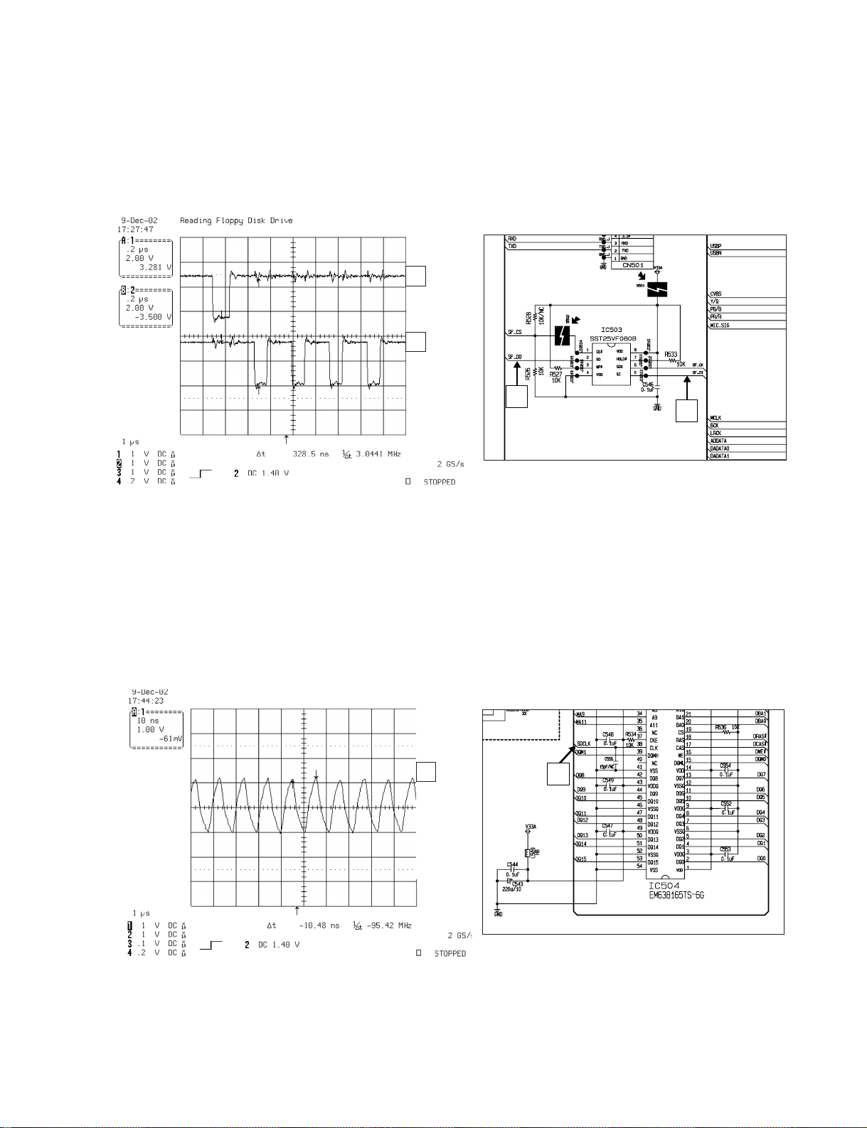
2. SDRAM CLOCK
1)
MT1389/L
main clock is at 27MHz(X501)
DCLK = 93MHz, Vp-p=2.2, Vmax=2.7V
FIG 2-1
3) Flash R/W enable signal during download(Downloading)
FIG 1-4
1
2
1
1
2
1
Page 24
Copyright © 2008 LG Electronics. Inc. All right reserved.
Only for training and service purposes
LGE Internal Use Only
2-15
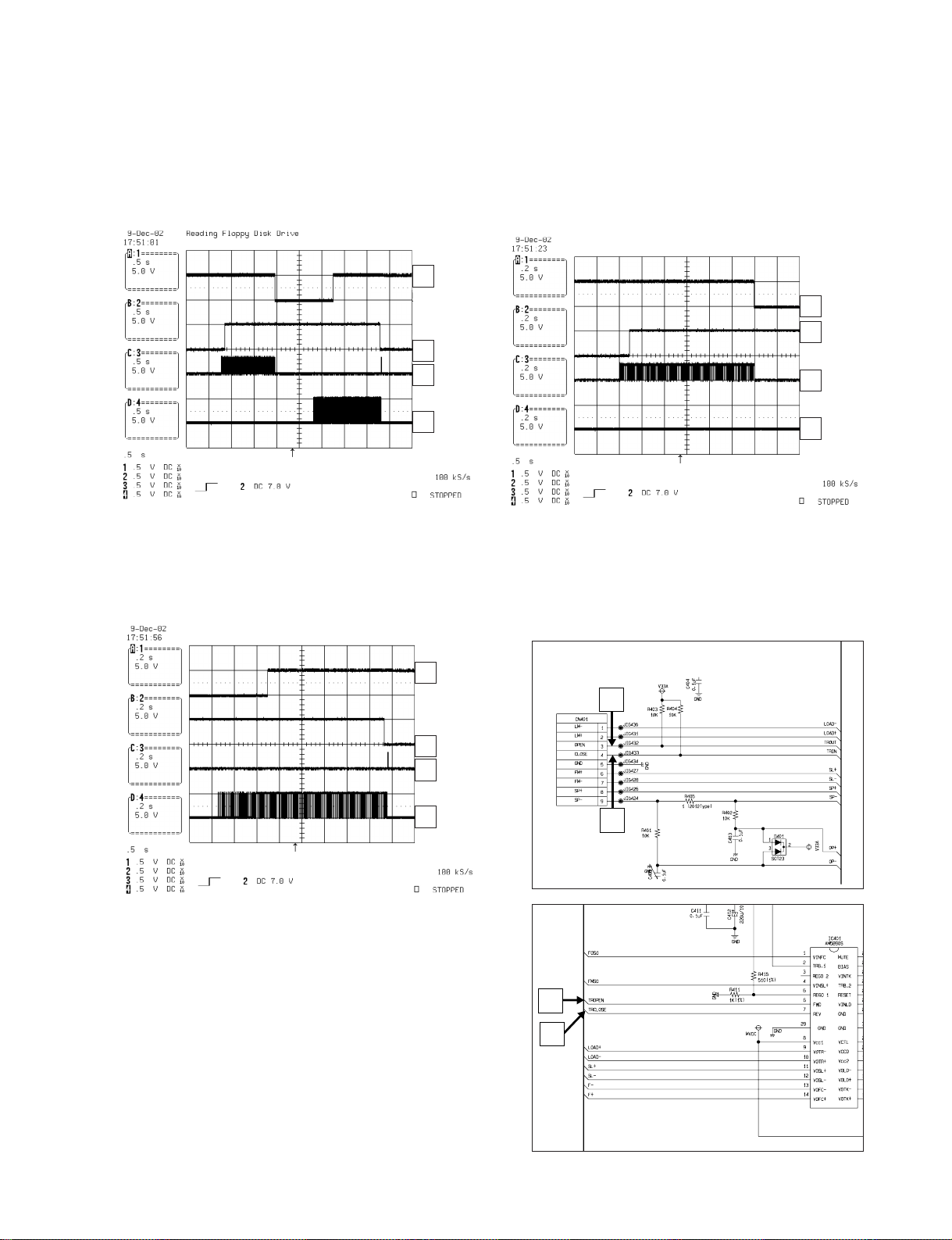
3) Tray open waveform
FIG 3-3
3. TRAY OPEN/CLOSE SIGNAL
1) Tray open/close waveform
FIG 3-1
2) Tray close waveform
FIG 3-2
2
1
3
4
1
2
3
4
1
2
3
4
1
2
3
4
Page 25
Copyright © 2008 LG Electronics. Inc. All right reserved.
Only for training and service purposes
LGE Internal Use Only
2-16
4. SLED CONTROL RELATED SIGNAL (NO DISC CONDITION)
FIG 4-1
1
2
3
4
1
2
3
4
Page 26

Copyright © 2008 LG Electronics. Inc. All right reserved.
Only for training and service purposes
LGE Internal Use Only
2-17
6. LASER POWER CONTROL RELATED SIGNAL(NO DISC CONDITION)
FIG 6-1
5. LENS CONTROL RELATED SIGNAL(NO DISC CONDITION)
FIG 5-1
1
3
2
1
3
2
1
2
3
1
2
3
Page 27

Copyright © 2008 LG Electronics. Inc. All right reserved.
Only for training and service purposes
LGE Internal Use Only
2-18
FIG 7-2 (DVD)
7. DISC TYPE JUDGEMENT WAVEFORMS
FIG 7-1 (DVD)
1
2
3
IC501
IC501
1
2
3
1
2
3
Page 28

Copyright © 2008 LG Electronics. Inc. All right reserved.
Only for training and service purposes
LGE Internal Use Only
2-19
FIG 7-4 (CD)
FIG 7-3 (CD)
1
2
3
IC501
IC501
1
2
3
1
2
3
Page 29

Copyright © 2008 LG Electronics. Inc. All right reserved.
Only for training and service purposes
LGE Internal Use Only
2-20
FIG 8-2 (CD)
8. FOCUS ON WAVEFORMS
FIG 8-1 (DVD)
1
2
3
1
2
3
4
4
1
2
4
3
IC501
Page 30

Copyright © 2008 LG Electronics. Inc. All right reserved.
Only for training and service purposes
LGE Internal Use Only
2-21
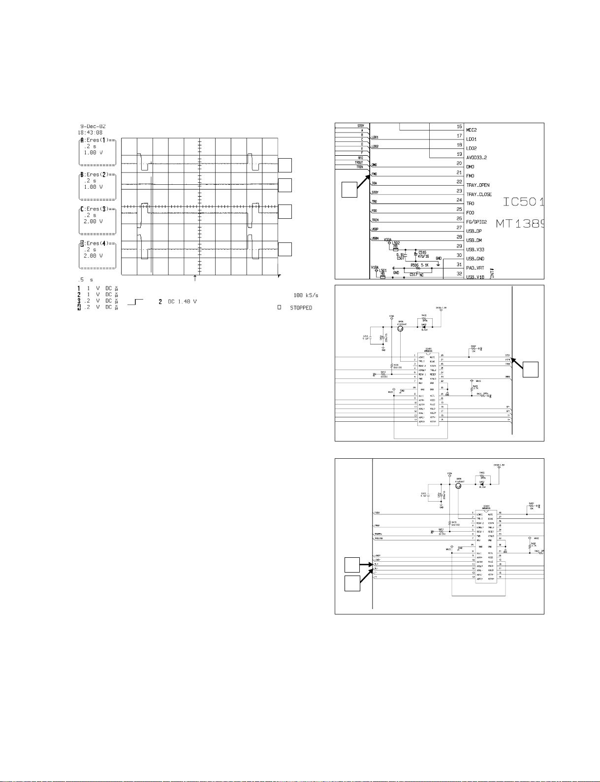
9. SPINDLE CONTROL WAVEFORMS (NO DISC CONDITION)
FIG 9-1
10. TRACKING CONTROL RELATED SIGNAL(System checking)
FIG 10-1(DVD)
1
2
3
1
1
2
3
1
2
3
4
IC501
Page 31

Copyright © 2008 LG Electronics. Inc. All right reserved.
Only for training and service purposes
LGE Internal Use Only
2-22
11.
MT1389/L
VIDEO OUTPUT WAVEFORMS
1) Full colorbar signal(COMPOSIT)
FIG 11-1
FIG 10-2(CD)
3
4
2
1
1
2
4
1
3
Page 32

Copyright © 2008 LG Electronics. Inc. All right reserved.
Only for training and service purposes
LGE Internal Use Only
2-23
ASDATA3
1) Audio related Signal
FIG 12-1
2) Y
FIG 11-2
12. AUDIO OUTPUT FROM mt1389/L
1
1 3 2
IC501
IC501
1
1
2
3
Page 33

Copyright © 2008 LG Electronics. Inc. All right reserved.
Only for training and service purposes
LGE Internal Use Only
2-24
1)
• R703 → TP704
2)
• R720 → TP711
3)
• R704 → TP707
or
R717
→ TP705
4)
• R709 → TP713
5)
• R707 → TP702
6)
• R701 → TP708
13. DVD & AMP WAVEFORMS
6
5
1
4
3
2
Page 34

Copyright © 2008 LG Electronics. Inc. All right reserved.
Only for training and service purposes
LGE Internal Use Only
2-25
GPIO13
DVDD18
GPIO9
XTALI
GPIO8
XTALO
GPIO7 / CKE
V20
V14
REXT
DVSS18
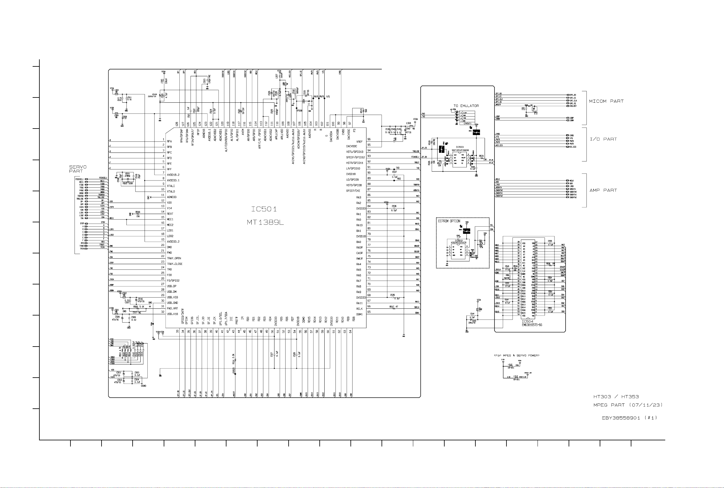
1. IC501 MPEG(MT1389L)
• PIN CONFIGURATION
INTERNAL BLOCK DIAGRAM OF ICs
AKIN1 / GPIO21 / Audio_mute
AKIN2 / GPIO19 / Audio_mute
ALF / CENTER / GPIO
ADVCM / GPIO20 /
DACVDDA
DACVDDB
100
DACVSSC
CVBS
FS
999897
64
APLLVDD
AADVDD
110
109
AADVSS
G
R
B
108
107
106
105
104
103
102
101
ARS / GPIO
AR / GPIO0
116
115
ARF / LFE / GPIO
ADACVSS1
ADACVSS2
APLLCAP
114
113
112
111
RFH / OPINN /
RFIN / OPOUT /
RFG / OPINP /
ADACVDD2
ADACVDD1
ALS / GPIO
AVDD18_1
AGND18
RFIP
128
127
126
125
124
123
122
121
1 96 VREF
RFA
2 95 DACVDDC
RFB
3 94
RFC
4
RFD
5
RFE
6 91
RFF
AVDD18_2
AVDD33_1
AGND33
AVDD33_2
TRAY
_OPEN
TRAY
_CLOSE
FG / GPIO2
USB_DP 27 70 RA8
USB_DM 28 69 RA9
VDD33_USB 29 68 DVDD33
VSS33_USB 30 67 RA11
PAD_VRT 31 66 RCLK
VDD18_USB 32 65 DQM1
7 90
8 89
9 88
10 87
11 86 RA3
12 85 RA2
13 84 DVDD33
14 83 RA1
15 82 RA0
MDI1
16 81 RA10
MDI2
17 80 BA1
LDO1
18
LDO2
19 78 BA0
20 77 RAS#
DMO
21 76 CAS#
FMO
22 75 RW E#
23 74 RA4
24 73 RA5
TRO
25 72 RA6
FOO
26 71 RA7
33343536373839404142434445464748495051525354555657585960616263
AL / GPIO1
AVCM
120
119
118
117
MT1389L
93 SPDIF / GPIO12
92
GPIO11
GPIO10
79
GPIO3 / INT#
GPIO4
GPIO6
SF_CS_
SF_DO
SF_DI
SF_CK
UP1_6 / SCL
UP1_7 / SDA
ICE
PRST#IRRD0
RD1
RD2
RD3
RD4
DVDD33
RD5
RD6
RD7
DVDD18
DQM0
RD15
RD14
RD13
RD12
DVSS33
RD11
RD10
RD9
RD8
Page 35

Copyright © 2008 LG Electronics. Inc. All right reserved.
Only for training and service purposes
LGE Internal Use Only
2-26
1. IC501 MPEG(MT1389L)
• BLOCK DIAGRAM
DVD
PUH
Module
Motor
Drive
FLASH
ROM
DRAM
GPIO
IR/VFD
RF Amplifier
Servo IO
Spindle
Control
Memory
Controller
System
CPU
Debug
Servo
Processor
Audio
DSP
System
Parser
CPPM/CPRM
DRM
32-bit
RISC
Po
rt
108MHz
TV Encoder
Video
Processor
Video DAC
De-
interlacer
MPEG-1/2/4
JPEG
Video Decoder
6ch Au
Internal
dio DACs
PCM output
Audio
Ouptut
CVBS, Y/C
Component
Vide
o
6ch Audio Analog
s
output
Audio
DAC
SDPIF
Audio Mic1
Internal
Audio A
DC
Audio Mic2
USB 2.0 High
Speed
controller
MS/SD/MMC
Card
Controller
USB 2.0 High
/ Full Speed
Devic
e
MS/SD/MMC
Flash Card
Page 36

Copyright © 2008 LG Electronics. Inc. All right reserved.
Only for training and service purposes
LGE Internal Use Only
2-27
1. IC501 MPEG(MT1389L)
• PIN DESCRIPTION
Pin Main Alt. Type Description
Analog I nterface (66)
125 RFIP Analog Input AC coupled DVD RF signal input RFIP
126 RFIN OPOUT Analog Input AC coupled DVD RF signal input RFIN
127 RFG OPINP Analog Input Main beam, RF AC input path
128 RFH OPINN Analog Input Main beam, RF AC input path
1 RFA Analog Input RF main beam input A
2 RFB Analog Input RF main beam input B
3 RFC Analog Input RF main beam input C
4 RFD Analog Input RF main beam input D
5 RFE Analog Input RF sub beam input E
6 RFF Analog Input RF sub beam input E
7 AVDD18_2 Analog power Analog 1.8V power
8 AVDD33_1 Analog power Analog 3.3V power
9 XTALI Input 27MHz crystal input
10 XTALO Output 27MHz crystal output
11 AGND33 Analog Ground Analog Ground
12 V20 Analog output Reference voltage 2.0V
13 V14 Analog output Reference voltage 1.4V
14 REXT Analog Input
Current reference input. It generates reference current for
RF path. Connect an external 15K resistor to this pin and
AVSS
15 MDI1 Analog Input Laser power monitor input
16 MDI2 Analog Input Laser power monitor input
17 LDO1 Analog Output Laser driver output
18 LDO2 Analog Output Laser driver output
19 AVDD33_2 Analog Power Analog 3.3V power
20 DMO Analog Output Disk motor control output. PWM output
21 FMO Analog Output Feed motor control. PWM output
22 TRAY_OPEN Analog Output Tray PWM output/Tray open output
23 TRAY_CLOSE Analog Output Tray PWM output/Tray close output
24 TRO Analog Output
Tracking servo output. PDM output of tracking servo
compensator
25 FOO Analog Output
Focus servo output. PDM output of focus servo
compensator
26 FG GPIO2 Analog
1) Motor Hall sensor input
2) GPIO
27 USB_DP Analog Input USB port DPLUS analog pin
28 USB_DM Analog Input USB port DMINUS analog pin
29 VDD33_USB USB Power USB Power pin 3.3V
30 VSS33_USB USB Ground USB ground pin
31 PAD_VRT Analog Inout USB generating reference current
32 VDD18_USB USB Power USB Power pin 1.8V
95 DACVDDC Power Power
96 VREF Analog Bandgap reference voltage
97 FS Analog Full scale adjustment (suggest to use 560 ohm)
98 DACVSSC Ground Ground pin for video DAC circuitry
99 CVBS Analog Analog composite output
• Abbreviations:
SR: Slew Rate
PU: Pull Up
PD: Pull Down
SMT: Schmitt Trigger
4mA~16mA: Output buffer driving strength.
Page 37

Copyright © 2008 LG Electronics. Inc. All right reserved.
Only for training and service purposes
LGE Internal Use Only
2-28
Pin Main Alt. Type Description
100 DACVDDB Power 3.3V power pin for video DAC circuitry
101 DACVDDA Power 3.3V power pin for video DAC circuitry
102 Y/G Analog Green, Y, SY, or CVBS
103 B/CB/PB Analog Blue, CB/PB, or SC
104 R/CR/PR Analog Red, CR/PR, CVBS, or SY
105 AADVSS Ground Ground pin for 2ch audio ADC circuitry
` 1) Audio ADC input 2
2) MS_CLK set B
3) MCDATA
106 AKIN2 Analog 4) Audio Mute
5) HSYN/VSYN output
6) C5
7) GPIO
1) 2ch audio ADC reference voltageC
107 ADVCM Analog 2) C6
3) GPIO
1) Audio ADC input 1
2) MS_D0 set B
3) Audio Mute
108 AKIN1 Analog
4) HSYN/VSYN output
5) C7
6) GPIO
109 AADVDD Power 3.3V power pin for 2ch audio ADC circuitry
110 APLLVDD3 Power 3.3V Power pin for audio clock circuitry
111 APLLCAP Analog InOut APLL external capacitance connection
112 ADACVSS2 Ground Ground pin for audio DAC circuitry
113 ADACVSS1 Ground Ground pin for audio DAC circuitry
114 ARF / LFE GPIO Analog Output
1) Audio DAC sub-woofer channel output
2) While internal audio DAC not used:
a. ACLK
b. GPIO
115 ARS GPIO Analog Output
1) Audio DAC right Surround channel output
2) While internal audio DAC not used:
a. ABCK
b. GPIO
1) Audio DAC right channel output
2) While internal audio DAC not used:
116 AR Analog Output a. SDATA2
b. GPIO
c. RXD2
117 AV CM Analog Audio DAC reference voltage
118 AL GPIO Analog Output
1) Audio DAC left channel output
2) While internal audio DAC not used:
a. SDATA1
b. GPIO
c. RXD1
119 ALS GPIO Analog Output
1) Audio DAC left Surround channel output
2) While internal audio DAC not used:
a. ALRCK
b. GPIO
120 ALF /CENTER GPIO Analog Output
1) Audio DAC center channel output
2) While internal audio DAC not used:
a. ASDATA0
b. GPIO
121 ADACVDD1 Analog Power 3.3V power pin for audio DAC circuitry
122 ADACVDD2 Analog Power 3.3V power pin for audio DAC circuitry
123 AVDD18_1 Analog Power Analog 1.8V power
124 AGND18 Analog Ground Analog Ground
General Power/ Ground (7)
54, 90 DVDD18 Power 1.8V power pin for internal digital circuitry
Page 38

Copyright © 2008 LG Electronics. Inc. All right reserved.
Only for training and service purposes
LGE Internal Use Only
2-29
Pin Main Alt. Type Description
79 DVSS18 Ground 1.8V Ground pin for internal digital circuitry
50, 68,84
DVDD33 Power 3.3V power pin for internal digital circuitry
60 DVSS Ground 3.3V Ground pin for internal digital circuitry
Micro Controller , Flash I nterface and GPIO(12)
33 GPIO3 INT#
InOut 1) General purpose IO 3
8mA, SR 2) Microcontroller external interrupt 1
PD, SMT
34 GPIO4
InOut
General purpose IO 4
4mA, PD
35 GPIO6
InOut
General purpose IO 6
4mA, PD
36 SF_CS_
InOut
8mA, SR Serial Flash Chip Select
PU, SMT
37 SF_DO
InOut
8mA, SR Serial Flash Dout
PD, SMT
38 SF_DI
InOut
8mA, SR Serial Flash Din
PU, SMT
39 SF_CK
InOut
8mA, SR Serial Flash Clock
PD, SMT
40 UP1_6 SCL
InOut 1) Microcontroller port 1-6
8mA, SR 2) I2C clock pin
PU, SMT
41 UP1_7 SDA
InOut 1) Microcontroller port 1-7
4mA, SR 2) I2C data pin
PU, SMT
42 ICE
Input
Microcontroller ICE mode enable
PD, SMT
43
PRST#
Input
Power on reset input, active low
PU, SMT
44 IR
Input
IR control signal input
SMT
Dram Interface (37) (Sorted by position)
45 RD0
InOut
DRAM data 0
4mA
46 RD1
InOut
DRAM data 1
4mA
47 RD2
InOut
DRAM data 2
4mA
48 RD3
InOut
DRAM data 3
4mA
49 RD4
InOut
DRAM data 4
4mA
51 RD5
InOut
DRAM data 5
4mA
52 RD6
InOut
DRAM data 6
4mA
53 RD7
InOut
DRAM data 7
4mA
55 DQM0
InOut
Data mask 0
4mA, PD
56 RD15
InOut
DRAM data 15
4mA
57 RD14
InOut
DRAM data 14
4mA
58 RD13
InOut
DRAM data 13
4mA
Page 39

Copyright © 2008 LG Electronics. Inc. All right reserved.
Only for training and service purposes
LGE Internal Use Only
2-30
Pin Main Alt. Type Description
59 RD12
InOut
DRAM data 12
4mA
61 RD11
InOut
DRAM data 11
4mA
62 RD10
InOut
DRAM data 10
4mA
63 RD9
InOut
DRAM data 9
4mA
64 RD8
InOut
DRAM data 8
4mA
65 DQM1
InOut
Data mask 1
4mA, PD
66 RCLK
InOut
Dram clock
4mA, PD
67 RA11
InOut
DRAM address bit 11
4mA, PD
69 RA9
InOut
DRAM address 9
4mA, PD
70 RA8
InOut
DRAM address 8
4mA, PD
71 RA7
InOut
DRAM address 7
4mA, PD
72 RA6
InOut
DRAM address 6
4mA, PD
73 RA5
InOut
DRAM address 5
4mA, PD
74 RA4
InOut
DRAM address 4
4mA, PD
75 RWE#
Output
DRAM Write enable, active low
4mA, PD
76 CAS#
Output
DRAM column address strobe, active low
4mA, PD
77 RAS#
Output
DRAM row address strobe, active low
4mA, PD
78 BA0
InOut
DRAM bank address 0
4mA, PD
80 BA1
InOut
DRAM bank address 1
4mA, PD
81 RA10
InOut
DRAM address 10
4mA, PD
82 RA0
InOut
DRAM address 0
4mA, PD
83 RA1
InOut
DRAM address 1
4mA, PD
85 RA2
InOut
DRAM address 2
4mA, PD
86 RA3
InOut
DRAM address 3
4mA, PD
1) GPIO 7
2) Dram Clock Enable
87 GPIO7 CKE
InOut 3) MS_CLK set A
4mA, PD 4) Audio Mute
5) HSYN/VSYN input
6) C0
GPIO (6)
88 GPIO8
1) GPIO8
2) MS_BS set A
InOut 3) SD_CLK set A
4mA, PD 4) ASDATA2
5) ACLK
Page 40

Copyright © 2008 LG Electronics. Inc. All right reserved.
Only for training and service purposes
LGE Internal Use Only
2-31
Pin Main Alt. Type Description
6) Audio Mute
7) HSYN/VSYN input
8) C1
1) GPIO9
2) MS_D0 set A
89 GPIO9
InOut 3) SD_CMD set A
4mA, PD 4) ASDATA1
5) ABCK
6) C2
7) RXD1
1) GPIO10
2) SD_CLK set B
3) SD_D0 set A
91 GPIO10
InOut 4) ASDATA0
4mA, PD 5) ALRCK
6) HSYN/VSYN output
7) C3
8) TXD1
1) GPIO11
2) SD_CMD set B
92 GPIO11
InOut 3) MS_BS set B
4mA, PD 4) Audio Mute
5) HSYN/VSYN output
6) C4
93 SPDIF GPIO12
InOut 1) SPDIF output
2mA, PD 2) GPIO12
1) GPIO13
94 GPIO13
InOut 2) SD_D0 set B
4mA, PD 3) ALRCK
4) Audio Mute
5) YUVCLK
Page 41

Copyright © 2008 LG Electronics. Inc. All right reserved.
Only for training and service purposes
LGE Internal Use Only
2-32
2. IC401 MOTOR DRIVER
• PIN CONFIGURATION
• BLOCK DIAGRAM
Page 42

Copyright © 2008 LG Electronics. Inc. All right reserved.
Only for training and service purposes
LGE Internal Use Only
2-33
1. IC501 MPEG(MT1389L)
• PIN DESCRIPTION
Page 43

Copyright © 2008 LG Electronics. Inc. All right reserved.
Only for training and service purposes
LGE Internal Use Only
2-34
3. IC101 MICOM1389L)
• PIN CONFIGURATION
8
33
3435363738
3940
5
6
P83/AN3
P84/AN4
P85/AN5
P86/AN6
PC0
PC1
PC2
PC3
PC4
PC5/DBGP0
3
PC6DBGP1
DD
PC7/DBGP2
V
3
V
SS
P30
P31
P70/INT0/T0LCP/AN8
P71/INT1/T0HCP/AN9
P72/INT2/T0IN/NKIN
P73/INT3/T0IN
RES
XT1/AN10
XT2/AN11
VSS1
CF1
CF2
VDD1
P80/AN0
P81/AN1
P82/AN2
P10/SO0
P11/SI0/SB0
49
50
51
52
53
54
55
56
57
58
59
60
61
62
63
64
4
47 4
4243444
41
LC87F5M64A
7654123
32
P32/UTX1
31
P33/URX1
30
P34/UTX2
29
P35/URX2
28
P36
27
P37
26
P27/INT5/T1IN
25
P26/INT5/T1IN
24
P25/INT5/T1IN
23
P24/INT5/T1IN/INT7
22
P23INT4/T1IN
21
P22/INT4/T1IN
20
P21/INT4/T1IN
19
P20/INT4/T1IN/INT6
18
P07/T7O
17
P06/T6O
15
141312111098
16
2
2
P00
P01
P02
P03
PWM3
V
P13/SO1
P12/SCK0
P15/SCK1
P14/SI1/SB1
P16/T1PWML
PWM2
P17/T1PWMH/BUZ
SS
DD
V
P04
P05/CKO
Top view
Page 44

Copyright © 2008 LG Electronics. Inc. All right reserved.
Only for training and service purposes
LGE Internal Use Only
2-35
• BLOCK DIAGRAM
SIO
0
SIO
1
Timer 0
Timer 1
Interrupt control
Standby
CF
RC
X’tal
MRC
control
r
Clock
generato
Bus interface
Port 0
Port 1
Port 2
IR PLA
ROM correct
Flash ROM
PC
ACC
B register
C register
Timer 4
Timer 5
Timer 6
Timer 7
Base timer
PWM2/3
Port 7
Port 8
ADC
INT0 to INT7
Noise filter
Port 3
Port C
UART1
UART2
ALU
PSW
RAR
RAM
Stack pointer
Watchdog timer
On-chip Debugger
Page 45

Copyright © 2008 LG Electronics. Inc. All right reserved.
Only for training and service purposes
LGE Internal Use Only
2-36
3. IC101 MICOM
• PIN DESCRIPTION
Pin Name I/O Description Option
VSS1, VSS2
VSS3
VDD1, VDD2
VDD3
Port 0
P00 to P07
Port 1
P10 to P17
Port 2 • 8-bit I/O port
P20 to P27
- - Power supply pin
- + Power supply pin
I/O • 8-bit I/O port
• I/O specifiable in 4-bit units
• Pull-up resistor can be turned on and off in 4-bit units
• HOLD release input
• Port 0 interrupt input
• Shared Pins
P05 : Clock output (system clock / can selected from sub clock)
P06 : Timer 6 toggle output
P07 : Timer 7 toggle output
I/O • 8-bit I/O port
• I/O specifiable in 1-bit units
• Pull-up resistor can be turned on and off in 1-bit units
• Pin functions
P10 : SIO0 data output
P11 : SIO0 data input/bus I/O
P12 : SIO0 clock I/O
P13 : SIO1 data output
P14 : SIO1 data input/bus I/O
P15 : SIO1 clock I/O
P16 : Timer 1 PWML output
P17 : Timer 1 PWMH output/beeper output
I/O Ye
• I/O specifiable in 1-bit units
• Pull-up resistor can be turned on and off in 1-bit units
• Other functions
P20: INT4 input/HOLD reset input/timer 1 event input/timer 0L capture input/
timer 0H capture input/INT6 input/timer 0L capture 1 input
P21 to P23 : INT4 input/HOLD reset input/timer 1 event input/timer 0L capture input/
timer 0H capture input
P24: INT5 input/HOLD reset input/timer 1 event input/timer 0L capture input/
timer 0H capture input/INT7 input/timer 0H capture 1 input
P25 to P27: INT5 input/HOLD reset input/timer 1 event input/timer 0L capture input/
timer 0H capture input
• Interrupt acknowledge ty
INT4
INT5
INT6
INT7
pe
Rising Falling
enable
enable
enable
enable
enable
enable
enable
enable
Rising/
Falling
enable
enable
enable
enable
H level L lev
disable
disable
disable
disable
disable
disable
disable
disable
el
No
No
Yes
Ye
s
s
Page 46

Copyright © 2008 LG Electronics. Inc. All right reserved.
Only for training and service purposes
LGE Internal Use Only
2-37
Pin Name I/O Description Option
Port 7 • 4-bit I/O port
P70 to P73
I/O
• I/O specifiable in 1-bit units
• Pull-up resistor can be turned on and off in 1-bit units
• Shared pins
P70 : INT0 input/HOLD reset input/timer 0L capture input/watchdog timer output
P71 : INT1 input/HOLD reset input/timer 0H capture input
P72 : INT2 input/HOLD reset input/timer 0 event input/timer 0L capture input/
high speed clock counter input
P73 : INT3 input (with noise filter)/timer 0 event input/timer 0H capture input
AD converter input port: AN8 (P70), AN9 (P71)
• Interrupt acknowledge ty
INT0 enable enable disable enable
INT1 enable enable disable enable
INT2 enable enable enable disable
INT3 enable enable enable disable
pe
Rising Falling
Rising/
Falling
H level L lev
enable
enable
disable
disable
el
No
Port 8
P80 to P86
PWM2
PWM3
Port 3
P30 to P37
Port C
PC0 to PC7
RES
XT1 Input • 32.768kHz crystal oscillator input pin
XT2 I/O • 32.768kHz crystal oscillator output pin
CF1 Input Ceramic resonator input pin
CF2 Output Ceramic resonator output pin
I/O • 7-bit I/O port
• I/O specifiable in 1-bit units
• Shared pins
AD converter input port : AN0 (P80) to AN6 (P86)
I/O • PWM2 and PWM3 output ports
• General-purpose I/O available
I/O • 8-bit I/O port
• I/O specifiable in 1-bit units
• Pull-up resistor can be turned on and off in 1-bit units
• Pin functions
P32: UART1 transmit
P33: UART1 receive
P34: UART2 transmit
P35: UART2 receive
I/O • 8-bit I/O port
• I/O specifiable in 1-bit units
• Pull-up resistor can be turned on and off in 1-bit units
• Pin functions
PC5 to PC7: On-chip Debugger
Input Reset pin
• Shared pins
General-purpose input port
AD converter input port : AN10
Must be connected to VDD1 if not to be used.
• Shared pins
General-purpose I/O port
AD converter input port : AN11
Must be set for oscillation and kept open if not to be used.
No
No
Ye
Ye
No
No
No
No
No
s
s
Page 47
Copyright © 2008 LG Electronics. Inc. All right reserved.
Only for training and service purposes
LGE Internal Use Only
2-38
4. IC201 ADC(CS5345)
• PIN CONFIGURATION
1
2
3
4
5
6
7
8
9
10
11
12
13 14 15 16 17 18 19 20 21 22 23 24
48 47 46 45 44 43 42 41 40 39 38 37
36
35
34
33
32
31
30
29
28
27
26
25
VLSSDA/CDOUT
AGND
OVFL
SCL/CCLK
AD0/CS
AD1/CDIN
VLC
RESE
T
AIN3A
AIN3B
AIN2A
AIN2B
AIN1A
AIN1B
VA
AFILTB
VQ
TSTO
FILT+
TSTO
AIN4A/MICIN1
AIN4B/MICIN2
AIN5A
AIN5B
AFILTA
TSTO
NC
NC
AGND
AGND
VA
PGAOUTB
PGAOUTA
AIN6B
AIN6A
MICBIAS
INT
VD
DGND
MCLK
LRCK
SCLK
SDOUTNCNC
NC
TSTI
CS5345
Page 48

Copyright © 2008 LG Electronics. Inc. All right reserved.
Only for training and service purposes
LGE Internal Use Only
2-39
4. IC201 ADC(CS5345)
• BLOCK DIAGRAM
.3V to +5V
+3
10
µF
0.1 µF
0.1 µF
0.1 µF
10
µF
+3.3V to +5V
+1.8V
to +
+1.8V
to +
5V
5V
Digital Audio
Capture
Micro-
Controller
See Note 1
2 k
VA
PGAOUT
PGAOUT
AIN1A
AIN1B
AIN2A
A
3.3 µF
B
3.3 µF
1800 pF
1800 pF
1800 pF
100
10 µF
*
*
10 µF
100
100
10 µF
*
Left Analog Inpu
100 k
100 k
Right Analog Inpu
Left Analog Inpu
100 k
t 1
t 1
t 2
0.1 µF
VLS
MCLK
SCLK
LRCK
SDOUT
T
IN
OVFL
VD
VA
RESET
*
SCL/CCLK
SDA/CDOUT
AD1/CDIN
AIN2B
AIN3A
1800 pF
1800 pF
AD0/CS
2 k
C
VL
AIN3B
AIN4A/MICIN1
0.1 µF
AIN4B/MICIN2
1800 pF
1800 pF
1800 pF
10 µF
100
100
10 µF
*
*
10 µF
100
100
10 µF
*
*
10 µF
100
100 k
Right Analog Inpu
Left Analog Inpu
100 k
100 k
Right Analog Inpu
Left Analog Inpu
100 k
100 k
Right Analog Inpu
t 2
t 3
t 3
t 4
t 4
Note 1: Resistors are required
for IC control port operation
NC
NC
NC
NC
NC
Note 2 The value of R
dictated by the microphone
carteridge.
is
L
TSTI
TSTO
TSTO
TST
VQ
FILT+
10 µF
0.1
µF
47 µF
0.1
µF
AG
ND
AIN5A
AIN5B
AINA
O
AIN6B
1800 pF
1800 pF
1800 pF
1800 pF
*
*
*
*
MICBIAS
AGN
D
AGND
**
AFILTA
10 µF
10 µF
10 µF
10 µF
47 µF
2.2nF
100
100
100
100
See Note 2
R
L
2.2nF
Left Analog Inpu
100 k
100 k
Right Analog Inpu
Left Analog Inpu
100 k
100 k
Right Analog Inpu
t 5
t 5
t ;
t 6
AFILTB
DGND
* Capacitors must be C0G or equivalent
Page 49

Copyright © 2008 LG Electronics. Inc. All right reserved.
Only for training and service purposes
LGE Internal Use Only
2-40
Pin Name # Pin Descr iptio n
SDA/CDOUT 1
Serial Control Data (Input/Output) - SDA is a data I/O in IC
®
Mode. CDOUT is the output data line for
the control port interface in SPI
TM
Mode.
SCL/CCLK 2 Serial Control Port Clock (Input) - Serial clock for the serial control port.
AD0/CS 3
Address Bit 0 (IC) / Co ntrol Por t Chip Select (SPI) (Input) - AD0 is a chip address pin in IC Mode;
CS is the chip-select signal for SPI format.
AD1/CDIN 4
Address Bit 1 (IC) / Ser i al Control Dat a Input (SPI) (Input) - AD1 is a chip address pin in IC Mode;
CDIN is the input data line for the control port interface in SPI Mode.
VLC 5
Control Port Power (Input) - Determines the required signal level for the control port interface. Refer
to the Recommended Operating Conditions for appropriate voltages.
RESET 6 Res et (Input) - The device enters a low-power mode when this pin is driven low.
AIN3A
AIN3B
78Stereo Analog Input 3 (Input) - The full-scale level is specified in the ADC Analog Characteristics
specification table.
AIN2A
AIN2B
910Stereo Analog Input 2 (Input) - The full-scale level is specified in the ADC Analog Characteristics
specification table.
• PIN DESCRIPTION
AIN1A
AIN1B
AGND 13 Analog Ground (Input) - Ground reference for the internal analog section.
VA 1 4 Analog Power (Input) - Positive power for the internal analog section.
AFILTA 15 Antialias Filter Connection (Output) - Antialias filter connection for the channel A ADC input.
AFILTB 16 Antialias Filter Connection (Output) - Antialias filter connection for the channel B ADC input.
VQ 17 Quiescent Voltage (Output) - Filter connection for the internal quiescent reference voltage.
TSTO 18 Test Pin (Output) - This pin must be left unconnected.
FILT+ 19 Positive Voltage Reference (Output) - Positive reference voltage for the internal sampling circuits.
TSTO 20 Test Pin - This pin must be left unconnected.
AIN4A/MICIN1
AIN4B/MICIN22122
AIN5A
AIN5B
MICBIAS 25
AIN6A
AIN6B
PGAOUTA
PGAOUTB
VA 3 0 Analog Power (Input) - Positive power for the internal analog section.
AGND
NC
TSTO 35 Test Pin (Output) - This pin must be left unconnected.
VLS 36
TSTI 37 Test Pin (Input) - This pin must be connected to ground.
NC
SDOUT 41 Serial Audio Data Output (Output) - Output for two’s complement serial audio data.
SCLK 42 Serial Clock (Input/Output)
LRCK 43
MCLK 44 Master Clock (Input/Output) - Clock source for the ADC’s delta-sigma modulators.
DGND 45 Digital Ground (Input) - Ground reference for the internal digital section.
VD 46 Digital Power (Input) - Positive power for the internal digital section.
INT 47 Interrupt (Output) - Indicates an interrupt condition has occurred.
OVFL 48 Overflow (Output) - I
1112Stereo Analog Input 1 (Input) - The full-scale level is specified in the ADC Analog Characteristics
specification table.
Stereo Analog Input 4 / Microphone Inp ut 1 & 2 (Input) - The full-scale level is specified in the ADC
Analog Characteristics specification table.
2324Stereo Analog Inpu t 5 (Input) - The full-scale level is specified in the ADC Analog Characteristics
specification table.
Microphone Bias Supply
teristics are specified in the DC Electrical Characteristics specification table.
2627Stereo Analog Input 6 (Input) - The full-scale level is specified in the ADC Analog Characteristics
specification table.
2829PGA Analog Audio Output (Output) - Either an analog output from the PGA block or high impedance.
31
Analog Ground (Input) - Ground reference for the internal analog section.
32
3334No Connect - These pins are not connected internally and should be tied to ground to minimize any
potential coupling effects.
Serial Audio Interface Power (Input) - Determines the required signal level for the serial audio interface. Refer to the Recommended Operating Conditions for appropriate voltages.
38,
No Connect - These pins are not connected internally and should be tied to ground to minimize any
39,
potential coupling effects.
40
Left Right Clock (Input/Output) - Determines which channel, Left or Right, is currently active on the
serial audio data line.
(Output) - Low-noise bias supply for external microphone. Electrical charac-
- Serial clock for the serial audio interface.
ndicates an ADC overflow condition is present.
Page 50

Copyright © 2008 LG Electronics. Inc. All right reserved.
Only for training and service purposes
LGE Internal Use Only
2-41
5. IC704 PWM
• PIN CONFIGURATION
• BLOCK DIAGRAM
/
OVERLOAD
EPD_ENA
SO/SDA
SCK/SCL
DVDD
DVSS
SI/I2C_AD0
/CS/I2C_AD2
SPI/I2C
IO_VSS
XOUT
DMIX_LRCK
DMIX_BCK
DMIX_SDOUT
DVDD
DVSS
DMIX_MCL
IO_VDD
IO_VSS
/RESET
TEST_MODE1
TEST_MODE2
SCAN_ENA
TEST_MODE3
7
7
7
7
8
8
8
8
8
8
XIN
8
8
8
8
9
9
9
K
9
9
9
9
9
9
9
1
IO_VSS
PWM8_P
PWM8_M
IO_VDD
72
73
74
75
6
7
8
9
0
1
2
3
4
5
6
7
8
9
0
1
2
3
4
5
6
7
8
9
0
0
1234567
IO_VSS
IO_VDD
PLL_DVSS
PLL_DVDD
PWM6_P
PWM6_M
IO_VSS
PWM7_P
PWM7_M
71
68
69
70
IO_VSS
IO_VDD
DVSS
DVDD
63
64
65
66
67
PWM4_P
IO_VSS
PWM5_P
PWM5_M
61
62
59
60
PULSUS
9101112131415
8
MBCK
MLRCK
IO_VSS
IO_VSS
IO_VDD
IO_VSS
PLL_AVSS
PLL_AVDD
DVDD
DVSS
16
MSDIN1
MSDIN0
171819
MSDIN2
IO_VSS
PWM4_M
57
58
SBCK
MSDIN3
PWM3_P
PWM3_M
IO_VDD
54
55
56
20
2122232425
SLRCK
IO_VSS
IO_VDD
IO_VSS
53
SSDIN0
PWM2_P
52
SSDIN1
PWM2_M
51
50
49
48
47
46
45
44
43
42
41
40
39
38
37
36
35
34
33
32
31
30
29
28
27
26
SSDIN2
IO_VSS
PWM1_P
PWM1_M
IO_VDD
PWM_HP_L_P
PWM_HP_L_M
IO_VSS
DVSS
DVDD
PWM_HP_R_P
PWM_HP_R_M
IO_VDD
IO_VSS
PWM_SWL_P
PWM_SWL_M
DVSS
DVDD
MIC_SDIN
MIC_LRCK
MIC_BCK
MIC_MCLK
IO_VDD
IO_VSS
EXT_MUTE
SSDIN3
MBCK
MLRCK
MSDIN[0:3]
SBCK
SLRCK
SSDIN[0:3]
MIC_MC
LK
MIC_BCK
MIC_LRCK
MIC_SDIN
SPI/I2C
SO/SDA
SCK/SCL
SI/I2C_AD0
CS/I2C_AD2
EXT_MUTE
Input
&
Output
MUX
Sample
Rate
Converte
Input
Mapper
Mic.
Input
Processo
Host
Interface
2
C, SPI)
(I
r
r
Internal Controls
Down
Mixe
Mixe
Crystal
Oscillator
XIN
Serial Audio
Output
interfac
e
Serial
Audio
r
Automatic
Gain
Limiter
e
Power Supply
PLL_AVSS
PLL_DVSS
PLL_AVDD
DVDD
Trim
Volume
DVSS
SS
IO_V
IO_VDD
Internal Reset
wer Down
Bass
Manager
EQ
r
Internal Clock
Reset & Po
Main
Volum
PLL
UT
XO
/RESET
PLL_DVDD
Output
inter
face
Output Mapper
PWM
Modulator
POP
NR
DMIX_MCLK
OLRCK
OBCK
DOUT
DMIX_S
PWM1_P/M
PWM2_P/M
PWM3_P/M
PWM4_P/M
PWM5_P/M
PWM6_P
/M
PWM7_P/M
PWM8_P/M
PWM_HP_L_P/M
PWM_HP_R_P/M
PWM_
SWL_P/M
EPD_ENA
OVERLOAD
Page 51

Copyright © 2008 LG Electronics. Inc. All right reserved.
Only for training and service purposes
LGE Internal Use Only
2-42
5. IC704 PWM
• PIN DESCRIPTION
SLRCK 20 I/O PCM word clock (left-right clock) input/output of sub 8-channel
audio. User can select the master/slave mode of this signal.
Schmitt-Trigger i
nput.
SSDIN [3:0] 23, 24, 25, 26 I/O PCM serial data input of sub-channel audio.
User can set this sub-channel data input pins to PCM serial data
output pins. See the Control Register Description part.
Schmitt-Trigger i
nput
Name Pin NO. Ty pe Description
PLL_AVDD 6 Analog
PLL_AVSS 8 Analog
PLL_DVDD 3 PLL
PLL_DVSS 2 PLL
DVDD 13, 34, 42,
DVSS 14, 35, 43,
IO_VDD 4,
IO_VSS 1, 5, 7, 9, 21,
/RESET 96 I H/W reset signal. Active Low Schmitt-Trigger input.
XIN 86 Analog Cryst
XOUT 87 Analog Cryst
MBCK 11 I/O PCM bit clock input/output of main 8-channel audio.
MLRCK 12 I/O PCM Word clock (left-right clock) input/output of main 8-channel
MSDIN [3:0] 15, 16, 17, 18 I PCM serial data input of main 8-channel audio.
SBCK 19 I/O PCM bit clock input/output of 8-channel audio.
66, 80, 91
63, 81, 92
10, 22, 29, 39, 47,
56, 65, 72, 94
28, 38, 44, 50,
53, 57, 60, 64,
69, 73, 85, 95
Power and Ground
Power
Ground
Power
Ground
Power Core power supply
Ground Core digit
Power I/O power supply. 3.3V Digital power supply.
Ground I/O digital ground.
PCM Audio Input/Output Interface
PLL analog power supply.
analog ground.
PLL
PLL digital power supply.
PLL digit
Reset and Clock
The Schmitt-Trigger input allows a slowly rising input to reset the
chip reliably. The RESET signal must be asserted ‘Low’ during
power up. De-assert ‘High’ for normal operation.
User can select the master/slave mode of this signal.
Schmitt-Trigger i
audio. User can select the master/slave mode of this signal.
Schmitt-Trigger i
Schmitt-Trigger i
User can select the master/slave mode of this signal.
Schmitt-Trigger i
al ground.
al ground.
al Oscillator input pin.
al Oscillator output pin.
.
nput.
nput.
nput.
nput.
Page 52

Copyright © 2008 LG Electronics. Inc. All right reserved.
Only for training and service purposes
LGE Internal Use Only
2-43
MIC_MCLK 30 O Main clock for external microphone input A/DC.
Clock frequency can be selected between 6.144MHz,
12.288MHz, and 24.576MHz.
MIC_BCK 31 I/O PCM bit clock input/output of external microphone.
Bit clock frequency
is 3.072MHz (48kHz x 64, fixed)
MIC_LRCK 32 I/O PCM Word clock (left-right clock) input/output of external
microphone. Word clock rate is 48
kHz (fixed).
MIC_SDIN 33 I PCM serial data input of external microphone.
Schmitt-Trigger i
nput.
DMIX_MCLK 93 O Main clock for external down-mix line output D/AC.
DMIX_BCK 89 O PCM bit clock output of down-mix signal.
Bit clock frequency
is 6.144MHz (96kHz x 64, fixed)
DMIX_LRCK 88 O PCM Word clock (left-right clock) output of down-mix signal.
Word clock rate is 96kHz (fixed).
DMIX_SDOUT 90 O PCM serial dat
a output of down-mix signal.
PWM Audio Output
PWM1_P 49 O Positive PWM output of channel 1.
PWM1_M 48 O
Negative PWM output of channel 1.
PWM2_P 52 O Positive PWM output of channel 2.
PWM2_M 51 O
Negative PWM output of channel 2.
PWM3_P 55 O Positive PWM output of channel 3.
PWM3_M 54 O
Negative PWM output of channel 3.
PWM4_P 59 O Positive PWM output of channel 4.
PWM4_M 58 O
Negative PWM output of channel 4.
PWM5_P 62 O Positive PWM output of channel 5.
PWM5_M 61 O
Negative PWM output of channel 5.
PWM6_P 68 O Positive PWM output of channel 6.
PWM6_M 67 O
Negative PWM output of channel 6.
PWM7_P 71 O Positive PWM output of channel 7.
PWM7_M 70 O
Negative PWM output of channel 7.
PWM8_P 75 O Positive PWM output of channel 8.
PWM8_M 74 O
Negative PWM output of channel 8.
PWM_HP_L_P 46 O Positive PWM output of headphone lef
t channel.
PWM_HP_L_M 45 O Negative PWM output of headphone lef
t channel.
PWM_HP_R_P 41 O Positive PWM output of headphone right channel.
PWM_HP_R_M 40 O Negative PWM output of headphone right channel.
PWM_SWL_P 37 O
Positive PWM output of subwoofer line output.
PWM_SWL_M 36 O
Negative PWM output of subwoofer line output.
System Control Interface
SPI/I2C 84 I Host interface mode (SPI or I2C) selector.
Assert ‘HIGH’ for SPI mode. De-assert ‘LOW’ for I2C mode.
Internal pull-down resistor
.
SO/SDA 78 I/O SO for SPI mode or SDA
for I2C mode.
Page 53

Copyright © 2008 LG Electronics. Inc. All right reserved.
Only for training and service purposes
LGE Internal Use Only
2-44
SCK/SCL 79 I SCK for SPI mode or SCL for I2C mode.
Schmitt-Tr
igger input.
SI/I2C_AD0 82 I SI for SPI mode or Slave Address 0 for I2C mode.
Schmitt-Trigger input.
Internal pull-down resistor
.
/CS/I2C_AD2 83 I Chip selector (CS) for SPI mode or Slave Address 2 for I2C
mode.
Schmitt-Trigger input.
Internal pull-down resistor
.
Special Control Interface
EXT_MUTE 27 I External mute control input. Active High.
Assert ‘HIGH’ to mute audio output.
Internal pull-down resistor
.
OVERLOAD 76 I Power stage overload indication input.
Polarity is programmable. Schmitt-Trigger input.
When OVERLOAD is asserted, all PWM audio outputs go to
“LOW”. That shutdown process is programmable.
Internal pull-down resistor
.
EPD_ENA 77 O External amplifier power device enable output.
Active High.
Test Mode
TEST_MODE1 97 I Test mode selection pin 1.
In normal operation, it should be “LOW” or not connected.
Internal pull-down resistor
.
TEST_MODE2 98 I Test mode selection pin 2.
In normal operation, it should be “LOW” or not connected.
Internal pull-down resistor
.
SCAN_ENA 99 I Scan enable. Active High.
In normal operation, it should be “LOW” or not connected.
Internal pull-down resistor
.
TEST_MODE3 100 I Test mode selection pin 3.
In normal operation, it should be “LOW” or not connected.
Internal pull-down resistor
.
All inputs and bi-directional inputs are 5 Volt tolerant. The corresponding pins can be connected to the buses that can
swing between 0V and 5V. The output-only pins are not 5V tolerant and the buses they are connected to can swing only
between 0V and 3.3V.
Page 54

Copyright © 2008 LG Electronics. Inc. All right reserved.
Only for training and service purposes
LGE Internal Use Only
2-45 2-46
WIRING DIAGRAM
2007. 11. 30
PN202
CABLE1
Page 55

Copyright © 2008 LG Electronics. Inc. All right reserved.
Only for training and service purposes
LGE Internal Use Only
2-47 2-48
OVERALL BLOCK DIAGRAM
2007. 11. 30
Page 56

Copyright © 2008 LG Electronics. Inc. All right reserved.
Only for training and service purposes
LGE Internal Use Only
2007. 11. 30
A
1
2
3
4
5
6
7
8
9
10
11
12
B C D E F G H I J K L M N O P Q R ST
NOTES) Symbol denotes DC chassis ground.
NOTE) Warning
NOTE) Parts that are shaded are critical
NOTE) With respect to risk of fire or
NOTE) electricial shock.
2-49 2-50
CIRCUIT DIAGRAMS
1. SMPS(POWER) CIRCUIT DIAGRAM
IMPORTANT SAFETY NOTICE
WHEN SERVICING THIS CHASSIS, UNDER NO CIRCUMSTANCES SHOULD THE ORIGINAL DESIGN BE
MODIFIED OR ALTERED WITHOUT PERMISSION
FROM THE LG CORPORATION. ALL COMPONENTS
SHOULD BE REPLACED ONLY WITH TYPES IDENTICAL TO THOSE IN THE ORIGINAL CIRCUIT. SPECIAL
COMPONENTS ARE SHADED ON THE SCHEMATIC
FOR EASY IDENTIFICATION.
THIS CIRCUIT DIAGRAM MAY OCCASIONALLY DIFFER FROM THE ACTUAL CIRCUIT USED. THIS WAY,
IMPLEMENTATION OF THE LATEST SAFETY AND
PERFORMANCE IMPROVEMENT CHANGES INTO
THE SET IS NOT DELAYED UNTIL THE NEW SERVICE
LITERATURE IS PRINTED.
NOTE :
1. Shaded( ) parts are critical for safety. Replace only
with specified part number.
2. Voltages are DC-measured with a digital voltmeter
during Play mode.
Page 57
Copyright © 2008 LG Electronics. Inc. All right reserved.
Only for training and service purposes
LGE Internal Use Only
2-51 2-52
2. MPEG CIRCUIT DIAGRAM
2007. 11. 30
A
1
2
3
4
5
6
7
8
9
10
11
12
B C D E F G H I J K L M N O P Q R ST
Page 58

Copyright © 2008 LG Electronics. Inc. All right reserved.
Only for training and service purposes
LGE Internal Use Only
2-53 2-54
3. SERVO CIRCUIT DIAGRAM
2007. 11. 30
A
1
2
3
4
5
6
7
8
9
10
11
12
B C D E F G H I J K L M N O P Q R ST
Page 59

Copyright © 2008 LG Electronics. Inc. All right reserved.
Only for training and service purposes
LGE Internal Use Only
2-55 2-56
4. MICOM CIRCUIT DIAGRAM
2007. 11. 30
A
1
2
3
4
5
6
7
8
9
10
11
12
B C D E F G H I J K L M N O P Q R ST
Page 60
Copyright © 2008 LG Electronics. Inc. All right reserved.
Only for training and service purposes
LGE Internal Use Only
2-57 2-58
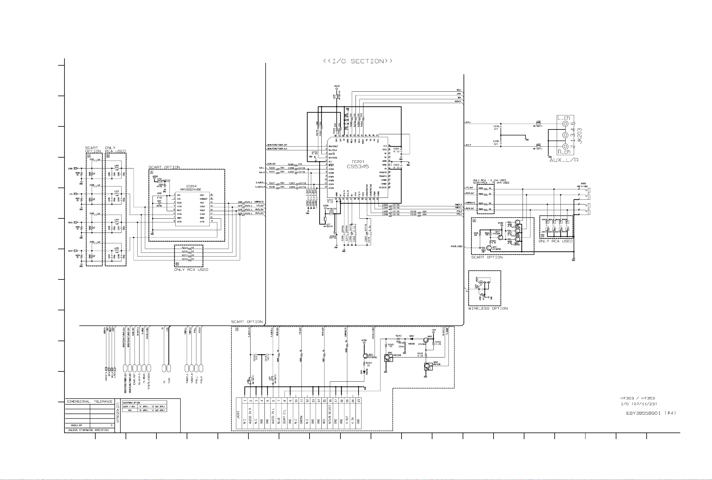
5. I/O CIRCUIT DIAGRAM
2007. 11. 30
A
1
2
3
4
5
6
7
8
9
10
11
12
B C D E F G H I J K L M N O P Q R ST
Page 61

Copyright © 2008 LG Electronics. Inc. All right reserved.
Only for training and service purposes
LGE Internal Use Only
2-59 2-60
6. AMP CIRCUIT DIAGRAM
2007. 11. 30
A
1
2
3
4
5
6
7
8
9
10
11
12
B C D E F G H I J K L M N O P Q R ST
Page 62

Copyright © 2008 LG Electronics. Inc. All right reserved.
Only for training and service purposes
LGE Internal Use Only
2-61 2-62
7. MIC CIRCUIT DIAGRAM
2007. 11. 30
A
1
2
3
4
5
6
7
8
9
10
11
12
B C D E F G H I J K L M N O P Q R ST
Page 63

Copyright © 2008 LG Electronics. Inc. All right reserved.
Only for training and service purposes
LGE Internal Use Only
2-63 2-64
8. FRONT CIRCUIT DIAGRAM
2007. 11. 30
A
1
2
3
4
5
6
7
8
9
10
11
12
B C D E F G H I J K L M N O P Q R ST
Page 64

2-65 2-66
9. PWR KEY CIRCUIT DIAGRAM
Copyright © 2008 LG Electronics. Inc. All right reserved.
Only for training and service purposes
LGE Internal Use Only
2007. 11. 30
A
1
2
3
4
5
6
7
8
9
10
11
12
B C D E F G H I J K L M N O P Q R ST
Page 65

2-67 2-68
10. MIC & USB & PTB CIRCUIT DIAGRAM
2007. 11. 30
A
1
2
3
4
5
6
7
8
9
10
11
12
B C D E F G H I J K L M N O P Q R ST
Copyright © 2008 LG Electronics. Inc. All right reserved.
Only for training and service purposes
LGE Internal Use Only
Page 66

Copyright © 2008 LG Electronics. Inc. All right reserved.
Only for training and service purposes
LGE Internal Use Only
2-69 2-70
PRINTED CIRCUIT BOARD DIAGRAMS
1. MAIN P.C. BOARD DIAGRAM ( TOP VIEW )
Page 67

Copyright © 2008 LG Electronics. Inc. All right reserved.
Only for training and service purposes
LGE Internal Use Only
2-71 2-72
MAIN P.C. BOARD DIAGRAM ( BOTTOM VIEW )
Page 68

Copyright © 2008 LG Electronics. Inc. All right reserved.
Only for training and service purposes
LGE Internal Use Only
2-73 2-74
2. SMPS P.C. BOARD DIAGRAM
NOTE: Warning
Parts that are shaded are critical With
respect to risk of fire or electrical shock.
Page 69

Copyright © 2008 LG Electronics. Inc. All right reserved.
Only for training and service purposes
LGE Internal Use Only
TIMER P.C BOARD DIAGRAM (HT353)
2-75 2-76
3. TIMER P.C BOARD DIAGRAM (HT303)
4. KEY P.C. BOARD DIAGRAM (HT303) KEY P.C. BOARD DIAGRAM (HT353)
5. FRONT JACK P.C. BOARD DIAGRAM
Page 70

3-1 3-2
Copyright © 2008 LG Electronics. Inc. All right reserved.
Only for training and service purposes
LGE Internal Use Only
• CABINET AND MAIN FRAME SECTION
SECTION 3. EXPLODED VIEWS
A50
452
A43
PN302
283
A26
C
CABLE1
463
A47
463
NOTES) THE EXCLAMATION POINT WITHIN AN
462
A
B
A
B
250
EQUILATERAL TRIANGLE IS INTENDED
TO ALERT THE SERVICE PERSONNEL
TO THE PRESENCE OF IMPORTANT
SAFETY INFORMATION IN SERVICE
LITERATURE.
463
462
279
A41
D
PN202
FRONT JACK
467
262
275
275
SMPS
261
MAIN
E
CD
465
A46
300
465
E
A44
260
261
Page 71

3-3 3-4
Copyright © 2008 LG Electronics. Inc. All right reserved.
Only for training and service purposes
LGE Internal Use Only
• DECK MECHANISM EXPLODED VIEW(DP-12TV)
A26
001
A02
017
013
435
015
439
018
015B
015A
014
440
002
003
A01
020
016
026
A03
019
442
012
010
012
012A
442
Page 72

3-5
Copyright © 2008 LG Electronics. Inc. All right reserved.
Only for training and service purposes
LGE Internal Use Only
• PACKING ACCESSORY SECTION
BATTERY
808
OWNER'S MANUAL
801
REMOTE CONTROL
900
BAG
804
PACKING, CASING
803
BOX
802
PACKING, CASING
803
825
FM WIRE ANTENNA
OPTIONAL PART
818
PORTABLE IN CABLE
Page 73

3-6
Copyright © 2008 LG Electronics. Inc. All right reserved.
Only for training and service purposes
LGE Internal Use Only
1. SATELLITE SPEAKER(SH33SU-S)
• SPEAKER SECTION
A80
F.L SPK
F.R SPK
A81
CENTER SPK
A82
A83
R.L SPK
R.R SPK
A84
853
850
851
852
WIRE80
WIRE81
WIRE82
WIRE83
WIRE84
F.L SPK
F.R SPK
CENTER SPK
R.L SPK
R.R SPK
Page 74

3-7
Copyright © 2008 LG Electronics. Inc. All right reserved.
Only for training and service purposes
LGE Internal Use Only
2. SATELLITE SPEAKER(SH33SD-S)
A80
F.L SPK
F.R SPK
A81
CENTER SPK
A82
A83
R.L SPK
R.R SPK
A84
853
850
851
852
WIRE80
WIRE81
WIRE82
WIRE83
WIRE84
F.L SPK
F.R SPK
CENTER SPK
R.L SPK
R.R SPK
Page 75

3-8
Copyright © 2008 LG Electronics. Inc. All right reserved.
Only for training and service purposes
LGE Internal Use Only
3. PASSIVE SUBWOOFER(SH33SU-W/SH33SD-W)
950
A90
951
952
WIRE90
956
954
955
953
Page 76

4-1
Copyright © 2008 LG Electronics. Inc. All right reserved.
Only for training and service purposes
LGE Internal Use Only
SECTION 4.
MECHANISM (DP-12TV)
[CONTENTS]
DECK MECHANISM PARTS LOCATIONS
• Top View . . . . . . . . . . . . . . . . . . . . . . . . . . . . . . . . . . . . . . . . . . . . . . . . . . . . . . . . . . . . 4-2
• Top View(without Tray Disc) . . . . . . . . . . . . . . . . . . . . . . . . . . . . . . . . . . . . . . . . . . . . . 4-2
• Bottom View . . . . . . . . . . . . . . . . . . . . . . . . . . . . . . . . . . . . . . . . . . . . . . . . . . . . . . . . . 4-2
DECK MECHANISM DISASSEMBLY
1. Main Base . . . . . . . . . . . . . . . . . . . . . . . . . . . . . . . . . . . . . . . . . . . . . . . . . . . . . . . . . . 4-3
1-1. Clamp Assembly Disc . . . . . . . . . . . . . . . . . . . . . . . . . . . . . . . . . . . . . . . . . . . . . . 4-3
1-1-1. Plate Clamp . . . . . . . . . . . . . . . . . . . . . . . . . . . . . . . . . . . . . . . . . . . . . . . . . 4-3
1-1-2. Magnet Clamp . . . . . . . . . . . . . . . . . . . . . . . . . . . . . . . . . . . . . . . . . . . . . . . 4-3
1-1-3. Clamp Upper . . . . . . . . . . . . . . . . . . . . . . . . . . . . . . . . . . . . . . . . . . . . . . . . 4-3
2. Tray Disc . . . . . . . . . . . . . . . . . . . . . . . . . . . . . . . . . . . . . . . . . . . . . . . . . . . . . . . . . . . 4-3
3. Base Assembly Sled . . . . . . . . . . . . . . . . . . . . . . . . . . . . . . . . . . . . . . . . . . . . . . . . . 4-4
3-1. Gear Feed . . . . . . . . . . . . . . . . . . . . . . . . . . . . . . . . . . . . . . . . . . . . . . . . . . . . . . . 4-4
3-2. Gear Middle . . . . . . . . . . . . . . . . . . . . . . . . . . . . . . . . . . . . . . . . . . . . . . . . . . . . . . 4-4
3-3. Gear Rack . . . . . . . . . . . . . . . . . . . . . . . . . . . . . . . . . . . . . . . . . . . . . . . . . . . . . . . 4-4
4. Rubber Rear . . . . . . . . . . . . . . . . . . . . . . . . . . . . . . . . . . . . . . . . . . . . . . . . . . . . . . . . 4-4
5. Frame Assembly Up/Down . . . . . . . . . . . . . . . . . . . . . . . . . . . . . . . . . . . . . . . . . . . . . 4-5
6. Belt Loading . . . . . . . . . . . . . . . . . . . . . . . . . . . . . . . . . . . . . . . . . . . . . . . . . . . . . . . . 4-5
7. Gear Pulley . . . . . . . . . . . . . . . . . . . . . . . . . . . . . . . . . . . . . . . . . . . . . . . . . . . . . . . . . 4-5
8. Gear Loading . . . . . . . . . . . . . . . . . . . . . . . . . . . . . . . . . . . . . . . . . . . . . . . . . . . . . . . 4-5
9. Guide Up/Down . . . . . . . . . . . . . . . . . . . . . . . . . . . . . . . . . . . . . . . . . . . . . . . . . . . . . 4-5
10. PWB Assembly Loading . . . . . . . . . . . . . . . . . . . . . . . . . . . . . . . . . . . . . . . . . . . . . 4-5
11. Base Main . . . . . . . . . . . . . . . . . . . . . . . . . . . . . . . . . . . . . . . . . . . . . . . . . . . . . . . . . 4-5
EXPLODED VIEW
1. DECK MECHANISM EXPLODED VIEW (DP-12TV) . . . . . . . . . . . . . . . . . . . . . . . . . . . 4-6
Page 77

4-2
Copyright © 2008 LG Electronics. Inc. All right reserved.
Only for training and service purposes
LGE Internal Use Only
DECK MECHANISM PARTS LOCATIONS
Starting No.
1
1, 2
1, 2, 3
1, 2, 3, 4
1
1, 6
1, 2, 6
1, 2, 6, 8
1, 2, 6, 8,
9
1, 2, 7
1, 2, 7
1, 2
1, 2 ,13
1, 2, 13, 14
1, 2, 7, 12, 13,
14
1, 2, 13
1, 2, 7, 12, 13,
14, 15, 16, 17
1
2
3
4
5
6
7
8
9
10
11
12
13
14
15
16
17
18
Main Base
Clamp Assembly
Disc
Plate Clamp
Magnet Clamp
Clamp Upper
Tray Disc
Base Assembly Sled
Gear Feed
Gear
Middle
Gear Rack
Rubber Rear
Frame Assembly
Up/Down
Belt Loading
Gear Pulley
Gear Loading
Guide Up/Down
PWB Assembly
Loading
Base Main
4 Screws,
1 Connector
1 Locking Tabs
1 Screw
1 Screw
1 Locking Tab
1 Locking Tab
1 Locking Tab
1 Hook
2Screw
2 Locking Tabs
4-1
4-1
4-1
4-1
4-1
4-2
4-3
4-3
4-3
4-3
4-3
4-4
4-4
4-4
4-4
4-4
4-4
4-4
Bottom
Bottom
Procedure
Parts Fixing Type
Figure
Disass
embly
Note
When reassembling, perform the procedure in
reverse order.
The “Bottom” on Disassembly column of above
Table indicates the part should be disassembled
at the Bottom side.
• Top View(without Tray Disc)
• Bottom View
• Top View
Page 78
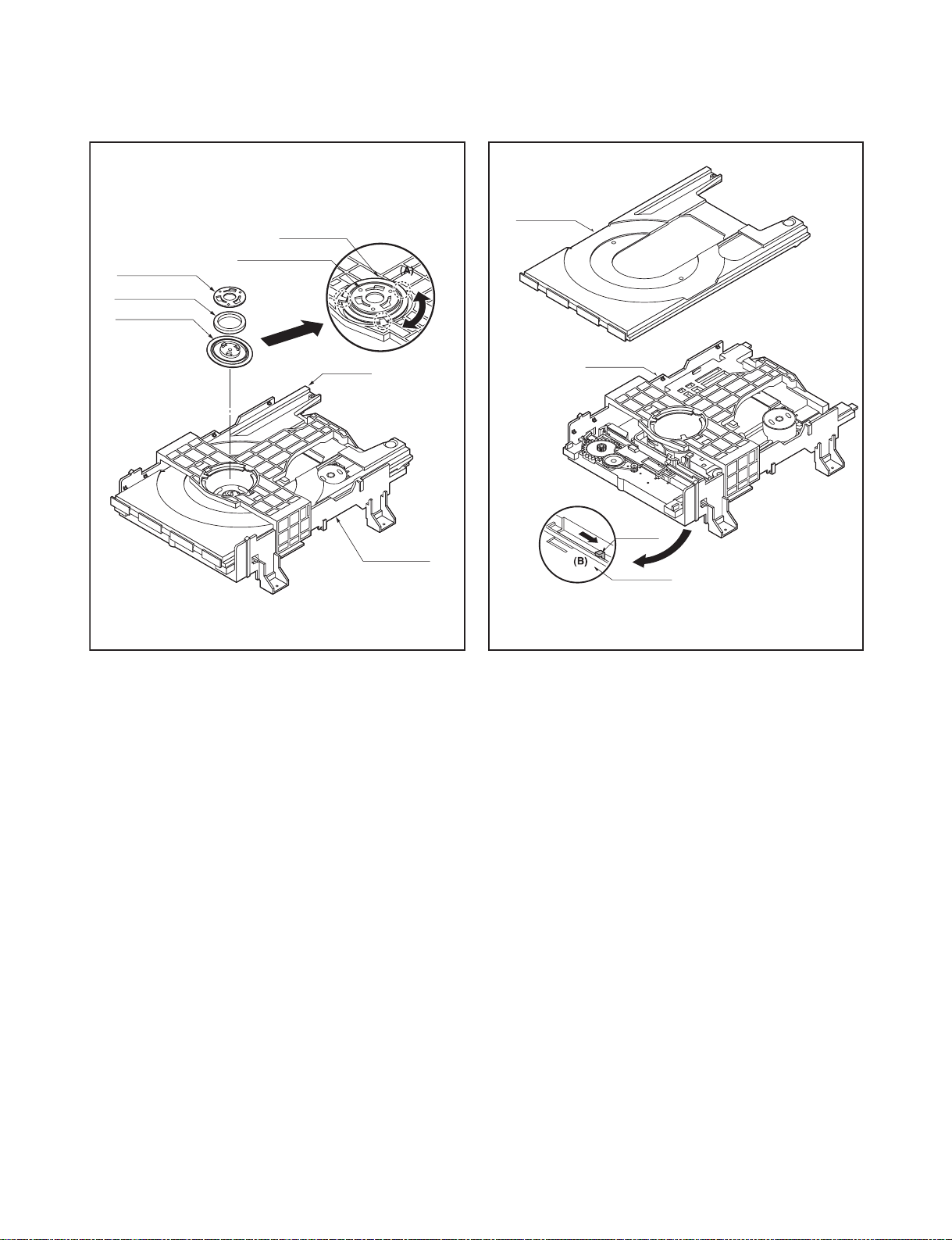
4-3
Copyright © 2008 LG Electronics. Inc. All right reserved.
Only for training and service purposes
LGE Internal Use Only
DECK MECHANISM DISASSEMBLY
1. Main Base (Fig. 4-1)
1-1. Clamp Assembly Disc
1) Place the Clamp Assembly Disc as Fig. (A)
2) Lift up the Clamp Assembly Disc in direction of
arrow(A).
3) Separate the Clamp Assembly Disc from the
Holder Clamp.
1-1-1. Plate Clamp
1) Turn the Plate Clamp to counterclockwise
direction and then lift up the Plate Clamp.
1-1-2. Magnet Clamp
1-1-3. Clamp Upper
2. Tray Disc (Fig. 4-2)
1) Insert and push a Driver in the emergency eject
hole(A) at the right side, or put the Driver on the
Lever(B) of the Gear Emergency and pull the
Lever(B) in direction of arrow so that the Tray Disc
is ejected about 15~20mm.
2) Pull the Tray Disc until it is separated from the
Base Main completely.
PLATE CLAMP
MAGNET CLAMP
CLAMP UPPER
TRAY DISC
MAIN BASE
DISC CLAMP ASSEMBLY
HOLDER
(Fig. A)
BASE MAIN
BASE MAIN
LEVER
BASE MAIN
BOTTOM SIDE VIEW
Fig. 4-2Fig. 4-1
Page 79

4-4
Copyright © 2008 LG Electronics. Inc. All right reserved.
Only for training and service purposes
LGE Internal Use Only
3. Base Assembly Sled (Fig. 4-3)
1) Release 4 Screw(S2).
2) Disconnect the FFC Connector(C1)
3-1. Gear Feed
3-2. Gear Middle
3-3. Gear Rack
1) Release the Scerw(S3)
4. Rubber Rear (Fig. 4-3)
RUBBER DAMPER
RUBBER DAMPER
Distinguish upper and
lower sides
(Assemble with care)
RUBBER DAMPER
Distinguish upper and
lower sides
(Assemble with care)
BASE PU
GENERAL PICK UP ASSEMBLY
GEAR RACK
SPINDLE MOTOR ASSEMBLY
(S2)
(S2)
RUBBER DAMPER
Fig. 4-3
Page 80

4-5
Copyright © 2008 LG Electronics. Inc. All right reserved.
Only for training and service purposes
LGE Internal Use Only
5. Frame Assembly Up/Down (Fig. 4-4)
Note
Put the Base Main face down(Bottom Side)
1) Release the screw(S4)
2) Unlock the Locking Tab(L3) in direction of arrow
and then lift up the Frame Assembly Up/Down to
separate it from the Base Main.
Note
• When reassembling move the Guide Up/Down in
direction of arrow(C) until it is positioned as
Fig.(C).
• When reassembling insert (A) portion of the Frame
Assembly Up/Down in the (B) portion of the Guide
Up/Down as Fig.(B)
6. Belt Loading(Fig. 4-4)
Note
Put the Base Main on original position(Top Side)
7. Gear pulley (Fig. 4-4)
1) Unlock the Locking Tab(L4) in direction of arrow(B) and
then separate the Gear Pulley from the Base Main.
8. Gear Loading (Fig. 4-4)
9. Guide Up/Down (Fig. 4-4)
1) Move the Guide Up/Down in direction of arrow(A) as
Fig.(A)
2) Push the Locking Tab(L5) down and then lift up the
Guide Up/Down to separate it from the Base Main.
Note
When reassembling place the Guide Up/Down as Fig.(C)
and move it in direction arrow(B) until it is locked by the
Locking Tab(L5). And confirm the Guide Up/Down as Fig.(A)
10. PWB Assembly Loading (Fig. 4-4)
Note
Put the Base Main face down(Bottom Side)
1) Release 1 Screws(S5)
2) Unlock the Loading Motor (C2) from the Hook (H1) on
the Base Main.
3) Unlock 2 Locking Tabs(L6) and separate the PWB
Assembly Loading from the Base Main.
11. Base Main(Fig. 4-4)
GEAR LOADING
GUIDE UP/DOWN
SCREW INSERTION
TORGUE CONTROL
(800gf DOWN)
GUIDE UP/DOWN
GEAR PULLEY
(L4)
BELT LOADING
(A)
(L5)
FIG. (A)
PWB ASSEMBLY LOADING
BASE MAIN
(B)
(C)
(B)
FIG. (C)
(S5)
(A)
GUIDE UP/DOWN
Fig. 4-4
(H1)
(C2)
(A)
(B)
FIG. (B)
GUIDE UP/DOWN
(L6)
(L6)
BASE MAIN
(S4)
(S4)
UP/DOWN FRAME ASSEMBLY
Page 81

4-6
Copyright © 2008 LG Electronics. Inc. All right reserved.
Only for training and service purposes
LGE Internal Use Only
DECK MECHANISM EXPLODED VIEW (DP-12TV)
A26
001
A02
017
013
435
015
439
018
015B
015A
014
440
002
003
A01
020
016
026
A03
019
442
012
010
012A
012
442
 Loading...