

Page 1

PLASMA TV
SERVICE MANUAL
CAUTION
BEFORE SERVICING THE CHASSIS,
READ THE SAFETY PRECAUTIONS IN THIS MANUAL.
CHASSIS : RF-043B
MODEL : RZ-60PY10
website:http://biz.LGservice.com
e-mail:http://www.LGEservice.com/techsup.html
Page 2

- 2 -
CONTENTS
SAFETY PRECAUTIONS ...................................................................................3
DESCRIPTION OF CONTROLS .........................................................................4
SPECIFICATIONS .............................................................................................14
ADJUSTMENT INSTRUCTIONS ......................................................................16
TROUBLE SHOOTING GUIDE..........................................................................21
BLOCK DIAGRAM.............................................................................................32
EXPLODED VIEW..............................................................................................34
EXPLODED VIEW PARTS LIST........................................................................35
REPLACEMENT PARTS LIST...........................................................................36
SCHEMATIC DIAGRAM ........................................................................................
PRINTED CIRCUIT BOARD ..................................................................................
Page 3
- 3 -
SAFETY PRECAUTIONS
Many electrical and mechanical parts in this chassis have special safety-related characteristics. These parts are identified by in
the Schematic Diagram and Replacement Parts List.
It is essential that these special safety parts should be replaced with the same components as recommended in this manual to
prevent X-RADIATION, Shock, Fire, or other Hazards.
Do not modify the original design without permission of manufacturer.
General Guidance
An isolation Transformer should always be used during
the servicing of a receiver whose chassis is not isolated from
the AC power line. Use a transformer of adequate power rating
as this protects the technician from accidents resulting in
personal injury from electrical shocks.
It will also protect the receiver and it's components from being
damaged by accidental shorts of the circuitry that may be
inadvertently introduced during the service operation.
If any fuse (or Fusible Resistor) in this monitor is blown, replace
it with the specified.
When replacing a high wattage resistor (Oxide Metal Film
Resistor, over 1W), keep the resistor 10mm away from PCB.
Keep wires away from high voltage or high temperature parts.
Due to high vacuum and large surface area of picture tube,
extreme care should be used in handling the Picture Tube.
Do not lift the Picture tube by it's Neck.
Leakage Current Cold Check(Antenna Cold Check)
With the instrument AC plug removed from AC source,
connect an electrical jumper across the two AC plug prongs.
Place the AC switch in the on position, connect one lead of
ohm-meter to the AC plug prongs tied together and touch other
ohm-meter lead in turn to each exposed metallic parts such as
antenna terminals, phone jacks, etc.
If the exposed metallic part has a return path to the chassis, the
measured resistance should be between 1MΩ and 5.2MΩ.
When the exposed metal has no return path to the chassis the
reading must be infinite.
An other abnormality exists that must be corrected before the
receiver is returned to the customer.
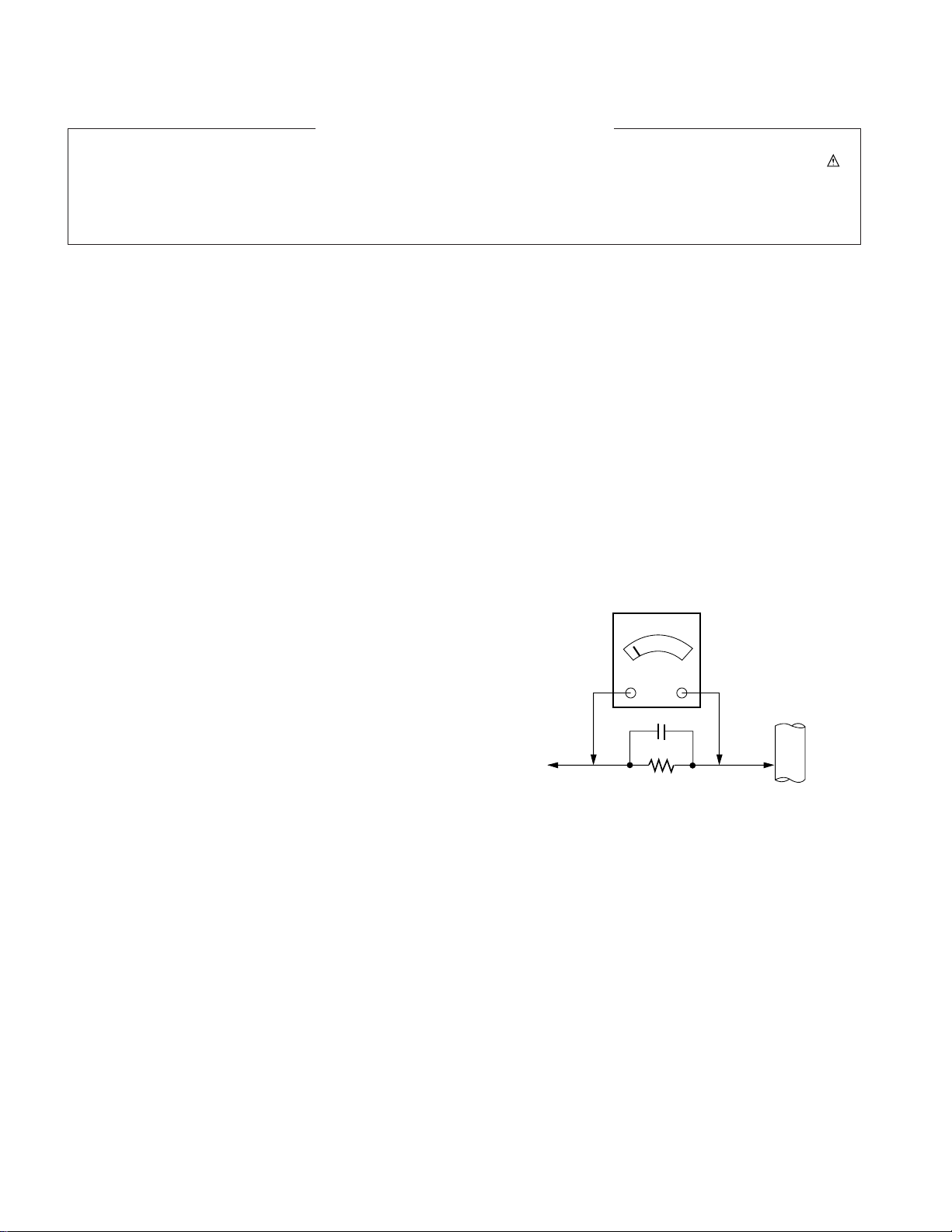
Leakage Current Hot Check (See below Figure)
Plug the AC cord directly into the AC outlet.
Do not use a line Isolation Transformer during this check.
Connect 1.5K/10watt resistor in parallel with a 0.15uF capacitor
between a known good earth ground (Water Pipe, Conduit, etc.)
and the exposed metallic parts.
Measure the AC voltage across the resistor using AC
voltmeter with 1000 ohms/volt or more sensitivity.
Reverse plug the AC cord into the AC outlet and repeat AC
voltage measurements for each exposed metallic part. Any
voltage measured must not exceed 0.75 volt RMS which is
corresponds to 0.5mA.
In case any measurement is out of the limits specified, there is
possibility of shock hazard and the set must be checked and
repaired before it is returned to the customer.
Leakage Current Hot Check circuit
1.5 Kohm/10W
To Instrument's
exposed
METALLIC PARTS
Good Earth Ground
such as WATER PIPE,
CONDUIT etc.
AC Volt-meter
IMPORTANT SAFETY NOTICE
0.15uF
Page 4
- 4 -
DESCRIPTION OF CONTROLS
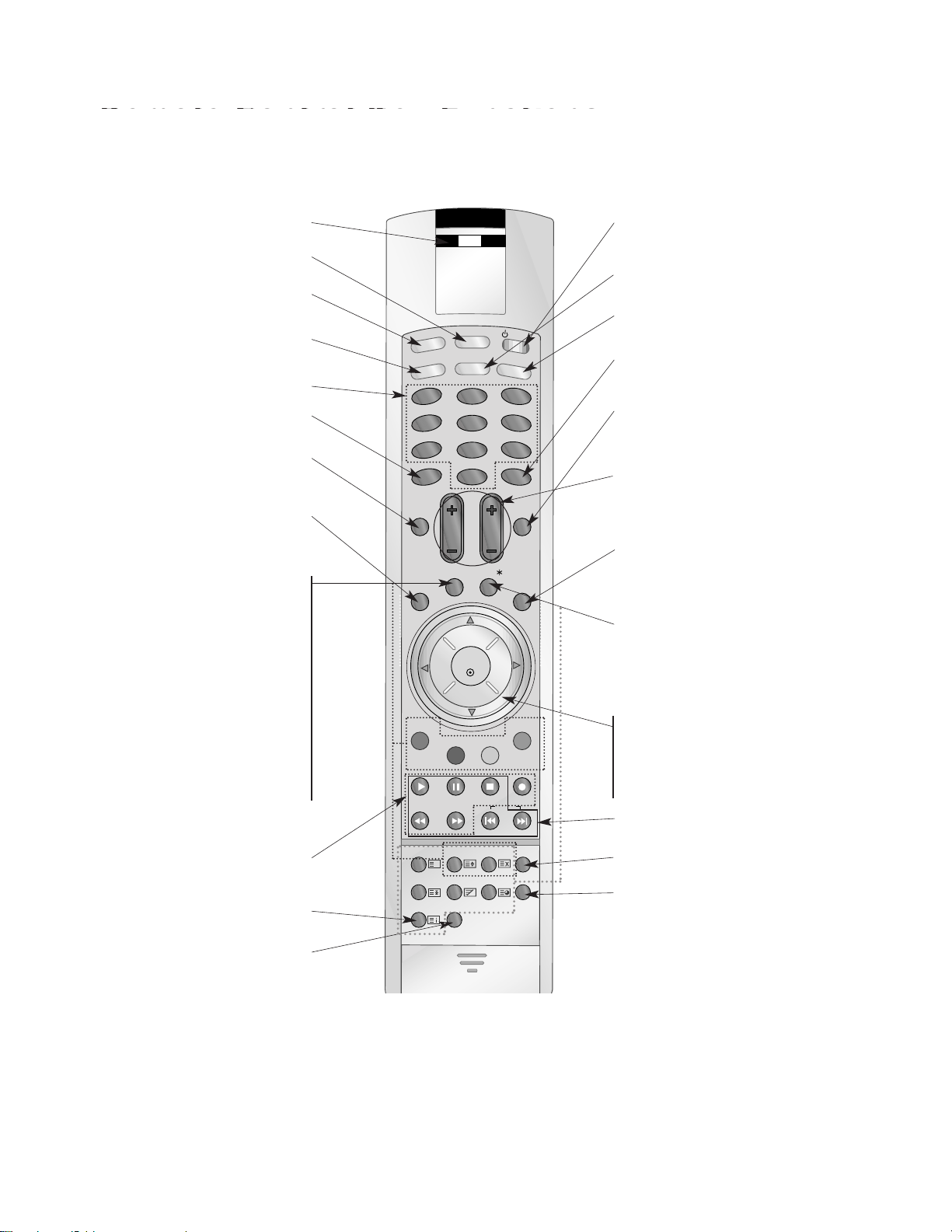
Remote Control Key Functions
Remote Control Key Functions
- When using the remote control aim it at the remote control sensor of the set.
- There's maybe a defect in consecutive operation of remote control in specified brightness according to this set feature.
123
456
789
0
DVD
STB
AUDIO
MODE
POWER
MUTE
TV/AV
MULTIMEDIA
ARC
SSM
Q.VIEW
PSM
FAVOURITE
MENU
PIP PR-
REVEAL
LIST
PLAY
REW FF SKIP
PAUSE STOP
RECORD
SPLIT ZOOM
SLEEP
I/II
WIN.SIZE
WIN.POSITION
PIP INPUT
PIP PR+ SWAP
OK
PIP/DW
EXIT
PR
VOL
CABLE
VCR
?
TV
TEXT/
Displays the selected device.
TV/AV
Selects the TV, AV, Component, RGB
or DVI modes.
MODE
Selects another device.
NUMBER buttons
PIP/DW
Switches the sub picture on or off.
Selects PIP or DW modes.
PIP PR + /-
Selects a program for the sub picture.
SWAP
Alternates between main and sub pic-
ture.
PIP INPUT
Selects the input mode for the sub pic-
ture.
WIN.SIZE
Adjusts the sub picture size.
WIN.POSITION
Moves the sub picture to
DD/ EE
or FF/
GG
direction.
OK
accepts your selection or displays the
current mode.
DD/ EE
or FF/
GG
Adjusts menu settings.
Selects menu item.
POWER
Switches the set on from standby or
off to standby.
ARC
Changes the picture format.
MUTE
Switches the sound on or off.
Q.VIEW
Returns to the previously viewed
programme.
SSM
To select the sound appropriate to
your viewing programme character.
VOL +/- (Volume Up/Down)
Increases/decreases sound level.
PR +/- (Programme Up/Down)
Selects a programme.
EXIT
Clears all on-screen displays and
returns to TV viewing from any
menu.
DVD BUTTONS
Controls a LG DVD player.
SLEEP
Sets the sleep timer.
I/II
Selects the language during dual language broadcast.
Selects the sound output.
TEXT/*(option)
These buttons are used for teletext.
For further details, see the ‘Teletext’
section.
Note : In teletext mode, the PIP PR
+/-, SWAP and PIP INPUT buttons are
used for teletext function.
MULTIMEDIA
Selects the Component, RGB or DVI
modes.
FAVOURITE
Selects a favorite programme.
PSM
Adjusts the factory preset picture
according to the room.
MENU
Displays on screen menus one by one.
Exits the current menu.
Memorizes menu changes.
VCR BUTTONS
Controls a LG video cassette
recorder.
LIST
Displays the program table.
SPLIT ZOOM
Enlarge the screen with regular
ration.
Page 5
- 5 -
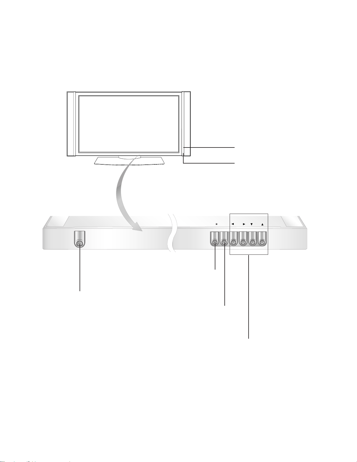
<Front Panel Controls>
TV/AVON/OFF MENU VOL PR
- Shown is a simplified representation of the set.
- Here shown may be somewhat different from your set.
Main Power Button
Remote Control Sensor
TV/AV Button
Selects the TV, AV, Component,
RGB or DVI modes. If OSD is dis-
played, selects menu item.
MENU
Displays on screen menus one by one.
Exits the current menu.
Memorizes menu changes.
DD/ EE
(Programme Up/Down)
selects a programme or a menu item.
switches the set on from standby.
FF/ GG
(Volume Up/Down)
adjusts the volume.
adjusts menu settings.
Power Standby Indicator
Illuminates red in standby
mode, Illuminates green
when the set is turned on
Page 6
- 6 -
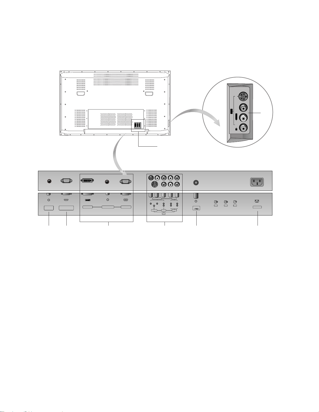
Antenna
REMOTE
CONTROL
RS-232C INPUT DVI INPUT
(CONTROL/SERVICE)
AC INPUT
AUDIO INPUT RGB INPUT
Y P
B PR L R
L
(MONO)
R
COMPONENT
S-VIDEO VIDEO AUDIO
AUDIO
AV4
AV1 AV2 AV3
<Back Panel>
1. REMOTE CONTROL
2. RS-232C INPUT(CONTROL/SERVICE) PORT
Connect to the RS-232C port on a PC.
3. DVI INPUT / AUDIO INPUT / RGB INPUT
Connect the monitor output socket of the PERSONAL COMPUTER to this socket.
Note: If you want to use RGB/DVI audio, we strongly recommend that you use the cable that has a core, or the EMI Fillter
core along with separete cable.
4. COMPONENT INPUT
Connect DVD video outputs to Y, PB, PR of COMPONENT
INPUT and audio outputs to Audio sockets of AUDIO INPUT.
AUDIO/VIDEO IN SOCKETS (AV4)
Connect the audio/video out sockets of external equipment to
these sockets.
S-VIDEO/AUDIO IN SOCKETS
Connect the S-VIDEO out socket of an VCR to the S-VIDEO
socket.
Connect the audio out sockets of the VCR to the audio sockets as in AV4.
5. ANTENNA INPUT
6. EURO SCART SOCKET
Connect the euro scart socket of the VCR to these sockets.
7. POWER CORD SOCKET
This Monitor operates on an AC power. The voltage is indicated on the Specifications page. Never attempt to operate
the Monitor on DC power.
8. AUDIO/VIDEO IN SOCKETS (AV5)
S-VIDEO/AUDIO IN SOCKETS
6
8
S-VIDEOVIDEOAUDIO
AV 5
R
L/MONO
3 4 751 2
Page 7
- 7 -
External Equipment V
External Equipment V
iewing Setups
iewing Setups
- Be careful for the bronze wire not to be bended in connecting to antenna input port.
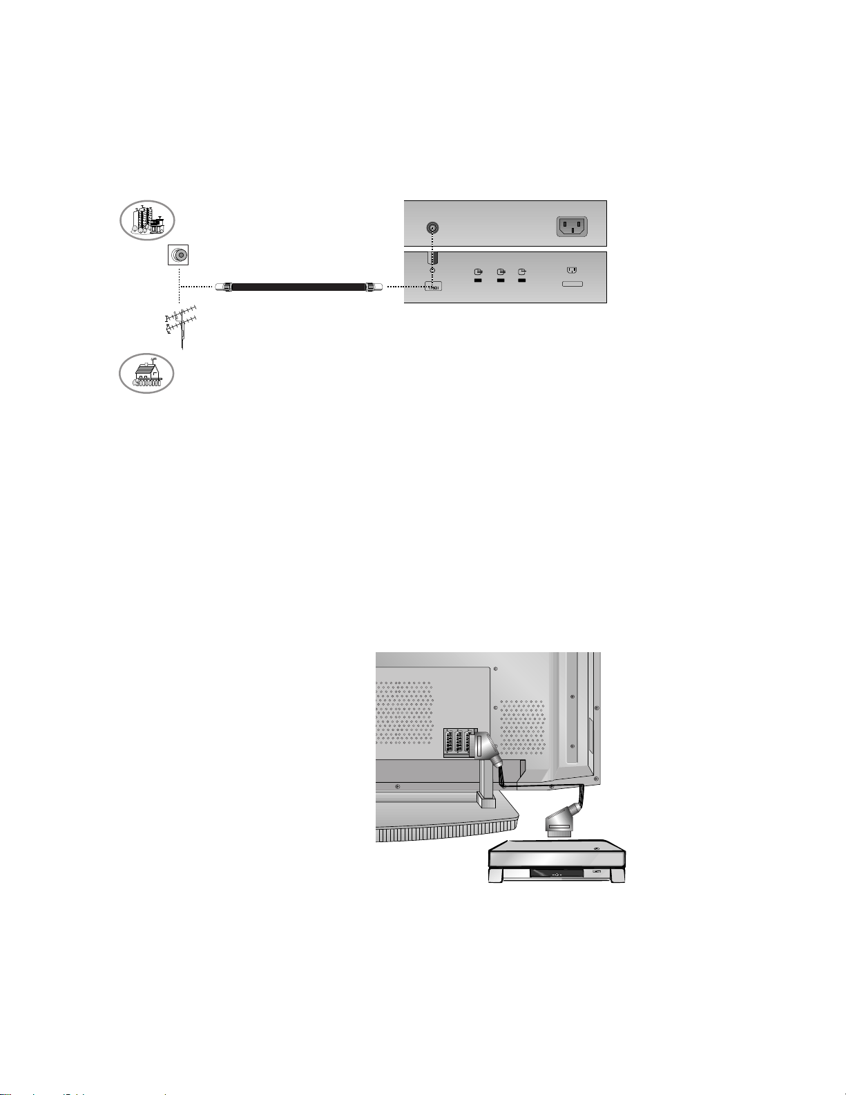
Antenna Connection
Antenna
OL
RS-232C INPUT DVI INPUT
(CONTROL/SERVICE)
AC INPUT
AUDIO INPUT RGB INPUT
Y P
B PR L R
L
(MONO)
R
COMPONENT
S-VIDEO VIDEO AUDIO
AUDIO
AV4
AV1 AV2 AV3
Watching VCR
- When connecting the set to external equipment, match the colours of connecting ports (Video - yellow, Audio (L) - white, Audio
(R) -red).
- Connect the VIDEO INPUT socket (yellow) to the VIDEO INPUT on the set.
- If you have a mono VCR, connect the audio cable from the VCR to the AUDIO (L/MONO) input on the set.
- If you connect an S-VIDEO VCR to the S-VIDEO input, the picture quality is improved; compared to connecting a regular VCR
to the Video input.
Or, connect the Euro scart socket of the VCR to the Euro scart socket of the set.
- Use the orbiter function to Avoid having a fixed image remain on the screen for a long period of time. Typically a frozen still picture from a VCR. (Refer to p. 25)
If a 4:3 picture format is used; the fixed image may remain visible on the screen.
- To avoid picture noise (interference), leave an adequate distance between the VCR and set.
Watching TV programmes
- Turn the set on and select the programme you
want.
Watching VCR
1. Use the TV/AV button on the remote control to
select
AV1, AV2, AV3, AV4 or AV5.
- If both S-VIDEO and VIDEO sockets have been
connected to the S-VHS VCR simultaneously, only
the S-VIDEO can be received.
2. Insert a video tape into the VCR and press the
PLAY button on the VCR.
(See VCR owner’s manual)
Apartments
(connecting to wall antenna socket)
Private house
(connecting to wall outdoor antenna)
outdoor antenna
wall antenna socket
VHF antenna
UHF antenna
RF coaxial wire (75 ohms)
< Back panel of the set >
< Back panel of the set >
< VCR >
Page 8
- 8 -
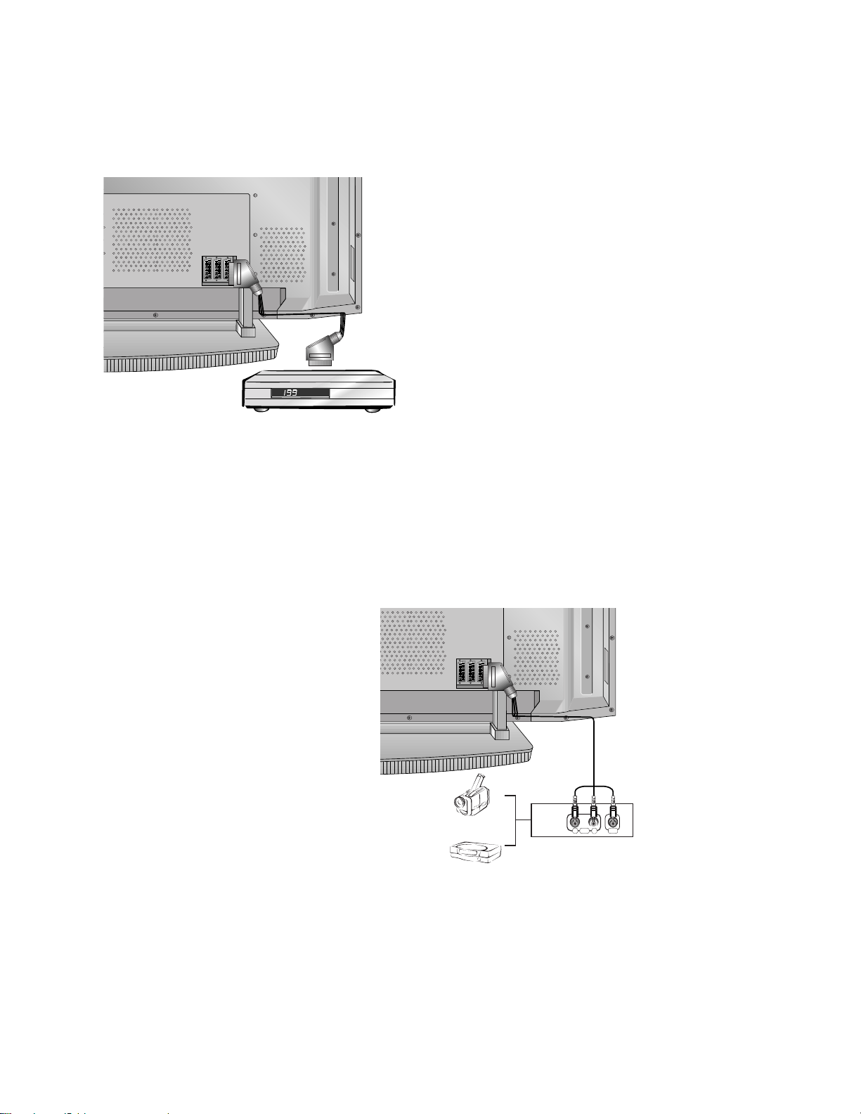
Watching Cable TV
- After subscribing for a local cable TV station and installing a converter you can watch cable TV.
- For further information of cable TV, contact the local cable TV station.
To watch cable TV
1. Use the TV/AV button on the remote control to
select
AV1, AV2, AV3, AV4 or AV5.
2. Tune to cable service provided channels using
the cable box.
Watching external AV source
- When connecting the set to an external source, match the colours of AUDIO/VIDEO input jacks on the set with the output jacks
on the audio/video equipment: Video = yellow, Audio (Left) = white, Audio (Right) = red.
Or, connect the Euro scart socket of the VCR to the Euro scart socket of the set.
How to use
1. Use the TV/AV button on the remote control to
select
AV1, AV2, AV3, AV4 or AV5.
2. Operate the corresponding external equipment.
See external equipment operating guide.
R L
AUDIO VIDEO
R
< Back panel of the set >
< Cable box >
< Back panel of the set >
Camcorder
Video game set
Page 9
- 9 -
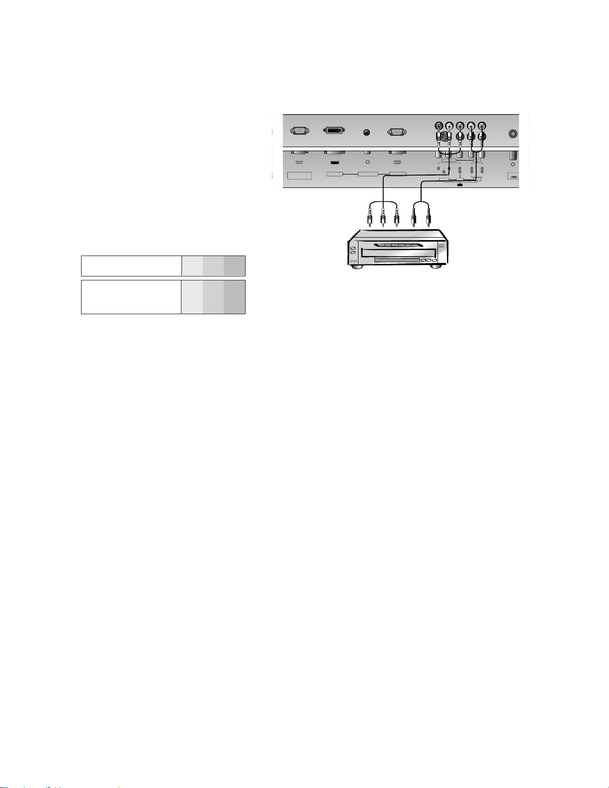
Watching DVD
How to connect
Connect DVD video outputs to Y, PB, PR of COMPONENT INPUT and audio outputs to Audio sockets of
AUDIO INPUT.
How to use
1. Turn on the DVD player, and insert a DVD.
2. Use TV/AV or MULTIMEDIA button on the remote
control to select
Component. Refer to the DVD player's
manual for operating instructions.
• Component Input ports
You can get better picture quality if you connect
DVD player with component input ports as below.
Component ports of the
set
Y
PB
PR
Video output ports
of DVD player
Y
Y
Y
Y
Pb
B-Y
Cb
PB
Pr
R-Y
Cr
P
R
Antenna
ROL
RS-232C INPUT DVI INPUT
(CONTROL/SERVICE)
AUDIO INPUT RGB INPUT
Y P
B PR L R
L
(MONO)
R
COMPONENT
S-VIDEO VIDEO AUDIO
AUDIO
AV4
R
R
R
R
< Back panel of the set >
< DVD player >
Page 10
- 10 -
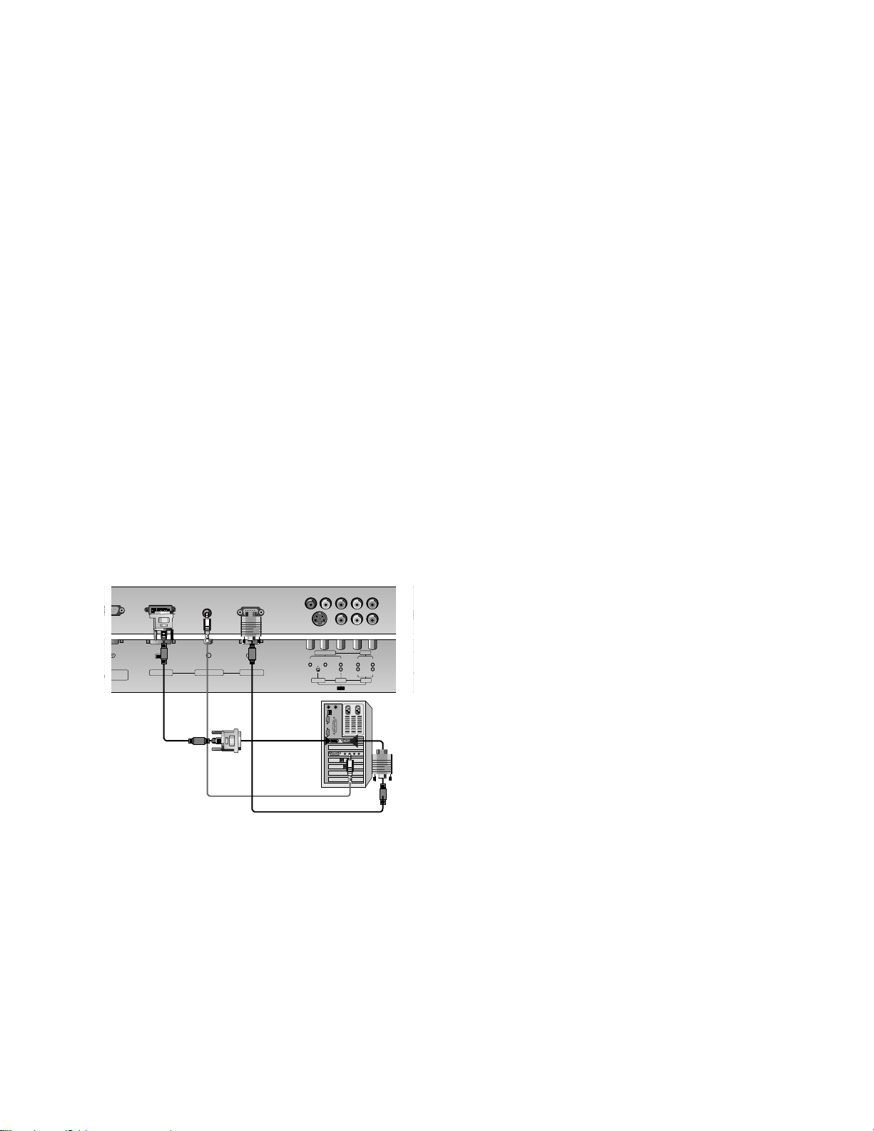
Connecting PC
- To enjoy vivid picture and sound, connect a PC to the set.
- Avoid keeping a fixed image on the set’s screen for a long period of time. The fixed image may become permanently imprinted on
the screen; use a screen saver when possible.
- Connect PC to the RGB INPUT(PC INPUT) or DVI INPUT(DIGITALRGB INPUT) port of the set; change the resolution output of
PC accordingly.
- There might be a noise according to some resolution, vertical pattern, contrast or brightness in PC mode. Then change the PC
mode into other resolution or change the refresh rate into other rate or adjust the brightness and contrast on the menu until the
picture is clean. If the refresh rate of the PC graphic card can not be changed, change the PC graphic card or consult it to the
manufacturer of the PC graphic card.
- The synchronization input form for Horizontal and Vertical frequencies is separate.
Setup Instructions to Connect a PC to your set
- We recommend using 1024x768, 60Hz for the PC mode, they provide the best picture quality.
- If the resolution of PC is over UXGA, there will be no picture on the set.
- Connect the signal cable from the monitor output port of the PC to the RGB INPUT port of the set or the signal cable from the DVI
output port of the PC to the DVI INPUT port on the set.
- Connect the audio cable from the PC to the Audio input on the set. (Audio cables are not included with the set).
- If using a sound card, adjust PC sound as required.
- This set apply a VESAPlug and Play Solution. The set provides EDID data to the PC system with a DDC protocol. The PC adjusts
automatically to use this set.
- DDC protocol is preset for RGB (Analog RGB), DVI (Digital RGB) mode.
- If required, adjust the set settings for Plug and Play functionally.
- If graphic card on the PC does not output analog and digital RGB simultaneously, connect only one of both RGB INPUT or DVI
INPUT to display the PC on the set.
If graphic card on the PC does output analog and digital RGB simultaneously, set the set to either RGB or DVI; (the other mode
is set to Plug and Play automatically by the set.)
- DOS mode may not work depending on video card if using a DVI-I cable.
n
R
PC Setup
1. Turn on the PC and apply power to the set.
2. Turn on the display by pressing the POWER button on
the set’s remote control.
3. Use the TV/AV or MULTIMEDIA button on the remote
control to select the RGB or DVI input source.
4. Set the resolution output of the PC to SXGA or under
(1280 x 1024, 60Hz). (Refer to p. 13)
< Back panel of the set >
32C INPUT DVI INPUT
OL/SERVICE)
AUDIO INPUT RGB INPUT
COMPONENT
Y P
S-VIDEO VIDEO AUDIO
AUDIO
B PR L R
(MONO)
L
AV4
A
R
Page 11
- 11 -
Displayable Monitor Specification
Displayable Monitor Specification
RGB / DVI mode
Resolution
640x350
720x400
640x480
848x480
800x600
Horizontal
Frequency(KHz)
Vertical
Frequency(Hz)
852x480
832x624
1024x768
1360x768
1366x768
1152x864
1152x870
1280x960
1280x768
1280x1024
70.09
85.08
70.08
85.03
59.94
66.66
72.80
75.00
85.00
60.00
70.00
75.00
60.00
70.00
75.00
56.25 (RGB)
60.31
72.18
75.00
85.06
74.55
60.00
70.06
75.02
85.00
60.00
75.02
85.00
60.00
75.02
85.00
60.05
70.01
75.00
85.00
75.06
60.00
75.00
85.00
60.02
60.02
31.468
37.861
31.469
37.927
31.469
35.000
37.861
37.500
43.269
31.500
37.799
39.375
31.500
37.799
39.375
35.156
37.879
48.077
46.875
53.674
49.725
48.363
56.476
60.023
68.677
47.700
59.625
68.500
47.700
59.625
69.500
54.348
63.995
67.500
77.487
68.681
47.693
60.091
68.504
60.023
63.981
Page 12
- 12 -
AS mark
LG TV
Owner’s Manual
1.5V
1.5V
Alkaline batteries
Power Cord
1 2 3
4 5 6
7 8 9
0
DVD
STB
AUDIO
MODE
POWER
MUTE
TV/AV
MULTIMEDIA
ARC
SSM
Q.VIEW
PSM
FAVOURITE
MENU
PIP PR-
REVEAL
LIST
PLAY
REW FF SKIP
PAUSE STOP
RECORD
SPLIT ZOOM
SLEEP
I/II
WIN.SIZE
WIN.POSITION
PIP INPUT
PIP PR+ SWAP
OK
PIP/DW
EXIT
PR
VOL
CABLE
VCR
?
TV
TEXT/
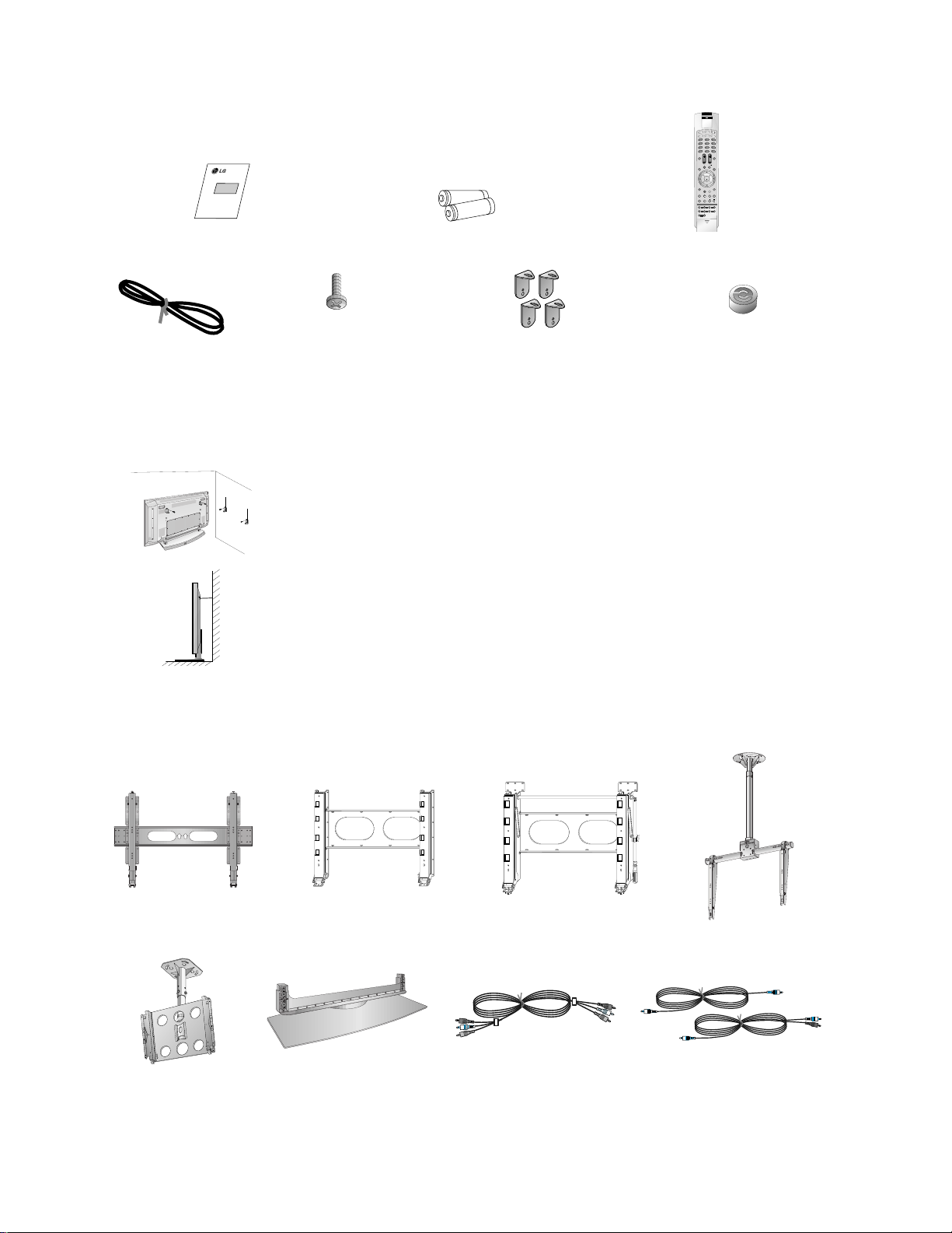
Remote Control handset
- Optional extras can be changed or modified for quality improvement without any notification new optional extras can be
added.
- Contract your dealer for buying these items.
Optional Extras
Accessories
Accessories
Video cables
Audio cables
6-RING SPACER
(Only RZ-60PY10/11 series)
2-TV bracket bolts
(Only RZ-60PY10/11 series
: 6-TV bracket bolts)
Desktop stand (optional)
Ceiling mounting bracket
Wall mounting bracket
(Only RZ-60PY10/11 series)
Tilt wall mounting bracket
(Only RZ-60PY10/11 series)
Tilt wall mounting bracket
404250 40 42 50
Ceiling mounting bracket
40
42
50
42
40
2-TV brackets
2-Wall brackets (optional)
- Secure the TV assembly by joinning it to a wall by using the TV/Wall brackets.
Joinning the TV assembly to the wall to protect the set tumbling
• After the set must be mounted on s desk top, install the TV brackets on the TV as shown.
Insert the 2 bolts and tighten securely, in the upper holes on the bracket.
Install the wall brackets on the wall with 4 bolts*, (not supplied with the product), as shown.
Match the height of the TV brackets and the wall brackets.
Check to be sure the brackets are tightened securely.
• Secure the TV assembly to the wall with strong strings or wound wire cables, (not supplied
with the product), as shown.
Page 13
- 13 -
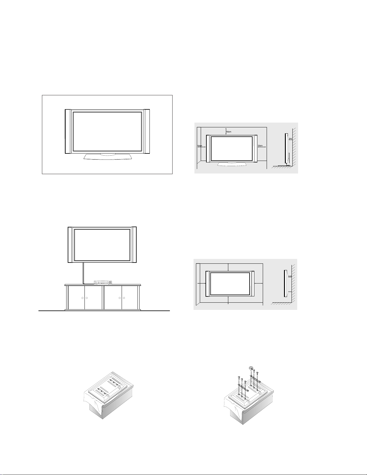
Installation Options
Installation Options
Desktop Pedestal Installation
• The set can be mounted on a desk as shown above. (For further information, refer to the optional 'Desktop Stand
Installation and Setup Guide'.)
• Speakers and speaker stands shown are optional, and are shown for example only.
• The set can be installed in different ways such as on a wall, or on a desktop etc.
Wall Mount: Horizontal Installation
• The set can be installed on a wall as shown above. (For further information, refer to the optional ‘Wall Mounting
Bracket Installation and Setup Guide’.)
• Speakers are optional, and are shown for illustration only.
To Mount on a Wall
Wall mount minimum allowable clearances for adequate ventilation.
To Install on a Desktop
Pedestal mount minimum allowable clearances for
adequate ventilation.
1. Put the RING SPACER in the holes of the bolts before con-
necting to the wall mounting bracket.
2. When you connect the wall mounting bracket to the set,
connect to it by using the bolts, (supplied with the product),
as shown.
• Install the RING SPACER with the bolts on the set as shown. (Only RZ-60PY10/11 series)
10cm
10cm
10cm
10cm
3cm
Page 14
SPECIFICATIONS
NOTE : Specifications and others are subject to change without notice for improvement
.
- 14 -
V Application Range
This spec is applied to the 42”PDP TV used RF-043B Chassis.
V Specification
Each part is tested as below without special appointment.
1) Temperature : 25
¡ 5°C (77¡ 9°F)
2) Relative Humidity: 65¡ 10%
3) Power Voltage: Standard Input voltage (100V-240V~ 50/60Hz)
* Standard Voltage of each product is marked by models.
4) Specification and performance of each parts are followed each drawing and specification by part number in
accordance with BOM.
5)
The receiver must be operated for about 20 minutes prior to the adjustment
.
V Test and Inspection Method
1) Performance : LGE TV test method followed.
2) Demanded other specification
Safety: CE, IEC specification
EMC : CE, IEC
V General Specification
1. General Specification
Remark
Safety : IEC/EN60095
EMI : EN55013
EMS : EN55020
Model Name
RZ-60PY10
Market
EU
Remark
PDP
Maker : LG Chemical
LGE SPEC
Maker : LG(innotek)
Specification
50 inch wide Color Display Module
16:9
PDP60X5xxxx, RGB Closed Type
45% Total light transmittance (E- Mesh)
1) Temp : 0~40 deg
2) Humidity : 0~85%
1) Temp : -20~60 deg
2) Humidity : 0~85%
100 - 240V~, 50/60Hz
No
1
2
3
4
5
6
7
Item
Display Screen Device
Aspect Ratio
PDP Module
Screen Filter
Operating Environment
Storage Environment
Input Voltage
Page 15
2. Model Specification
Item
Market
Broadcasting
Receiving system
Scart Jack (3EA)
Video Input (2EA)
S-Video Input(2EA)
Component Input(1EA)
RGB Input(1EA)
DVI Input(1EA)
Audio Input(4EA)
Wired Control
Specification
EU
PAL B/G/I/D/K, SECAM L/L’
Upper Heterodyne
PAL, SECAM
PAL, SECAM, NTSC
PAL, SECAM, NTSC
Y/Cb/Cr, Y/Pb/Pr
RGB-PC
DVI-PC
PC Audio, Component, AV(2EA)
Discrete IR
Remark
4 System :
PAL B/G/I/D/K, SECAM L, NTSC4.43,PAL60
4 System :
PAL B/G/I/D/K, SECAM L, NTSC4.43,PAL60
DVI-D
L/R Input
- 15 -
No
8
9
10
11
12
13
14
15
16
17
18
Page 16

- 16 -
ADJUSTMENT INSTRUCTIONS
1. Application Object
These instructions apply to the RF-043A Chassis.
2. Specification
(1) Because this is not a hot chassis, it is not necessary to use
an isolation transformer. However, the use of isolation
transformer will help protect test instrument.
(2) Adjustment must be done in the correct order.
(3) The adjustment must be performed in the circumstance of
25±5°C of temperature and 65±10% of relative humidity if
there is no specific designation.
(4) The input voltage of the receiver must keep 100~220V,
50/60Hz.
(5) The receiver must be operated for about 15 minutes prior
to the adjustment.
O After RGB Full white HEAT-RUN Mode, the receiver must
be operated prior to adjustment.
O Enter into HEAT-RUN MODE
1) Press the POWER ON KEY on R/C for adjustment.
2) OSD display and screen display 100% full WHITE
PATTERN.
[ Set is activated HEAT-RUN without signal generator in
this mode.
[ Single color pattern(RED/BLUE/GREEN) of HEAT-RUN
mode uses to check PANEL.
Caution) If you turn on a still screen more than 20 minutes
(Especially digital pattern, cross hatch pattern), a after
image may be occur in the black level part of the
screen.
3. Channel memory
3-1. Setting up the LGIDS
(1) Install the LGIDS. (idsinst.exe)
After installation is completed, check if the file shown on
(Fig. 1) has been created.
After using the right mouse button to click on ‘LGIDS’,
(2) select ‘Create Shortcut’ from the menu with the left mouse
button and move the shortcut icon onto the desktop.
(3) Double-click on the ‘LGIDS’ icon on the desktop to execute
the program.
3-2. Channel memory Method
(1) Check if ‘Malibu’ has been selected on ‘Model’.
(2) Check if ‘Connection’ under ‘Communication’ is ‘OK’.
(3) If it is ‘NG’ , look on ‘PORT’(COM1,2,3...) and make sure
that it’s on the right port.
(4) After connecting RS-232C cable, turn on the power.
If it the communication has been done correctly, ‘READY’
is displayed at the lower right corner of the window shown
as (Fig. 2).
[ When the TV SET is not assembled completely and only
the PCB is supplied by Stand-by 5V, download at the
Stand-by state (LED is Red).
(5) Select proper CH_memory file(*.nvm) for each model at
[NVRAM Download]
$ [Write Batch]
Next, select proper binary file(*.bin) including the CH
information for each model at [NVRAM File].
(6) Click the [Download] button.
It means the completion of the CH memory download if all
items show ‘OK’ and Status is changed by ‘PASS’ at the
lower right corner of the window.
(7) If you want to check whether the CH information is
memorized correctly or not, click the [Verify] button.
And then compare NVRAM File(*.bin) with the CH
information downloaded.
(Fig. 1)
(Fig. 2)
Page 17

- 17 -
4. HDCP Download
4-1. LGIDS Setting Method
(1) Click on ‘setup’ to install in your directory.
(2) After installation is completed, check if the file shown on
(Fig. 4) has been created.
(3) Copy the KEY from source CD into the HDCP directory
which was installed just now.
(DVI_orderNo_2003_data)
(4) After running HDCP(application program) which is inside
the HDCP directory, setup the Communication.
Port : COM1(modification possible)
BaudRate : 115200
4-2. KEY Generation
(1) Click on ‘Key Generation (G)’.
(2) Input the number of the key in Generation count.
ex) If 100 Keys are required, then just register 100 and
next time it will automatically get 101.
(3) Input file : When installing the program for the first time,
you must find the original KEY that you copied and open it.
It is crucial that you copy the original KEY into this
directory.
When you use Generation, the information is recorded in
Config.ini.
(4) Click on ‘Generation’ ———————————————(1)
If it is done correctly, you will see “Job is Success.”——(2)
Click on ‘close’——————————————————(3)
(5) Check the Generation Data(Confirmation it’s possible
within HDCP\CreatedKeyFile)
(Fig. 3)
(Fig. 5)
(Fig. 6)
(Fig. 4)
Page 18
- 18 -
(6) It is possible to check how many Generations are created
at this point.
(Fig. 7) shows that you have created 130 Generations and
you will start from 131 next time.
4-3. HDCP Download Method
(1) Input power of Stand-By 5V.
(Download must be executed only when it is on Stand-by)
(2) The RS-232C(9PIN) must be connected to the COM1 on
the PC.
(3) If all the preparation is completed, click on ‘Download’.
(4) If abnormal state (Fig. 10) display then (3) execute.
5. POWER PCB Assy Voltage
Adjustments
(Va, Vs Voltage Adjustments)
5-1. Test Equipment :D.M.M. 1EA
5-2. Connection Diagram for Measuring
Refer to (Fig 11).
5-3. Adjustment Method for
P/No. 3501V00180A B/D
(1) Va Adjustment
1) After receiving 100% Full White Pattern, HEAT RUN.
2) Connect + terminal of D.M.M to Va pin of P805, connect
- terminal to GND pin of P805.
3) After turning RV501, voltage of D.M.M adjustment as
same as Va voltage which on lable of panel right/top
(Deviation; ±0.5V)
(2) Vs Adjustment
1) Connect + terminal of D.M.M to Vs pin of P805, connect
– terminal to GND pin of P805.
2) After turning RV401, voltage of D.M.M adjustment as
same as Va voltage which on label of panel right/top.
(Deviation; ±0.5V)
(Fig. 7)
(Fig. 8)
(Fig. 9) Normal State
(Fig. 10) Abnormal State
Each PCB assembly must be checked by check JIG set.
(Because power PCB Assembly damages to PDP Module,
especially be careful)
Page 19

- 19 -
5-4. Adjustment Method for
P/No. 3501V00182A B/D
(1) Va Adjustment
1) After receiving 100% Full White Pattern, HEAT RUN.
2) Connect + terminal of D.M.M to Va pin of P805, connect
- terminal to GND pin of P805.
3) After turning RV601, voltage of D.M.M adjustment as
same as Va voltage which on lable of panel right/top
(Deviation; ±0.5V)
(2) Vs Adjustment
1) Connect + terminal of D.M.M to Vs pin of P805, connect
– terminal to GND pin of P805.
2) After turning RV401, voltage of D.M.M adjustment as
same as Va voltage which on label of panel right/top.
(Deviation; ±0.5V)
6. DDC Data Input
6-1. Required Test Equipment
(1) A jig for adjusting PC, DDC (PC serial to D-sub
Connection equipment)
(2) S/W for writing DDC (EDID Data Write & Read)
(3) D-sub 15P Cable, D-Sub to DVI Connector (Connect to
DVI Jack)
6-2. Setting of Device
6-3. Preparation for Adjustment
(1) Set devices as above and turn the PC, jig on.
(2) Put S/W for writing DDC (EDID data Write & Read) into
operation. (operated in DOS mode.)
6-4. Sequence of Adjustment
(1) DDC Data Input for Analog-RGB
1) Put the set on the table and turn the power on.
2) Connect PC Serial to D-sub 15P Cable of jig for DDC
adjustment to RGB terminal (D-Sub 15Pin).
3) Operate S/W for DDC record and select DDC data for
Analog RGB in Model Menu.
4) Operate EDID Write command.
5) Operate EDID Read command and check whether
Check Sum is 53.
6) If Check Sum is not 53, repeat 3) ~ 4).
7) If Check Sum is 53, DDC data for Analog-RGB input is
completed.
(2) DDC Data input for Digital-RGB(DVI)
1) Connect PC Serial to DVI Cable of jig for DDC
adjustment to DVI terminal (DVI Jack).
2) Operate S/W for DDC record and select DDC data for
digital RGB in model menu.
3) Operate EDID Write command.
4) Operate EDID Read command and check whether
Check sum is D2(1page), BF(2page).
5) If Check sum is not D2(1page), BF(2page), repeat 3) ~
4).
6) If Check sum is D2(1page), BF(2page), DDC data for
Analog-RGB input is completed.
< 3501V00180A >
< 3501V00182A >
(Fig. 11) Connection Diagram of Power Adjustment for
Measuring
Page 20

- 20 -
7. Adjustment of White Balance
7-1. Required Equipment
Color Analyzer (CA-100 or same product)
7-2. Connection Diagram of Equipment for
Measuring
7-3. Adjustment of White Balance
O Operate the Zero-calibration of the CA-100, then stick
sensor to PDP module surface when you adjust.
O For manual adjustment, it is also possible by the following
sequence.
(1) Select white pattern of heat-run mode by pressing power
on key on remote control for adjustment then operate heat
run more than 15 minutes.
(2) Supply Gray Pattern (216 Level Full Size Pattern: Signal
level=0.59V±0.03V) signal to VIDEO input. (AV2 Input
60Hz) (Refer to Fig. 12)
(3) Press the FRONT-AV KEY on R/C for converting input
mode.
(4) To adjust, stick sensor to 216 Gray Level Pattern, press
ADJ key twice(White Balance) on remote control.
For adjustment and
D, E on remote control for adjustment
mode to select Red Gain and Green Gain, press VOL +, Key and adjust it until color coordination becomes as
below.
[ 216 Gray level=Signal level 0.59V±0.03V
X; 0.283±0.003, Y; 0.297±0.003
Color Temperature; 9,300°K±500°K
(5) Exit adjustment mode using
A Key.
8. Auto Component Color Balance
8-1. Required Test Equipment
Pattern Equipment: MSP3240A or same product
(16 Gray Scale Pattern output(Component output Level:
0.7Vp-p)
8-2. Method of Auto RGB Color Balance
(1) Input RGB Source : Component 480p/576p 16 Gray Scale
Pattern
At this time, except Pb and Pr signal, only Y signal insert.
(2) Press ADJ KEY on R/C for adjustment.
(3) Press Vol. + KEY and operate To set.
(4) Auto-RGB OK means completed adjustment.
9. Auto RGB Color Balance
9-1. Required Test Equipment
Pattern Equipment: PC Pattern Generator (VG828, VG854,
801GF, MSP3240A)
(16 Gray Scale Pattern output(RGB output Level: 0.7Vp-p)
9-2. Method of Auto RGB Color Balance
(1) Input RGB Source : 16 Gray Scale Pattern output (RGB
output Level : 0.7Vp-p)
(2) Press ADJ KEY on R/C for adjustment.
(3) Press Vol. + KEY and operate To SET.
(4) Auto-RGB OK means completed adjustment.
10. Auto Adjustment Map(RS-232C)
Window
MSPG-2100 or
MSTG-5200
AV Signal Input
Full Size Pattern
216 Gray Level
RS-232C Serial Communication
60Hz
(Fig. 12) White Balance Adjustment
(Fig. 13) Auto RGB/ Component Color Balance Test Pattern
Type
Baud Rate
115200
Index
R Gain
G Gain
B Gain
R Offset
G Offset
B Offset
Data bit
8
Cmd1 Cmd2
j a
j b
j c
j d
j e
j f
Stop bit
1
Parity
NONE
RF-043A
Protocol
Setting
Data Min Value
00(00)
00(00)
00(00)
00(00)
00(00)
00(00)
Max Value
255(FF)
255(FF)
255(FF)
255(FF)
255(FF)
255(FF)
RS232
Page 21

- 21 -
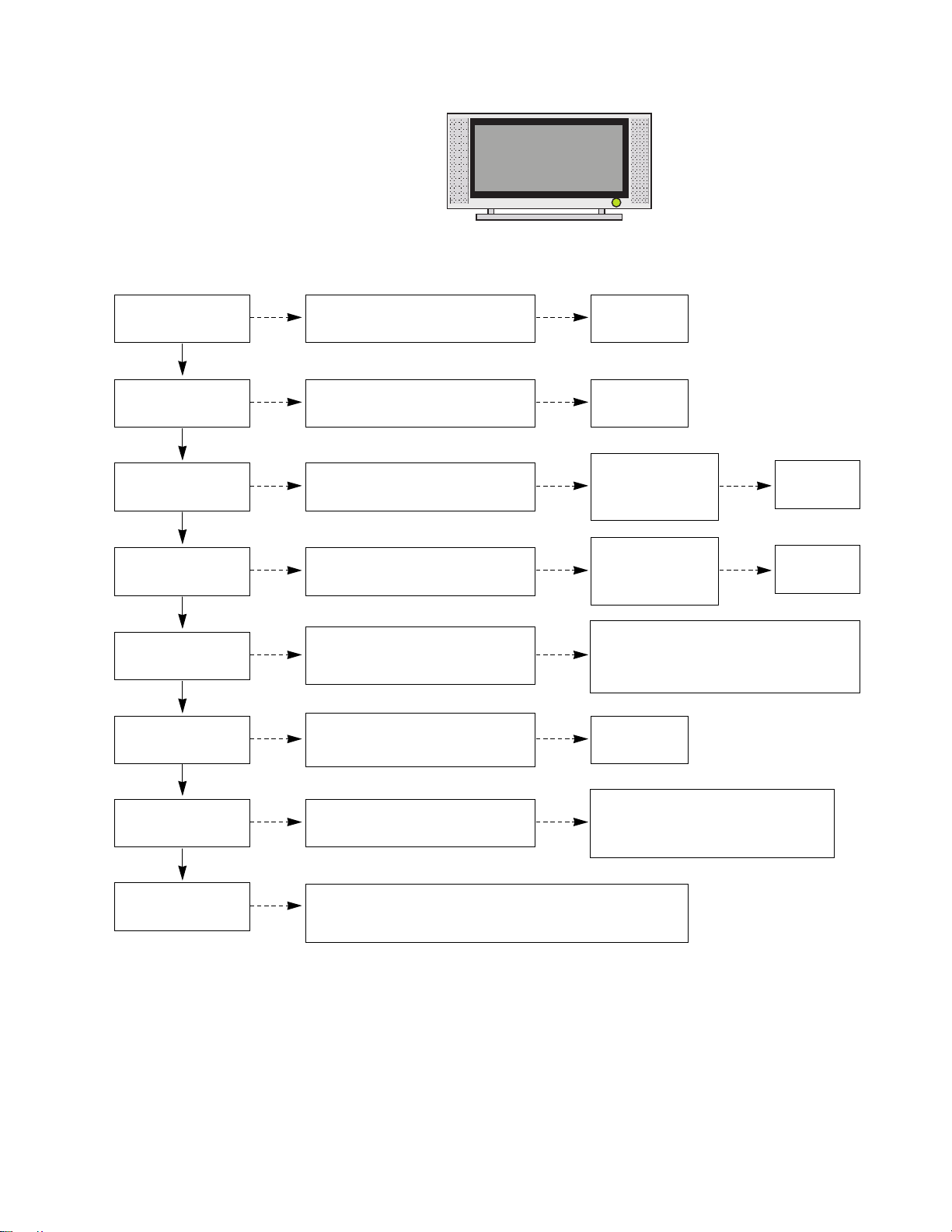
TROUBLE SHOOTING GUIDE
1. Power Board
1-1. The whole flowchart which it follows in voltage output state
Start check
Manufacture enterprise
meaning of a passage
1. Check the Power Off
condition.
Doesn't the
screen whole come
out?
It is identical
with Power Off
condition?
Yes
Yes
No
No
No
No
No
2. Check the Interface
signal condition.
Is the Interface
signal operated?
Yes
3. Check the St-by 5V
signal circuit.
Doesn't the
low pressure output
come out?
Doesn't the
St-by 5V signal
come out?
Yes
Yes
No
4. Check the 5V Monitor
signal circuit.
Doesn't the
5V Monitor signal
come out?
Yes
7. Check the VSC Vs-ON
signal
Doesn't the
high tension output
come out?
Doesn't the
VSC signal Vs-ON
come out?
Yes
Yes
High tension
output voltage Drop
it occurs?
When
remove the
Y B/D Module
Input Connector, output
voltage Drop
it occurs?
When remove
the Y, Z B/D Module
Input Connector, Power
Board high tension output
voltage Drop
it occurs?
Yes No No
9. Check the Power
Board Output high
tension circuit
Yes
10. Check the Z B/D
Module Coutput circuit
Yes
When
remove the
Z B/D Module
Input Connector, output
voltage Drop
it occurs?
11. Check the Y B/D
Module Coutput circuit
Yes
No
8. Check the Vs, Va
voltage output circuit.
Doesn't the
Vs, Va voltage output
come out?
Yes
No
No
5. Check the VSC RL-ON
signal.
Doesn't the
VSC signal RL-ON
come out?
Yes
6. Check the VSC low
pressure output
Doesn't the
VSC low pressure
output come out?
Yes
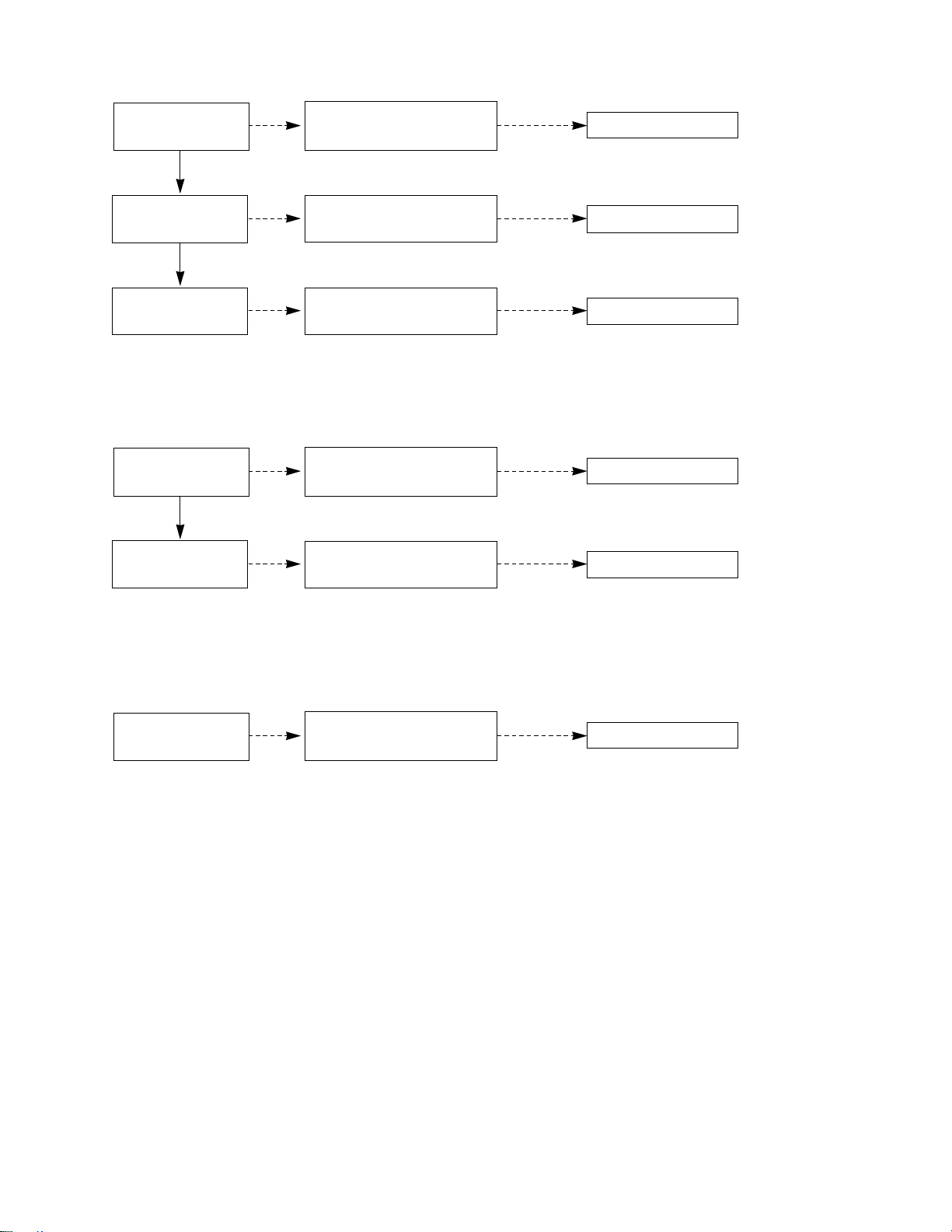
Page 22

- 22 -
1-2. Sony Power Board Structure
T502: Vs Trans
T702: Va Trans
T101: St-by Trans
T103: Low Voltage Trans
1 2 3
Page 23

- 23 -
1-3. Sanken Power Board Structure
T221: Vs Trans
T271: Va Trans
T121: St-by Trans
T201: Low Voltage Trans
1 2 3
Page 24

- 24 -
2. No Power
(1) Symptom
¯ Does’t minute discharge at module.
¯ Non does not come in into the front LED.
(2) Check follow
Is plug in power cord? Plug in power cord.
Yes
No
Is connect the Line Filter and Power
Switch Cable?
Connect Cable.
Yes
No
Is connect the Power Switch and
Power Board Cable?
Connect Cable.
Yes
No
Is normal the Fuse(F101) on Power
Board?
Replace Fuse.
Yes
No
Is connect the Power Board and 7P
of VSC Board Cable?
Connect Cable.
Yes
No
Is connect the Power Switch and
Power Board Cable?
After remove the cable connect to
Power Board(except the CN101
connection cable), authorizes the
AC voltage marking on manual.
When ST-BY 5V does not operate,
replace Power Board.
Connect Cable.
Yes
No
Page 25

- 25 -
3. Protect Mode
(1) Symptom
¯ After once shining, it does not discharge minutely
from module
¯ The Rely falls(The sound is audible “click”)
¯ It is converted with the color where the front LED
is red from green.
(2) Check follow
Is normal the Power
Board?
Replace Power
Board.
Is output the normality Low/High
voltage except Stand-by 5V?
Yes
No
No
Is normal the each
connector?
Replace
connector.
Replace
Y-Board.
After connecting well each connector,
the normality it operates?
Yes
No
No
Is normal the
Ctrl Board?
Replace
X-Board.
Is normal the output voltage after
remove P1, 2, 101, 300, 701, 702
connector of Ctrl-B/D?
Yes
No
Yes
Is normal the
Y- Board?
Is normal the output
voltage after remove
P5, P6 connector of
Y-B/D?
Is normal the Fuse(F52) on Y-B/D?
(In case of open is replace)
Yes
No
Yes Yes
Replace
Z-Board.
Is normal the
Z- Board?
Is normal the output
voltage after remove
P1 connector of
Z-B/D?
Is normal the Fuse(FS1, FS2) on Z-
B/D? (In case of open is replace)
Yes
No
Yes
Is normal the
X- Board?
Is normal the output voltage after
remove P1, 2, 3, 4, 6, 7 connector of
X-B/D?
After remove P1, P2, P3, P4 output voltage
normality: Replace Right X-B/D
After remove P6, P7 output voltage
normality: Replace Left X-B/D
Yes
No
Yes
Is normal the
VSC Board?
Is normal the output voltage after
remove P1000, P1200?
After crisis COF of each board, check the normality operates.
If in case normality operates, correspondence COF Fail is
replace the module.
After remove P1000 normal operation:
Replace Analog Board
After remove P1200 normal operation:
Replace Digital Board
Yes
No
Is normal the
COF of X, Y, Z?
No
Yes
Yes
Page 26
- 26 -
4. No Raster
(1) Symptom
¯ Does’t minute discharge at module.
¯ It maintains the condition where the front LED is green.
(2) Check follow
Is normal the Power
Board?
Replace Power
Board.
Is output the normality Low/High
voltage except Stand-by 5V?
Yes
No
No
Is normal the each
connector?
Replace
connector.
Replace
Y-Board.
After connecting well each connector,
the normality it operates?
Yes
No
No
Is normal the
Ctrl Board?
Replace
X-Board.
Is normal the output voltage after
remove P1, 2, 101, 300, 701, 702
connector of Ctrl-B/D?
Yes
No
Yes
Is normal the
Y- Board?
Is normal the output
voltage after remove
P5, P6 connector of
Y-B/D?
Is normal the Fuse(F52) on Y-B/D?
(In case of open is replace)
Yes
No
Yes Yes
Replace
Z-Board.
Is normal the
Z- Board?
Is normal the output
voltage after remove
P1 connector of
Z-B/D?
Is normal the Fuse(FS1, FS2) on Z-
B/D? (In case of open is replace)
Yes
No
Yes
Is normal the
X- Board?
Is normal the output voltage after
remove P1, 2, 3, 4, 6, 7 connector of
X-B/D?
After remove P1, P2, P3, P4 output voltage
normality: Replace Right X-B/D
After remove P6, P7 output voltage
normality: Replace Left X-B/D
Yes
No
Yes
Is normal the
VSC Board?
Is normal the output voltage after
remove P1000, P1200?
After crisis COF of each board, check the normality operates.
If in case normality operates, correspondence COF Fail is
replace the module.
After remove P1000 normal operation:
Replace Analog Board
After remove P1200 normal operation:
Replace Digital Board
Yes
No
Is normal the
COF of X, Y, Z?
No
Yes
Yes
Page 27

- 27 -
5. In case of occur strange screen into specific mode
5-1. In case of does’t display the OSD
(1) Symptom
¯ LED is green
¯ The minute discharge continuously becomes
accomplished from module
(2) Check follow
Is normal the LVDS
cable?
Is normal the VSC
Digital Board?
Is the LVDS cable
connected well?
Cable inserts well.
Yes
No
No
Yes
Operates the Thine
IC(IC1100)?
Replace Thine
IC(IC1100).
No
Is normal the Ctrl
Board of Module?
Replace Ctrl B/D.
No
No
Operates the
IEP(IC500)?
Replace
IEP(IC500).
Yes
No
Operates the
Scaler(IC700)?
Replace
Scaler(IC700).
Yes
Replace cable.
Yes
Page 28

- 28 -
5-2. In case of does’t display the screen into specific mode
(1) Symptom
¯ The screen does not become the display from specific input mode
(RF, AV, Component, RGB, DVI).
(2) Check follow
¯ Check the all input mode should become normality display
.
¯ Check the Video(Main)/Data(Sub), Video(Main)/Video(Sub) should become
normality display from the PIP mode or DW mode. (Re-Check it Swap)
(3) In case of becomes unusual display from RF mode
(4) In the case of becomes unusual display from RF, AV mode
Is normal the Tuner?
Is normal the
CXA2069Q?
Is the Tuner Cable
connected well?
Cable inserts well.
Yes
No
No
Yes
Is normal the
VPC3230?
Replace Tuner
No
Is normal the Input voltage, IIC
Communication and CVBS output?
Yes
Is normal the Input voltage, IIC
Communication and HV sync?
No
Replace IC
No
Is normal the Input voltage, IIC
Communication and HV sync?
No
Replace IC
No
Is normal the
CXA2069Q?
Yes
Is normal the
VPC3230?
Is normal the Input voltage, IIC
Communication and HV sync?
No
Replace IC
No
Is normal the Input voltage, IIC
Communication and HV sync?
No
Replace IC
No
Page 29

- 29 -
(5) In the case of becomes unusual display from RF, AV, Component 480i mode
(6) In the case of becomes unusual display from Component DTV mode
Is normal the
VPC3230?
Yes
Is normal the S2300?
Is normal the Input voltage, IIC
Communication and HV sync?
No
Replace IC
No
Is normal the Input voltage, IIC
Communication and HV sync?
No
Replace IC
No
Yes
Is normal the Scaler?
Is normal the Input voltage, IIC
Communication and HV sync?
No
Replace IC
No
Is normal the
74LS123?
Yes
Is normal the
CXA2101?
Is normal the Input voltage, IIC
Communication and HV sync?
No
Replace IC
No
Is normal the Input voltage, IIC
Communication and HV sync?
No
Replace IC
No
Yes
Is normal the
M52758?
Is normal the Input voltage, IIC
Communication and HV sync?
No
Replace IC
No
Yes
Is normal the Scaler?
Is normal the Input voltage, IIC
Communication and HV sync?
No
Replace IC
No
Page 30
- 30 -
(7) In the case of becomes unusual display from RGB DTV mode
(8) In the case of becomes unusual display from RGB PC mode
(8) In the case of becomes unusual display from DVI mode
Is normal the
CXA2101?
Yes
Is normal the
M52758?
Is normal the Input voltage, IIC
Communication and HV sync?
No
Replace IC
No
Is normal the Input voltage, IIC
Communication and HV sync?
No
Replace IC
No
Is normal the
M52758?
Yes
Is normal the Scaler?
Is normal the Input voltage, IIC
Communication and HV sync?
No
Replace IC
No
Is normal the Scaler?
Is normal the Input voltage, IIC
Communication and HV sync?
No
Replace IC
No
Is normal the Input voltage, IIC
Communication and HV sync?
No
Replace IC
No
Yes
Is normal the Scaler?
Is normal the Input voltage, IIC
Communication and HV sync?
No
Replace IC
No
Page 31

- 31 -
6. In case of no sound
(1) Symptom
¯ LED is green
¯ Screen display but sound is not output
(2) Check follow
Is normal the SPK
cable?
Is the SPK cable
connected well?
Cable inserts well.
No
No
Cable inserts well.
No
Replace IC800
No
Replace IC801
No
Replace SPK cable
Yes
Yes
Is normal the
RGB/DVI sound?
Is the Flat cable
connected well?
No
No
Operates the IC800?
Yes
Operates the IC801?
Replace IC802
No
Operates the IC802?
Replace
VSC Analog B/D
Yes
Yes
Yes
Is normal the
RF/AV/Component
sound?
Page 32

- 32 -
BLOCK DIAGRAM
RGB
(
PC/DTV
)
DVI
(
PC/DTV
)
RS232
IR
74ACT253
RX0/1,TX0/1
IR
TX
SCL/SDA
RGB H/ V
SCL/SDA
RX/ TX0/ 1/2, RX/TXC
ST3232C
24LC21
74HCT0
8
24LC21
CXA2101
Scart1
Scart2
Scart3
RF
CVBS
S-VHS
CXA2069Q
SWITCH
Tuner
(
M
)
Tuner
(
S
)
Vin1
(
CVBS
)
VPC3230
(
M
)
Video Decoder
VPC3230
(
S
)
Video Decoder
1H RGB
Vin2
(
CVBS
)
MNT OUT
TV OUT
Vin3
(
CVBS
)
TU_Main
TU_Sub
Vin4
YCin4
Main_V
Main_YC
Main_V
Main_YC
SDA6001
Text Processor
Text_V
HYV641620
SRAM
AM29LV160
F-ROM
74LS123
Comp_480i
M52758F
Switch
S2300
DeInterlacer
YCbCr
/
8
HY57V64322
SDRAM (8MB)
RGB PC/ DTV
RGB PC
RGB DTV
gm1601
Scaler (Malibu)
Comp DTV
CXA_RGB
RGB_Data
Main_Video
/
24
Sub_Video
/
8
DVI_Data
TX_Out
RS232_RX/TX
Comp/ RGB_SW
From Malibu
Digital
Analog
Side -AV
CVBS S-VHS
Vin5
YCin5
Comp_Y
Comp_480I/ P
To Malibu
Video for TextText
TX0/1/ 2/3/ C
Disp_En
SDATA
SCLK, SLE
HY5DU283222A
SDRAM (128MB)
AM29LV
F-ROM
(
1MB
)
Comp
/RGB_SW
Comp_480I/ P
Pos t- processing Block is omitted.
so-called JEPICO, in this case
TMDS TX is also required.
Sound Processing Block Diagram
is separated..
RCA-type Block Diagram is also
separated..
DVI RX
w/HDCP
ADC
w/PLL
IEP
2424 2424
10
WIRE
ZHINE
Comp1
(
D
D/
D
T
V
)
V
BOARD
BOARD
BOARD
BLOCK DIAGRAM
Page 33

- 33 -
RGB
(PC/ DTV)
DVI
(PC/ DTV)
RS232
IR
ST3232C
74ACT253
74HCT08
Tx
gm1501H
24LC21
24LC21
RGB PC
IIS
IIS
IIS
CXA2101CXA2101
RGB DTV
HV
M52758FP
IC202(MUX)
M52758FP
IC202(MUX)
M52758FP
IC204
M52758FP
IC204
RGB_DTV
FLI2300FLI2300
HY57V64322
SDRAM (8MB)
HY57V64322
SDRAM (8MB)
DAC_RGB
Comp1
(
DVD/DT V
)
RF
CVBS IN
Side
S-VHS
Analog
CVBS OUT
Side-CVBS
Comp2
(
DVD/DTV
)
TQFP 128K
DDR Memory
TQFP 128K
DDR Memory
Flash ROM
512K/1M
Flash ROM
512K/1M
M62320FP
(I2C Expender)
M62320FP
(I2C Expender)
CXA2069Q
UPD64083UPD64083
VPC3230
(MAIN)
VPC3230
(MAIN)
VPC3230
(SUB)
VPC3230
(SUB)DVD_SUB
DTV_Comp
M52758FP
IC400(MUX)
M52758FP
IC400(MUX)
DVD_MAIN
DVD2_MAIN
DVD2_SUB
DTV2_Comp
S-VHS
Tuner (M)
Tuner (S)
VIN1
Y/ CIN1
Comp
Comp2
MNT_OUT
VIN2
Y/ CIN2
MAIN_VOUT
SUB_COUT
SUB_YOUT
CAB_VIN
MAIN_YOUT
MAIN_COUT
LA7151M
SW CVBS/ Y
COMB_YOUT
COMB_COUT
ALT_Y_480I_MAIN
ALT_Y_480I_SUB
ALT_Y2_480I_MAIN
ALT_Y2_480I_SUB
S/ DVD_Comp
M37136
(OTP)
M37136
(OTP)
CAB_Comb
MAIN_YOUT
M656 8 Bit
S656 8 Bit
Side A/V
TMDS Transfer
/Thine
LVDS
31PIN
RGB_24Bit
Analog
RGB
DVI
VPORT
(24bit)
SVPORT
(16bit)
IEP
ZHINE
WIRE
Digtal
BOARD
BOARD
Page 34

- 34 -
EXPLODED VIEW
551
550
305
300
302
311
301
301
314
314
308
310
313
312
309
307
303
101
102
304
306
570
540
501
560
541
211
210
203
204
205
200
580
206
209
212
400
401
121
120
610
620
208
202
201
520
530
600
630
Page 35

- 35 -
101 5900V08004A FAN,DC F8025L12B2-RG DONG YANG 80MM 12V 120MA 2300RPM 79G L 300MM
102 4980V00A48B SUPPORTER, FAN EGI PRESS DU-60PY10
120 6401VD0017B SPEAKER ASSEMBLY, RZ-60PY10 C/SKD WOOFER TWEETER L
121 6401VD0016B SPEAKER ASSEMBLY, RZ-60PY10 C/SKD WOOFER TWEETER R
200 6348Q-B038S PDP, 60” 16:9 1365*768 PDP60X50554.ADLGA
201 6871QDH035C PWB(PCB) ASSEMBLY,DISPLAY YDRV ASSY HAND INSERT TOP(60X5) SN755866PZP
202 6871QDH036C PWB(PCB) ASSEMBLY,DISPLAY YDRV ASSY HAND INSERT BOTTOM(60X5) SN755866PZP
203 6871QLH046A PWB(PCB) ASSEMBLY,DISPLAY XRLT ASSY HAND INSERT 60X5A X LEFT BOTTOM
204 6871QXH029A PWB(PCB) ASSEMBLY,DISPLAY XRCT ASSY HAND INSERT 60X5A X CENTER BOTTOM
205 6871QRH053A PWB(PCB) ASSEMBLY,DISPLAY XRRT ASSY HAND INSERT 60X5A X RIGHT BOTTOM
206 6871QYH035A PWB(PCB) ASSEMBLY,DISPLAY YSUS ASSY HAND INSERT 60X5A 4LAYER
208 6871QCH055A PWB(PCB) ASSEMBLY,DISPLAY CTRL ASSY HAND INSERT 60X5A, 4023, LVDS”
209 6871QZH040A PWB(PCB) ASSEMBLY,DISPLAY ZSUS ASSY HAND INSERT 60X5A 4LAYER
210 6871QLH045A PWB(PCB) ASSEMBLY,DISPLAY XRLT ASSY HAND INSERT 60X5A LEFT TOP
211 6871QXH028A PWB(PCB) ASSEMBLY,DISPLAY XRCT ASSY HAND INSERT 60X5A X CENTER TOP
212 6871QRH052A PWB(PCB) ASSEMBLY,DISPLAY XRRT ASSY HAND INSERT 60X5A X RIGHT TOP
300 3091V00664A CABINET ASSEMBLY, DN-60PY10 CABINET ASSY(MOLD)
301 4972V00114B FIXER, FRAME EGI DU-60PY10 LEFT PRESS
302 4980V00A94C SUPPORTER, FILTER AL RZ-60PY10 TOP ASSY C/SKD
303 4980V00A97C SUPPORTER, FILTER AL RZ-60PY10 LEFT ASSY C/SKD
304 4980V00A95C SUPPORTER, FILTER AL RZ-60PY10 BOTTOM ASSY C/SKD
305 5230V00022C FILTER(MECH), DU-60PY10 LG-CHEMICAL FLATRON PLASMA DELETE LG FOR AMREICA
306 4980V00A96C SUPPORTER, FILTER AL RZ-60PY10 RIGHT ASSY C/SKD
307 4811V00112A BRACKET ASSEMBLY, SPEAKER DU-60PY10 SPK GRILL ASSY R
308 4811V00113A BRACKET ASSEMBLY, SPEAKER DU-60PY10 SPK GRILLE ASSY L
309 3210V00255A FRAME FRONT SIDE AL DU-60PY10 RIGHT WITH SPK
310 3210V00256A FRAME FRONT SIDE AL DU-60PY10 LEFT WITH SPK
311 3210V00253A FRAME FRONT UPPER AL DU-60PY10 .
312 3790V00745G WINDOW, DECO RZ-60PY10 RIGHT BK PRINT
313 3790V00745H WINDOW, DECO RZ-60PY10 LEFT BK PRINT
314 4972V00113B FIXER, FRAME EGI DU-60PY10 RIGHT PRESS
315 3210V00254C FRAME BOTTOM AL RZ-60PY10
400 3809V00460B BACK COVER ASSEMBLY, RZ-60PY10 BACK COVER ASSY C/SKD
401 3301V00025J PLATE ASSEMBLY, ASSY . VSC TUNER COVER RZ-60PY10 C/SKD
501 3301V00026E PLATE ASSEMBLY, ASSY 3300V00338_339 RZ-60PY10 C/SKD
520 6871VMMS74A PWB(PCB) ASSEMBLY,MAIN RF-043B DIGITAL B/D MANUAL
530 6871VSMZ56A PWB(PCB) ASSEMBLY,SUB TUNER RF043B MALIBU RZ50 SUB ANALOG MANUAL
540 6871VSME94A PWB(PCB) ASSEMBLY,SUB PSW AF044A POWER SWITCH
541 5020V00436D BUTTON, POWER RZ-60PY10 ABS, AF-303S 1KEY SKD
550 6871VSME91A PWB(PCB) ASSEMBLY,SUB A/V RF043A MALIBU SIDE AV
551 4811V00114D BRACKET ASSEMBLY, SIDE AV RZ-60PY10 ASSY C/SKD
560 6871VSMG25A PWB(PCB) ASSEMBLY,SUB CONT RF043B RZ-60PY10 LOCAL_KEY
570 6871VSMF12C PWB(PCB) ASSEMBLY,SUB LED AF044A DN-60PY10 INDEX
580 3501V00193A BOARD ASSEMBLY POWER DN-60PY10 AF044A 9YPSU0001CG LGINNOTEK MAIN B/D
600 6871VSMG21A PWB(PCB) ASSEMBLY,SUB SUB RF043A FAN CTRL
610 3501V00194A BOARD ASSEMBLY, PFC DN-60PY10 AF044A 9YPSU0001BG LGINNOTEK PFC B/D
620 3501V00195A BOARD ASSEMBLY, POWER DN-60PY10 AF044A 9YPSU0001AG LGINNOTEK AC-IN B/D
630 3501V00173B BOARD ASSEMBLY, ASSY AP-60DY10 WITHOUT PACKING SKD
EXPLODED VIEW PARTS LIST
No. Part No. Description
Page 36

M62320FP,I/O EXPANDER 16P SOP TP
AT24C02N-10SI-2.7 ATMEL 8P SOIC
KA7809R, FAIRCHILD 2P D-PAK
MIC39100 MICREL 3P SOT223
PQ05DZ1U SHARP 5, SMD TYPE
TK11840L 8P SOT23L
PQ05DZ1U SHARP 5, SMD TYPE
M62320FP,I/O EXPANDER 16P SOP TP
AT24C02N-10SI-2.7 ATMEL 8P SOIC
SN74HCT08D TEXAS INSTRUMENT 16P
M62320FP,I/O EXPANDER 16P SOP TP
SN74LVTH541PWR 20P TSSOP
SN74LVTH541PWR 20P TSSOP
KA7805R FAIRCHILD 2P D-PAK
THC63LVD103 64P TQFP TRAY 10BIT LVDS TX
SC1565IST-1.8 SEMTECH 3P SOT223 TP
MIC39100 MICREL 3P SOT223
KA7809R, FAIRCHILD 2P D-PAK
BA033FP-E2 ROHM 3P-SOP,TO252-3
PQ05DZ1U SHARP 5, SMD TYPE
PQ05DZ1U SHARP 5, SMD TYPE
BA033FP-E2 ROHM 3P-SOP,TO252-3
SC1565IST-1.8 SEMTECH 3P SOT223 TP
BA033FP-E2 ROHM 3P-SOP,TO252-3
MIC39100 MICREL 3P SOT223
74ACT253SC FAIRCHILD 16P SOIC
ST3232CDR SGS-THOMSON SOP16
M52758FP MITSUBISHI 36PIN
M74HC123RM13TR SGS-THOMSON 16P SOP
M74HC123RM13TR SGS-THOMSON 16P SOP
CXA2069Q QFP64 BK I2C BUS AV S/W
CXA2101AQ 80P,QFP BK
SN74HCT08D TEXAS INSTRUMENT 16P
M74HC123RM13TR SGS-THOMSON 16P SOP
LGDP4410 LG IC 176P TQFP TRAY IEP
SDA6001 QH B12 MICRONAS 128P MQFP
KIA7805API 3P TO-220 ST 5V(=KIA7805PI)
PQ09RD21 4SIP ST REGULATOR
PQ09RD21 4SIP ST REGULATOR
PQ12RD21 4SIP ST REGULATOR
M62320FP,I/O EXPANDER 16P SOP TP
DS1621V 8P SOIC ST THERMOSTAT HY57V641620HGT-H HYNIX 54P TSOPII
MX29LV160ATTC-70 MACRONIX 48P TSOP
AT24C16AN-10SI-2.7 ATMEL 8P SOIC
KIA7027AF 3, SOT-89 TP RESET IC 2.7V
VPC3230D C5 80P QFP
FLI2300BD GENESIS 208P PQFP
HY57V643220C(L)T-6 HYNIX 86P TSOP
VPC3230D C5 80P QFP
GM1501HBD GENESIS 416P PBGA
REPLACEMENT PARTS LIST
LOCA. NO PART NO DESCRIPTION
IC701
IC702
IC800
IC800
IC801
IC801
IC802
IC803
IC805
Q100
Q100
Q1000
Q101
Q101
Q102
Q102
Q102
Q103
Q103
Q103
Q104
Q105
Q105
Q106
Q106
Q107
Q107
Q108
Q108
Q109
Q109
Q110
Q110
Q111
Q111
Q112
Q113
Q114
Q1200
Q1201
Q1202
Q1501
Q1503
Q207
Q208
Q209
Q210
Q211
Q214
Q215
Q216
0IMMRAL025A
0IKE704200J
0IMCRMN028A
0IMMRHY020B
0IMCRNL001A
0IMMRMR023A
0IMCRTI028C
0IPRPJR017A
0IKE704200J
0TR150400BA
0TR830009BA
0TRKE80038A
0TR387500AA
0TR830009BA
0TR387500AA
0TR387500AA
0TR830009BA
0TR150400BA
0TR387500AA
0TR830009BA
0TR387500AA
0TR387500AA
0TR387500AA
0TR150400BA
0TR387500AA
0TR387500AA
0TR387500AA
0TR150400BA
0TR387500AA
0TR150400BA
0TR387500AA
0TR387500AA
0TR830009BA
0TR387500AA
0TR830009BA
0TR387500AA
0TR387500AA
0TR387500AA
0TR387500AA
0TR387500AA
0TR387500AA
0TR830009BA
0TR830009BA
0TR387500AA
0TR387500AA
0TR150400BA
0TR387500AA
0TR104009AF
0TR387500AA
0TR150400BA
0TR104009AF
AT24C32AN-10SI-2.7 ATMEL 8PIN SOP TP 32K 3.3V
KIA7042AF SOT-89 TP 4.2V VOLTAGE DETECTOR
MSP4410G-QA-C13-101
HY5DU283222AQ-5 HYNIX 100P LQFP
NSP-6241B NEOFIDELITY 64P TQFP
MX29LV800TTC-70 MACRONIX 48PIN
TAS5122DCAR 56P/TSSOP
NJU26901E2 JRC 8P,EMP
KIA7042AF SOT-89 TP 4.2V
CHIP 2SA1504S(ASY) KEC
BSS83 TP PHILIPS NON N-CHANNEL S/W TR
KTC3552T-RTK KEC SOT-23F 50V 3A
CHIP 2SC3875S(ALY) KEC
BSS83 TP PHILIPS NON N-CHANNEL S/W TR
CHIP 2SC3875S(ALY) KEC
CHIP 2SC3875S(ALY) KEC
BSS83 TP PHILIPS NON N-CHANNEL S/W TR
CHIP 2SA1504S(ASY) KEC
CHIP 2SC3875S(ALY) KEC
BSS83 TP PHILIPS NON N-CHANNEL S/W TR
CHIP 2SC3875S(ALY) KEC
CHIP 2SC3875S(ALY) KEC
CHIP 2SC3875S(ALY) KEC
CHIP 2SA1504S(ASY) KEC
CHIP 2SC3875S(ALY) KEC
CHIP 2SC3875S(ALY) KEC
CHIP 2SC3875S(ALY) KEC
CHIP 2SA1504S(ASY) KEC
CHIP 2SC3875S(ALY) KEC
CHIP 2SA1504S(ASY) KEC
CHIP 2SC3875S(ALY) KEC
CHIP 2SC3875S(ALY) KEC
BSS83 TP PHILIPS NON N-CHANNEL S/W TR
CHIP 2SC3875S(ALY) KEC
BSS83 TP PHILIPS NON N-CHANNEL S/W TR
CHIP 2SC3875S(ALY) KEC
CHIP 2SC3875S(ALY) KEC
CHIP 2SC3875S(ALY) KEC
CHIP 2SC3875S(ALY) KEC
CHIP 2SC3875S(ALY) KEC
CHIP 2SC3875S(ALY) KEC
BSS83 TP PHILIPS NON N-CHANNEL S/W TR
BSS83 TP PHILIPS NON N-CHANNEL S/W TR
CHIP 2SC3875S(ALY) KEC
CHIP 2SC3875S(ALY) KEC
CHIP 2SA1504S(ASY) KEC
CHIP 2SC3875S(ALY) KEC
CHIP KRC104S SOT-23 TP KEC
CHIP 2SC3875S(ALY) KEC
CHIP 2SA1504S(ASY) KEC
CHIP KRC104S SOT-23 TP KEC
LOCA. NO PART NO DESCRIPTION
IC100
IC100
IC1000
IC1001
IC1002
IC1003
IC1004
IC101
IC101
IC102
IC102
IC103
IC104
IC105
IC1100
IC1200
IC1201
IC1202
IC1300
IC1301
IC1302
IC1303
IC1304
IC1305
IC1306
IC200
IC201
IC202
IC203
IC204
IC400
IC401
IC402
IC403
IC500
IC500
IC5001
IC5002
IC5003
IC5004
IC5005
IC5006
IC501
IC502
IC503
IC504
IC600
IC600
IC601
IC700
IC700
0IMI623200B
0IMMRAL014B
0IMCRFA010A
0IPRPML001A
0IMCRSH001A
0ITK118100B
0IMCRSH001A
0IMI623200B
0IMMRAL014B
0IMCRTI003A
0IMI623200B
0IMCRTI021A
0IMCRTI021A
0IMCRFA015A
0IMCRTH002A
0IMCRSJ001A
0IPRPML001A
0IMCRFA010A
0IMCRRH001A
0IMCRSH001A
0IMCRSH001A
0IMCRRH001A
0IMCRSJ001A
0IMCRRH001A
0IPRPML001A
0IFA742530B
0IMCRSG010A
0IMCRMI006A
0ISTLSG009A
0ISTLSG009A
0ISO206900A
0ISO210100B
0IMCRTI003A
0ISTLSG009A
0ICTMLG018A
0IMCRMN023A
0IKE780500Q
0ISH092100B
0ISH092100B
0ISH122100B
0IMI623200B
0IDS162100B
0IMMRHY001F
0IMMRMR006B
0IMCRAL006A
0IKE702700D
0IIT323000E
0IMCRGN002C
0IMMRHY033A
0IIT323000E
0IPRPGN012A
IC
TRANSISTOR
- 36 -
Page 37

- 37 -
LOCA. NO PART NO DESCRIPTION
Q217
Q218
Q219
Q300
Q301
Q302
Q303
Q304
Q305
Q306
Q307
Q308
Q309
Q310
Q311
Q312
Q313
Q314
Q315
Q316
Q400
Q400
Q401
Q401
Q402
Q402
Q403
Q403
Q404
Q405
Q406
Q800
Q801
Q802
D100
D100
D1000
D1001
D1002
D1003
D1004
D101
D101
D102
D105
D106
D116
D117
D118
D119
0TR387500AA
0TR387500AA
0TR387500AA
0TR387500AA
0TR387500AA
0TR387500AA
0TR387500AA
0TR387500AA
0TR387500AA
0TR387500AA
0TR387500AA
0TR387500AA
0TR387500AA
0TR387500AA
0TR387500AA
0TR387500AA
0TR387500AA
0TR387500AA
0TR387500AA
0TR387500AA
0TR150400BA
0TR387500AA
0TR150400BA
0TR387500AA
0TR150400BA
0TR387500AA
0TR387500AA
0TR387500AA
0TR387500AA
0TR387500AA
0TR387500AA
0TR387500AA
0TR387500AA
0TR387500AA
0DD226239AA
0DD226239AA
0DD226239AA
0DD184009AA
0DD226239AA
0DD226239AA
0DD226239AA
0DD226239AA
0DD226239AA
0DD226239AA
0DD184009AA
0DD184009AA
0DD226239AA
0DD226239AA
0DD226239AA
0DD226239AA
CHIP 2SC3875S(ALY) KEC
CHIP 2SC3875S(ALY) KEC
CHIP 2SC3875S(ALY) KEC
CHIP 2SC3875S(ALY) KEC
CHIP 2SC3875S(ALY) KEC
CHIP 2SC3875S(ALY) KEC
CHIP 2SC3875S(ALY) KEC
CHIP 2SC3875S(ALY) KEC
CHIP 2SC3875S(ALY) KEC
CHIP 2SC3875S(ALY) KEC
CHIP 2SC3875S(ALY) KEC
CHIP 2SC3875S(ALY) KEC
CHIP 2SC3875S(ALY) KEC
CHIP 2SC3875S(ALY) KEC
CHIP 2SC3875S(ALY) KEC
CHIP 2SC3875S(ALY) KEC
CHIP 2SC3875S(ALY) KEC
CHIP 2SC3875S(ALY) KEC
CHIP 2SC3875S(ALY) KEC
CHIP 2SC3875S(ALY) KEC
CHIP 2SA1504S(ASY) KEC
CHIP 2SC3875S(ALY) KEC
CHIP 2SA1504S(ASY) KEC
CHIP 2SC3875S(ALY) KEC
CHIP 2SA1504S(ASY) KEC
CHIP 2SC3875S(ALY) KEC
CHIP 2SC3875S(ALY) KEC
CHIP 2SC3875S(ALY) KEC
CHIP 2SC3875S(ALY) KEC
CHIP 2SC3875S(ALY) KEC
CHIP 2SC3875S(ALY) KEC
CHIP 2SC3875S(ALY) KEC
CHIP 2SC3875S(ALY) KEC
CHIP 2SC3875S(ALY) KEC
CHIP KDS226 SOT-23
CHIP KDS226 SOT-23
CHIP KDS226 SOT-23
KDS184S CHIP 85V 300MA KEC TP
CHIP KDS226 SOT-23
CHIP KDS226 SOT-23
CHIP KDS226 SOT-23
CHIP KDS226 SOT-23
CHIP KDS226 SOT-23
CHIP KDS226 SOT-23
KDS184S CHIP 85V 300MA KEC TP
KDS184S CHIP 85V 300MA KEC TP
CHIP KDS226 SOT-23
CHIP KDS226 SOT-23
CHIP KDS226 SOT-23
CHIP KDS226 SOT-23
LOCA. NO PART NO DESCRIPTION
D120
D1200
D1201
D1206
D121
D122
D123
D124
D125
D126
D127
D128
D129
D130
D1300
D1301
D1302
D1303
D1304
D1305
D1306
D131
D1501
D1503
D200
D201
D202
D203
D204
D205
D400
D500
D5001
D501
D502
D503
ZD100
ZD101
ZD102
ZD103
ZD104
ZD105
ZD206
ZD207
ZD208
ZD400
ZD401
ZD800
C1001
C1002
0DD226239AA
0DD226239AA
0DD226239AA
0DD226239AA
0DD226239AA
0DD226239AA
0DD226239AA
0DD226239AA
0DD226239AA
0DD226239AA
0DD226239AA
0DD226239AA
0DD226239AA
0DD226239AA
0DD226239AA
0DD226239AA
0DD226239AA
0DD226239AA
0DD226239AA
0DD226239AA
0DD226239AA
0DD226239AA
0DD226239AA
0DD226239AA
0DD226239AA
0DD226239AA
0DD226239AA
0DD226239AA
0DD226239AA
0DD226239AA
0DD184009AA
0DD226239AA
0DD100009AM
0DD226239AA
0DD226239AA
0DD226239AA
0DR050008AA
0DR050008AA
0DR050008AA
0DR050008AA
0DR050008AA
0DR050008AA
0DR050008AA
0DR050008AA
0DR050008AA
0DR050008AA
0DR050008AA
0DZ820009AH
0CE107SF6DC
0CE227VF6DC
CHIP KDS226 SOT-23
CHIP KDS226 SOT-23
CHIP KDS226 SOT-23
CHIP KDS226 SOT-23
CHIP KDS226 SOT-23
CHIP KDS226 SOT-23
CHIP KDS226 SOT-23
CHIP KDS226 SOT-23
CHIP KDS226 SOT-23
CHIP KDS226 SOT-23
CHIP KDS226 SOT-23
CHIP KDS226 SOT-23
CHIP KDS226 SOT-23
CHIP KDS226 SOT-23
CHIP KDS226 SOT-23
CHIP KDS226 SOT-23
CHIP KDS226 SOT-23
CHIP KDS226 SOT-23
CHIP KDS226 SOT-23
CHIP KDS226 SOT-23
CHIP KDS226 SOT-23
CHIP KDS226 SOT-23
CHIP KDS226 SOT-23
CHIP KDS226 SOT-23
CHIP KDS226 SOT-23
CHIP KDS226 SOT-23
CHIP KDS226 SOT-23
CHIP KDS226 SOT-23
CHIP KDS226 SOT-23
CHIP KDS226 SOT-23
KDS184S CHIP 85V 300MA KEC TP
CHIP KDS226 SOT-23
EU1ZV(1) TP SANKEN
CHIP KDS226 SOT-23
CHIP KDS226 SOT-23
CHIP KDS226 SOT-23
SD05.TC SEMTECH SOD323 5V 5A 15A
SD05.TC SEMTECH SOD323 5V 5A 15A
SD05.TC SEMTECH SOD323 5V 5A 15A
SD05.TC SEMTECH SOD323 5V 5A 15A
SD05.TC SEMTECH SOD323 5V 5A 15A
SD05.TC SEMTECH SOD323 5V 5A 15A
SD05.TC SEMTECH SOD323 5V 5A 15A
SD05.TC SEMTECH SOD323 5V 5A 15A
SD05.TC SEMTECH SOD323 5V 5A 15A
SD05.TC SEMTECH SOD323 5V 5A 15A
SD05.TC SEMTECH SOD323 5V 5A 15A
MTZJ8.2B TP ROHM-K DO34 - 8.2V 5UA -
100UF MVG 16V M SMD
220UF MV 16V 20%(SMD) SMD
DIODE
CAPACITOR
For Capacitor & Resistors,
the charactors at 2nd and 3rd
digit in the P/No. means as
follows;
CC, CX, CK, CN : Ceramic
CQ : Polyestor
CE : Electrolytic
RD : Carbon Film
RS : Metal Oxide Film
RN : Metal Film
RF : Fusible
Page 38

- 38 -
LOCA. NO PART NO DESCRIPTION
C1004
C1006
C1016
C1017
C1018
C102
C1020
C1022
C1025
C1027
C1031
C1037
C104
C1042
C1045
C105
C1058
C1059
C1060
C1063
C1066
C1067
C107
C1072
C1074
C1078
C1079
C108
C1081
C111
C112
C113
C114
C120
C1202
C1205
C1206
C121
C121
C1211
C1212
C1215
C1216
C1218
C1220
C1223
C1229
C1233
C124
C1249
C1250
C1251
0CE475SK6DC
0CE477SF6DC
0CE107SF6DC
0CE107SF6DC
0CE107SF6DC
0CE475SK6DC
0CE107SF6DC
0CE477SF6DC
0CE475SK6DC
0CE107SF6DC
0CE477SF6DC
0CE477SF6DC
0CE476DF618
0CE477SF6DC
0CE107SF6DC
0CE476DF618
0CE107SF6DC
0CE477DJ618
0CE227VF6DC
0CE227VF6DC
0CE107SF6DC
0CE477DJ618
0CE477SF6DC
0CE107SF6DC
0CE107SF6DC
0CE107SF6DC
0CE107SF6DC
0CE477SF6DC
0CE107SF6DC
0CE475SK6DC
0CE477SF6DC
0CE106SF6DC
0CE475SK6DC
0CE476SF6DC
0CE476SF6DC
0CE107SF6DC
0CE477SF6DC
0CE476SF6DC
0CE477SF6DC
0CE477SF6DC
0CE477SF6DC
0CE477SF6DC
0CE227VF6DC
0CE477SF6DC
0CE227VF6DC
0CE107SF6DC
0CE227VF6DC
0CE477SF6DC
0CE107SF6DC
0CE227VF6DC
0CE227VF6DC
0CE477SF6DC
4.7UF MVG 50V 20% SMD
470UF MVG 16V 20%(SMD) SMD
100UF MVG 16V M SMD
100UF MVG 16V M SMD
100UF MVG 16V M SMD
4.7UF MVG 50V 20% SMD
100UF MVG 16V M SMD
470UF MVG 16V 20%(SMD) SMD
4.7UF MVG 50V 20% SMD
100UF MVG 16V M SMD
470UF MVG 16V 20%(SMD) SMD
470UF MVG 16V 20%(SMD) SMD
47UF STD 16V M FL TP5
470UF MVG 16V 20%(SMD) SMD
100UF MVG 16V M SMD
47UF STD 16V M FL TP5
100UF MVG 16V M SMD
470UF STD 35V 20% FL TP 5
220UF MV 16V 20%(SMD) SMD
220UF MV 16V 20%(SMD) SMD
100UF MVG 16V M SMD
470UF STD 35V 20% FL TP 5
470UF MVG 16V 20%(SMD) SMD
100UF MVG 16V M SMD
100UF MVG 16V M SMD
100UF MVG 16V M SMD
100UF MVG 16V M SMD
470UF MVG 16V 20%(SMD) SMD
100UF MVG 16V M SMD
4.7UF MVG 50V 20% SMD
470UF MVG 16V 20%(SMD) SMD
10UF MVG 16V 20%(SMD) SMD
4.7UF MVG 50V 20% SMD
47UF MVG 16V M SMD
47UF MVG 16V M SMD
100UF MVG 16V M SMD
470UF MVG 16V 20%(SMD) SMD
47UF MVG 16V M SMD
470UF MVG 16V 20%(SMD) SMD
470UF MVG 16V 20%(SMD) SMD
470UF MVG 16V 20%(SMD) SMD
470UF MVG 16V 20%(SMD) SMD
220UF MV 16V 20%(SMD) SMD
470UF MVG 16V 20%(SMD) SMD
220UF MV 16V 20%(SMD) SMD
100UF MVG 16V M SMD
220UF MV 16V 20%(SMD) SMD
470UF MVG 16V 20%(SMD) SMD
100UF MVG 16V M SMD
220UF MV 16V 20%(SMD) SMD
220UF MV 16V 20%(SMD) SMD
470UF MVG 16V 20%(SMD) SMD
LOCA. NO PART NO DESCRIPTION
C1254
C1256
C1257
C1259
C127
C1273
C1274
C1275
C1279
C1305
C1314
C1315
C1317
C1331
C1333
C1353
C1355
C1362
C1366
C1368
C1373
C1374
C1384
C1388
C1391
C1400
C1402
C1404
C1410
C1415
C1425
C208
C220
C222
C223
C224
C224
C225
C226
C227
C230
C251
C254
C258
C261
C263
C272
C274
C276
C288
C289
C301
0CE227VF6DC
0CE227VF6DC
0CE227VF6DC
0CE227VF6DC
0CE475SK6DC
0CE476SF6DC
0CE107SF6DC
0CE107SF6DC
0CE107SF6DC
0CE107SF6DC
0CE476SF6DC
0CE107SF6DC
0CE107SF6DC
0CE477SF6DC
0CE477SF6DC
0CE477SF6DC
0CE477SF6DC
0CE107SF6DC
0CE227VF6DC
0CE227VF6DC
0CE107SF6DC
0CE476SF6DC
0CE476SF6DC
0CE476SF6DC
0CE477SF6DC
0CE476SF6DC
0CE476SF6DC
0CE477SF6DC
0CE477SF6DC
0CE477SF6DC
0CE107SF6DC
0CE477SF6DC
0CE477SF6DC
0CE476XFKDC
0CE476XFKDC
0CE106SF6DC
0CE476XFKDC
0CE106SF6DC
0CE106SF6DC
0CE106SF6DC
0CE107SF6DC
0CE106SF6DC
0CN105EJ56A
0CE476SF6DC
0CE476SF6DC
0CE476SF6DC
0CE107SF6DC
0CE107SF6DC
0CE107SF6DC
0CE106SF6DC
0CN105EJ56A
0CE476SF6DC
220UF MV 16V 20%(SMD) SMD
220UF MV 16V 20%(SMD) SMD
220UF MV 16V 20%(SMD) SMD
220UF MV 16V 20%(SMD) SMD
4.7UF MVG 50V 20% SMD
47UF MVG 16V M SMD
100UF MVG 16V M SMD
100UF MVG 16V M SMD
100UF MVG 16V M SMD
100UF MVG 16V M SMD
47UF MVG 16V M SMD
100UF MVG 16V M SMD
100UF MVG 16V M SMD
470UF MVG 16V 20%(SMD) SMD
470UF MVG 16V 20%(SMD) SMD
470UF MVG 16V 20%(SMD) SMD
470UF MVG 16V 20%(SMD) SMD
100UF MVG 16V M SMD
220UF MV 16V 20%(SMD) SMD
220UF MV 16V 20%(SMD) SMD
100UF MVG 16V M SMD
47UF MVG 16V M SMD
47UF MVG 16V M SMD
47UF MVG 16V M SMD
470UF MVG 16V 20%(SMD) SMD
47UF MVG 16V M SMD
47UF MVG 16V M SMD
470UF MVG 16V 20%(SMD) SMD
470UF MVG 16V 20%(SMD) SMD
470UF MVG 16V 20%(SMD) SMD
100UF MVG 16V M SMD
470UF MVG 16V 20%(SMD) SMD
470UF MVG 16V 20%(SMD) SMD
47UF MVK-BP,CN 16V 20%,-20% SMD TAPPING
47UF MVK-BP,CN 16V 20%,-20% SMD TAPPING
10UF MVG 16V 20%(SMD) SMD
47UF MVK-BP,CN 16V 20%,-20% SMD TAPPING
10UF MVG 16V 20%(SMD) SMD
10UF MVG 16V 20%(SMD) SMD
10UF MVG 16V 20%(SMD) SMD
100UF MVG 16V M SMD
10UF MVG 16V 20%(SMD) SMD
1.0UF 3216 35V 10% X7R
47UF MVG 16V M SMD
47UF MVG 16V M SMD
47UF MVG 16V M SMD
100UF MVG 16V M SMD
100UF MVG 16V M SMD
100UF MVG 16V M SMD
10UF MVG 16V 20%(SMD) SMD
1.0UF 3216 35V 10% X7R
47UF MVG 16V M SMD
For Capacitor & Resistors,
the charactors at 2nd and 3rd
digit in the P/No. means as
follows;
CC, CX, CK, CN : Ceramic
CQ : Polyestor
CE : Electrolytic
RD : Carbon Film
RS : Metal Oxide Film
RN : Metal Film
RF : Fusible
Page 39
- 39 -
LOCA. NO PART NO DESCRIPTION
C302
C304
C316
C317
C318
C323
C325
C327
C400
C401
C402
C404
C406
C410
C423
C429
C435
C440
C442
C5007
C5009
C5016
C5017
C5018
C5019
C502
C505
C506
C507
C508
C509
C517
C520
C522
C523
C525
C527
C529
C534
C604
C612
C615
C627
C629
C632
C702
C703
C709
C712
C720
C723
C726
0CE476SF6DC
0CE476SF6DC
0CE476SF6DC
0CE476SF6DC
0CE476SF6DC
0CE476SF6DC
0CE476SF6DC
0CE476SF6DC
0CE227VF6DC
0CE476SF6DC
0CE107SF6DC
0CE227VF6DC
0CE476SF6DC
0CE107SF6DC
0CE105SK6DC
0CE107SF6DC
0CE107SF6DC
0CE106SF6DC
0CE106SF6DC
0CE1074F618
0CE1074F618
0CE227DF618
0CE105CK636
0CE105CK636
0CE105CK636
0CE106SF6DC
0CE106SF6DC
0CE106SF6DC
0CE106SF6DC
0CE106SF6DC
0CE106SF6DC
0CE106SF6DC
0CE106SF6DC
0CE106SF6DC
0CE106SF6DC
0CE105SK6DC
0CE106SF6DC
0CE476SF6DC
0CE106SF6DC
0CE107SF6DC
0CE106SF6DC
0CE106SF6DC
0CE107SF6DC
0CE106SF6DC
0CE107SF6DC
0CE107SF6DC
0CE226SF6DC
0CE106SF6DC
0CE106SF6DC
0CE226SF6DC
0CE226SF6DC
0CE106SF6DC
47UF MVG 16V M SMD
47UF MVG 16V M SMD
47UF MVG 16V M SMD
47UF MVG 16V M SMD
47UF MVG 16V M SMD
47UF MVG 16V M SMD
47UF MVG 16V M SMD
47UF MVG 16V M SMD
220UF MV 16V 20%(SMD) SMD
47UF MVG 16V M SMD
100UF MVG 16V M SMD
220UF MV 16V 20%(SMD) SMD
47UF MVG 16V M SMD
100UF MVG 16V M SMD
1UF MVG 50V M SMD
100UF MVG 16V M SMD
100UF MVG 16V M SMD
10UF MVG 16V 20%(SMD) SMD
10UF MVG 16V 20%(SMD) SMD
100UF SRA 16V M FL TP5
100UF SRA 16V M FL TP5
220UF STD 16V M FL TP5
1UF SHL,SD 50V M FM5 BP(D) TP
1UF SHL,SD 50V M FM5 BP(D) TP
1UF SHL,SD 50V M FM5 BP(D) TP
10UF MVG 16V 20%(SMD) SMD
10UF MVG 16V 20%(SMD) SMD
10UF MVG 16V 20%(SMD) SMD
10UF MVG 16V 20%(SMD) SMD
10UF MVG 16V 20%(SMD) SMD
10UF MVG 16V 20%(SMD) SMD
10UF MVG 16V 20%(SMD) SMD
10UF MVG 16V 20%(SMD) SMD
10UF MVG 16V 20%(SMD) SMD
10UF MVG 16V 20%(SMD) SMD
1UF MVG 50V M SMD
10UF MVG 16V 20%(SMD) SMD
47UF MVG 16V M SMD
10UF MVG 16V 20%(SMD) SMD
100UF MVG 16V M SMD
10UF MVG 16V 20%(SMD) SMD
10UF MVG 16V 20%(SMD) SMD
100UF MVG 16V M SMD
10UF MVG 16V 20%(SMD) SMD
100UF MVG 16V M SMD
100UF MVG 16V M SMD
22UF MVG 16V 20% SMD
10UF MVG 16V 20%(SMD) SMD
10UF MVG 16V 20%(SMD) SMD
22UF MVG 16V 20% SMD
22UF MVG 16V 20% SMD
10UF MVG 16V 20%(SMD) SMD
LOCA. NO PART NO DESCRIPTION
C737
C744
C752
C757
C762
C769
C777
C778
C785
C800
C801
C802
C803
C812
C822
C825
C827
C828
C829
C834
C837
C840
C841
C847
C851
C852
C862
C863
C872
C873
C874
L1004
L1005
L1006
L1007
L1200
L1203
L1209
L1213
L803
L804
L805
L806
AR500
AR501
AR502
AR503
AR504
0CE226SF6DC
0CE226SF6DC
0CE226SF6DC
0CE226SF6DC
0CE226SF6DC
0CE226SF6DC
0CE226SF6DC
0CE226SF6DC
0CE335SK6DC
0CE226SF6DC
0CE226SF6DC
0CE476SF6DC
0CE226VF6DC
0CE226VF6DC
0CE107SF6DC
0CE335SK6DC
0CE107SF6DC
0CE106SF6DC
0CE106SF6DC
0CE106SF6DC
0CE106SF6DC
0CE106SF6DC
0CE107SF6DC
0CN105EJ56A
0CE108DH618
0CE108DH618
0CF4741L438
0CF4741L438
0CE335SK6DC
0CN105EJ56A
0CE108DH618
6140VB0004B
6140VB0004B
6140VB0004B
6140VB0004B
6140VB0004B
6140VB0004B
6140VB0004B
6140VB0004B
6140VB0024A
6140VB0024A
6140VB0024A
6140VB0024A
0RRZVTA001D
0RRZVTA001D
0RRZVTA001D
0RRZVTA001D
0RRZVTA001D
22UF MVG 16V 20% SMD
22UF MVG 16V 20% SMD
22UF MVG 16V 20% SMD
22UF MVG 16V 20% SMD
22UF MVG 16V 20% SMD
22UF MVG 16V 20% SMD
22UF MVG 16V 20% SMD
22UF MVG 16V 20% SMD
3.3UF MVG 50V 20% SMD
22UF MVG 16V 20% SMD
22UF MVG 16V 20% SMD
47UF MVG 16V M SMD
22UF MV 16V 20%(SMD) SMD
22UF MV 16V 20%(SMD) SMD
100UF MVG 16V M SMD
3.3UF MVG 50V 20% SMD
100UF MVG 16V M SMD
10UF MVG 16V 20%(SMD) SMD
10UF MVG 16V 20%(SMD) SMD
10UF MVG 16V 20%(SMD) SMD
10UF MVG 16V 20%(SMD) SMD
10UF MVG 16V 20%(SMD) SMD
100UF MVG 16V M SMD
1.0UF 3216 35V 10% X7R
1000UF STD 25V M FL TP5
1000UF STD 25V M FL TP5
0.47UF D 63V 5% TP 5 M/PE NI
0.47UF D 63V 5% TP 5 M/PE NI
3.3UF MVG 50V 20% SMD
1.0UF 3216 35V 10% X7R
1000UF STD 25V M FL TP5
26UH 1UEWPHY 22.5TURN YL-9N 0.4
26UH 1UEWPHY 22.5TURN YL-9N 0.4
26UH 1UEWPHY 22.5TURN YL-9N 0.4
26UH 1UEWPHY 22.5TURN YL-9N 0.4
26UH 1UEWPHY 22.5TURN YL-9N 0.4
26UH 1UEWPHY 22.5TURN YL-9N 0.4
26UH 1UEWPHY 22.5TURN YL-9N 0.4
26UH 1UEWPHY 22.5TURN YL-9N 0.4
LPK-1322A SOOJUNG 22UH +-10%
LPK-1322A SOOJUNG 22UH +-10%
LPK-1322A SOOJUNG 22UH +-10%
LPK-1322A SOOJUNG 22UH +-10%
22 OHM 1 / 16 W 1608 5%
22 OHM 1 / 16 W 1608 5%
22 OHM 1 / 16 W 1608 5%
22 OHM 1 / 16 W 1608 5%
22 OHM 1 / 16 W 1608 5%
For Capacitor & Resistors,
the charactors at 2nd and 3rd
digit in the P/No. means as
follows;
CC, CX, CK, CN : Ceramic
CQ : Polyestor
CE : Electrolytic
RD : Carbon Film
RS : Metal Oxide Film
RN : Metal Film
RF : Fusible
COIL
RESISTOR
Page 40

- 40 -
LOCA. NO PART NO DESCRIPTION
AR505
AR513
AR600
AR600
AR601
AR601
AR602
AR602
AR603
AR603
AR604
AR605
AR606
AR607
AR608
AR609
AR610
AR611
AR612
AR613
AR614
AR615
AR616
AR617
AR618
AR700
AR701
AR701
AR702
AR703
AR707
AR708
AR709
AR710
AR711
AR712
AR713
AR714
AR715
AR717
AR718
AR719
R5026
IC103
IC104
LD1000
LD1001
LD1002
LD1003
LD1203
0RRZVTA001D
0RRZVTA001D
0RRZVTA001D
0RRZVTA001D
0RRZVTA001D
0RRZVTA001D
0RRZVTA001D
0RRZVTA001D
0RRZVTA001D
0RRZVTA001D
0RRZVTA001D
0RRZVTA001D
0RRZVTA001D
0RRZVTA001D
0RRZVTA001D
0RRZVTA001D
0RRZVTA001D
0RRZVTA001D
0RRZVTA001D
0RRZVTA001D
0RRZVTA001D
0RRZVTA001D
0RRZVTA001D
0RRZVTA001D
0RRZVTA001D
0RRZVTA001D
0RRZVTA001D
0RRZVTA001D
0RRZVTA001D
0RRZVTA001D
0RRZVTA001D
0RRZVTA001D
0RRZVTA001D
0RRZVTA001D
0RRZVTA001D
0RRZVTA001D
0RRZVTA001D
0RRZVTA001D
0RRZVTA001D
0RRZVTA001D
0RRZVTA001D
0RRZVTA001D
0RD0152H609
6301V00003A
6301V00003A
0DL233309AC
0DL233309AC
0DL233309AC
0DL233309AC
0DL233309AC
22 OHM 1 / 16 W 1608 5%
22 OHM 1 / 16 W 1608 5%
22 OHM 1 / 16 W 1608 5%
22 OHM 1 / 16 W 1608 5%
22 OHM 1 / 16 W 1608 5%
22 OHM 1 / 16 W 1608 5%
22 OHM 1 / 16 W 1608 5%
22 OHM 1 / 16 W 1608 5%
22 OHM 1 / 16 W 1608 5%
22 OHM 1 / 16 W 1608 5%
22 OHM 1 / 16 W 1608 5%
22 OHM 1 / 16 W 1608 5%
22 OHM 1 / 16 W 1608 5%
22 OHM 1 / 16 W 1608 5%
22 OHM 1 / 16 W 1608 5%
22 OHM 1 / 16 W 1608 5%
22 OHM 1 / 16 W 1608 5%
22 OHM 1 / 16 W 1608 5%
22 OHM 1 / 16 W 1608 5%
22 OHM 1 / 16 W 1608 5%
22 OHM 1 / 16 W 1608 5%
22 OHM 1 / 16 W 1608 5%
22 OHM 1 / 16 W 1608 5%
22 OHM 1 / 16 W 1608 5%
22 OHM 1 / 16 W 1608 5%
22 OHM 1 / 16 W 1608 5%
22 OHM 1 / 16 W 1608 5%
22 OHM 1 / 16 W 1608 5%
22 OHM 1 / 16 W 1608 5%
22 OHM 1 / 16 W 1608 5%
22 OHM 1 / 16 W 1608 5%
22 OHM 1 / 16 W 1608 5%
22 OHM 1 / 16 W 1608 5%
22 OHM 1 / 16 W 1608 5%
22 OHM 1 / 16 W 1608 5%
22 OHM 1 / 16 W 1608 5%
22 OHM 1 / 16 W 1608 5%
22 OHM 1 / 16 W 1608 5%
22 OHM 1 / 16 W 1608 5%
22 OHM 1 / 16 W 1608 5%
22 OHM 1 / 16 W 1608 5%
22 OHM 1 / 16 W 1608 5%
15 OHM 1/2 W 5.00% TA52
UEX-LD-048 WHITE WHITE LED INDEX
UEX-LD-048 WHITE WHITE LED INDEX
SAM2333 GREEN/RED GREEN:10MCD, RED:6MCD
SAM2333 GREEN/RED GREEN:10MCD, RED:6MCD
SAM2333 GREEN/RED GREEN:10MCD, RED:6MCD
SAM2333 GREEN/RED GREEN:10MCD, RED:6MCD
SAM2333 GREEN/RED GREEN:10MCD, RED:6MCD
LOCA. NO PART NO DESCRIPTION
LD1204
LD1206
LD1207
SW201
SW202
SW203
SW204
SW205
SW206
SW800
L100
L100
L1000
L1002
L1008
L1009
L101
L101
L1010
L1011
L1012
L1013
L1014
L1015
L1016
L1017
L1018
L1019
L102
L102
L102
L103
L103
L103
L104
L104
L105
L105
L106
L107
L108
L1201
L1206
L1207
L1210
L1211
L1216
L1217
0DL233309AC
0DL233309AC
0DL233309AC
140-315A
140-315A
140-315A
140-315A
140-315A
140-315A
6600VM2006A
6210VC0006A
6210VC0006A
6210VC0006A
6210VC0006A
6210VC0006A
6210VC0006A
6210VC0006A
6210VC0006A
6210VC0006A
6210VC0006A
6210VC0006A
6210VC0006A
6210VC0006A
6210VC0006A
6210VC0006A
6210VC0006A
6210VC0006A
6210VC0006A
6210VC0006A
6210VC0006A
6210VC0006A
6210VC0006A
6210VC0006A
6210VC0006A
6210VC0006A
6210VC0006A
6210VC0006A
6210VC0006A
6210VC0006A
6200JB8010L
6200JB8010L
6210VC0006A
6210VC0006A
6210VC0006A
6210VC0006A
6210VC0006A
6210VC0006A
6210VC0006A
SAM2333 GREEN/RED GREEN:10MCD, RED:6MCD
SAM2333 GREEN/RED GREEN:10MCD, RED:6MCD
SAM2333 GREEN/RED GREEN:10MCD, RED:6MCD
TACT SKHV17910B LG C&D NON 12V
TACT SKHV17910B LG C&D NON 12V
TACT SKHV17910B LG C&D NON 12V
TACT SKHV17910B LG C&D NON 12V
TACT SKHV17910B LG C&D NON 12V
TACT SKHV17910B LG C&D NON 12V
SDDF3PATP011 250V 4A HORIZONTAL .G
FBMH3216 HM501NT TAIYOYUDEN 3.2X1.6X1.6MM
FBMH3216 HM501NT TAIYOYUDEN 3.2X1.6X1.6MM
FBMH3216 HM501NT TAIYOYUDEN 3.2X1.6X1.6MM
FBMH3216 HM501NT TAIYOYUDEN 3.2X1.6X1.6MM
FBMH3216 HM501NT TAIYOYUDEN 3.2X1.6X1.6MM
FBMH3216 HM501NT TAIYOYUDEN 3.2X1.6X1.6MM
FBMH3216 HM501NT TAIYOYUDEN 3.2X1.6X1.6MM
FBMH3216 HM501NT TAIYOYUDEN 3.2X1.6X1.6MM
FBMH3216 HM501NT TAIYOYUDEN 3.2X1.6X1.6MM
FBMH3216 HM501NT TAIYOYUDEN 3.2X1.6X1.6MM
FBMH3216 HM501NT TAIYOYUDEN 3.2X1.6X1.6MM
FBMH3216 HM501NT TAIYOYUDEN 3.2X1.6X1.6MM
FBMH3216 HM501NT TAIYOYUDEN 3.2X1.6X1.6MM
FBMH3216 HM501NT TAIYOYUDEN 3.2X1.6X1.6MM
FBMH3216 HM501NT TAIYOYUDEN 3.2X1.6X1.6MM
FBMH3216 HM501NT TAIYOYUDEN 3.2X1.6X1.6MM
FBMH3216 HM501NT TAIYOYUDEN 3.2X1.6X1.6MM
FBMH3216 HM501NT TAIYOYUDEN 3.2X1.6X1.6MM
FBMH3216 HM501NT TAIYOYUDEN 3.2X1.6X1.6MM
FBMH3216 HM501NT TAIYOYUDEN 3.2X1.6X1.6MM
FBMH3216 HM501NT TAIYOYUDEN 3.2X1.6X1.6MM
FBMH3216 HM501NT TAIYOYUDEN 3.2X1.6X1.6MM
FBMH3216 HM501NT TAIYOYUDEN 3.2X1.6X1.6MM
FBMH3216 HM501NT TAIYOYUDEN 3.2X1.6X1.6MM
FBMH3216 HM501NT TAIYOYUDEN 3.2X1.6X1.6MM
FBMH3216 HM501NT TAIYOYUDEN 3.2X1.6X1.6MM
FBMH3216 HM501NT TAIYOYUDEN 3.2X1.6X1.6MM
FBMH3216 HM501NT TAIYOYUDEN 3.2X1.6X1.6MM
FBMH3216 HM501NT TAIYOYUDEN 3.2X1.6X1.6MM
MLB-201209-1000L-N2 1000OHM 350MA
MLB-201209-1000L-N2 1000OHM 350MA
FBMH3216 HM501NT TAIYOYUDEN 3.2X1.6X1.6MM
FBMH3216 HM501NT TAIYOYUDEN 3.2X1.6X1.6MM
FBMH3216 HM501NT TAIYOYUDEN 3.2X1.6X1.6MM
FBMH3216 HM501NT TAIYOYUDEN 3.2X1.6X1.6MM
FBMH3216 HM501NT TAIYOYUDEN 3.2X1.6X1.6MM
FBMH3216 HM501NT TAIYOYUDEN 3.2X1.6X1.6MM
FBMH3216 HM501NT TAIYOYUDEN 3.2X1.6X1.6MM
For Capacitor & Resistors,
the charactors at 2nd and 3rd
digit in the P/No. means as
follows;
CC, CX, CK, CN : Ceramic
CQ : Polyestor
CE : Electrolytic
RD : Carbon Film
RS : Metal Oxide Film
RN : Metal Film
RF : Fusible
LED
SWITCH
FILTER & CRYSTAL
Page 41

- 41 -
LOCA. NO PART NO DESCRIPTION
L1300
L1302
L1303
L1304
L1305
L1307
L1310
L1311
L1312
L1313
L1314
L1315
L1316
L1317
L1318
L1321
L1322
L1325
L1326
L1327
L1328
L1329
L1330
L1331
L1332
L1333
L1500
L200
L200
L201
L201
L202
L203
L204
L205
L206
L207
L208
L210
L211
L212
L213
L213
L214
L215
L216
L216
L300
L301
L302
L305
L306
6210VC0006A
6210VC0006A
6210VC0006A
6210VC0006A
6210VC0006A
6210VC0006A
6210VC0006A
6210VC0006A
6210VC0006A
6210VC0006A
6210VC0006A
6210VC0006A
6210VC0006A
6210VC0006A
6210VC0006A
6210VC0006A
6210VC0006A
6210VC0006A
6210VC0006A
6210VC0006A
6210VC0006A
6210VC0006A
6210VC0006A
6210VC0006A
6210VC0006A
6210VC0006A
6210VC0006A
6200JB8013L
6210VC0006A
6210VC0006A
6210VC0006A
6210VC0006A
6210VC0006A
6210VC0006A
6210VC0006A
6210VC0006A
6210VC0006A
6210VC0006A
6200JB8010L
6200JB8010L
6200JB8010L
6200JB8010L
6210VC0006A
6200JB8010L
6200JB8010L
6200JB8010L
6210VC0006A
6210VC0006A
6210VC0006A
6210VC0006A
6210VC0005A
6210VC0005A
FBMH3216 HM501NT TAIYOYUDEN 3.2X1.6X1.6MM
FBMH3216 HM501NT TAIYOYUDEN 3.2X1.6X1.6MM
FBMH3216 HM501NT TAIYOYUDEN 3.2X1.6X1.6MM
FBMH3216 HM501NT TAIYOYUDEN 3.2X1.6X1.6MM
FBMH3216 HM501NT TAIYOYUDEN 3.2X1.6X1.6MM
FBMH3216 HM501NT TAIYOYUDEN 3.2X1.6X1.6MM
FBMH3216 HM501NT TAIYOYUDEN 3.2X1.6X1.6MM
FBMH3216 HM501NT TAIYOYUDEN 3.2X1.6X1.6MM
FBMH3216 HM501NT TAIYOYUDEN 3.2X1.6X1.6MM
FBMH3216 HM501NT TAIYOYUDEN 3.2X1.6X1.6MM
FBMH3216 HM501NT TAIYOYUDEN 3.2X1.6X1.6MM
FBMH3216 HM501NT TAIYOYUDEN 3.2X1.6X1.6MM
FBMH3216 HM501NT TAIYOYUDEN 3.2X1.6X1.6MM
FBMH3216 HM501NT TAIYOYUDEN 3.2X1.6X1.6MM
FBMH3216 HM501NT TAIYOYUDEN 3.2X1.6X1.6MM
FBMH3216 HM501NT TAIYOYUDEN 3.2X1.6X1.6MM
FBMH3216 HM501NT TAIYOYUDEN 3.2X1.6X1.6MM
FBMH3216 HM501NT TAIYOYUDEN 3.2X1.6X1.6MM
FBMH3216 HM501NT TAIYOYUDEN 3.2X1.6X1.6MM
FBMH3216 HM501NT TAIYOYUDEN 3.2X1.6X1.6MM
FBMH3216 HM501NT TAIYOYUDEN 3.2X1.6X1.6MM
FBMH3216 HM501NT TAIYOYUDEN 3.2X1.6X1.6MM
FBMH3216 HM501NT TAIYOYUDEN 3.2X1.6X1.6MM
FBMH3216 HM501NT TAIYOYUDEN 3.2X1.6X1.6MM
FBMH3216 HM501NT TAIYOYUDEN 3.2X1.6X1.6MM
FBMH3216 HM501NT TAIYOYUDEN 3.2X1.6X1.6MM
FBMH3216 HM501NT TAIYOYUDEN 3.2X1.6X1.6MM
BEAD FEELUX 60 OHM TB201209U060
FBMH3216 HM501NT TAIYOYUDEN 3.2X1.6X1.6MM
FBMH3216 HM501NT TAIYOYUDEN 3.2X1.6X1.6MM
FBMH3216 HM501NT TAIYOYUDEN 3.2X1.6X1.6MM
FBMH3216 HM501NT TAIYOYUDEN 3.2X1.6X1.6MM
FBMH3216 HM501NT TAIYOYUDEN 3.2X1.6X1.6MM
FBMH3216 HM501NT TAIYOYUDEN 3.2X1.6X1.6MM
FBMH3216 HM501NT TAIYOYUDEN 3.2X1.6X1.6MM
FBMH3216 HM501NT TAIYOYUDEN 3.2X1.6X1.6MM
FBMH3216 HM501NT TAIYOYUDEN 3.2X1.6X1.6MM
FBMH3216 HM501NT TAIYOYUDEN 3.2X1.6X1.6MM
MLB-201209-1000L-N2 1000OHM 350MA
MLB-201209-1000L-N2 1000OHM 350MA
MLB-201209-1000L-N2 1000OHM 350MA
MLB-201209-1000L-N2 1000OHM 350MA
FBMH3216 HM501NT TAIYOYUDEN 3.2X1.6X1.6MM
MLB-201209-1000L-N2 1000OHM 350MA
MLB-201209-1000L-N2 1000OHM 350MA
MLB-201209-1000L-N2 1000OHM 350MA
FBMH3216 HM501NT TAIYOYUDEN 3.2X1.6X1.6MM
FBMH3216 HM501NT TAIYOYUDEN 3.2X1.6X1.6MM
FBMH3216 HM501NT TAIYOYUDEN 3.2X1.6X1.6MM
FBMH3216 HM501NT TAIYOYUDEN 3.2X1.6X1.6MM
BK2125 HS 750 TAIYOYUDEN 2X1.25X0.85MM
BK2125 HS 750 TAIYOYUDEN 2X1.25X0.85MM
LOCA. NO PART NO DESCRIPTION
L307
L308
L309
L310
L311
L312
L313
L314
L400
L400
L401
L401
L402
L403
L404
L405
L406
L407
L408
L500
L5001
L501
L502
L503
L504
L505
L506
L507
L700
L800
L807
L808
R102
R103
R106
R107
R108
X500
X600
X600
X700
X700
X800
JK103
JK200
JK201
JK202
JK300
P101
P102
6210VC0005A
6210VC0006A
6200JB8010L
6200JB8010L
6200JB8010L
6200JB8010L
6200JB8010L
6200JB8010L
6210VC0006A
6210VC0006A
6210VC0006A
6210VC0006A
6210VC0006A
6210VC0006A
6210VC0005A
6210VC0005A
6210VC0005A
6210VC0006A
6210VC0006A
6210VC0006A
6210VC0006A
6210VC0006A
6210VC0006A
6210VC0006A
6210VC0006A
6210VC0006A
6210VC0006A
6210VC0006A
6210VC0006A
6210VC0006A
6200JB8010L
6200JB8010L
6200JB8010L
6200JB8010L
6200JB8010L
6200JB8010L
6200JB8010L
6202VDT002K
6202VDB007B
6202VDT002J
6202VDB007B
6202VDT002B
156-A02M
6613V00026A
6612M00009A
6612M00009A
6612M00009A
6612J00057A
380-068E
6612BBBHN6A
BK2125 HS 750 TAIYOYUDEN 2X1.25X0.85MM
FBMH3216 HM501NT TAIYOYUDEN 3.2X1.6X1.6MM
MLB-201209-1000L-N2 1000OHM 350MA
MLB-201209-1000L-N2 1000OHM 350MA
MLB-201209-1000L-N2 1000OHM 350MA
MLB-201209-1000L-N2 1000OHM 350MA
MLB-201209-1000L-N2 1000OHM 350MA
MLB-201209-1000L-N2 1000OHM 350MA
FBMH3216 HM501NT TAIYOYUDEN 3.2X1.6X1.6MM
FBMH3216 HM501NT TAIYOYUDEN 3.2X1.6X1.6MM
FBMH3216 HM501NT TAIYOYUDEN 3.2X1.6X1.6MM
FBMH3216 HM501NT TAIYOYUDEN 3.2X1.6X1.6MM
FBMH3216 HM501NT TAIYOYUDEN 3.2X1.6X1.6MM
FBMH3216 HM501NT TAIYOYUDEN 3.2X1.6X1.6MM
BK2125 HS 750 TAIYOYUDEN 2X1.25X0.85MM
BK2125 HS 750 TAIYOYUDEN 2X1.25X0.85MM
BK2125 HS 750 TAIYOYUDEN 2X1.25X0.85MM
F
BMH3216 HM501NT TAIYOYUDEN 3.2X1.6X1.6MM
FBMH3216 HM501NT TAIYOYUDEN 3.2X1.6X1.6MM
FBMH3216 HM501NT TAIYOYUDEN 3.2X1.6X1.6MM
FBMH3216 HM501NT TAIYOYUDEN 3.2X1.6X1.6MM
FBMH3216 HM501NT TAIYOYUDEN 3.2X1.6X1.6MM
FBMH3216 HM501NT TAIYOYUDEN 3.2X1.6X1.6MM
FBMH3216 HM501NT TAIYOYUDEN 3.2X1.6X1.6MM
FBMH3216 HM501NT TAIYOYUDEN 3.2X1.6X1.6MM
FBMH3216 HM501NT TAIYOYUDEN 3.2X1.6X1.6MM
FBMH3216 HM501NT TAIYOYUDEN 3.2X1.6X1.6MM
FBMH3216 HM501NT TAIYOYUDEN 3.2X1.6X1.6MM
FBMH3216 HM501NT TAIYOYUDEN 3.2X1.6X1.6MM
FBMH3216 HM501NT TAIYOYUDEN 3.2X1.6X1.6MM
MLB-201209-1000L-N2 1000OHM 350MA
MLB-201209-1000L-N2 1000OHM 350MA
MLB-201209-1000L-N2 1000OHM 350MA
MLB-201209-1000L-N2 1000OHM 350MA
MLB-201209-1000L-N2 1000OHM 350MA
MLB-201209-1000L-N2 1000OHM 350MA
MLB-201209-1000L-N2 1000OHM 350MA
RESONATOR,CRYSTAL SX-1 6MHZ
RESONATOR,CRYSTAL HC49U20.250MHZ
RESONATOR,CRYSTAL SX-1 13.500000MHZ
RESONATOR,CRYSTAL HC49U 20.250MHZ
RESONATOR,CRYSTAL SX-1 SC14.3MHZ
RESONATOR,CRYSTAL HC49U 18.432MHZ
UJB-03-28A UGCOM
UJB-R1-033 UGCOM 21P
UJB-R1-033 UGCOM 21P
UJB-R1-033 UGCOM 21P
UJB-08-01A UGCOM 8P RCA+1P
UEJ-CV-018 UGCOM D3.5 E/P
440062-1 AMP DVI INTERACED RIGHT ANGLE
JACK
Page 42

- 42 -
LOCA. NO PART NO DESCRIPTION
P201
A1
A2
A3
A4
A5
A6
A7
P100
P200
S1
TU100
TU101
380-068E
3828VA0509F
6710V00116W
6410VEH003C
6850J00004A
6850VA0004J
6851V00019A
4810V00509B
6630VGA001C
6630VGA004B
6851V00022C
6700MF0010A
6700MF0010B
UEJ-CV-018 UGCOM D3.5 E/P
MANUAL,OWNERS 116W TX 026H
REMOTE CONTROLLER, AF045A RZ-50PY10
POWER CORD, M2511A-001 2800MM
CABLE,DVI LVDS UL20276 AWG30 500MM
CABLE,COAXIAL UL1365#26 150MM UCA-EX-069
CABLE ASSEMBLY, 4AC208A0 3M CORE 2EA
BRACKET, WALL AP-60DA10
CONNECTOR (CIRC),D-SUB 68114-1521
CONNECTOR (CIRC),D-SUB 69107-0921
CABLE,COAXIAL UL1365#26 VW-1
TUNER, TAUM-W501P MINI 4 SYSTEM MAIN
TUNER, TAFM-W502P MINI 4SYSTEM SUB
LOCA. NO PART NO DESCRIPTION
ACCESSORIES
MISCELLANEOUS
Page 43

Page 44

Page 45

Page 46

Page 47

Page 48

PRINTED CIRCUIT BOARD
MAIN (TOP)
POWER S/W(TOP)
SIDE A/V(TOP)
SIDE A/V(BOTTOM)
CONTROL(TOP)
CONTROL(BOTTOM)
POWER S/W(BOTTOM)
MAIN (BOTTOM )
FAN CONTROL(TOP)
FAN CONTROL(BOTTOM)
INDEX(TOP)
INDEX(BOTTOM)
TUNER(TOP)
TUNER(BOTTOM)
Page 49

Aug., 2004
Printed in KoreaP/NO : 3828VD0161F
 Loading...