

Page 1

TV/AV OK INDEX VOL PRMENU
COLOR TV
SERVICE MANUAL
CAUTION
BEFORE SERVICING THE CHASSIS,
READ THE SAFETY PRECAUTIONS IN THIS MANUAL.
CHASSIS : MP-03AB
MODEL : RE/RL-39NZ43RB
website:http://biz.LGservice.com
e-mail:http://www.LGEservice.com/techsup.html
Page 2

- 2 -
CONTENTS
CONTENTS ...................................................................................................... 2
SAFETY PRECAUTIONS .................................................................................3
SERVICING PRECAUTIONS .......................................................................... 4
SPECIFICATIONS ........................................................................................... 6
CONTROL DESCRIPTIONS ............................................................................ 9
ADJUSTMENT INSTRUCTIONS ....................................................................13
TROUBLE SHOOTING ...................................................................................26
BLOCK DIAGRAM .........................................................................................33
PRINTED CIRCUIT BOARD ...........................................................................34
EXPLODED VIEW ..........................................................................................46
EXPLODED VIEW PARTS LIST .....................................................................47
REPLACEMENT PARTS LIST....................................................................... 48
SVC. Sheet .........................................................................................................
Page 3
- 3 -
SAFETY PRECAUTIONS
Many electrical and mechanical parts in this chassis have special safety-related characteristics. These parts are identified by in
the Schematic Diagram and Replacement Parts List.
It is essential that these special safety parts should be replaced with the same components as recommended in this manual to
prevent X-RADIATION, Shock, Fire, or other Hazards.
Do not modify the original design without permission of manufacturer.
General Guidance
An isolation Transformer should always be used during
the servicing of a receiver whose chassis is not isolated from
the AC power line. Use a transformer of adequate power rating
as this protects the technician from accidents resulting in
personal injury from electrical shocks.
It will also protect the receiver and it's components from being
damaged by accidental shorts of the circuitry that may be
inadvertently introduced during the service operation.
If any fuse (or Fusible Resistor) in this TV receiver is blown,
replace it with the specified.
When replacing a high wattage resistor (Oxide Metal Film
Resistor, over 1W), keep the resistor 10mm away from PCB.
Keep wires away from high voltage or high temperature parts.
Due to high vacuum and large surface area of picture tube,
extreme care should be used in handling the Picture Tube.
Do not lift the Picture tube by it's Neck.
X-RAY Radiation
Warning:
To determine the presence of high voltage, use an accurate
high impedance HV meter.
Adjust brightness, color, contrast controls to minimum.
Measure the high voltage.
The meter reading should indicate
31.5
¡ 1.5KV
If the meter indication is out of tolerance, immediate service
and correction is required to prevent the possibility of
premature component failure.
Before returning the receiver to the customer,
always perform an AC leakage current check on the exposed
metallic parts of the cabinet, such as antennas, terminals, etc.,
to be sure the set is safe to operate without damage of
electrical shock.
Leakage Current Cold Check(Antenna Cold Check)
With the instrument AC plug removed from AC source,
connect an electrical jumper across the two AC plug prongs.
Place the AC switch in the on position, connect one lead of
ohm-meter to the AC plug prongs tied together and touch other
ohm-meter lead in turn to each exposed metallic parts such as
antenna terminals, phone jacks, etc.
If the exposed metallic part has a return path to the chassis, the
measured resistance should be between 1MΩ and 5.2MΩ.
When the exposed metal has no return path to the chassis the
reading must be infinite.
An other abnormality exists that must be corrected before the
receiver is returned to the customer.
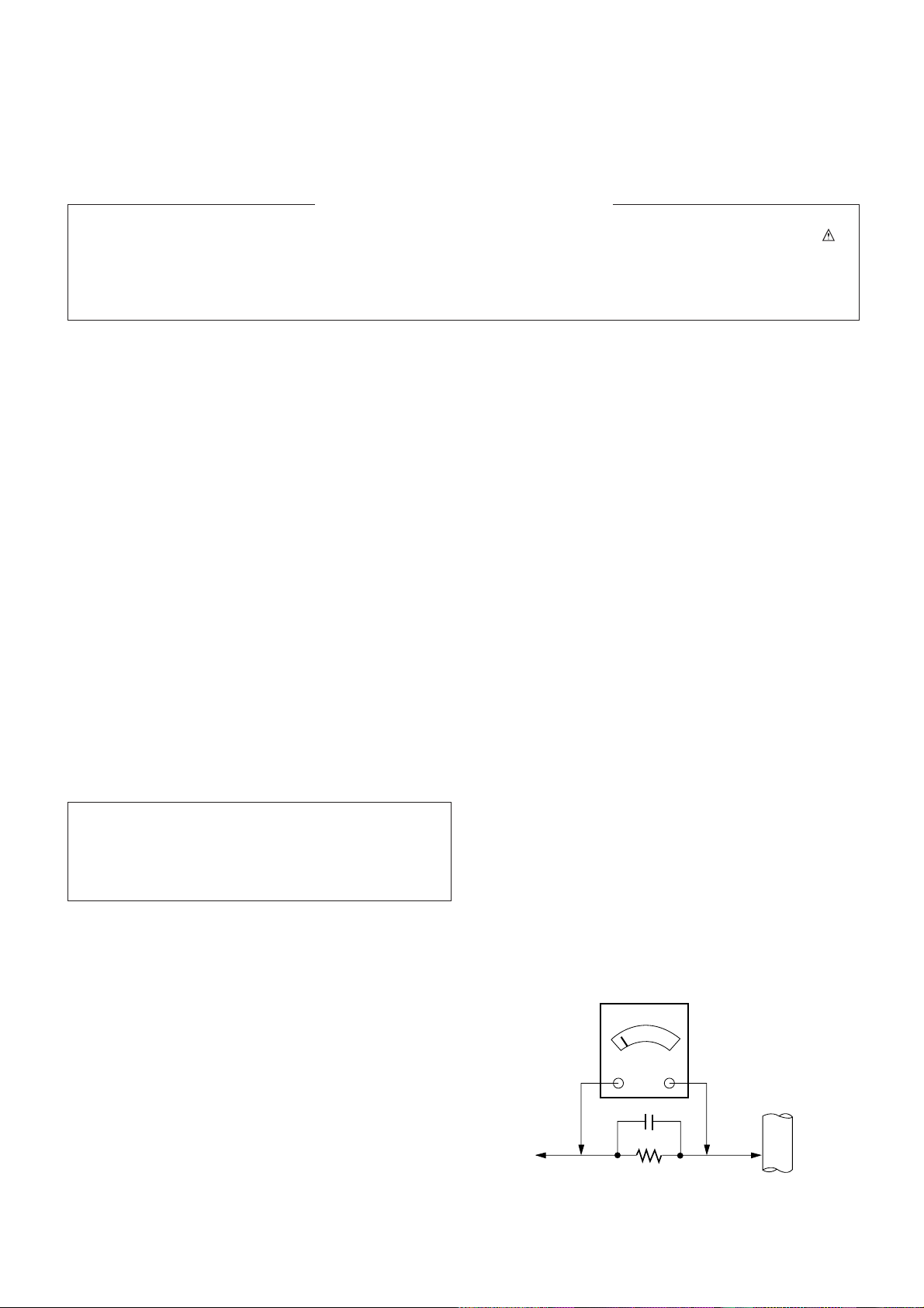
Leakage Current Hot Check (See below Figure)
Plug the AC cord directly into the AC outlet.
Do not use a line Isolation Transformer during this check.
Connect 1.5K/10watt resistor in parallel with a 0.15uF capacitor
between a known good earth ground (Water Pipe, Conduit, etc.)
and the exposed metallic parts.
Measure the AC voltage across the resistor using AC
voltmeter with 1000 ohms/volt or more sensitivity.
Reverse plug the AC cord into the AC outlet and repeat AC
voltage measurements for each exposed metallic part. Any
voltage measured must not exceed 0.75 volt RMS which is
corresponds to 0.5mA.
In case any measurement is out of the limits specified, there is
possibility of shock hazard and the set must be checked and
repaired before it is returned to the customer.
Leakage Current Hot Check circuit
The source of X-RAY RADIATION in this TV receiver is the
High Voltage Section and the Picture Tube.
For continued X-RAY RADIATION protection, the
replacement tube must be the same type tube as specified in
the Replacement Parts List.
1.5 Kohm/10W
To Instrument's
exposed
METALLIC PARTS
Good Earth Ground
such as WATER PIPE,
CONDUIT etc.
AC Volt-meter
IMPORTANT SAFETY NOTICE
0.15uF
Page 4

- 4 -
CAUTION: Before servicing receivers covered by this service
manual and its supplements and addenda, read and follow the
SAFETY PRECAUTIONS
on page 3 of this publication.
NOTE:
If unforeseen circumstances create conflict between the
following servicing precautions and any of the safety
precautions on page 3 of this publication, always follow the
safety precautions. Remember: Safety First.
General Servicing Precautions
1. Always unplug the receiver AC power cord from the AC
power source before;
a. Removing or reinstalling any component, circuit board
module or any other receiver assembly.
b. Disconnecting or reconnecting any receiver electrical plug
or other electrical connection.
c.
Connecting a test substitute in parallel with an electrolytic
capacitor in the receiver.
CAUTION: A wrong part substitution or incorrect
polarity installation of electrolytic capacitors may result
in an explosion hazard.
d. Discharging the picture tube anode.
2. Test high voltage only by measuring it with an appropriate
high voltage meter or other voltage measuring device (DVM,
FETVOM, etc) equipped with a suitable high voltage probe.
Do not test high voltage by "drawing an arc".
3. Discharge the picture tube anode only by (a) first connecting
one end of an insulated clip lead to the degaussing or kine
aquadag grounding system shield at the point where the
picture tube socket ground lead is connected, and then (b)
touch the other end of the insulated clip lead to the picture
tube anode button, using an insulating handle to avoid
personal contact with high voltage.
4. Do not spray chemicals on or near this receiver or any of its
assemblies.
5. Unless specified otherwise in this service manual, clean
electrical contacts only by applying the following mixture to
the contacts with a pipe cleaner, cotton-tipped stick or
comparable nonabrasive applicator; 10% (by volume)
Acetone and 90% (by volume) isopropyl alcohol (90%-99%
strength)
CAUTION: This is a flammable mixture.
Unless specified otherwise in this service manual, lubrication
of contacts in not required.
6. Do not defeat any plug/socket B+ voltage interlocks with
which receivers covered by this service manual might be
equipped.
7. Do not apply AC power to this instrument and/or any of its
electrical assemblies unless all solid-state device heat sinks
are correctly installed.
8. Always connect the test receiver ground lead to the
receiver chassis ground before connecting the test receiver
positive lead.
Always remove the test receiver ground lead last.
9.
Use with this receiver only the test fixtures specified in this
service manual.
CAUTION: Do not connect the test fixture ground strap to
any heatsink in this receiver.
Electrostatically Sensitive (ES) Devices
Some semiconductor (solid state) devices can be damaged
easily by static electricity. Such components commonly are
called
Electrostatically Sensitive (ES) Devices.
Examples of
typical ES devices are integrated circuits and some fieldeffect
transistors and semiconductor "chip" components. The
following techniques should be used to help reduce the
incidence of component damage caused by static by static
electricity.
1. Immediately before handling any semiconductor component
or semiconductor-equipped assembly, drain off any
electrostatic charge on your body by touching a known earth
ground. Alternatively, obtain and wear a commercially
available discharging wrist strap device, which should be
removed to prevent potential shock reasons prior to
applying power to the unit under test.
2. After removing an electrical assembly equipped with ES
devices, place the assembly on a conductive surface such as
aluminum foil, to prevent electrostatic charge buildup or
exposure of the assembly.
3. Use only a grounded-tip soldering iron to solder or unsolder
ES devices.
4. Use only an anti-static type solder removal device. Some
solder removal devices not classified as "anti-static" can
generate electrical charges sufficient to damage ES devices.
5. Do not use freon-propelled chemicals. These can generate
electrical charges sufficient to damage ES devices.
6. Do not remove a replacement ES device from its protective
package until immediately before you are ready to install it.
(Most replacement ES devices are packaged with leads
electrically shorted together by conductive foam, aluminum
foil or comparable conductive material).
7. Immediately before removing the protective material from
the ieads of a replacement ES device, touch the protective
material to the chassis or circuit assembly into which the
device will be installed.
CAUTION:Be sure no power is applied to the chassis or
circuit, and observe all other safety precautions.
8. Minimize bodily motions when handling unpackaged
replacement ES devices. (Otherwise harmless motion such
as the brushing together of your clothes fabric or the lifting
of your foot from a carpeted floor can generate static
electricity sufficient to damage an ES device.)
General Soldering Guidelines
1. Use a grounded-tip, low-wattage soldering iron and
appropriate tip size and shape that will maintain tip
temperature within the range or 500¡£F to 600¡£F.
2. Use an appropriate gauge of RMA resin-core solder
composed of 60 parts tin/40 parts lead.
3. Keep the soldering iron tip clean and well tinned.
4. Thorohly clean the surfaces to be soldered. Use a mall
wirebristle (0.5 inch, or 1.25cm) brush with a metal handle.
Do not use freon-propelled spray-on cleaners.
5. Use the following unsoldering technique
a. Allow the soldering iron tip to reach normal temperature.
(500¡£F to 600¡£F)
b. Heat the component lead until the solder melts.
c. Quickly draw the melted solder with an anti-static,
suction-type solder removal device or with solder braid.
CAUTION: Work quickly to avoid overheating the circuit
board printed foil.
6. Use the following soldering technique.
a. Allow the soldering iron tip to reach a normal
temperature (500¡£F to 600¡£F)
b. First, hold the soldering iron tip and solder the strand
against the component lead until the solder melts.
SERVICING PRECAUTIONS
Page 5

- 5 -
c. Quickly move the soldering iron tip to the junction of the
component lead and the printed circuit foil, and hold it
there only until the solder flows onto and around both the
component lead and the foil.
CAUTION: Work quickly to avoid overheating the circuit
board printed foil.
d. Closely inspect the solder area and remove any excess
or splashed solder with a small wire-bristle brush.
IC Remove/Replacement
Some chassis circuit boards have slotted holes (oblong) through
which the IC leads are inserted and then bent flat against the
circuit foil. When holes are the slotted type, the following
technique should be used to remove and replace the IC. When
working with boards using the familiar round hole, use the
standard technique as outlined in paragraphs 5 and 6 above.
Removal
1. Desolder and straighten each IC lead in one operation by
gently prying up on the lead with the soldering iron tip as the
solder melts.
2. Draw away the melted solder with an anti-static suctiontype solder removal device (or with solder braid) before
removing the IC.
Replacement
1. Carefully insert the replacement IC in the circuit board.
2. Carefully bend each IC lead against the circuit foil pad and
solder it.
3. Clean the soldered areas with a small wire-bristle brush.
(It is not necessary to reapply acrylic coating to the areas).
"Small-Signal" Discrete Transistor
Removal/Replacement
1. Remove the defective transistor by clipping its leads as
close as possible to the component body.
2. Bend into a "U" shape the end of each of three leads
remaining on the circuit board.
3. Bend into a "U" shape the replacement transistor leads.
4. Connect the replacement transistor leads to the
corresponding leads extending from the circuit board and
crimp the "U" with long nose pliers to insure metal to metal
contact then solder each connection.
Power Output, Transistor Device
Removal/Replacement
1. Heat and remove all solder from around the transistor leads.
2. Remove the heatsink mounting screw (if so equipped).
3. Carefully remove the transistor from the heat sink of the
circuit board.
4. Insert new transistor in the circuit board.
5. Solder each transistor lead, and clip off excess lead.
6. Replace heatsink.
Diode Removal/Replacement
1. Remove defective diode by clipping its leads as close as
possible to diode body.
2. Bend the two remaining leads perpendicular y to the circuit
board.
3. Observing diode polarity, wrap each lead of the new diode
around the corresponding lead on the circuit board.
4. Securely crimp each connection and solder it.
5. Inspect (on the circuit board copper side) the solder joints of
the two "original" leads. If they are not shiny, reheat them
and if necessary, apply additional solder.
Fuse and Conventional Resistor
Removal/Replacement
1. Clip each fuse or resistor lead at top of the circuit board
hollow stake.
2. Securely crimp the leads of replacement component around
notch at stake top.
3. Solder the connections.
CAUTION: Maintain original spacing between the replaced
component and adjacent components and the circuit board
to prevent excessive component temperatures.
Circuit Board Foil Repair
Excessive heat applied to the copper foil of any printed circuit
board will weaken the adhesive that bonds the foil to the circuit
board causing the foil to separate from or "lift-off" the board.
The following guidelines and procedures should be followed
whenever this condition is encountered.
At IC Connections
To repair a defective copper pattern at IC connections use the
following procedure to install a jumper wire on the copper
pattern side of the circuit board. (Use this technique only on IC
connections).
1. Carefully remove the damaged copper pattern with a sharp
knife. (Remove only as much copper as absolutely
necessary).
2. carefully scratch away the solder resist and acrylic coating
(if used) from the end of the remaining copper pattern.
3. Bend a small "U" in one end of a small gauge jumper wire and
carefully crimp it around the IC pin. Solder the IC connection.
4. Route the jumper wire along the path of the out-away
copper pattern and let it overlap the previously scraped end
of the good copper pattern. Solder the overlapped area and
clip off any excess jumper wire.
At Other Connections
Use the following technique to repair the defective copper
pattern at connections other than IC Pins. This technique
involves the installation of a jumper wire on the component
side of the circuit board.
1. Remove the defective copper pattern with a sharp knife.
Remove at least 1/4 inch of copper, to ensure that a
hazardous condition will not exist if the jumper wire opens.
2. Trace along the copper pattern from both sides of the
pattern break and locate the nearest component that is
directly connected to the affected copper pattern.
3. Connect insulated 20-gauge jumper wire from the lead of
the nearest component on one side of the pattern break to
the lead of the nearest component on the other side.
Carefully crimp and solder the connections.
CAUTION: Be sure the insulated jumper wire is dressed so
the it does not touch components or sharp edges.
Page 6
- 6 -
SPECIFICATIONS
NOTE : Specifications and others are subject to change without notice for improvement.
A Scope
This specification can be applied to all the Projection television related to MP-03AB Chassis.
A Test Condition
Conduct the test as mentioned below.
1) Temperature : 25¡ 5
°C
2) Relative Humidity : 65¡ 10%
3) Power Voltage : Standard input voltage (230V~, 50Hz)
But Standard input voltage mark value is marked by model.
4) Use the parts only designated in B.O.M.,PARTS SPEC.,or drawings.
5) Follow each drawing or spec for spec and performance of parts,based upon P/N of RPL
6)
Warm up TV set for more than 60min before the
measurement.
A Test and Inspection Method
1) Performance : Follow the Standard of LG TV test
2) Extra requirement
Chassis
MP-03AB
RE-39NZ43RB
RE-44/49/54NA13RB
RE-44NA14T
RE-40/45/56NZ60RB
RE-44/49/56NZ23RB
RT-39NZ43RB
RT-44/49/54NA13RB/RP
RT-44/49/54NA23RB/RP
RT-44/49/54NA43RB/RP
RT-44NA14T
RT-40/45/56NZ60RB/RP
RT-44/49/56NZ23RB/RP
RL-39NZ43RB
RL-44/49/54NA13RB
RL-44NA14T
RL-40/45/56NZ60RB
RL-44/49/56NZ23RB
Europe (except France)
China, Asia, Africa, Middle
East
France
LG ‘T’/ ‘RB’ : Teletext option
Model Name Market Place Brand Remark
Model
RE/RL-44NA14T
RE/RL-40NZ60RB
Market
EUROPE
Remark
SAFETY : CB
CE EMI : EN55013
EMS : EN55020
Appliance
OK
Page 7
- 7 -
A Test and Inspection Method
Item
Receiving System
Available Channel
Input Voltage
Market
Screen Size
Aspect Ratio
Tuning System
TUNER IF
Operating Environment
Storage Environment
No
1
2
3
4
5
6
7
8
9
10
Remark
AV can be input NTSC-M
S (RL model for France)
S (RT model w/o China)
S (RE,RL, China model)
S (With Teletext model)
S (W/O Teletext model)
Specification
PAL, SECAM-BG
PAL, SECAM-DK, PAL-I
PAL, SECAM-BG
SECAM-LL’
PAL, SECAM-BG,
PAL, SECAM-DK, PAL-I
NTSC-M
1) VHF : E2 ~ E12
2) UHF : E21 ~ E69
3) CATV : S1~S20
4) HYPER : S21~S41
LL’VHF : B,C,D
AC 110-240V~, 50/60Hz
AC 230V~, 50/60Hz
Europe except France
France
Asia, Africa, Middle East
44/49/54, 39/40/45/50/57 inch
4:3, 16:9
FVS 100 Program
FVS 200 Program
38.9MHz, 39MHz
1)Temperature : -5 ~ 40 °C
2) Humidity : 30 ~ 95 %
3) Temperature :-20 ~ 50 °C
4) Humidity : 30 ~ 95 %
RE
RL
RT
(S Mark : Option Item)
RE
RL
RT
Page 8

A Feature and Function
- 8 -
Item
Feature AV Input
AV Output
Component Input
S-Video Input
SCART
key Local Key
Remocon
Picture PSM
User Control
DRPC
VM
Convergence
Sound SSM
AVL
DBS
TV Speaker
Balance
Timer Clock
Off time
On time
Auto sleep
Special Language
Input
PIP Input
child lock
Etc. Convergence
Comb Filter
SVM
ARC
ACMS
Auto Off
Teletext
No
1
2
3
4
5
6
7
Remark
Side
S (Rear, RT model)
S (Rear, RT model)
Rear 480i/ 480P/ 576i
(1080i for CHINA)
side 1, Rear 1
S (Rear, RE,RL model)
Front
S INDEX (With Index)
Tint : NTSC system only
S
S 3*3 EDC
S Dolby virtual (Option)
S
S S-VIDEO4 (EU ONLY)
S S-VIDEO4 (EU ONLY)
S
S
S
S
Specification
1 V/L/R
2 V/L/R
1 V/L/R
2 COMPONENT1, L/R
COMPONENT2, L/R
2 Y/C
3 Full SCART (with RGB Input) : 1
Half SCART : 1 (AV In/Out)
Half SCART ; 1 (AV In, YC In)
POWER, MENU, VOL(
F,G), PR(D,E)
TV/AV, OK, MUTE (W/O Index)
NEC Code
Dynamic/ Standard/ Mild/ Game/ User
Contrast/ Brightness/ Colour/ Sharpness/ Tint
On/ Off
1/ 2/ 3/ 4
1[+] Point/ 9[+] Point
Auto Convergence (option)
Dolby Virtual/ Flat/ Music/ Movie/ Speech/ User
On/ Off
On/ Off
On/ Off
L 50 ~ 0 ~ R 50
-- : -- AM
-- : -- AM Off (On)
-- : -- AM Pr 1 VOL 30 Off(On)
On/ Off
Multi language
TV/ AV1/ AV2/ AV3/ AV4/ S-VIDEO4/
Component1/ Component2
TV/ AV1/ AV2/ AV3/ AV4/ S-VIDEO4
On/ Off
MANUAL ADJUST
Auto Adjust
Digital comb filter
O
4:3/ 16:9 (4:3 Model)
16:9/ 14:9/ ZOOM/ AUTO/ 4:3 (16:9 Model)
O
On/ Off
TOP/ FLOF/ LIST
Page 9
- 9 -
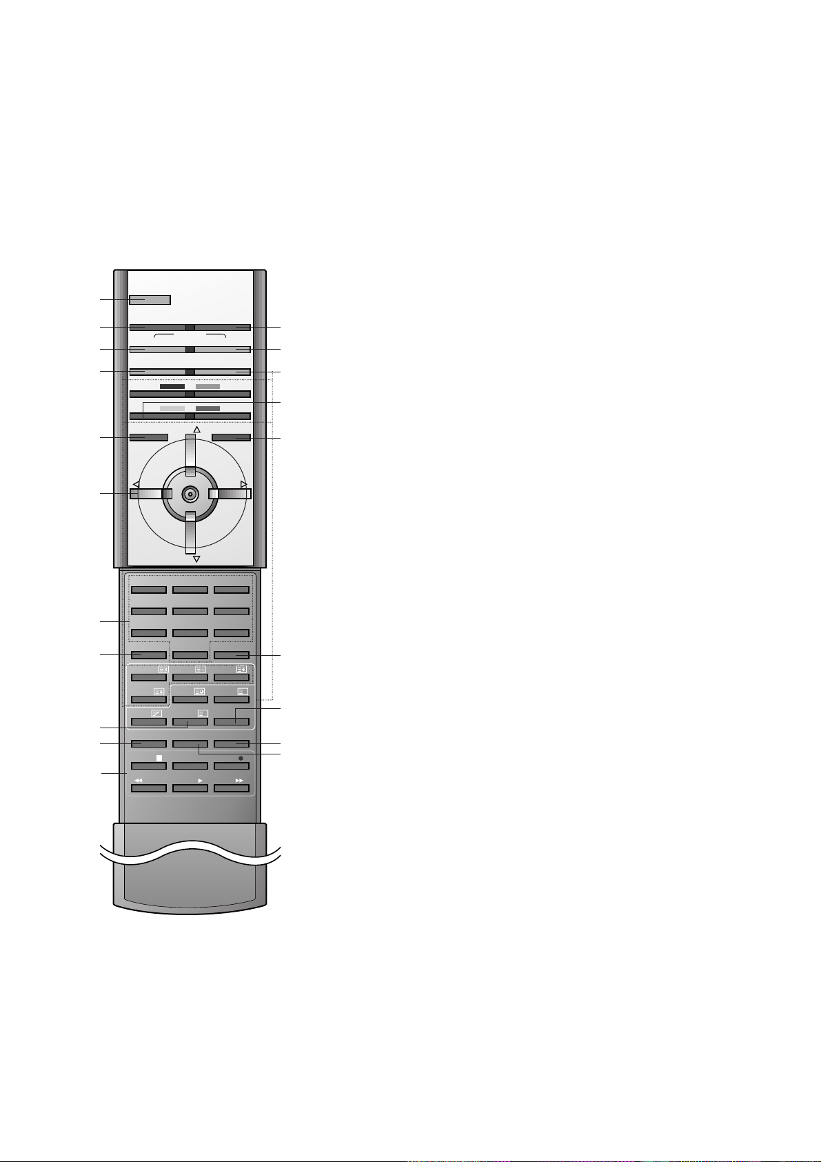
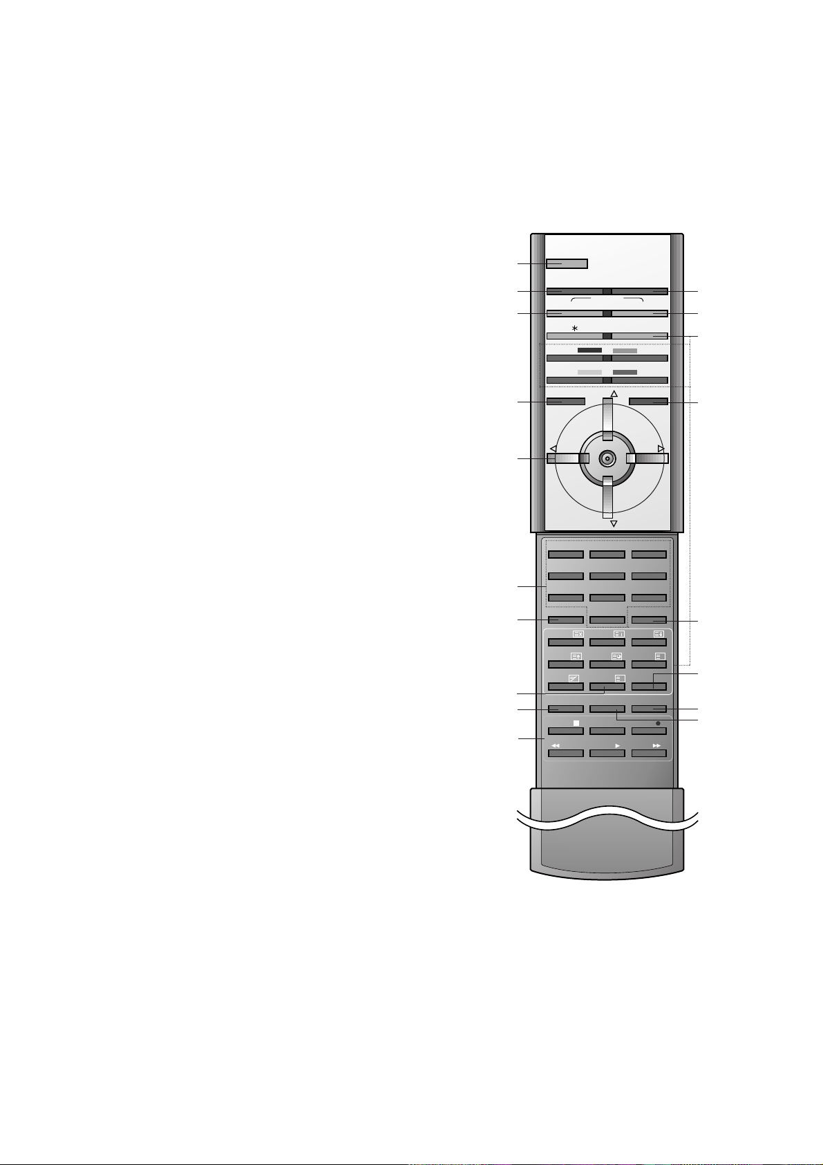
CONTROLS DESCRIPTION
All the functions can be controlled with the remote control handset.
Some functions can also be adjusted with the buttons on the front
panel of the set.
Remote control handset
Before you use the remote control handset, please install the batteries. See the next page.
1. POWER
switches the set on from standby or off to standby.
2. TV/AV
selects TV or AV mode.
switches the set on from standby.
3. TURBO SOUND BUTTON
selects Turbo sound.
4. PIP BUTTONS (option)
PIP
switches the sub picture on or off.
PR +/-
selects a programme for the sub picture.
SWAP
alternates between main and sub picture.
INPUT
selects the input mode for the sub picture.
SIZE
adjusts the sub picture size.
STILL
freezes motion of the sub picture.
POSITION
relocates the sub picture in clockwise direction.
SCAN
switches on or off the programme scan mode 12 sub pictures.
5. MENU
selects a menu.
6.
D / E
(Programme Up/Down)
selects a programme or a menu item.
switches the set on from standby.
F / G
(Volume Up/Down)
adjusts the volume.
adjusts menu settings.
OK
accepts your selection or displays the current mode.
7. NUMBER BUTTONS
switches the set on from standby or directly select a number.
8. PSM (Picture Status Memory)
recalls your preferred picture setting.
9. SLEEP
sets the sleep timer.
10. I/II
selects the language during dual language broadcast.
selects the sound output (option).
11. VCR BUTTONS
control a LG video cassette recorder.
123
456
7
PSM SSM
8
0
POSITION
STILL
SCAN
MIX
REVEAL
?
M
TIME
SIZE
LIST
SLEEP
I/II ARC
Q.VIEW
STOP REC
P/STILL
REW FF
PLAY
9
POWER
TV/AV MULTIMEDIA
SOUND PICTURE
TURBO
PIP TEXT
PR
- PR +
INPUTSWAP
MENU PR
VOL
OK
VOL
PR
MUTE
1
12
13
14
16
17
18
19
20
15
2
3
4
5
6
7
8
10
9
11
(With TELETEXT/PIP)
Page 10
- 10 -
12. MULTIMEDIA
selects Component 1 or Component 2 modes.
switches the set on from standby.
13. TURBO PICTURE BUTTON
selects Turbo picture.
14. TELETEXT BUTTONS (option)
These buttons are used for teletext.
For further details, see the ‘Teletext’ section.
15. SWAP
returns to the previously viewed programme.
selects a favourite programme.
16. MUTE
switches the sound on or off.
17. SSM (Sound Status Memory)
recalls your preferred sound setting.
18. LIST
displays the programme table.
19.
ARC (Aspect Ratio Control)
select your desired picture format.
20. Q.VIEW
returns to the previously viewed programme.
selects a favourite programme.
*
: No function
COLOURED BUTTONS : These buttons are used for teletext (only
TELETEXT models) or programme edit.
Note : In teletext mode, the PR +/-, SWAP and INPUT buttons are
used for teletext function.
1 2 3
4 5 6
7
PSM SSM
8
0
UPDATE
HOLD
INDEX
MIX
REVEAL
?
M
TIME
SIZE
LIST
SLEEP
I/II ARC
Q.VIEW
STOP REC
P/STILL
REW FF
PLAY
9
POWER
TV/AV MULTIMEDIA
SOUND PICTURE
TURBO
TEXT
MENU PR
VOL
OK
VOL
PR
MUTE
1
12
13
14
16
17
18
19
20
2
3
5
6
7
8
10
11
(With TELETEXT/Without PIP)
9
Page 11
- 11 -
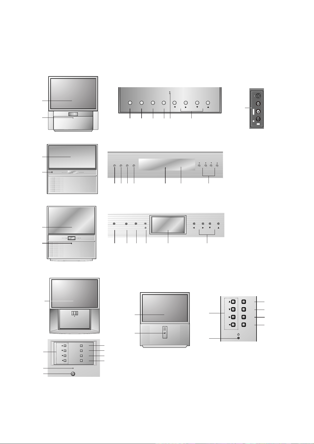
S-VIDEO VIDEO
L/MONO RAUDIO
AV3
11
Front panel
ON/OFF
PR
MENU MUTE
TV/AV
VOL
OK
PR
MENU MUTE
TV/AV
VOL
OK
8
1
•
RE/RL-44/49/54NA13/14 series
7
6
5
4
23
•
RE/RL-44/54NA23/24 series
TV/AV OK INDEX VOL PRMENU
8
1
•
RE/RL-39NZ43 series
TV/AV OK INDEX
VOL PR
MENU
7 6 5 9 3 10 2
TV/AV
MENU
OK
VOL
PR
TV/AV MENU
VOL PR
OK
8
716 5 3 10 2
•
RE/RL-44/49/54NZ23 series
ON/OFF
PR
PR
VOL
VOL
MUTE
MENU
OK
TV/AV
2
4
6
5
7
ON/OFF
PR
PR
VOL
VOL
MUTE
MENU
OK
TV/AV
8
1
3
•
RE/RL-44/54NA43/44 series
PR
PR
VOL
VOL
POWER
MUTE
MENU
OK
TV/AV
8
1
PR
PR
VOL
VOL
MUTE
MENU
OK
TV/AV
2
3
4
6
5
7
(Side panel)
Page 12
- 12 -
1. MAIN POWER (ON/OFF)
switches the set on or off.
2.
FF / GG
(Volume Up/Down)
adjusts the volume.
adjusts menu settings.
DD / EE
(Programme Up/Down)
selects a programme or a menu item.
switches the set on from standby.
3. POWER/STANDBY INDICATOR
illuminates brightly when the set is in standby
mode.
dims when the set is switched on.
4. MUTE (option)
switches the sound on or off.
5. OK
accepts your selection or displays the current
mode.
6. MENU
selects a menu.
7. TV/AV
selects TV or AV mode.
switches the set on from standby.
8. REMOTE CONTROL SENSOR
9. INDEX (option)
switches LED DISPLAY on or off.
10. LED (Light Emitting Diode) DISPLAY
(option)
illuminates brightly when the set is switched
on.
Option : Only RE/RL-39NZ43 series,
: PAL/SECAM indicator
: NTSC indicator
: STEREO indicator
: SLEEP Timer indicator
: CHILD LOCK indicator
11. AUDIO/VIDEO IN SOCKETS (AV3)
Connect the audio/video out sockets of external equipment to these sockets.
S-VIDEO/AUDIO IN SOCKETS (S-AV)
Connect the video out socket of an S-VIDEO
VCR to the S-VIDEO socket.
Connect the audio out sockets of the SVIDEO VCR to the audio sockets as in AV3.
*
CASTERS (on the bottom)
turn and move the set easily.
Front panel
S-VIDEO VIDEO
L/MONO AUDIO
AV3
R
(Side panel)
11
PR
MENU
MUTE
TV/AV
VOL
OK
8
1
•
RE/RL-39/45/56NZ60 series
PR
MENU MUTE
TV/AV
VOL
OK
7 6 5 4 3 2
STEREO
SLEEP
LOCK
Page 13
- 13 -
These instructions are applied to only MP-03AB chassis.
Notes
1.Because this is not a hot chassis, it is not necessary to use an
isolation transformer.
However, the use of isolation transformer will help protect
test instrument.
2.Adjustment must be done in the correct order.
3.The receiver must be operated for about 60 minutes prior to
the adjustment.
Pre-heatrun must be operated receiving moving pictures or
100% white pattern.
[ Never operate the SET over 10 minutes with still picture
because a fluorescent material may get damage.
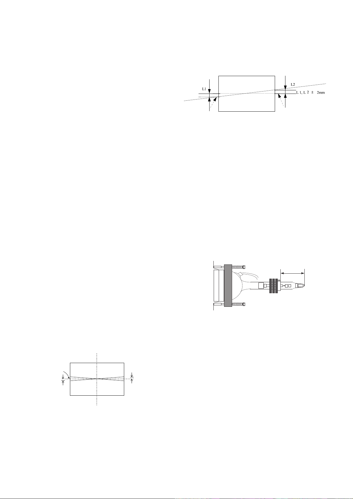
O Raster Slope/Focus 1th Adjustment
1. Preliminary steps
1) Apply power to the unit and switch the unit ON.
2) Receive the EU 05 CH signal.
3) Select INSTART key on the Remote Control and then select
“0 RASTER ADJ” move the cursor or by pressing the key
No. 0.
4) Adjust Lens Focus/Electric focus temporarily.
[ When select “0 RASTER ADJ” mode after entering adjustment
mode with INSTART key, the convergence reset and then
preparation for adjustment complete.
[ The convergence reset is possible even from convergence
adjustment mode.
1) Enter into convergence adjustment mode: Select INSTART
key on the Remote Control and then select “3
CONVERGENCE” move the cursor or using the key No..
2) Convergence reset: After press the key No. 5, press the
ENTER key.
3) Adjustment mode release: Press the INSTART key
2. Adjustment
1) Display only the Green raster using lens covers to block Red
and Blue.
2) Rotate the Green DY and tilt the screen like the figure below.
3) Make 2color raster with Red or Blue and Green.
4) Coincide the slope of red and blue raster to that of green.
Note) 1. When adjusting raster slope, loosen the DY and fasten it
after adjusting.
2. Never rotate and adjust the fixed DY without loosing it.
O Beam Alignment Adjustment
1. Test Equipment
Video Test Generator(801GF) or Signal Generator can produce
NTSC DOT pattern(408NPS or 5518/5418 equipment)
2. Preparation
1) Heat run over 60 minutes.
2) Pre-adjust Raster slope,Raster position & Lens focus &
centering Magnet.
3) Check if the Magnet is located 45mm from the end of CRT.
4) In case of using 801GF : Receive #13 DOT Pattern of VGA
mode(Format #5) through PC input terminal.
In case of using NTSC generator : Receive Dot signal
through the external input terminal.
3. 2-Pole Magnet Adjustment
1) Make Green raster using lens cover.
2) Check the center position of DOT pattern on the center of the
screen after turning Green focus volume left.
3) Turning green focus volume right and adjust 2-Pole magnet
so the position to coincide that of item ”(2)”.
4) Adjust not to shift the screen by turning green focus volume
clockwise and counter clockwise.
5) If the screen shifts, readjust (2)~(4).
6) Do the same method in Red and Blue.
4. Beam Shape (4 & 6-Pole Magnet) Adjustment
1) Do after 2-Pole magnet adjustment.
2) Make Green raster using lens cover and turn the focus
volume right.
3) Make the dot in the center a perfect circle using 4 & 6-Pole
magnet.
4) Do the same method in Red & Blue.
5) Fasten the Magnet after adjustment.
6) Adjust focus accurately.
ADJUSTMENT INSTRUCTIONS
L
L
Mechanical
center
L ¡´!2mm
Red/Blue Light
Green Light
45mm
Page 14

O Centering Magnet Adjustment
1. Preliminary steps
1) Receive the EU 05 CH signal.(PR.1 : PAL B/G 175.25MHZ)
2)
Press the keys of Remote Controller for adjustment to reset the
convergence.
a.Adjustment mode:Press the IN-START key.
b.Data reset : Press 0 KEY.
c.Adjustment mode cancellation : Press the
ENTER
key.
2. Adjustment
1) Operate adjustment about Red,Green,Blue centering
magnet.
2) SGS-THOMSON Convergence assy
Adjust until the center of blue signal is shifted up to 40mm
left from that of green signal and center of red signal is
shifted up to 40mm right from that of green signal with
turning the centering magnet.
3) After adjustment, re-adjust convergence data and exit the
adjusting mode.
a.Adjustment mode:Press the IN_START key.
b.Data reset : Press 0 KEY.
c.Adjustment mode cancellation : Press the Enter key.
O High Voltage Regulation Adjustment
1. Test Equipment
Digital Multi-Meter(DMM)
2. Preparation for Adjustment.
Select picture mode to ‘DYNAMIC’ in no signal input.
3. Adjustment
1) Press the IN_START key and then press ‘1’ key.(HV ADS)
2) Connect “+” terminal(Red) of DMM to the P415 of the
Deflection PCB, [+] and the “-”terminal(Black) to the P416,[-].
3) Adjust VR401 so that the voltage of multimeter to be below
voltage.
Voltage : 21.7 ! 0.1V.
4) Exit the adjustment mode by pressing the enter key
O CUT-OFF Voltage Adjustment
1. Preliminary steps
(1) Select INSTART key on the Remote Control and then select
“2 SCREEN ADJ” move the cursor or using the key No..
(2) Adjustment must be operated in a dark room (simple dark
room)
2. Adjustment
1) Test Equipment: Oscilloscope, 100:1 Probe
2) Connect oscilloscope to cathode of R, G, B(R926R/B/G:
SCREEN ADJ on the PCB) and GND.
3) Turning Screen Volume (R/G/B) in Focus Pack and adjust
R/G/B is 165V!0.5V.
4) After adjustment complete, exit the RASTER adjustment
mode using ENTER key and exit the SVC adjustment mode
using INSTART key.
O Deflection Adjustment
1. Preliminary steps
1) NTSC mode should be adjusted after adjusting PAL mode.
2) PAL adjustment should be done in the EU CH05,and NTSC
adjustment should be done in the CH13 or Multi 48CH.
Note, RE/RL Model(without NTSC-M system) receive CH13
in the V-3 input.
3) Press the button of Remote Controller for adjustment to reset
the convergence
Adjustment Mode : Press the IN_START key
Data reset : Press the 0 key.
Saving and returning Adjustment mode : Press the ENTER
Key
Note. Refer adjustment items to Appendix1.
2. PAL Mode Deflection adjustment
Do not adjust H-POS,V-POS, V-LIN, S-COR, A-BOW, A-ANG,
UCPIN, LCPIN, V-ASP,V-SCR in PAL mode.
Select the below each mode using CH
D, E and adjust using
VOL
F, G on the remote controller.
At SVC mode, press the ‘0’ key get into the deflection
adjustment mode.
1) H-POS (Horizontal Position Adjustment)
Adjust so that the horizontal center line of screen is in accord
with the geometric horizontal center line of screen JIG.
2) V-POS (Vertical Position Adjustment)
Adjust so that the vertical center line of picture is in accord
with the vertical center line of the screen.
3) HSIZE (Horizontal SIZE Adjustment)
Adjust so that the outermost left and right vertical line of the
screen is accord with the last point of the frame
4) VSIZE (Vertical SIZE Adjustment)
Adjust until Sixth vertical center line from upper and lower
center of the picture is accord with the last point of the frame.
5) U-VL (Upper Vertical Linearity Adjustment)
Adjust
the vertical interval of screen upper.
6) L-VL (Lower Vertical Linearity Adjustment)
Adjust
the vertical interval of screen lower.
- 14 -
0V
165V±0.5V
Vertical period
2 Pole Magnet
4 Pole Magnet
6 Pole Magnet
Page 15
7) PIN-P (Horizontal Trapezoid Distortion Compensation
Adjustment)
Adjust to make the length of top horizontal line same with it of
the bottom horizontal line.
8) PIN-A (Horizontal PIN Distortion Compensation Amount
Adjustment)
Adjust the horizontal width of picture upper and lower is to be
same.
9) V-LIN (Vertical Linearity Adjustment)
Adjust vertical size of the picture to be same with upper and
lower.
10) S-COR (Vertical S Correction)
Adjust so that all distance between each horizontal lines are to
be the same.
11) A-BOW (AFC BOW)
Adjust so that the vertical line at every 4 corners of the screen
look like parallel with the vertical center lines of picture.
12) A-ANG (AFC Angle)
Adjust so that all vertical slope of the picture are vertical.
13) UCPIN (Upper Corner Pincushion)
The pin cushion adjustment of upper part
14) LCPIN (Lower Corner Pincushion)
The pin cushion adjustment of lower part
15) V-ASP(Vertical Aspect Ratio)
Adjust the vertical aspect ratio.
16) V-SCR (Vertical Scroll)
Adjust the vertical aspect position.
Store the adjusted data in EEPROM by pressing the ENTER key
before exiting adjustment mode.
Exit the adjustment mode by pressing the ENTER key.
3. NTSC Mode Deflection Adjustment
Do not adjust V-LIN, S-COR, A-BOW, A-ANG, UCPIN, LCPIN,
V-ASP, V-SCR in NTSC mode.
1) Adjust vertical size (V-SIZE Adjustment) until fifth vertical bar
from upper and lower center screen is accord with the edge
of the frame.
2) Adjust horizontal size (H-SIZE Adjustment) until third bar to
indicate horizontal size of circle is accord with the edge of
the frame.
3) Do other adjustments the same as in PAL mode.
4. 1080i Mode deflection Adjustment (option)
(1) Test Equipment
SETTOP BOX with 1080i output or MSPG-925LTH
(Programmael VIDEO Singnal Generator).
(2) Preliminary steps
1) After adjust 1080i with output of the SETTOP BOX,
connects to AV-3 (Side-AV) the Y signal only which is
output from SETTOP BOX with the VIDEO input terminal.
2) Select INSTART key on the Remote Control and then
select “5 1080I-ADJ” move the cursor or using the key
No.5.
3) Adjust vertical size (V-SIZE Adjustment) until fifth vertical
bar from upper and lower center screen is accord with the
edge of the frame.
4) Adjust horizontal size (H-SIZE Adjustment) until twelfth
vertical bar is accord with the edge of th frame.
5) Do other adjustments the same as in PAL mode
O
Lens Focus & Electronic Focus Adjustment
1. Preliminary steps
1) Electronic focus,Raster slope & Raster position must be preadjusted.
2) Heat-run over 60 minutes.
- 15 -
Third bar
Fifth vertical BAR
Sixth Vertical Line
<Fig. 3>
Page 16
3) Receive Crosshatch pattern.
(PAL:EU07(PR 8) or NTSC:09CH(PR 13))
* Note: Loosen the butterfly nut in the lens tub slightly,being
careful that it is mot loosened to the point that the lens can
move out of focus.
4) Adjustment must be done in a dark room(simple dark room)
Be careful not to touch the lens during adjustment.
5) Make any one color raster using lens covers.
6) Rotating lens right from the front side chromatic haze occurs
beside Cross-hatch line changes as follows;
2. G-lens Adjustment
1) Rotate the lens until the chromatic haze changes from blue to
red.
2)
Viewing the all screen, in no case of the chromatic aberration
appeared slimly within 3.5 cross-Hatch of the picture center. At
this time, in case that the red chromatic aberrations bright line
isn't equal, adjust Green lens so that the red chromatic
aberration is appeared more than previous time.
3) Switching the signal to 13CH and operate adjustment
minutely.
4) Adjust Green focus control volume of focus pack so that the
external big circle's part appeared clearly.
5) Adjust accurately by repeat the upper control.
6) Especially, noting to the Green light because it influenced on
picture’s function.
3. R-lens adjustment
1) Rotate the RED lens until the chromatic haze changes from
orange to scarlet.
2) Adjust to appear Red chromatic aberration in right 3.5 crosshatch section at center screen.Adjust the chromatic
aberration so that it located center correctly.
3) Switching the signal to 13CH and adjust it as same method of
Green lens.
4) Adjust as same method of Green lens with Red focus control
volume of focus pack.
4. B- lens adjustment
1) Rotate the lens until the chromatic aberration of 3.5 CrossHatch left from center point changes from Violet to Green.
Adjust the chromatic aberration to be center point between
violet and green.
2) Adjust as same as method of Green lens with Red focus
control volume of focus pack.
5. Focus checking
After adjustment Red,Green & Blue lens, remove lens cover
and receive Cross-Hatch pattern and check the overall focus. If
needed,repeat above.
O Convergence Adjustment
1. Preliminary steps
This adjustment should be performed after warming up 60
minutes.
1) Adjust after Horizontal/Vertical Raster position,Beam
alignment magnet, and focus adjustments have been
completed.
2) Do it always with crosshatch pattern.
3) Adjust for both PAL and NTSC system.
4) Use the JIG screen with the cross hatch pattern for
Adjustment.
2. Convergence Key
1) Convergence Mode : IN_START, ‘3’
2) Cursor shift :
F , G , D ,E
3) Cursor Movement/Adjustment Selection : ENTER
4) Cursor Color Selection : TV/AV
5) Adjustment mode out : IN_START
*Note: When cursor flashes,set is in adjustment mode When
R,G or B selected color flashes,the set is in cursor movement
mode.
O PAL Mode Adjustment
1. Preliminary steps
1) Receive the EU 05CH signal.
2) Press the buttons IN_START, ‘3’ of Remote Controller for
adjustment to get into the convergence adjustment mode.
2. Horizontal/Vertical phase adjustment
1) Press the buttons 9 & 5 to get into the phase adjustment
mode.
2) Horizontal Phase Adjustment.
Move the convex part to the quarter of vertical center by
pressing the Volume F,G key.
3) Press the ENTER Key to escape from the adjustment.
- 16 -
Lens
Red
Green
Blue
Change of chromatic aberration
Orange ¤AScarlet
Blue ¤ARed
Purple ¤AGreen
CHROMATIC
ABERRATION
CROSS HATCH
SIGNAL
Page 17
3. Pattern position adjustment
1) Change into pattern shift mode.
(Press numeric buttons “9” & “4”)
2) Make sure to overlap pattern and image.
(Use MUTE button)
3) Accord the center of image and pattern.
(Use
F , G , D ,E buttons)
4) Quit pattern shift mode. (Press “OK” button)
5) Save adjusted phase/pattern position adjustment
mode.(Press “9”, “2” & “OK” buttons)
4. Auto convergence (option)
*
Convergence is based on the auto adjustment using PC and
Camera while applying the THOMSON convergence Assy and if
need,adjust manually like below method.
5. Green convergence adjustment
1)
Show the OSD on screen by pressing 2 button,then change the
OSD to green(G) adjustment mode with pressing TV/AV button.
2) Close the cover of red PRT and blue PRT so that green
display on screen only.
3) Adjust to coincide green pattern with screen JIG pattern.
(Use
F , G , D ,E buttons)
At this time move cursor from center to around and adjust
convergence.
6. Red convergence adjustment
1)
Show the OSD on screen by pressing 2 button,then change the
OSD to red(R) adjustment mode with pressing TV/AV button.
2) If the need arises,close the cover of the blue lens.
3) Coincide the red screen with the green screen in same way
with that of green convergence adjustment.
7. Blue convergence adjustment
1)
Show the OSD on screen by pressing 2 button,then change the
OSD to blue(B) adjustment mode with pressing TV/AV button.
2) Coincide the blue screen with the green screen in same way
with that of red convergence adjustment.
8. Saving adjusted data
1) To save the data after adjustment,Press “9”, “1” & “OK”
button.
2) Quit convergence adjustment mode. (“IN_START” button)
9. NTSC mode adjustment
1) Receive the 13CH or Multi 48 CH signal.
2) Adjust as same method of PAL mode.
10. Auto-Convergence measuring or Measuring
back up data (option)
1) Operate the auto-convergence measuring or the measuring
back up data separately in PAL,NTSC mode.
2) Operate in the condition of ‘Zero magnetometer ‘ in room
after correcting convergence manually.
3) How to measuring
Press the ‘IN_START -> 3 ->MENU->3’ key to operate Auto
convergence measuring or the measuring back up data.
O White Balance Adjustment
1. Test Equipment
Brightness meter(CA110)
2. Adjustment
1) This adjustment must be operated in a dark room or
equivalent.
2) Adjust after Cut-Off and Focus adjustment.
3) The brightness meter must be located in 20¡ 5cm distance
from the center of the screen.
4) Receive WINDOW signal.
* High Light : RE/RL : 250!10
cd/m^2 (16:9)
RT : 160!10
cd/m^2 (16:9)
RE/RL : 190! 10
cd/m^2 (4:3)
RT : 160!10
cd/m^2 (4:3)
* Low Light : 10!3
cd/m^2
5) Set BRIGHT to H/Light adjustment mode in 4) and enter SVC
mode by pressing the “IN_START & 4” button. Adjust RG (R
Gain) and BG (B Gain) until color coordinate becomes
RE/RL - X=0.283 and Y=0.292, RT - X=0.269 and Y=0.274
(Deviation : !0.03).
6) Set BRIGHT to L/Light adjustment mode and adjust CR (R
Cut Off) and CB (B Cut Off) until color coordinate becomes
RE/RL - X=0.280 and Y=0.260, RT - X=0.269 and Y=0.274
(Deviation : !0.03).
7) Repeat adjusting until the color coordinate of H/Light and
L/Light is satisfied.
8) Save the data after adjustment. (Press “ENTER” button)
9) Exit adjustment mode. (“ INSTART ” button)
O Sub-Bright Adjustment
1) Tune the TV set to receive a EU 05 CH.
2) Enter WB mode by pressing the IN_START & ‘4’ button.
Adjust S-BRI data until 100% and 80% GRAY PATTERN is
classified.
(Use
F , G , D ,E, ENTER buttons)
O Auto-Convergence Check (option)
1) Check the Auto-Convergence in PAL/NTSC/1080i(option)
mode separating.
2) Press the IN_START key on R/C for adjustment and press
the CAPTION key to check whether Auto-Convergence
works normally in each mode.
3) If not,check the Convergence condition or Measuring
condition and SENSOR condition.
4)The shipment must be done after restoring the final auto
convergence data value.
* Restore a Convergence data
IN_START -> ‘3’
-> TEXT
- 17 -
Fifth Vertical Line
100% and 80% GRAY PATTERN
Page 18
- 18 -
O Check the Option Adjustment
1) Check the OPTION1~5 data of attach 6 is well recorded.
2) The option value of each suffix is started on JOB EXP of 3141VMN chassis Assy.
O Convergence Adjustment Mode
- INSTART -> 3
-> MENU
* This Mode is for engineering. So,don’t change before permission from Design Department.
0.AC POSITION READ : Distance data(After auto convergence measuring)
1.Save to 50Hz/60Hz : Save (convergence adjustment data)
It’s same 9,1,Enter.
2.Save Control data : Save (A phase adjustment data)
It’s same 9,2,OK.
3.AC Position Meas/ Meas backup data. : Execute( auto convergence measuring)
4.Pattern : Adjust location of convergence pattern.
It’s same 9,4,Enter.
5.Phase : Adjust a phase of convergence pattern.
It’s same 9,5,Enter.
6.GRID Border
7.ADJUST: Set the Dynamic focus data&auto-convergence data
HGD
HRD
VGD
BPH
BPV
29
42
44
22
35
27
55
23
20
18
Horizontal Grid Distance
Horizontal Retrace Distance
Vertical Grid Adjustment
Border Position Horizontal
Border Position Vertical
Item Description (PAL) (1080i)
27
55
38
18
26
(NTSC)
24
19
30
6
31
31
110
60
3
3
MICOM
NO
NO
29
23
31
9
31
31
110
60
3
3
MICOM
NO
NO
29
23
31
9
31
31
110
60
3
3
MICOM
NO
NO
30
27
32
13
31
31
110
60
3
3
MICOM
NO
NO
28
26
31
54
31
31
110
60
3
3
MICOM
NO
NO
30
27
32
0
31
31
110
60
3
3
MICOM
NO
NO
Item
Description
Focus parabola top value
Focus parabola middle value
Focus parabola bottom value
Focus parabola position
Start of the retrace value
Focus value during frame retrace
Force the video pattern fast blanking
Auto convergence offset
Pattern Bright Horizontal
Pattern Bright Vertical
EEPROM/MICOM selection
Initialization of AC Pattern data
Initialization of ADJ. Focus data
4:3 TV (WIDE = 0 )
PALNTSC 1080i NTSC PAL 1080i
16:9 TV (WIDE =1)
FV1
FV2
FV3
VFP
FSB
FVR
STA
ACO
PBH
PBV
OPT
ACINIT
ADJINIT
Page 19
8.OSD POSITION
9.AC PATTERN ADJ :Assign location for pattern start
O SVC Adjustment mode & Initial data
1. White Blalane adjustment data (IC:CXA2100)
2. Sound adjustment data (IC:MSP3411G)
- 19 -
8,17
10,15
11,14
11,16
13,17
13,17
9,5
10,7
10,9
17,16
17,15
18,17
14,17
14,17
15,16
18,9
18,8
19,6
H,V
H,V
4,7
3,7
3,6
6,18
5,20
4,18
H,V
10,33
12,31
13,28
14,27
15,29
15,30
12,5
13,6
13,10
14,30
14,32
15,33
11,31
11,29
12,29
15,11
15,9
16,10
H,V
H,V
5,17
3,15
3,15
6,28
5,28
4,28
H,V
<PAL mode> <NTSC mode>
• MDB(MICRONAS DYNAMIC BASS)
14
53
12
66
66
2D
19
09
OB
FC
FM
NP
SP
S1 VOL
S2 VOL
MDB-STR
MDB-HMC
MDB-HP
MDB-LP
MDB-LIM
Menu Description
FM Prescaler
NICAM Prescaler
SCART Prescaler
SCART 1 Volume
SCART 2 Volume
MDB Effect Bass Strength
MDB Harmonic Content
MDB High Pass
MDB Low Pass
MDB Amplitude Limit
Range Default
14
27
29
0D
1F
09
20
75
09
1F
2D
14
1F
13
20
75
RD
GD
BD
RC
GC
BC
S-BRI
DVCO
Menu
Description
Red Drive
Green Drive
Blue Drive
Red Cut-off
Green Cut-off
Blue Cut-off
Sub BRIGHT
Digital VCO
Range
Default
RE/RL RT
Page 20

- 20 -
03
00
00
00
03
01
02
03
02
00
01
02
03
02
0A
05
0B
07
1f
1f
07
00
00
00
02
02
03
00
00
D-COL
EXTSW
SHPFO
BLKBT
PREOV
CTILE
LTILE
PLMTL
ABLMO
CTI-M
LTI-M
GAMMA
DPIC
DC-TR
S-CON
LRGB2
P-ABL
ABLTH
CB-OF
CR-OF
Y-OFF
AGN-W
AGN-B
SYSTM
VM-DL
VM-FO
VM-LE
FLCOL
FL-SW
Menu Description
Dynamic color mode setting
Selects the Y/Cb/Cr input or EY/ECb/Ecr
Sharpness f0 setting
RGB output bottom limiter level control (for blanking/signal)
Pre-shoot/over-shoot ratio setting
CTI level setting
LTI level setting
RGB output amplitude level setting
ABL mode setting
CTI mode setting
LTI mode setting
RGB output GAMMA correction amount control
Dynamic picture(black expansion) control
Y system DC transmission ratio setting
Sub Contrast control
Picture level control for LRGB2
RGB output level detection DC setting for PEAK ABL
Threshold voltage adjustment for ABL_IN input
DC_OFFSET canceling for Cb signal
DC_OFFSET canceling for Cr signal
DC_OFFSET canceling for Y signal
White(80IRE) output aging mode ON/OFF switch
All blank(0IRE) output aging mode ON/OFF switch
Selects the signal band
VM_OUT phase control
VM_OUT level control
VM_OUT f0 setting
Flesh color enhancement function control
Flesh color enhancement function ON.OFF switch
Range PAL
3.Picture adjustment data(IC:CXA21801)
Page 21

- 21 -
07
0A
08
06
00
00
00
00
00
00
00
00
00
00
00
01
39
0F
00
00
01
00
00
02
00
00
07
00
00
R-Y R
R-Y B
G-Y R
G-Y B
UP-BL
LO-BL
EW-DC
UP-UP
LO-UP
UP-UG
LO-UG
UC-PO
VB-SW
CLP-S
NON-I
AFC-M
L-BLK
R-BLK
CLP-P
CLP-G
HB-SW
ZOOSW
JMPSW
VFREQ
VCOMP
HCOMP
AKBTM
BLK-O
AKBOF
Menu Description
R-Y axis + (R-Y) component setting
R-Y axis + (B-Y) component setting
G-Y axis + (R-Y) component setting
G-Y axis + (B-Y) component setting
VBLK position control for top of picture, when VBLK_SW = 1
VBLK position control for bottom of picture, when VBLK_SW=1
EW_DRV signal DC level down switch
Horizontal pin distortion compensation position adjustment for extreme
top edge of picture
Horizontal pin distortion compensation position adjustment for extreme
bottom edge of picture
Horizontal pin distortion compensation amount adjustment for extreme
bottom edge of picture
Horizontal pin distortion compensation amount adjustment for extreme
top edge of picture
Horizontal pin distortion compensation polarity setting for extreme
top/bottom edge of picture
VBLK period mode setting switch
Internal clamp pulse start phase setting
Interlace/progressive mode switch
AFC loop gain control
HBLK width control for left side of picture when HBLK_SW =1
HBLK width control for right side of picture when HBLK_SW =1
Internal clamp pulse phase control
Switch for gating internal clamp pulse with input HSYNC
HBLK width control ON/OFF switch during 4:3 software full display
mode on a 16:9 CRT
Zoom mode ON/OFF switch for 16:9 CRT
Reference pulse jump mode ON/OFF switch
Vertical frequency setting
High voltage fluctuation compensation amount setting for vertical
picture size
High voltage fluctuation compensation amount setting for horizontal
picture size
AKB Bch reference pulse timing setting
Blanking ON/OFF SW when AKBOFF=1
Automatic cut-off/manual cut-off setting
Range PAL
4.Picture adjustment data (IC:CXA21802)
Page 22

- 22 -
0
0
0
0
1
0
0
0
0
0
0
0
0
0
0
1
0
0
0
1
INPUT
MAT-O
VFREQ
SELS1
SELS2
FIX-S
V-TC
H-WID
HSEPS
HD-DC
HYSW
HS-MA
MACRO
SELDU
CLK-S
G-SEL
CBGAI
CRGAI
YGAIN
HFREQ
Menu Description
Selects the four systems of inputs IN1 to IN4
Selects the type of matrix conversion
Selects the frequency of the dummy sync output to SELV_OUT(pin23)
Selects the type of the signal input to IN1_H/L1(pin36) and IN1_V/L2(pin37)
Selects the type of the signal input to IN1_H/L1(pin44) and IN1_V/L2(pin45)
Switches the sync identification circuit operating mode
Sets the V sync separation time constant
Sets the SELH_OUT (pin22) output pulse width
Sets the sync separation method. (Valid for YG_IN(Pin16) input)
Sets the H sync separation time constant of the YG_IN (Pin16) input
Switches the signal output to YG_OUT (Pin 15)
Sets whether or not to add H-sync within V-sync at SELH_OUT(Pin22)
Switch for eliminating the macrovision signal of the 525P signal at SELH_OUT (Pin22). This is
valid only when HFREQ =1
This Switch selects whether to output the sync separated signal or the dummy Sync to
SELH_OUT (Pin22) and SELV_OUT(Pin23)
This switch selects the clock for the sync counter
This switch selects the gain or mute of the signals output to SELCR_OUT (Pin25),
SELCB_OUT(Pin26) and SELY_OUT (pin27)
SELCB_OUT(Pin26) gain control
SELCR_OUT(Pin25) gain control
SELY_OUT(Pin27) gain control
Selects the frequency of the dummy sync output to SELH_OUT(Pin22)
Range PAL
5.CXA2151Q adjustment item
Page 23

6.
OPTION Data Adjustment
- 23 -
1
2
3
4
5
6
7
200PR
TSEAR
I /II SR
TOP
Eye
A2 ST
SYS
1 : 200 PROGRAM (CHINA ONLY)
0 : 100 PROGRAM (OTHER COUNTRIES)
1 : WITH TURBO SEARCH
0 : WITHOUT TURBO SEARCH (FRANCE)
1 : SAVE DUAL SOUND CONDITION (RT)
0 : NOT SAVE DUAL SOUND CONDITION(RE/RL)
1 : TOP + FLOF TEXT
0 : FLOF TEXT
1 : WITH DIGITAL EYE
0 : WITHOUT DIGITAL EYE
1 : WITH FM STEREO
0 : WITHOUT FM STEREO
0 : BG/ I/ DK (RE MODEL)
1 : BG/ L (RL MODEL)
2 : BG/ I/ DK/ M (RT MODEL)
3 : RESERVED
1 : LIST no operation
0 : LIST operation
1 : RT/ RE
2 ; RL
1 : NON - EU
2 : EU
1 : Dutch/ Swiss/ Austria/ Sweden/ Norway/
Finland/ Poland/ Italy/ Spain/ Benelux 3
2 : OTHERS
1 : ALL
0 :
0 : BG/ I/ DK
1 :
2 :
3 :
No Item Specification Remark
Option 1
1
2
3
4
5
6
7
8
ACMS
VOL
Wide
EU
Compo
1080i
PC
DRP
1 : WITH CHANNEL NAME DISPLAY
0 : WITHOUT CHANNEL NAME DISPLAY
1 : RUSHED SOUND CURVE (ASIA, MIDDLE EAST ASIA)
0 : STANDARD SOUND CURVE (OTHER CONTRIES)
1 : 16 : 9
0 : 4 : 3
1 : RE/ RL MODEL
0 : RT MODEL
1 : WITH COMPONENT INPUT
0 : WITHOUT COMPONENT INPUT
1 : WITH 1080i INPUT
0 : WITHOUT 080i INPUT
1 : WITH VGA PC INPUT
0 : WITHOUT VGA PC INPUT
1 : WITH H - FILTER
0 : WITHOUT H - FILTER
1 : ALL CONTRIES EXCEPT AUSTRALIA
0 : AUSTRALIA
1 : NZ TOOL
2 : NA TOOL
AV MODE sequence decision
No Item Specification Remark
Option 2
Page 24

- 24 -
1
2
3
4
5
6
7
8
PIP
INDEX
HDEV
D - PRO
D - VIR
TEXT
SCART
CH + AU
1 : WITH PIP
0 : WITHOUT PIP
1 : WITH INDEX
0 : WITHOUT INDEX
1 : HIGH DEVIATION MODULATION (CHINA)
0 : RF NORMAL SOUND MODULATION (OTHERS)
1 : WITH DOLBY PRO LOGIC
0 : WITHOUT DOLBY PRO LOGIC
1 : WITH DOLBY VIRTUAL SURROUND
0 : WITHOUT DOLBY VIRTUAL SURROUND
1 : WITH TELETEXT
0 : WITHOUT TELETEXT
1 : RF 54% MODULATION INPUT
0 : RF 100% MODULATION INPUT
1 : CHINA + AUSTRALIA CHANNEL TABLE
0 : OTHER CONTRIES CHANNEL TABLE
1 : China/ Saudi/ Indo/ Indonesia
0 :
1 ;
0 : ALL Model
1 :
0 : ‘4’ series Model Only
No
Item Specification Remark
Option 3
1
2
3
4
5
6
7
8
AV4 - S
BOOSTER
AV SV
SAV4
EZ-AV
B - DEF
I-KEY
HAIER
1 : WITH SCART TYPE
0 : WITH PHONE TYPE
1 : WITH BOOSTER
0 : WITHOUT BOOSTER
1 : SAVE LAST AV
0 : NOT SAVE LAST AV
1 : WITH SAV4 (RE, RL)
0 : WITHOUT SAV4 (RT)
1 : WITH EZ-AV
0 : WITHOUT EZ-AV
1 : BOOSTER DEFAULT ON AFTER CHANNEL SEARCH
0 : BOOSTER DEFAULT OFF AFTER CHANNEL SEARCH
1 : WITH INDEX KEY IN THE LOCAL BUTTON
0 : WITH MUTE KEY IN THE LOCAL BUTTON
1 : HAIER OEM ONLY
2 : OTHERS
1 : SCART -> over 1
0 : PHONE ONLY
1 : 3 SCART area S-JACK
0 : others
1 : RT
0 : Scart jack (RE/RL)
1 : DEFAULT “1”
0 :
No Item Specification Remark
Option 4
Page 25

- 25 -
State
LANGUEGE
T-LAN
Language
0:ENG Only
1:EU 5EA
2:EU ETC
3:GREECE
4:PARSI
5:ARAB URDU
6:English+Hindi
7:English+I+M+V
8:English+THAI
9:English+China
0:West Europe
1:East Europe
2:Turkey EU
3:EAST EU2
4:Cyrillic 1
5:Cyrillic 2
6:Cyrillic 3
7:Turkey/Greek 1
8:Turkey/Greek 2
9:Turkey/Greek 3
10:Arab/France
11:Arab/English
12:Arab/Hebrew 1
13:Arab/Hebrew 2
14:Farsi/English
15:Farsi/France
16:Farsi all
Function
English
English/German/French/Italy/Spanish
Pol./Hungary/Czech/Russia/Eng
English/ Greece
English/Parsi (Iran)
English/French/Arab+Urdu
English/Hindi
English/Indonesian/Malaysian/Vietnamese
English/Thai
English/China
English/French/Swedish/Czech/German/Spanish/Italian
Polish/French/Swedish/Czech/German/Slovenian/Italian/Rumanian
English/French/Swedish/Turkish/German/Spanish/Italian
English/Hungarian/Serbian/Czech/German/Polish/Spanish/Italian/
Rumanian
Russia
Eng./ Greece
1
2
No.
Option 5
Page 26

- 26 -
Trouble Shooting
Q110
Main IC700 #53
700
100
IC700
Main
Q701
IC262 #97 ?
IC262
IC262 #54 ~ #115 ?
IC262 #54 ~ #115
IC265
IC265 #38,41,46 ?
IC501 #30, 32, 34 ?
501
Page 27

- 27 -
Component1,2
IC600
113
Q114
TU100
Main1
ICX600
ICX600
IC600
ICX600
ICX600 #8 #13?
Q608, 609
ICX600 #1 #3 ?
ICX600
Page 28

- 28 -
Main1
IC700 #1, 8, 15, 22 ?
Q100(E) ?
Digital
IC262
#67, 70, 72, 73 ?
Main1
IC700
Main1
IC700
JK600
Digital
IC262 #96
around P260
Check Digital Board
IC262
Page 29

- 29 -
Digital Board
P261 #15 ?
Digital Board
Q07, 08
Digital Board IC501
#36, 37, 38, 39
Page 30

- 30 -
Check IC01 #41
#9, 10 (Control Assy)
Check P107/108
#45
Page 31

- 31 -
1, 77, 107
16
IC501
of C81D, C82F
D881
IC501
D803, 804
IC832,833
IC262 3.3V ?
Page 32

- 32 -
at P101
#8, 9
at #7,8,9,10
SPA2, SCL2
Pin 27, 28 of IC2000
at #27,28 of IC2000
IC2000
Page 33

- 33 -
RF IN
TUNER & IF
FOR MAIN
TUNER & IF
FOR PIP
RF IN
PIP IN
CXA
-
2069
7 INPUT
3 OUTPUT
AV-1
AV-2
AV-3
AV-4
VIDEO & AUDIO(R/L)
VIDEO & AUDIO(R/L)
VIDEO & AUDIO(R/L)
VIDEO & AUDIO(R/L)
IdentIdent
IdentIdent
IdentIdent
IdentIdent
Side AV
Side AV
Y&CY&C
Y&CY&C
CXA-2151
4 INPUT
1 OUTPUT
TV
V1
V2
S2-2
Y2,C2
V1
S2-1
V4
S2-4
Y4,C4
V3
S2-3
COMP-1
YPbPr(480i/p,567i)
1080i(option)
COMP-1 R/L
YPbPr(480i/p,567i)
1080i(option)
COMP-2
COMP-2 R/L
RGB
H/V
PC(VGA)
VSP
VSP
-
-
9427B
9427B
MAIN-CVBS
PIP-CVBS
CXA
CXA
-
-
2180
2180
YPbPr
Audio is use in common with AV-2
YPbPr(480i/p,1080i)
YPbPr
1080i)
YPbPr(480i/p)
YPbPr(VGA
YPbPr(VGA
)
)
H/V
74
74
LS
LS
157
157
H/V
(1080i)
H/V
H-SYNC
V-SYNC
SCART-1-IN
SCART-2-IN
SCART-3-IN
ANA-IN (SIF)
SIF TO
MSP-34XX
L/R -OUT
MONITOR-CVBS-OUTPUT
Selected
AUDIO OUTPUT
H/V(480i/p,1080i)
RGB
H/V
DEFLEC-
TION
CVBS-4
CVBS-5
RGB&FB
(OSD,Caption )
RGB1 RGB2
CVBS-8
VIN
MAIN L/R
MAIN L/R
MONITOR OUTPUT
MONITOR OUTPUT
TV
TV
-
-
OUTPUT
OUTPUT
VARIABLE AUDIO OUTPUT
VARIABLE AUDIO OUTPUT
SCART-2-OUT
DACM-L/R
MSP-
-
3411G
LGDT
LGDT
1000B
1000B
YPbPr
MAIN-C
CVBS-2
MAIN-Y
CVBS-5
IC700
IC262
IC265
IC264
IC501
IC266
IC600
(480i/p)
IC602
KA4558
KA4558
ICX601
LM4765T
LM4765T
To Speaker
YCbCr
ExYCbCr
RGB&FB
(C/G)
(EU AV4)
(EU AV1)
(Option)
BLOCK DIAGRAM
Page 34

- 34 -
PRINTED CIRCUIT BOARD
MAIN1 (TOP)
Page 35

- 35 -
MAIN1 (BOTTOM)
Page 36

- 36 -
MAIN2
Page 37

- 37 -
COMPONENT LOCATION GUIDE(MAIN2)
C401..........E2
C403..........F2
C405..........F5
C407..........D2
C409..........D2
C410 .........G4
C411..........D2
C412 .........G4
C413 .........G1
C414 .........G1
C415..........D2
C416..........E2
C417..........F3
C418 .........G2
C419..........D3
C420..........F2
C421..........D3
C423 .........G1
C424..........D1
C425..........D1
C426..........D1
C429..........E4
C430..........F3
C432..........E2
C433..........E2
C435..........E2
C436..........D2
C437..........F2
C443 .........G4
C444 .........G4
C446 .........G4
C448 .........G3
C449 .........G3
C451 .........G2
C452 .........G3
C455 .........G4
C461..........E4
C462..........F5
C464..........E5
C466..........F2
C467..........F2
C468..........D5
C469..........F2
C470..........F4
C471..........F2
C472..........F4
C474..........F3
C475..........E3
C476..........F5
C477..........F3
C478..........D3
C481 .........G2
C484 .........G4
C486..........F3
C491 .........G1
C493 .........G1
C802..........B5
C803..........B4
C804..........C5
C805..........C5
C806..........C4
C807..........C5
C808..........B4
C809..........B4
C810..........B4
C811..........A5
C812..........A5
C813..........A5
C816..........A4
C829..........C4
C830..........C5
C831..........A4
C832..........A4
C833..........A4
C834..........A1
C841..........A3
C842..........A2
C851..........A2
C852..........A2
C853..........A2
C854..........A1
C861..........A2
C862..........A2
C863..........B2
C866..........A1
C871..........B3
C872..........B3
C873..........B2
C874..........B2
C876..........A1
C881..........B3
C882..........B2
C884..........C2
C888..........B1
C889..........C2
C891..........B2
C892..........B2
C893..........C2
C895..........C3
C896..........C3
C897..........C3
C898..........C3
C899..........C1
C42A..........F2
C46A.........G1
C46C.........G2
C46D.........G3
C46E.........G4
C46H.........E1
C46J..........G2
C46K..........F4
C49A.........G1
C49B..........F1
D401 .........G3
D402..........B1
D403 .........G3
D404..........B1
D406 .........G3
D408..........E3
D409 .........G2
D410..........F3
D414..........E4
D415..........E4
D416..........E5
D417..........F5
D418..........F4
D419..........F2
D420..........F2
D421 .........G4
D422..........E2
D423..........E3
D424..........E3
D425..........F2
D427..........D3
D430 .........G4
D431..........F4
D434 .........G4
D435..........F4
D437 .........G2
D440..........F3
D488..........D2
D803..........C5
D804..........C4
D805..........C5
D810..........A4
D811..........A5
D812..........A5
D813..........A5
D831..........A4
D832..........A1
D833..........A4
D841..........A3
D842..........A1
D851..........A3
D852..........A1
D853..........A1
D861..........B2
D862..........B2
D863..........A1
D864..........B1
D873..........B1
D874..........B1
D876..........B1
D881..........B3
D891..........B2
D892..........C3
FB402........D2
FB403........F3
FB801........B5
FB802........B4
FB805........B4
FB841........A3
FB851........A3
FB852........A2
FB861........A3
FB871........B3
FB872........B3
FB881........B3
FB882........C1
FB891........B3
FB892........B3
IC401.........F2
IC402 ........G3
IC403 ........G2
IC404.........E1
IC405 ........G4
IC408 ........G2
IC409.........F1
IC410 ........G1
IC801.........C4
IC802.........A5
IC831.........A4
IC832.........A4
IC833.........B3
IC851.........A2
IC881.........B2
IC891.........C3
J403...........F1
J404...........F1
J407...........F1
J409..........G2
J410..........G4
J411...........F4
J412..........G4
J414...........F3
J415...........F2
J416...........F2
J417...........F2
J418...........F2
J419..........G2
J421..........G3
J423..........G3
J425..........G3
J426..........G4
J428...........E3
J429...........F2
J430...........F2
J431...........F2
J432...........F2
J434...........E2
J435...........E2
J436 ..........D2
J437...........F1
J438...........F1
J439...........F1
J445...........E1
J446...........E1
J447...........E1
J448...........E1
J450 ..........D1
J451 ..........D1
J453 ..........D2
J454 ..........D2
J456 ..........D3
J458...........E3
J459 ..........D3
J460 ..........D3
J461...........E4
J462...........E3
J463...........E4
J464 ..........D4
J465 ..........D5
J466 ..........D5
J467...........E5
J469...........E4
J803 ..........C4
J804 ..........C4
J805...........A4
J806...........B5
J807...........B5
J831...........A2
J832...........A1
J833...........A1
J834...........A1
J835...........A1
J836...........A1
J837...........B1
J838...........B1
J839...........B2
J840...........B1
J841 ..........C1
J842 ..........C1
J843 ..........C1
J844...........B1
J845...........B1
J846 ..........C1
J847 ..........C2
J848...........B3
J849 ..........C3
J850 ..........C3
J851 ..........C2
J853 ..........C2
J854 ..........C2
J855 ..........C3
J856 ..........C3
J857...........B2
J858...........B3
J859...........A2
J860...........A2
J861 ..........C1
J862 ..........C2
J863...........B2
JP1............B5
JP2............A5
JP3............A5
JP4............B5
JP5............B5
JP6............A5
JP7............A5
JP8............A4
JP9............C5
JP10..........C5
JP11..........C1
JP12..........C1
JP13..........C1
JP14..........B2
JP15..........B2
JP16..........C3
JP17..........D2
JP18..........E2
JP19..........E2
JP20 ..........F3
JP21..........G2
JP22..........G2
JP23..........G2
JP24..........G2
JP25..........G2
JP26..........G2
JP27..........G3
JP29..........C5
L401..........D2
L403...........F3
L404..........D4
L405...........F3
L852 ..........A1
L861 ..........B2
L891..........C2
L892..........C3
P415..........G2
P416..........G3
P417..........F5
P420..........G2
P421..........F5
P804..........C5
P805..........C5
P401A.......G1
P403A........E1
P404A........E1
P405A........F3
P406A .......C1
P410A .......D2
P410C .......E2
P410E........E2
P410F........E2
P42A..........F5
P42B..........F5
P42C..........F5
P801A........B5
P801B........B5
P801C .......B5
P801D .......B5
P841A........B1
P861A........A1
Q402 .........D1
Q403 .........D2
Q405.........G5
Q406.........G5
Q407.........G3
Q408.........G3
Q409.........G4
Q410.........G4
Q413..........F4
Q416 .........D5
Q417..........E2
Q420 .........D3
Q423.........G4
Q424..........E3
Q428.........G4
Q432..........E2
Q802..........A4
Q831..........A4
Q832..........A3
Q872..........B1
Q891 .........C2
Q46A.........G1
R400..........F2
R401..........C2
R402 .........G4
R403..........C2
R404..........C1
R405..........F4
R406..........F3
R407..........F4
R408 .........G4
R409 .........G4
R410..........C4
R411 .........G4
R412 .........G4
R413..........F5
R414..........C3
R415..........C3
R416..........F5
R417..........F5
R418 .........G2
R419 .........G5
R420 .........G3
R421 .........G4
R422..........F4
R423..........F4
R425..........F3
R426..........E2
R428..........E2
R429..........F2
R430..........D5
R431..........E2
R432 .........G4
R433..........D3
R434..........E2
R435..........E2
R436..........F1
R437 .........G4
R438 .........G3
R439 .........G4
R440 .........G3
R441..........E1
R442 .........G4
R443 .........G4
R449 .........G3
R450 .........G3
R451 .........G3
R452 .........G3
R454..........E3
R457 .........G4
R458 .........G3
R459 .........G3
R460 .........G2
R461 .........G3
R462 .........G2
R463 .........G2
R464 .........G2
R465..........F2
R466 .........G2
R467..........D1
R468..........F2
R469..........D1
R470..........D5
R473..........F1
R474..........D3
R476..........F4
R477..........F2
R478..........F4
R479..........E4
R480..........F4
R481..........F5
R482..........F5
R483 .........G3
R484 .........G3
R485..........E4
R486..........D5
R487..........D2
R488..........D2
R489..........E4
R490 .........G3
R491..........E4
R492..........F2
R493..........F3
R494..........E4
R495..........F2
R496..........F2
R497..........F2
R498..........D5
R499 .........G2
R802..........C4
R803..........B4
R804..........B4
R805..........A4
R806..........C5
R807..........C4
R808..........C4
R811..........A5
R815..........A5
R817..........A5
R818..........A5
R819..........A5
R820..........A5
R821..........A5
R827..........A5
R828..........A5
R829..........A5
R830..........C4
R831..........A4
R832..........A4
R833..........A4
R834..........A4
R835..........A3
R836..........A3
R837..........A1
R838..........A1
R839..........A4
R840..........A1
R851..........A1
R861..........B1
R871..........B1
R872..........B2
R887..........C2
R891..........C3
R892..........C3
R893..........C3
R894..........C3
R895..........C2
R897..........C2
R898..........B1
R899..........C2
R40A..........F2
R40C.........D3
R40D.........C3
R40E.........D3
R40F .........D3
R40G.........B1
R40H.........B1
R40I ..........G4
R40J..........G4
R40K.........C3
R40L..........D3
R40M.........D3
R40N .........F2
R40P.........G4
R40Q.........F2
R40T.........G2
R40U.........G2
R40V..........F2
R40W........G2
R40X .........E1
R40Y..........F3
R40Z .........D2
R41A .........E1
R41B .........E1
R41C.........C2
R41D.........G4
R41E.........C2
R41K .........E3
R41L..........E3
R41M.........E1
R41N.........E1
R41P.........C2
R41R.........C2
R42A..........F2
R46A.........G2
R46B.........G1
R46D.........G3
SCR1.........F2
SCR2.........E3
SG401 .......F5
SG402.......G5
T401..........D1
T402 ..........F5
T403..........E4
T405 ..........F3
T406..........G5
T801..........B3
T805..........A5
VR401.......G2
ZD401.......G3
ZD404.......G3
ZD405.......G3
ZD406.......G3
ZD407.......G3
ZD410........E2
ZD411 .......D1
ZD412.......G4
ZD413........E2
ZD415........E1
ZD831........A4
ZD46A .......F1
Page 38

- 38 -
DIGITAL (TOP)
DIGITAL (BOTTOM)
Page 39

- 39 -
CONVERGENCE OUT
CONV N-IN (TOP)
CONV N-IN (BOTTOM)
Page 40

- 40 -
MICOM (TOP)
MICOM (BOTTOM)
Page 41

- 41 -
VM
CPT (R)
CPT (G)
CPT (R)
Page 42

- 42 -
AC INPUT & REACTOR CONTROL
Page 43

- 43 -
POWER S/W
SIDE A/V
PRE-AMP
INTERFACE
Page 44

- 44 -
AUTO CVG SENSOR (BOTTOM)
AUTO CVG SENSOR (TOP)
Page 45

- 45 -
MEMO
Page 46

- 46 -
EXPLODED VIEW
304
650
305
660
670
680
610
300
430
410
105
107
800
510
108
109
690
620
420
302
330
350
313
310
174
301
303
630
121
120
340
810
600
501
530
520
540
590
503
570
550
Page 47

- 47 -
EXPLODED VIEW PARTS LIST
105 3680V00031A LENS, SEKINOS LENS SSM-650 _39,40”(W)
107 4810V00897J BRACKET, PRT ASSY RT-40NZ60RB MP03AB NON SEKINOS SSM-65 B CLENS+COUPLER+CPT
108 4810V00897H BRACKET, PRT ASSY RT-40NZ60RB MP03AB NON SEKINOS SSM-65 G CLENS+COUPLER+CPT
109 4810V00897G BRACKET, PRT ASSY RT-40NZ60RB MP03AB NON SEKINOS SSM-65 R CLENS+COUPLER+CPT
120 120-D38E SPEAKER,MID-RANGE LG FOSTER 8 OHM 15/25W 87DB 128X77MM
121 4810V00697A BRACKET, SPEAKER RN-39NZ40 SP02PA HIPS 51SF .
153 6150Z-1100E DY(DEFLECTION YOKE), 2.5H 38KHZ L 400MM 07 LGPLD RN-39NZ33H 6150Z-1100B
174 6410VBH007B POWER CORD, MP5004SC(13A)FILTER VOLEX BSI 2400MM HOUSING(L1 400MM) BLACK
300 3091V00469D CABINET ASSEMBLY, RE-39NZ40RB.ABMLKX NON MP03AB .
301 3091V00470L CABINET ASSEMBLY, RE-39NZ43RB STEREO MP03AB .
302 3211V00100Q FRAME ASSEMBLY, FRONT LOWER RE-39NZ43RB .
303 4778V00079A LEG, ROLLER CASTER RN-39NZ40 NON .
304 3350V00039A SCREEN, DNP NON R3 39(W) - SS ENG (26A)
305 3790V00717A WINDOW, FILTER DIATECH ACRYL R3_39(W) GLARE(CLEAR)
310 5020V00739A BUTTON, CONTROL RN-39NZ40 ABS, HF-380 4KEY .
313 4810V00696A BRACKET,CONTROL RN-39NZ40 SP02PA HIPS 51SF .
330 5020V00758A BUTTON, POWER ASSY ABS, HF-380 NON RN-56NZ30H
340 6871VSMW38A PWB(PCB) ASSEMBLY,SUB PSW MP03AA M/I POWER-S/W 40NZ60/39NZ43/39NZ45
350 6871VSMW95B PWB(PCB) ASSEMBLY,SUB CONT MP03AB M/I CONTROL RE-39NZ43RB
410 3809V00318B BACK COVER ASSEMBLY, RE-39NZ40RB NON .
420 3809V00319A BACK COVER ASSEMBLY, LOWER,RN-39NZ40H NON .
430 5018V00050B MIRROR, PROJECTION AHSUNG Mirror R3 39(WIDE) FILM MIRROR
501 4810V00752C BRACKET, MAIN RU-40NZ60 MP03AA HIPS 407AF .
503 4810V00874B BRACKET REAR AV RE-39NZ60RB MP03AB HIPS 60HR .
510 6871VSMV08B PWB(PCB) ASSEMBLY,SUB CPT MP03AB M/I EXPORT NO HIGH VOLTAGE LABEL
520 6871VMN672F PWB(PCB) ASSEMBLY,MAIN MP03AB M/I PAL-EU AUTO-CVG (U.K) RE-39NZ43RB
530 6871VDM904A PWB(PCB) ASSEMBLY,DEFLECTION MAIN2 MP03AB M/I 16:9, NARROW, 100MM EUROPE
540 6871VSMC16A PWB(PCB) ASSEMBLY,SUB CVG MP03AB CONV-OUT M/I (PAL 2MODE)
550 6871VSMV80A PWB(PCB) ASSEMBLY,SUB DIGITAL MP03AB M/I PAL (W/O PC, W/ 1080I-ADJ) RE-44NA14T
570 6871VSMY14F PWB(PCB) ASSEMBLY,SUB MICOM MP03AB M/I PAL W/ TXT, A/C (U.K) RE-39NZ43RB
590 6871VSMC17A PWB(PCB) ASSEMBLY,SUB CVG MP03AB D-CON M/I
600 6871VPMA27A PWB(PCB) ASSEMBLY,POWER SUB MP-03AB AC-INPUT M/I EUROPE
610 6871VSMV11P PWB(PCB) ASSEMBLY,SUB S/IN MP03AB SIDE-AV EU+ASIA 1000MM (WHITE+BEIGE) RE-49NZ23RB
620 6871VSMX20A PWB(PCB) ASSEMBLY,SUB MP03AB PRE-AMP M/I
630 6871VSMC13A PWB(PCB) ASSEMBLY,SUB INTER MP03AA CVG-INTERFACE M/I
650 6871VSMU27B PWB(PCB) ASSEMBLY,SUB CVG SP02PC RN-39NZ40 RIGHT SENSOR ASSY
660 6871VSMU27A PWB(PCB) ASSEMBLY,SUB CVG SP02PC RN-39NZ40 LEFT SENSOR ASSY
670 6871VSMU27C PWB(PCB) ASSEMBLY,SUB CVG SP02PC RN-39NZ40 TOP SENSOR ASSY
680 6871VSMU27D PWB(PCB) ASSEMBLY,SU CVG SP02PC RN-39NZ40 BOTTOM SENSOR ASSY
690 6871VSMV58B PWB(PCB) ASSEMBLY,SUB VM MP03AB EU,PAL
800 4410Z-A001L FBT (FLY BACK TRANSFORMER), 4410Z-A001K 44 JW VE TYPE
810 180-836K FOCUS PACK, W18-601-02 YINYANG 180-836H
No. Part No. Description
Page 48

- 48 -
REPLACEMENT PARTS LIST
LOCA. NO PART NO DESCRIPTION
IC409
IC410
IC500
IC501
IC502
IC503
IC504
IC505
IC600
IC601
IC602
IC700
IC801
IC802
IC831
IC832
IC833
IC851
IC881
IC891
IC901
IC901B
IC901G
IC901R
IC902
ICT01
ICT02
ICX601
SD01
SD02
SD03
SD04
SD05
SD06
SD07
SD08
SD09
SD10
SD11
SD12
SD13
SD14
SD15
SD16
IC11
IC12
IC13
IC14
IC15
IC16
IC17
0ISS790500C
0IKE780500Q
0ISH122100B
0IMCRSO013B
0IKE780500Q
0ISS393000G
0IKE780900M
0IKE780500P
0IMCRMN001C
0IKE780800J
0ISS455880A
0ISO206900A
0ISK665813A
0IPMGSK003A
0ILI817000G
0ILI817000G
0ILI817000G
0IMO257633A
0IKE782400C
0ISK105000A
0IZZVF0018C
0IPH611190A
0IPH611190A
0IPH611190A
0IKE781200P
0IMCRMI002A
0IMCRMI002A
0IMCRNS006A
0IPRPTD001A
0IPRPTD001A
0IPRPTD001A
0IPRPTD001A
0IPRPTD001A
0IPRPTD001A
0IPRPTD001A
0IPRPTD001A
0IPRPTD001A
0IPRPTD001A
0IPRPTD001A
0IPRPTD001A
0IPRPTD001A
0IPRPTD001A
0IPRPTD001A
0IPRPTD001A
0TR830009BA
0TR830009BA
0TR830009BA
0TR830009BA
0TR830009BA
0TR830009BA
0TR830009BA
KA7905 POWER INTEGRATION TO220 BK
KIA7805API 3P TO-220 ST 5V(=KIA7805PI)
PQ12RD21 4SIP ST REGULATOR
CXA2180Q SONY 64P QFP TRAY BACK-END IC
KIA7805API 3P TO-220 ST 5V(=KIA7805PI)
KA393 COMPARATOR 8DIP BK OP AMP
KIA7809API TO220 ST 3P 9V REGULATOR
KIA78L05BP(AT) 3P 5V,150MA
MSP3411G QA B8 V3 MICRONAS 80P QFP
KIA7808API 3 ST REGULATOR
KA4558D 8SOP OP AMP
CXA2069Q QFP64 BK I2C BUS AV S/W
STR-F6658B(LF1352) 5PIN SIP BK STR PN-43A3Y
STR-A6351 SANKEN 8 DIP ST SMPS 1 CHIP
LTV817M-VB 4P,DIP BK PHOTO COUPLER
LTV817M-VB 4P,DIP BK PHOTO COUPLER
LTV817M-VB 4P,DIP BK PHOTO COUPLER
LM2576TV-3.3 5PIN ST REGULATOR HN-61A40R
KIA7824API 3 ST REGULATOR .
SE105N 105V ERROR AMP(NO.12)
STK396-130 11P ST SCAN VELOCITY MODU.
TDA6111Q 9SIP RGB AMP
TDA6111Q 9SIP RGB AMP
TDA6111Q 9SIP RGB AMP
KIA7812API TO220 ST 3P 12V REGULATOR
M62320P MITSUBISHI 16DIP ST I/O EXPANDER
M62320P MITSUBISHI 16DIP ST I/O EXPANDER
LM4765T NATIONAL SEMICONDUCTOR 15P
BCS5030G1 TDK 2P SMD R/TP SENSOR
BCS5030G1 TDK 2P SMD R/TP SENSOR
BCS5030G1 TDK 2P SMD R/TP SENSOR
BCS5030G1 TDK 2P SMD R/TP SENSOR
BCS5030G1 TDK 2P SMD R/TP SENSOR
BCS5030G1 TDK 2P SMD R/TP SENSOR
BCS5030G1 TDK 2P SMD R/TP SENSOR
BCS5030G1 TDK 2P SMD R/TP SENSOR
BCS5030G1 TDK 2P SMD R/TP SENSOR
BCS5030G1 TDK 2P SMD R/TP SENSOR
BCS5030G1 TDK 2P SMD R/TP SENSOR
BCS5030G1 TDK 2P SMD R/TP SENSOR
BCS5030G1 TDK 2P SMD R/TP SENSOR
BCS5030G1 TDK 2P SMD R/TP SENSOR
BCS5030G1 TDK 2P SMD R/TP SENSOR
BCS5030G1 TDK 2P SMD R/TP SENSOR
BSS83 TP PHILIPS NON N-CHANNEL S/W TR
BSS83 TP PHILIPS NON N-CHANNEL S/W TR
BSS83 TP PHILIPS NON N-CHANNEL S/W TR
BSS83 TP PHILIPS NON N-CHANNEL S/W TR
BSS83 TP PHILIPS NON N-CHANNEL S/W TR
BSS83 TP PHILIPS NON N-CHANNEL S/W TR
BSS83 TP PHILIPS NON N-CHANNEL S/W TR
LOCA. NO PART NO DESCRIPTION
D861
IC01
IC02
IC03
IC04
IC05
IC06
IC07
IC08
IC101
IC102
IC103
IC103
IC104
IC105
IC106
IC107
IC2000
IC2003
IC2004
IC2005
IC2006
IC2007
IC2020
IC2021
IC2022
IC2023
IC2025
IC2025
IC2026
IC2027
IC2050
IC2051
IC2052
IC2053
IC2060
IC260
IC261
IC262
IC263
IC264
IC265
IC266
IC2701
IC2702
IC401
IC402
IC403
IC404
IC405
IC408
0ISK100300A
0ISM555000A
0IAL241610B
0ISS610082A
0IMCRAL003B
0IPMGSG017A
0ISG111733A
0IZZVA0078B
0IFA752700A
0IKE780500Q
0IFA754207A
0IKE780500Q
0IKE780500Q
0IKE780900M
0ISH052100C
0ISH323422A
0ISG111725B
0ICTMSG001A
0ITI347000A
0ITI347000A
0IAL241610B
0IMCRAL003B
0ISG111733B
0IMCRAL003B
0IPRPTO002A
0IPRPTO003A
0IPRPTO004A
0IMCRAL003C
0IPRPTO002A
0IMCRAL003C
0IMCRAL003C
0IMCRNS003A
0IMCRNS003A
0ISS290300A
0ISS290300A
0IFA752700A
0IPMGSG016A
0IPMGSG016A
0IMCRMN016B
0ISA721700C
0IMCRFA012A
0ICTMLG010A
0IMCRSO008A
0ISA392120A
0ISA392120A
0IKE358000A
0ISS393000G
0IKE781200P
0ISA784600A
0IFA754207A
0IKE358000A
SLA1003 SIP12 BK DIODE MODULE
SDA5550 MQFP100 BK MICOM TXT MC006A
AT24C16A-10PI-2.7 8PIN DIP ST EEPROM NON
K6T1008V2E-TB(F)70 [K6T1008BLT-7L] 32-TSOP
AT24C164-10PI-2.7 ATMEL 8P PDIP ST EEPROM 164K
LD1117DT25CTR STM 3P 2.5V 0.8A
LD1117DT33C-TR 3, TP ROW DROP 3.3V,2.5K/REEL
M27W201 32P PLCC ST MICOM(PAL) 128TXT
KA75270Z 3 TP RE-SET IC MC-007
KIA7805API 3P TO-220 ST 5V(=KIA7805PI)
KA75420ZTA(KA7542ZTA) 3P,TO-92 TP 4.2V
KIA7805API 3P TO-220 ST 5V(=KIA7805PI)
KIA7805API 3P TO-220 ST 5V(=KIA7805PI)
KIA7809API TO220 ST 3P 9V REGULATOR
PQ05RD21 4SIP ST REGULATOR PQ3RF23 4P(TO-220) 3.3V REGUL
LD1117V25 3 SIP ST REGULATOR MC006A
STV2050A SGS-THOMSON 80PIN TQFP
LF347D 14P,SOP TP QUAD OPERATIONAL AMP
LF347D 14P,SOP TP QUAD OPERATIONAL AMP
AT24C16A-10PI-2.7 8PIN DIP ST EEPROM NON
AT24C164-10PI-2.7 ATMEL 8P
LD1117V33C 3SIP ST REGULATOR AT24C164-10PI-2.7 ATMEL 8P
TC7S14F(T5L,T) TOSHIBA 5P
TC7SZ08F TOSHIBA 5P SOP TP AND GATE
TC7W74F TOSHIBA 8P SOP TP D TYPE FLIP FLOP
AT24C164-10SI-2.7 ATMEL 8P SOIC R/TP EEPROM
TC7S14F(T5L,T) TOSHIBA 5P SOP
AT24C164-10SI-2.7 ATMEL 8P SOIC R/TP EEPROM
AT24C164-10SI-2.7 ATMEL 8P SOIC R/TP EEPROM
LMC6482IN NATIONAL SEMICONDUCTOR 8P
LMC6482IN NATIONAL SEMICONDUCTOR 8P
KA2903 8P,DIP BK DUAL COMPARATOR
KA2903 8P,DIP BK DUAL COMPARATOR
KA75270Z 3 TP RE-SET IC MC-007
LD1086D2T18TR STM 3P D2PAK 1.8V 1.5A
LD1086D2T18TR STM 3P D2PAK 1.8V 1.5A
VSP9427B-XZ-C3 MICRONAS 144P QFP
LA7217M MFP14 TP SYNC SEPARATOR ML-00BA
DM74LS157MX FAIRCHILD 16P SOIC
LGDT1000B LG IC QFP 128P TRAY DRP2
CXA2151Q SONY 48P QFP TRAY 60LCD
STK392-120 18P,SIP BK
STK392-120 18P,SIP BK
KIA358P DIP8 DUAL OP-AMP BK
KA393 COMPARATOR 8DIP BK OP AMP
KIA7812API TO220 ST 3P 12V REGULATOR
7846 SIP,10P BK V-OUT IC
KA75420ZTA(KA7542ZTA) 3P,TO-92 TP 4.2V
KIA358P DIP8 DUAL OP-AMP BK
IC
TRANSISTOR
Page 49

- 49 -
LOCA. NO PART NO DESCRIPTION
IC18
IC19
IC20
IC21
Q07
Q08
Q100
Q100
Q101
Q101
Q102
Q104
Q107
Q108
Q110
Q111
Q112
Q113
Q114
Q115
Q116
Q117
Q118
Q119
Q13
Q200
Q2001
Q2002
Q2003
Q2004
Q2005
Q2013
Q2014
Q2015
Q2016
Q2201
Q2202
Q2203
Q2204
Q2205
Q2206
Q2207
Q2208
Q2209
Q2210
Q2211
Q2212
Q2213
Q260
Q261
Q262
Q263
0TR830009BA
0TR830009BA
0TR830009BA
0TR830009BA
0TR387500AA
0TR387500AA
0TR150400BA
0TR150400BA
0TR387500AA
0TR150400BA
0TR150400BA
0TR387500AA
0TR150400BA
0TR387500AA
0TR150400BA
0TR387500AA
0TR387500AA
0TR387500AA
0TR150400BA
0TR387500AA
0TR387500AA
0TR387500AA
0TR387500AA
0TR387500AA
0TR150400BA
0TR387500AA
0TR387500AA
0TR150400BA
0TR387500AA
0TR150400BA
0TR387500AA
0TR387500AA
0TR150400BA
0TR387500AA
0TR150400BA
0TR387500AA
0TR150400BA
0TR387500AA
0TR387500AA
0TR387500AA
0TR387500AA
0TR387500AA
0TR387500AA
0TR387500AA
0TR150400BA
0TR150400BA
0TR150400BA
0TR150400BA
0TR150400BA
0TR150400BA
0TR150400BA
0TR150400BA
BSS83 TP PHILIPS NON N-CHANNEL S/W TR
BSS83 TP PHILIPS NON N-CHANNEL S/W TR
BSS83 TP PHILIPS NON N-CHANNEL S/W TR
BSS83 TP PHILIPS NON N-CHANNEL S/W TR
CHIP 2SC3875S(ALY) KEC
CHIP 2SC3875S(ALY) KEC
CHIP 2SA1504S(ASY) KEC
CHIP 2SA1504S(ASY) KEC
CHIP 2SC3875S(ALY) KEC
CHIP 2SA1504S(ASY) KEC
CHIP 2SA1504S(ASY) KEC
CHIP 2SC3875S(ALY) KEC
CHIP 2SA1504S(ASY) KEC
CHIP 2SC3875S(ALY) KEC
CHIP 2SA1504S(ASY) KEC
CHIP 2SC3875S(ALY) KEC
CHIP 2SC3875S(ALY) KEC
CHIP 2SC3875S(ALY) KEC
CHIP 2SA1504S(ASY) KEC
CHIP 2SC3875S(ALY) KEC
CHIP 2SC3875S(ALY) KEC
CHIP 2SC3875S(ALY) KEC
CHIP 2SC3875S(ALY) KEC
CHIP 2SC3875S(ALY) KEC
CHIP 2SA1504S(ASY) KEC
CHIP 2SC3875S(ALY) KEC
CHIP 2SC3875S(ALY) KEC
CHIP 2SA1504S(ASY) KEC
CHIP 2SC3875S(ALY) KEC
CHIP 2SA1504S(ASY) KEC
CHIP 2SC3875S(ALY) KEC
CHIP 2SC3875S(ALY) KEC
CHIP 2SA1504S(ASY) KEC
CHIP 2SC3875S(ALY) KEC
CHIP 2SA1504S(ASY) KEC
CHIP 2SC3875S(ALY) KEC
CHIP 2SA1504S(ASY) KEC
CHIP 2SC3875S(ALY) KEC
CHIP 2SC3875S(ALY) KEC
CHIP 2SC3875S(ALY) KEC
CHIP 2SC3875S(ALY) KEC
CHIP 2SC3875S(ALY) KEC
CHIP 2SC3875S(ALY) KEC
CHIP 2SC3875S(ALY) KEC
CHIP 2SA1504S(ASY) KEC
CHIP 2SA1504S(ASY) KEC
CHIP 2SA1504S(ASY) KEC
CHIP 2SA1504S(ASY) KEC
CHIP 2SA1504S(ASY) KEC
CHIP 2SA1504S(ASY) KEC
CHIP 2SA1504S(ASY) KEC
CHIP 2SA1504S(ASY) KEC
LOCA. NO PART NO DESCRIPTION
Q264
Q265
Q266
Q267
Q268
Q269
Q270
Q2700
Q2701
Q2702
Q2703
Q271
Q272
Q273
Q274
Q275
Q276
Q402
Q403
Q405
Q405
Q406
Q407
Q408
Q409
Q410
Q411
Q413
Q416
Q416
Q417
Q420
Q423
Q424
Q428
Q432
Q500
Q501
Q502
Q503
Q504
Q505
Q506
Q507
Q508
Q509
Q510
Q511
Q512
Q513
Q514
Q600
0TR150400BA
0TR150400BA
0TR387500AA
0TR150400BA
0TR150400BA
0TR150400BA
0TR150400BA
0TR319809AA
0TR319809AA
0TR319809AA
0TR126609AA
0TR150400BA
0TR150400BA
0TR387500AA
0TR387500AA
0TR387500AA
0TR387500AA
0TF630000CB
0TRTH10007A
0TR126609AA
0TR126609AA
0TRFC10001A
0TR126609AA
0TR319809AA
0TR319809AA
0TR126609AA
0TR205900AB
0TF630000CB
0TR187900AA
0TF630000CB
0TR319809AA
0TR421009CB
0TR319809AA
0TR126609AA
0TR322709AA
0TR126609AA
0TR387500AA
0TR150400BA
0TR150400BA
0TR150400BA
0TR387500AA
0TR387500AA
0TR387500AA
0TR150400BA
0TR150400BA
0TR387500AA
0TR150400BA
0TR387500AA
0TR387500AA
0TR387500AA
0TR387500AA
0TR387500AA
CHIP 2SA1504S(ASY) KEC
CHIP 2SA1504S(ASY) KEC
CHIP 2SC3875S(ALY) KEC
CHIP 2SA1504S(ASY) KEC
CHIP 2SA1504S(ASY) KEC
CHIP 2SA1504S(ASY) KEC
CHIP 2SA1504S(ASY) KEC
KTC3198(KTC1815) KEC TP TO92 50V 150MA
KTC3198(KTC1815) KEC TP TO92 50V 150MA
KTC3198(KTC1815) KEC TP TO92 50V 150MA
KTA1266-Y(KTA1015) KEC TP TO92 50V 150MA
CHIP 2SA1504S(ASY) KEC
CHIP 2SA1504S(ASY) KEC
CHIP 2SC3875S(ALY) KEC
CHIP 2SC3875S(ALY) KEC
CHIP 2SC3875S(ALY) KEC
CHIP 2SC3875S(ALY) KEC
FAIRCHILD IRFS630B ST TO220F 200V 6.5A
2SC5858 TOSHIBA ST TO3P VCBO 1700V IC 22A
KTA1266-Y(KTA1015) KEC TP TO92 50V 150MA
KTA1266-Y(KTA1015) KEC TP TO92 50V 150MA
FAIRCHILD KSC5042F-YDTU ST TO220F 1500V 100MA
KTA1266-Y(KTA1015) KEC TP TO92 50V 150MA
KTC3198(KTC1815) KEC TP TO92 50V 150MA
KTC3198(KTC1815) KEC TP TO92 50V 150MA
KTA1266-Y(KTA1015) KEC TP TO92 50V 150MA
KTD2059-Y TO-220IS KEC
FAIRCHILD IRFS630B ST TO220F 200V 6.5A
2SD1879 BK SANYO
FAIRCHILD IRFS630B ST TO220F 200V 6.5A
KTC3198(KTC1815) KEC TP TO92 50V 150MA
BF421L(AMMO)TO-92 TP PHILIPS
KTC3198(KTC1815) KEC TP TO92 50V 150MA
KTA1266-Y(KTA1015) KEC TP TO92 50V 150MA
KTC3227-Y,TP(KTC1627A),KEC
KTA1266-Y(KTA1015) KEC TP TO92 50V 150MA
CHIP 2SC3875S(ALY) KEC
CHIP 2SA1504S(ASY) KEC
CHIP 2SA1504S(ASY) KEC
CHIP 2SA1504S(ASY) KEC
CHIP 2SC3875S(ALY) KEC
CHIP 2SC3875S(ALY) KEC
CHIP 2SC3875S(ALY) KEC
CHIP 2SA1504S(ASY) KEC
CHIP 2SA1504S(ASY) KEC
CHIP 2SC3875S(ALY) KEC
CHIP 2SA1504S(ASY) KEC
CHIP 2SC3875S(ALY) KEC
CHIP 2SC3875S(ALY) KEC
CHIP 2SC3875S(ALY) KEC
CHIP 2SC3875S(ALY) KEC
CHIP 2SC3875S(ALY) KEC
Page 50

- 50 -
LOCA. NO PART NO DESCRIPTION
Q601
Q602
Q603
Q606
Q607
Q608
Q609
Q610
Q611
Q612
Q613
Q614
Q615
Q700
Q700
Q701
Q702
Q703
Q703
Q704
Q705
Q706
Q707
Q708
Q709
Q710
Q711
Q802
Q831
Q832
Q872
Q891
Q901B
Q901G
Q901R
Q902B
Q902G
Q902R
Q905G
QT01
QT02
QT03
QT04
QT05
QT06
QX100
QX101
QX102
QX103
QX104
QX105
QX600
0TR387500AA
0TR387500AA
0TR387500AA
0TR150400BA
0TR150400BA
0TR150400BA
0TR150400BA
0TR150400BA
0TR150400BA
0TR150400BA
0TR387500AA
0TR387500AA
0TR387500AA
0TR387500AA
0TR387500AA
0TR387500AA
0TR387500AA
0TR387500AA
0TR387500AA
0TR387500AA
0TR387500AA
0TR387500AA
0TR387500AA
0TR387500AA
0TR387500AA
0TR387500AA
0TR387500AA
0TR322709AA
0TR319809AA
0TR319809AA
0TR319809AA
0TR319809AA
0TR437000BA
0TR437000BA
0TR437000BA
0TR319809AA
0TR319809AA
0TR319809AA
0TR126609AA
0TR319809AA
0TR319809AA
0TR319809AA
0TR319809AA
0TR319809AA
0TR319809AA
0TR387500AA
0TR387500AA
0TR387500AA
0TR387500AA
0TR387500AA
0TR387500AA
0TR322709AA
CHIP 2SC3875S(ALY) KEC
CHIP 2SC3875S(ALY) KEC
CHIP 2SC3875S(ALY) KEC
CHIP 2SA1504S(ASY) KEC
CHIP 2SA1504S(ASY) KEC
CHIP 2SA1504S(ASY) KEC
CHIP 2SA1504S(ASY) KEC
CHIP 2SA1504S(ASY) KEC
CHIP 2SA1504S(ASY) KEC
CHIP 2SA1504S(ASY) KEC
CHIP 2SC3875S(ALY) KEC
CHIP 2SC3875S(ALY) KEC
CHIP 2SC3875S(ALY) KEC
CHIP 2SC3875S(ALY) KEC
CHIP 2SC3875S(ALY) KEC
CHIP 2SC3875S(ALY) KEC
CHIP 2SC3875S(ALY) KEC
CHIP 2SC3875S(ALY) KEC
CHIP 2SC3875S(ALY) KEC
CHIP 2SC3875S(ALY) KEC
CHIP 2SC3875S(ALY) KEC
CHIP 2SC3875S(ALY) KEC
CHIP 2SC3875S(ALY) KEC
CHIP 2SC3875S(ALY) KEC
CHIP 2SC3875S(ALY) KEC
CHIP 2SC3875S(ALY) KEC
CHIP 2SC3875S(ALY) KEC
KTC3227-Y,TP(KTC1627A),KEC
KTC3198(KTC1815) KEC TP TO92 50V 150MA
KTC3198(KTC1815) KEC TP TO92 50V 150MA
KTC3198(KTC1815) KEC TP TO92 50V 150MA
KTC3198(KTC1815) KEC TP TO92 50V 150MA
KTC4370A-Y TO-220IS KEC
KTC4370A-Y TO-220IS KEC
KTC4370A-Y TO-220IS KEC
KTC3198(KTC1815) KEC TP TO92 50V 150MA
KTC3198(KTC1815) KEC TP TO92 50V 150MA
KTC3198(KTC1815) KEC TP TO92 50V 150MA
KTA1266-Y(KTA1015) KEC TP TO92 50V 150MA
KTC3198(KTC1815) KEC TP TO92 50V 150MA
KTC3198(KTC1815) KEC TP TO92 50V 150MA
KTC3198(KTC1815) KEC TP TO92 50V 150MA
KTC3198(KTC1815) KEC TP TO92 50V 150MA
KTC3198(KTC1815) KEC TP TO92 50V 150MA
KTC3198(KTC1815) KEC TP TO92 50V 150MA
CHIP 2SC3875S(ALY) KEC
CHIP 2SC3875S(ALY) KEC
CHIP 2SC3875S(ALY) KEC
CHIP 2SC3875S(ALY) KEC
CHIP 2SC3875S(ALY) KEC
CHIP 2SC3875S(ALY) KEC
KTC3227-Y,TP(KTC1627A),KEC
LOCA. NO PART NO DESCRIPTION
D2701
D2702
D2703
D2801
D401
D402
D403
D404
D406
D409
D410
D414
D415
D416
D417
D418
D419
D420
D421
D422
D423
D424
D425
D430
D431
D434
D435
D437
D440
D488
D500
D501
D502
D503
D504
D505
D600
D601
D602
D603
D604
D803
D804
D805
D805
D806
D810
D811
D812
D813
0DS113379BA
0DR210009AC
0DR210009AC
0DD184009AA
0DS113379BA
0DS113379BA
0DS113379BA
0DS113379BA
0DS113379BA
0DR210009AC
0DD200009AH
0DR150509BA
0DR150509BA
0DD340009EA
0DD340009EA
0DD340009EA
0DD200009AH
0DD200009AH
0DS113379BA
0DD150009CE
0DS113379BA
0DD100009AQ
0DS113379BA
0DS113379BA
0DR149379AA
0DS113379BA
0DS113379BA
0DS113379BA
0DD200009AH
0DD140009AA
0DD184009AA
0DS113379BA
0DS113379BA
0DS113379BA
0DD100009AU
0DD100009AU
0DD184009AA
0DD184009AA
0DS113379BA
0DS113379BA
0DS113379BA
0DD100009AM
0DD100009AM
0DD100009AM
0DD100009AM
0DR010009AA
0DD100009AM
0DD100009AM
0DD100009AM
0DR010009AA
1SS133 T-72 TP ROHM KOREA DO34 90V
BAV21 TP PHILIPS DO35 200V 0.2A 1A 50SEC 100A
BAV21 TP PHILIPS DO35 200V 0.2A 1A 50SEC 100A
KDS184S CHIP 85V 300MA KEC TP
1SS133 T-72 TP ROHM KOREA DO34 90V
1SS133 T-72 TP ROHM KOREA DO34 90V
1SS133 T-72 TP ROHM KOREA DO34 90V
1SS133 T-72 TP ROHM KOREA DO34 90V
1SS133 T-72 TP ROHM KOREA DO34 90V
BAV21 TP PHILIPS DO35 200V 0.2A 1A 50SEC 100A
RU2AMV(1) TP SANKEN
PR1505G TP LITEON 250NSEC 5UA
PR1505G TP LITEON 250NSEC 5UA
BYW34 TP (2A/400V) TELEFUNKEN
BYW34 TP (2A/400V) TELEFUNKEN
BYW34 TP (2A/400V) TELEFUNKEN
RU2AMV(1) TP SANKEN
RU2AMV(1) TP SANKEN
1SS133 T-72 TP ROHM KOREA DO34 90V
GP15J TP GULF SEMICONDUCTOR LTD. - 600V
1SS133 T-72 TP ROHM KOREA DO34 90V
RP1HV(1) TP SANKEN TP SANKEN
1SS133 T-72 TP ROHM KOREA DO34 90V
1SS133 T-72 TP ROHM KOREA DO34 90V
1N4937G TP LITEON 200NSEC 5UA
1SS133 T-72 TP ROHM KOREA DO34 90V
1SS133 T-72 TP ROHM KOREA DO34 90V
1SS133 T-72 TP ROHM KOREA DO34 90V
RU2AMV(1) TP SANKEN
EK14 V(1) TP E/EO-TMD 40V 1.5A 40A 0.2US 5MA
KDS184S CHIP 85V 300MA KEC TP
1SS133 T-72 TP ROHM KOREA DO34 90V
1SS133 T-72 TP ROHM KOREA DO34 90V
1SS133 T-72 TP ROHM KOREA DO34 90V
EU1AV(1) TP SANKEN TP SANKEN
EU1AV(1) TP SANKEN TP SANKEN
KDS184S CHIP 85V 300MA KEC TP
KDS184S CHIP 85V 300MA KEC TP
1SS133 T-72 TP ROHM KOREA DO34 90V
1SS133 T-72 TP ROHM KOREA DO34 90V
1SS133 T-72 TP ROHM KOREA DO34 90V
EU1ZV(1) TP SANKEN
EU1ZV(1) TP SANKEN
EU1ZV(1) TP SANKEN
EU1ZV(1) TP SANKEN
EG01C TP SANKEN - 1000V 0.5A 10A 100NSEC 50UA
EU1ZV(1) TP SANKEN
EU1ZV(1) TP SANKEN
EU1ZV(1) TP SANKEN
EG01C TP SANKEN 1000V 0.5A 10A 100NSEC 50UA
DIODE
Page 51

- 51 -
LOCA. NO PART NO DESCRIPTION
D81A
D81D
D81F
D831
D832
D841
D842
D851
D852
D853
D862
D863
D864
D873
D874
D876
D881
D891
D892
D901
D901B
D901G
D901R
D902
D902B
D902G
D902R
D903
D903B
D903G
D903R
D904B
D904G
D904R
D905B
D905G
D905R
D908B
D908G
D908R
D911B
D911G
D911R
Q403
Q411
ZD100
ZD100
ZD101
ZD2610
ZD2611
ZD2612
ZD2805
0DD606000AA
0DD110009DB
0DRSA00121A
0DD420000BB
0DZ240009DC
0DD420000BB
0DS113379BA
0DD420000BB
0DR460009AA
0DS113379BA
0DS113379BA
0DS113379BA
0DS113379BA
0DS113379BA
0DS113379BA
0DS113379BA
0DD100009AM
0DD410000AD
0DD410000AD
0DS113379BA
0DR210009AC
0DR210009AC
0DR210009AC
0DS113379BA
0DD060009AC
0DD060009AC
0DD060009AC
0DD060009AC
0DR210009AC
0DR210009AC
0DR210009AC
0DR210009AC
0DR210009AC
0DR210009AC
0DR210009AC
0DR210009AC
0DR210009AC
0DR210009AC
0DR210009AC
0DR210009AC
0DR210009AC
0DR210009AC
0DR210009AC
0DR500000CA
0DR360000AA
0DZ330009DF
0DZ330009DF
0DZ330009DF
0DZRM00178A
0DZRM00178A
0DZRM00178A
0DZ240009DC
RBV606 SANKEN BK NA 600V 6A 150A NA 10UA
RM11CV(1) TP SANKEN TP SANKEN
FMM-26S(LF664) SANKEN ST TO-220FM 600V 10A
D4L20U SHINDENGEN
MTZJ2.4B TP ROHM-K DO34 0.5W 2
D4L20U SHINDENGEN
1SS133 T-72 TP ROHM KOREA DO34 90V
D4L20U SHINDENGEN
RK46 TP DO-214AC 60V 3.5A 70A 100SEC 3MA
1SS133 T-72 TP ROHM KOREA DO34 90V
1SS133 T-72 TP ROHM KOREA DO34 90V
1SS133 T-72 TP ROHM KOREA DO34 90V
1SS133 T-72 TP ROHM KOREA DO34 90V
1SS133 T-72 TP ROHM KOREA DO34 90V
1SS133 T-72 TP ROHM KOREA DO34 90V
1SS133 T-72 TP ROHM KOREA DO34 90V
EU1ZV(1) TP SANKEN
RU4AM,LF-L1 SANKEN SANKEN
RU4AM,LF-L1 SANKEN SANKEN
1SS133 T-72 TP ROHM KOREA DO34 90V
BAV21 TP PHILIPS DO35 200V 0.2A 1A 50SEC 100A
BAV21 TP PHILIPS DO35 200V 0.2A 1A 50SEC 100A
BAV21 TP PHILIPS DO35 200V 0.2A 1A 50SEC 100A
1SS133 T-72 TP ROHM KOREA DO34 90V
TVR06J GENERAL TP 600V 250NSEC
TVR06J GENERAL TP 600V 250NSEC
TVR06J GENERAL TP 600V 250NSEC
TVR06J GENERAL TP 600V 250NSEC
BAV21 TP DO35 200V 0.2A 1A 50SEC 100A
BAV21 TP DO35 200V 0.2A 1A 50SEC 100A
BAV21 TP DO35 200V 0.2A 1A 50SEC 100A
BAV21 TP DO35 200V 0.2A 1A 50SEC 100A
BAV21 TP DO35 200V 0.2A 1A 50SEC 100A
BAV21 TP DO35 200V 0.2A 1A 50SEC 100A
BAV21 TP DO35 200V 0.2A 1A 50SEC 100A
BAV21 TP DO35 200V 0.2A 1A 50SEC 100A
BAV21 TP DO35 200V 0.2A 1A 50SEC 100A
BAV21 TP DO35 200V 0.2A 1A 50SEC 100A
BAV21 TP DO35 200V 0.2A 1A 50SEC 100A
BAV21 TP DO35 200V 0.2A 1A 50SEC 100A
BAV21 TP DO35 200V 0.2A 1A 50SEC 100A
BAV21 TP DO35 200V 0.2A 1A 50SEC 100A
BAV21 TP DO35 200V 0.2A 1A 50SEC 100A
FMQ-G5GS BK TO3P 1700V 10A 50A 500USEC 500UA
FMG-36S BK SANKEN - 2.2V - - 100NSEC 1.0MA
MTZJ33B TP ROHM-K DO34 0.5W 33V 5UA MTZJ33B TP ROHM-K DO34 0.5W 33V 5UA MTZJ33B TP ROHM-K DO34 0.5W 33V 5UA UDZS TE-17 5.1B ROHM R/TP SMD 0.2W 5.1V 5MA PF
UDZS TE-17 5.1B ROHM R/TP SMD 0.2W 5.1V 5MA PF
UDZS TE-17 5.1B ROHM R/TP SMD 0.2W 5.1V 5MA PF
MTZJ2.4B TP ROHM-K DO34 0.5W 2
LOCA. NO PART NO DESCRIPTION
ZD401
ZD404
ZD405
ZD406
ZD407
ZD410
ZD411
ZD412
ZD503
ZD831
ZD901B
ZD901G
ZD901R
ZD902B
ZD902G
ZD902R
C01P
C02P
C03
C04
C05
C06
C07
C09
C10
C101
C110
C112
C112
C115
C115
C116
C118
C1201
C1202
C1203
C1205
C1206
C1208
C1209
C121
C125
C126
C129
C13
C134
C140
C142
C158
C163
0DZ910009AJ
0DZ240009DC
0DZ510009DB
0DZ510009DB
0DZ820009AH
0DZ560009CF
0DZ130009CJ
0DZ130009CJ
0DZ910009AJ
0DZ620009BB
0DZ560009CF
0DZ560009CF
0DZ560009CF
0DZ110009AD
0DZ110009AD
0DZ110009AD
0CN1030F679
0CE476DD618
0CE476DD618
0CK104DK56A
0CE476DD618
0CK104DK56A
0CE476DD618
0CE107DD618
0CE107DD618
0CE227DF618
0CE225DK618
0CE106DK618
0CE106DK618
0CE477DD618
0CE477DD618
0CE108DD618
0CE225DK618
0CE475DK618
0CE475DK618
0CE475DK618
0CE475DK618
0CN1040K949
0CN2210K519
0CN2210K519
0CE106DF618
0CE477DD618
0CE106DK618
0CE477DD618
0CE476DD618
0CE227DF618
0CE106DF618
0CE106DF618
0CE227DF618
0CE106DF618
MTZJ9.1B TP ROHM-K DO34 0.5W 9.1V 5UA
MTZJ2.4B TP ROHM-K DO34 0.5W 2
MTZJ5.1B TP ROHM-K DO34 - 5.1V 5UA
MTZJ5.1B TP ROHM-K DO34 - 5.1V 5UA
MTZJ8.2B TP ROHM-K DO34 - 8.2V 5UA
MTZJ5.6B TP ROHM-K DO34 0.5W 5.6V 5UA
MTZJ13B TP ROHM-K DO34 0.5W 13V 5UA
MTZJ13B TP ROHM-K DO34 0.5W 13V 5UA
MTZJ9.1B TP ROHM-K DO34 0.5W 9.1V 5UA
MTZJ6.2B TP ROHM-K DO34 0.5W 6.2V 5UA
MTZJ5.6B TP ROHM-K DO34 0.5W 5.6V 5UA
MTZJ5.6B TP ROHM-K DO34 0.5W 5.6V 5UA
MTZJ5.6B TP ROHM-K DO34 0.5W 5.6V 5UA
MTZJ11B TP ROHM-K DO34 - 11V 5UA
MTZJ11B TP ROHM-K DO34 - 11V 5UA
MTZJ11B TP ROHM-K DO34 - 11V 5UA
10000P 16V M Y TA52
47UF STD 10V 20% FL TP 5
47UF STD 10V 20% FL TP 5
0.1UF 2012 50V 10% R/TP X7R
47UF STD 10V 20% FL TP 5
0.1UF 2012 50V 10% R/TP X7R
47UF STD 10V 20% FL TP 5
100UF STD 10V M FL TP5
100UF STD 10V M FL TP5
220UF STD 16V M FL TP5
2.2UF STD 50V 20% FL TP 5
10UF STD 50V M FL TP5
10UF STD 50V M FL TP5
470UF STD 10V M FL TP5
470UF STD 10V M FL TP5
1000UF STD 10V M FL TP5
2.2UF STD 50V 20% FL TP 5
4.7UF STD 50V 20% FL TP 5
4.7UF STD 50V 20% FL TP 5
4.7UF STD 50V 20% FL TP 5
4.7UF STD 50V 20% FL TP 5
0.1M 50V Z F TA52
220P 50V K B TA52
220P 50V K B TA52
10UF STD 16V M FL TP5
470UF STD 10V M FL TP5
10UF STD 50V M FL TP5
470UF STD 10V M FL TP5
47UF STD 10V 20% FL TP 5
220UF STD 16V M FL TP5
10UF STD 16V M FL TP5
10UF STD 16V M FL TP5
220UF STD 16V M FL TP5
10UF STD 16V M FL TP5
For Capacitor & Resistors,
the charactors at 2nd and 3rd
digit in the P/No. means as
follows;
CC, CX, CK, CN : Ceramic
CQ : Polyestor
CE : Electrolytic
RD : Carbon Film
RS : Metal Oxide Film
RN : Metal Film
RF : Fusible
CAPACITOR
Page 52

- 52 -
LOCA. NO PART NO DESCRIPTION
C167
C174
C178
C18
C184
C186
C193
C195
C196
C198
C199
C2032
C2033
C2034
C2035
C2036
C2037
C2038
C2050
C2052
C2054
C2056
C2060
C2061
C2063
C2064
C2065
C2066
C2067
C2069
C2070
C2071
C2072
C2073
C2074
C2075
C2080
C2081
C2082
C2094
C2095
C2096
C2142
C2143
C2170
C2202
C2207
C2210
C2215
C225
C226
C2406
0CE106DF618
0CE227DF618
0CK104DK56A
0CE476DD618
0CK104DK56A
0CE476DF618
0CE106DF618
0CK104DK56A
0CK104DK56A
0CK104DK56A
0CK104DK56A
0CC3310K405
0CC3310K405
0CC3310K405
0CC3310K405
0CC3310K405
0CE108DJ618
0CE108DJ618
0CE108DJ618
0CE107DF618
0CE107DF618
0CE107DF618
0CE108DJ618
0CE108DJ618
0CK1030K945
0CK1030K945
0CK1030K945
0CK1030K945
0CK1030K945
0CK1030K945
0CE477DD618
0CE477DD618
0CE477DD618
0CE477DD618
0CK1030K945
0CK1030K945
0CK1030K945
0CK1030K945
0CK1030K945
0CK1030K945
0CK1030K945
0CK1030K945
0CE107DF618
0CE107DF618
0CE475DK618
0CE476DF618
0CE476DF618
0CE476DF618
0CE476DF618
0CE476VF6DC
0CK104DK56A
0CE476DF618
10UF STD 16V M FL TP5
220UF STD 16V M FL TP5
0.1UF 2012 50V 10% R/TP X7R
47UF STD 10V 20% FL TP 5
0.1UF 2012 50V 10% R/TP X7R
47UF STD 16V M FL TP5
10UF STD 16V M FL TP5
0.1UF 2012 50V 10% R/TP X7R
0.1UF 2012 50V 10% R/TP X7R
0.1UF 2012 50V 10% R/TP X7R
0.1UF 2012 50V 10% R/TP X7R
330P 50V J SL TS
330P 50V J SL TS
330P 50V J SL TS
330P 50V J SL TS
330P 50V J SL TS
1000UF STD 35V M FL TP5
1000UF STD 35V M FL TP5
1000UF STD 35V M FL TP5
100UF STD 16V M FL TP5
100UF STD 16V M FL TP5
100UF STD 16V M FL TP5
1000UF STD 35V M FL TP5
1000UF STD 35V M FL TP5
0.01UF 50V Z F TR
0.01UF 50V Z F TR
0.01UF 50V Z F TR
0.01UF 50V Z F TR
0.01UF 50V Z F TR
0.01UF 50V Z F TR
470UF STD 10V M FL TP5
470UF STD 10V M FL TP5
470UF STD 10V M FL TP5
470UF STD 10V M FL TP5
0.01UF 50V Z F TR
0.01UF 50V Z F TR
0.01UF 50V Z F TR
0.01UF 50V Z F TR
0.01UF 50V Z F TR
0.01UF 50V Z F TR
0.01UF 50V Z F TR
0.01UF 50V Z F TR
100UF STD 16V M FL TP5
100UF STD 16V M FL TP5
4.7UF STD 50V 20% FL TP 5
47UF STD 16V M FL TP5
47UF STD 16V M FL TP5
47UF STD 16V M FL TP5
47UF STD 16V M FL TP5
47UF MV 16V 20% R/TP(SMD) SMD
0.1UF 2012 50V 10% R/TP X7R
47UF STD 16V M FL TP5
LOCA. NO PART NO DESCRIPTION
C2409
C2410
C2413
C26
C260
C2605
C2606
C261
C262
C2621
C2623
C263
C27
C2700
C2701
C2702
C2703
C2704
C2705
C2706
C2707
C2708
C2709
C271
C2710
C2711
C2712
C2713
C272
C273
C274
C275
C276
C277
C2786
C279
C2813
C2815
C285
C286
C287
C288
C289
C29
C290
C293
C294
C295
C2950
C2951
C2952
C2953
0CE476DF618
0CE476DF618
0CE476DF618
0CK104DK56A
0CE227VF6DC
0CE107DF618
0CE107DF618
0CE227VF6DC
0CE227VF6DC
0CE106DF618
0CE227DF618
0CK104DK56A
0CE476DD618
0CC3310K405
0CE108DJ618
0CE108DJ618
0CE108DJ618
0CE225DK618
0CE225DK618
0CK1510K515
0CK1510K515
0CK1510K515
0CK1510K515
0CK104DK56A
0CK1510K515
0CK1510K515
0CK1030K945
0CK1030K945
0CK104DK56A
0CK104DK56A
0CK104DK56A
0CK104DK56A
0CK104DK56A
0CK104DK56A
0CN1040K949
0CK104DK56A
0CK1030K945
0CN1010K519
0CE227VF6DC
0CK104DK56A
0CE107VF6DC
0CK104DK56A
0CK104DK56A
0CK104DK56A
0CK104DK56A
0CK104DK56A
0CK104DK56A
0CK104DK56A
0CK5610K515
0CK1220K515
0CK5610K515
0CK1220K515
47UF STD 16V M FL TP5
47UF STD 16V M FL TP5
47UF STD 16V M FL TP5
0.1UF 2012 50V 10% R/TP X7R
220UF MV 16V 20% R/TP(SMD) SMD
100UF STD 16V M FL TP5
100UF STD 16V M FL TP5
220UF MV 16V 20% R/TP(SMD) SMD
220UF MV 16V 20% R/TP(SMD) SMD
10UF STD 16V M FL TP5
220UF STD 16V M FL TP5
0.1UF 2012 50V 10% R/TP X7R
47UF STD 10V 20% FL TP 5
330P 50V J SL TS
1000UF STD 35V M FL TP5
1000UF STD 35V M FL TP5
1000UF STD 35V M FL TP5
2.2UF STD 50V 20% FL TP 5
2.2UF STD 50V 20% FL TP 5
150P 50V K B TS
150P 50V K B TS
150P 50V K B TS
150P 50V K B TS
0.1UF 2012 50V 10% R/TP X7R
150P 50V K B TS
150P 50V K B TS
0.01UF 50V Z F TR
0.01UF 50V Z F TR
0.1UF 2012 50V 10% R/TP X7R
0.1UF 2012 50V 10% R/TP X7R
0.1UF 2012 50V 10% R/TP X7R
0.1UF 2012 50V 10% R/TP X7R
0.1UF 2012 50V 10% R/TP X7R
0.1UF 2012 50V 10% R/TP X7R
0.1M 50V Z F TA52
0.1UF 2012 50V 10% R/TP X7R
0.01UF 50V Z F TR
100P 50V K B TA52
220UF MV 16V 20% R/TP(SMD) SMD
0.1UF 2012 50V 10% R/TP X7R
100UF MV 16V 20% R/TP(SMD) SMD
0.1UF 2012 50V 10% R/TP X7R
0.1UF 2012 50V 10% R/TP X7R
0.1UF 2012 50V 10% R/TP X7R
0.1UF 2012 50V 10% R/TP X7R
0.1UF 2012 50V 10% R/TP X7R
0.1UF 2012 50V 10% R/TP X7R
0.1UF 2012 50V 10% R/TP X7R
560P 50V K B TS
1200P 50V K B TS
560P 50V K B TS
1200P 50V K B TS
For Capacitor & Resistors,
the charactors at 2nd and 3rd
digit in the P/No. means as
follows;
CC, CX, CK, CN : Ceramic
CQ : Polyestor
CE : Electrolytic
RD : Carbon Film
RS : Metal Oxide Film
RN : Metal Film
RF : Fusible
Page 53

- 53 -
LOCA. NO PART NO DESCRIPTION
C2954
C2955
C2956
C2957
C296
C2960
C2961
C297
C298
C299
C300
C301
C302
C303
C304
C305
C306
C307
C308
C309
C310
C311
C312
C312
C315
C316
C318
C318
C319
C32
C320
C322
C324
C325
C327
C328
C328
C330
C331
C332
C333
C334
C339
C340
C342
C343
C344
C345
C345
C346
C347
C348
0CK1030K945
0CK1030K945
0CK1030K945
0CE476DF618
0CK104DK56A
0CK1030K945
0CE227DD618
0CK104DK56A
0CK104DK56A
0CK104DK56A
0CK104DK56A
0CK104DK56A
0CK104DK56A
0CK104DK56A
0CK104DK56A
0CK104DK56A
0CK104DK56A
0CK104DK56A
0CK104DK56A
0CK104DK56A
0CE227VF6DC
0CE227VF6DC
0CE105SK6DC
0CE105VK6DC
0CE107VF6DC
0CE107VF6DC
0CE105SK6DC
0CE105VK6DC
0CE476VF6DC
0CE476DD618
0CK104DK56A
0CE227VF6DC
0CK104DK56A
0CK104DK56A
0CK104DK56A
0CK104DK56A
0CE105VK6DC
0CK104DK56A
0CK104DK56A
0CK104DK56A
0CK104DK56A
0CK104DK56A
0CE226SF6DC
0CK104DK56A
0CK104DK56A
0CK104DK56A
0CK104DK56A
0CK104DK56A
0CK104DK56A
0CK104DK56A
0CK104DK56A
0CE226SF6DC
0.01UF 50V Z F TR
0.01UF 50V Z F TR
0.01UF 50V Z F TR
47UF STD 16V M FL TP5
0.1UF 2012 50V 10% R/TP X7R
0.01UF 50V Z F TR
220UF STD 10V M FL TP5
0.1UF 2012 50V 10% R/TP X7R
0.1UF 2012 50V 10% R/TP X7R
0.1UF 2012 50V 10% R/TP X7R
0.1UF 2012 50V 10% R/TP X7R
0.1UF 2012 50V 10% R/TP X7R
0.1UF 2012 50V 10% R/TP X7R
0.1UF 2012 50V 10% R/TP X7R
0.1UF 2012 50V 10% R/TP X7R
0.1UF 2012 50V 10% R/TP X7R
0.1UF 2012 50V 10% R/TP X7R
0.1UF 2012 50V 10% R/TP X7R
0.1UF 2012 50V 10% R/TP X7R
0.1UF 2012 50V 10% R/TP X7R
220UF MV 16V 20% R/TP(SMD) SMD
220UF MV 16V 20% R/TP(SMD) SMD
1UF MVG 50V M SMD R/TP
1UF MV 50V 20% R/TP(SMD) SMD
100UF MV 16V 20% R/TP(SMD) SMD
100UF MV 16V 20% R/TP(SMD) SMD
1UF MVG 50V M SMD R/TP
1UF MV 50V 20% R/TP(SMD) SMD
47UF MV 16V 20% R/TP(SMD) SMD
47UF STD 10V 20% FL TP 5
0.1UF 2012 50V 10% R/TP X7R
220UF MV 16V 20% R/TP(SMD) SMD
0.1UF 2012 50V 10% R/TP X7R
0.1UF 2012 50V 10% R/TP X7R
0.1UF 2012 50V 10% R/TP X7R
0.1UF 2012 50V 10% R/TP X7R
1UF MV 50V 20% R/TP(SMD) SMD
0.1UF 2012 50V 10% R/TP X7R
0.1UF 2012 50V 10% R/TP X7R
0.1UF 2012 50V 10% R/TP X7R
0.1UF 2012 50V 10% R/TP X7R
0.1UF 2012 50V 10% R/TP X7R
22UF MVG 16V M SMD R/TP
0.1UF 2012 50V 10% R/TP X7R
0.1UF 2012 50V 10% R/TP X7R
0.1UF 2012 50V 10% R/TP X7R
0.1UF 2012 50V 10% R/TP X7R
0.1UF 2012 50V 10% R/TP X7R
0.1UF 2012 50V 10% R/TP X7R
0.1UF 2012 50V 10% R/TP X7R
0.1UF 2012 50V 10% R/TP X7R
22UF MVG 16V M SMD R/TP
LOCA. NO PART NO DESCRIPTION
C355
C355
C356
C357
C358
C362
C363
C365
C366
C367
C368
C370
C371
C372
C373
C374
C380
C381
C387
C40
C401
C403
C405
C406
C407
C409
C410
C410
C411
C412
C412
C413
C414
C415
C416
C417
C418
C419
C42
C420
C421
C421
C423
C424
C425
C426
C427
C42A
C430
C432
C433
C435
0CK104DK56A
0CK104DK56A
0CK104DK56A
0CK104DK56A
0CK104DK56A
0CK104DK56A
0CE105SK6DC
0CK104DK56A
0CK104DK56A
0CK104DK56A
0CK104DK56A
0CE106VF6DC
0CK104DK56A
0CK104DK56A
0CK104DK56A
0CK104DK56A
0CE226SF6DC
0CK104DK56A
0CE476VF6DC
0CE476DD618
0CE6851K652
0CK47101515
0CE107DK618
181-013Y
181-010S
181-009R
0CQ6821N509
0CQ1041N509
181-091G
0CE107DK618
0CE107DK618
0CE477DF618
0CE477DF618
181-091G
0CQ3341N401
0CE106DR618
0CE107DF618
0CE227DD618
0CE106DF618
0CE107DK618
0CE106DK618
0CE106DK618
0CE107DK618
0CK3320W515
0CE107DK618
0CE107DK618
181-091Q
0CE475DK618
0CK47101515
0CN1020K519
0CN1020K519
0CQ1042K439
0.1UF 2012 50V 10% R/TP X7R
0.1UF 2012 50V 10% R/TP X7R
0.1UF 2012 50V 10% R/TP X7R
0.1UF 2012 50V 10% R/TP X7R
0.1UF 2012 50V 10% R/TP X7R
0.1UF 2012 50V 10% R/TP X7R
1UF MVG 50V M SMD R/TP
0.1UF 2012 50V 10% R/TP X7R
0.1UF 2012 50V 10% R/TP X7R
0.1UF 2012 50V 10% R/TP X7R
0.1UF 2012 50V 10% R/TP X7R
10UF MV 16V 20% R/TP(SMD) SMD
0.1UF 2012 50V 10% R/TP X7R
0.1UF 2012 50V 10% R/TP X7R
0.1UF 2012 50V 10% R/TP X7R
0.1UF 2012 50V 10% R/TP X7R
22UF MVG 16V M SMD R/TP
0.1UF 2012 50V 10% R/TP X7R
47UF MV 16V 20% R/TP(SMD) SMD
47UF STD 10V 20% FL TP 5
6.8UF SM,SA 50V 20% FM7.5 BP(S)
470P 1KV K B TS
100UF STD 50V M FL TP5
MPP 0.82UF 400V 5%,-5% FM
0.0033UF 800V 5%,-5% FM PP
PP 200V 0.022UF K
0.0068UF D 100V 10% PE TP5
0.1UF D 100V 10% PE TP5
DEHR33D471KN3A 470PF 2KV 10%,-10%
100UF STD 50V M FL TP5
100UF STD 50V M FL TP5
470UF STD 16V 20% FL TP 5
470UF STD 16V 20% FL TP 5
DEHR33D471KN3A 470PF 2KV 10%,-10%
0.33UF D 100V 5% PE FM5
10UF STD 250V M FL TP5
100UF STD 16V M FL TP5
220UF STD 10V M FL TP5
10UF STD 16V M FL TP5
100UF STD 50V M FL TP5
10UF STD 50V M FL TP5
10UF STD 50V M FL TP5
100UF STD 50V M FL TP5
3300P 500V K B TS
100UF STD 50V M FL TP5
100UF STD 50V M FL TP5
R 470PF 1KV 10%,-10% R/TP TP5
4.7UF STD 50V 20% FL TP 5
470P 1KV K B TS
1000P 50V K B TA52
1000P 50V K B TA52
0.1UF S 50V 5% M/PE NI TP5
For Capacitor & Resistors,
the charactors at 2nd and 3rd
digit in the P/No. means as
follows;
CC, CX, CK, CN : Ceramic
CQ : Polyestor
CE : Electrolytic
RD : Carbon Film
RS : Metal Oxide Film
RN : Metal Film
RF : Fusible
Page 54

- 54 -
LOCA. NO PART NO DESCRIPTION
C436
C437
C438
C440
C443
C444
C446
C448
C449
C45
C451
C452
C455
C461
C462
C464
C466
C467
C468
C469
C46D
C46H
C46K
C470
C471
C472
C474
C475
C476
C477
C478
C478
C481
C481
C484
C486
C491
C493
C49A
C49B
C500
C502
C503
C504
C506
C507
C508
C509
C510
C511
C512
C513
181-015J
0CN6810K519
0CQ1041N509
0CK56101515
0CC1010K415
0CQ3321N509
0CN1040K949
0CQ1031N509
0CE105DK618
0CK104DK56A
0CQ2721N409
0CE105DK618
0CQ1042K439
0CK47202510
0CE226CR618
181-015D
0CE227DK618
0CE227DK618
181-009V
181-007D
0CE107DF618
0CN1040K949
0CE106DK618
0CK3320W515
181-091Q
181-091Q
0CE107DK618
181-014N
181-014N
0CK1810W515
0CE227BP650
0CE227BP650
0CN6810K519
0CN6810K519
0CE476DK618
0CE105DK618
0CN1040K949
0CN1040K949
0CE106DK618
0CE106DK618
0CE477DD618
181-007H
0CE476DD618
181-007H
0CE475DK618
0CK104DK56A
0CK104DK56A
0CK104DK56A
0CK104DK56A
0CK104DK56A
0CK104DK56A
0CK104DK56A
MPP 1600V 0.0086UF H
680P 50V K B TA52
0.1UF D 100V 10% PE TP5
560P 1KV K B TS
100P 50V J NP0 TS
0.0033UF D 100V 10% PE TP5
0.1M 50V Z F TA52
0.01UF D 100V 10% PE TP5
1UF STD 50V M FL TP5
0.1UF 2012 50V 10% R/TP X7R
0.0027UF D 100V 5% PE TP5
1UF STD 50V M FL TP5
0.1UF S 50V 5% M/PE NI TP5
4700P 2KV K B S
22UF SHL,SD 250V M FL TP 5
MPP 1600V 0.0062UF H
220UF STD 50V M FL TP5
220UF STD 50V M FL TP5
PP 200V 0.047UF K
MPE ECQ-V1H154JL3(TR), 50V 0.15UF J
100UF STD 16V M FL TP5
0.1M 50V Z F TA52
10UF STD 50V M FL TP5
3300P 500V K B TS
R 470PF 1KV 10%,-10% R/TP TP5
R 470PF 1KV 10%,-10% R/TP TP5
100UF STD 50V M FL TP5
MPP 1600V 0.01UF J
MPP 1600V 0.01UF J
180P 500V K B TS
220UF KME TYPE 160V 20% FM7.5 BULK
220UF KME TYPE 160V 20% FM7.5 BULK
680P 50V K B TA52
680P 50V K B TA52
47UF STD 50V M FL TP5
1UF STD 50V M FL TP5
0.1M 50V Z F TA52
0.1M 50V Z F TA52
10UF STD 50V M FL TP5
10UF STD 50V M FL TP5
470UF STD 10V M FL TP5
MPE ECQ-V1H474JL3(TR), 50V 0.47UF J
47UF STD 10V 20% FL TP 5
MPE ECQ-V1H474JL3(TR), 50V 0.47UF J
4.7UF STD 50V 20% FL TP 5
0.1UF 2012 50V 10% R/TP X7R
0.1UF 2012 50V 10% R/TP X7R
0.1UF 2012 50V 10% R/TP X7R
0.1UF 2012 50V 10% R/TP X7R
0.1UF 2012 50V 10% R/TP X7R
0.1UF 2012 50V 10% R/TP X7R
0.1UF 2012 50V 10% R/TP X7R
LOCA. NO PART NO DESCRIPTION
C514
C515
C516
C517
C518
C519
C521
C522
C523
C524
C525
C527
C528
C529
C530
C532
C535
C537
C539
C541
C542
C545
C546
C547
C549
C550
C552
C552
C553
C554
C555
C556
C557
C558
C559
C560
C563
C612
C613
C614
C616
C618
C619
C620
C621
C622
C623
C624
C629
C634
C649
C651
0CK104DK56A
0CK104DK56A
0CK104DK56A
0CE476DF618
0CK104DK56A
0CE476DF618
0CE477DH618
0CK104DK56A
181-442Z
181-442Z
0CK104DK56A
0CK104DK56A
181-007H
0CE226DF618
0CK104DK56A
0CE227DF618
0CE106DK618
0CE476DD618
0CK104DK56A
0CQ4721N509
181-007H
0CE107DF618
0CK104DK56A
0CK104DK56A
0CK104DK56A
0CK104DK56A
0CE108BF618
0CE108DF618
0CK104DK56A
0CK104DK56A
0CK104DK56A
0CE107DF618
0CK104DK56A
0CK104DK56A
0CE107DF618
0CK104DK56A
0CE476DF618
0CE106DF618
0CE476DF618
0CK104DK56A
0CE476DF618
0CK104DK56A
0CK104DK56A
0CE335DK618
0CE106DF618
0CE106DF618
0CE107DF618
0CK104DK56A
0CK104DK56A
0CE476DF618
0CE107DF618
0CK104DK56A
0.1UF 2012 50V 10% R/TP X7R
0.1UF 2012 50V 10% R/TP X7R
0.1UF 2012 50V 10% R/TP X7R
47UF STD 16V M FL TP5
0.1UF 2012 50V 10% R/TP X7R
47UF STD 16V M FL TP5
470UF STD 25V M FL TP5
0.1UF 2012 50V 10% R/TP X7R
PE,ECQ-B1H104KF3(TR)
PE,ECQ-B1H104KF3(TR)
0.1UF 2012 50V 10% R/TP X7R
0.1UF 2012 50V 10% R/TP X7R
MPE ECQ-V1H474JL3(TR), 50V 0.47UF J
22UF STD 16V M FL TP5
0.1UF 2012 50V 10% R/TP X7R
220UF STD 16V M FL TP5
10UF STD 50V M FL TP5
47UF STD 10V 20% FL TP 5
0.1UF 2012 50V 10% R/TP X7R
0.0047UF D 100V 10% PE TP5
MPE ECQ-V1H474JL3(TR), 50V 0.47UF J
100UF STD 16V M FL TP5
0.1UF 2012 50V 10% R/TP X7R
0.1UF 2012 50V 10% R/TP X7R
0.1UF 2012 50V 10% R/TP X7R
0.1UF 2012 50V 10% R/TP X7R
1000UF KME 16V M FL TP5
1000UF STD 16V M FL TP5
0.1UF 2012 50V 10% R/TP X7R
0.1UF 2012 50V 10% R/TP X7R
0.1UF 2012 50V 10% R/TP X7R
100UF STD 16V M FL TP5
0.1UF 2012 50V 10% R/TP X7R
0.1UF 2012 50V 10% R/TP X7R
100UF STD 16V M FL TP5
0.1UF 2012 50V 10% R/TP X7R
47UF STD 16V M FL TP5
10UF STD 16V M FL TP5
47UF STD 16V M FL TP5
0.1UF 2012 50V 10% R/TP X7R
47UF STD 16V M FL TP5
0.1UF 2012 50V 10% R/TP X7R
0.1UF 2012 50V 10% R/TP X7R
3.3UF STD 50V 20% FL TP 5
10UF STD 16V M FL TP5
10UF STD 16V M FL TP5
100UF STD 16V M FL TP5
0.1UF 2012 50V 10% R/TP X7R
0.1UF 2012 50V 10% R/TP X7R
47UF STD 16V M FL TP5
100UF STD 16V M FL TP5
0.1UF 2012 50V 10% R/TP X7R
For Capacitor & Resistors,
the charactors at 2nd and 3rd
digit in the P/No. means as
follows;
CC, CX, CK, CN : Ceramic
CQ : Polyestor
CE : Electrolytic
RD : Carbon Film
RS : Metal Oxide Film
RN : Metal Film
RF : Fusible
Page 55

- 55 -
LOCA. NO PART NO DESCRIPTION
C662
C663
C668
C670
C671
C676
C676
C677
C678
C678
C679
C686
C687
C688
C688
C690
C691
C700
C702
C703
C709
C711
C718
C719
C720
C721
C723
C724
C725
C726
C727
C728
C730
C734
C735
C740
C741
C742
C743
C744
C745
C802
C803
C804
C805
C805
C806
C807
C80A
C810
C811
C812
0CE226DF618
0CE226DF618
0CE475DK618
0CE475DK618
0CE105DK618
0CE106DF618
0CE105DK618
0CE477DF618
0CE105DK618
0CE475DK618
181-442Z
0CE106DK618
0CE106DK618
0CE227DF618
0CE227DH618
0CE227DD618
0CE227DD618
0CE227DF618
0CE227DF618
0CK104DK56A
0CE476DF618
0CK104DK56A
0CE105DK618
0CE105DK618
0CE475CK636
0CE475CK636
0CE105DK618
0CE105DK618
0CE105DK618
0CE105DK618
0CE105DK618
0CK104DK56A
0CE105DK618
0CE105DK618
0CE105DK618
0CE108DF618
0CE227DF618
0CE108DH618
0CE108DF618
0CE477DD618
0CE477DD618
0CE3366W650
181-001K
181-011E
0CE476DK618
0CE476BK618
0CK8210K515
181-091R
0CQZVBK002B
0CE476DK618
0CE476DK618
0CK8210K515
22UF STD 16V M FL TP5
22UF STD 16V M FL TP5
4.7UF STD 50V 20% FL TP 5
4.7UF STD 50V 20% FL TP 5
1UF STD 50V M FL TP5
10UF STD 16V M FL TP5
1UF STD 50V M FL TP5
470UF STD 16V 20% FL TP 5
1UF STD 50V M FL TP5
4.7UF STD 50V 20% FL TP 5
PE,ECQ-B1H104KF3(TR)
10UF STD 50V M FL TP5
10UF STD 50V M FL TP5
220UF STD 16V M FL TP5
220UF STD 25V M FL TP5
220UF STD 10V M FL TP5
220UF STD 10V M FL TP5
220UF STD 16V M FL TP5
220UF STD 16V M FL TP5
0.1UF 2012 50V 10% R/TP X7R
47UF STD 16V M FL TP5
0.1UF 2012 50V 10% R/TP X7R
1UF STD 50V M FL TP5
1UF STD 50V M FL TP5
4.7UF SHL,SD 50V 20% FM5 BP(D) TP
4.7UF SHL,SD 50V 20% FM5 BP(D) TP
1UF STD 50V M FL TP5
1UF STD 50V M FL TP5
1UF STD 50V M FL TP5
1UF STD 50V M FL TP5
1UF STD 50V M FL TP5
0.1UF 2012 50V 10% R/TP X7R
1UF STD 50V M FL TP5
1UF STD 50V M FL TP5
1UF STD 50V M FL TP5
1000UF STD 16V M FL TP5
220UF STD 16V M FL TP5
1000UF STD 25V M FL TP5
1000UF STD 16V M FL TP5
470UF STD 10V M FL TP5
470UF STD 10V M FL TP5
33UF SMS,SG 500V 20% FM7.5 BULK
CE 450V 220UF M LUG(105)
MPP 0.0033UF 1.6KV 5%,-5% FM PP
47UF STD 50V M FL TP5
47UF KME 50V M FL TP5
820P 50V K B TS
R 1000PF 1KV 10%,-10% R/TP TP5
A.C 275V 0.15UF K (S=22.5)
47UF STD 50V M FL TP5
47UF STD 50V M FL TP5
820P 50V K B TS
LOCA. NO PART NO DESCRIPTION
C813
C816
C81B
C81D
C82A
C82B
C82C
C82H
C82J
C830
C832
C833
C834
C841
C842
C851
C852
C853
C854
C861
C862
C863
C866
C871
C872
C873
C874
C876
C881
C882
C884
C888
C889
C891
C892
C893
C895
C896
C897
C898
C899
C901
C901B
C901G
C901R
C902
C902B
C902G
C902R
C903
C903B
C903G
181-010K
181-091Q
0CQZVBK002B
181-001K
0CK10202510
0CK10202510
181-120P
0CK10202510
0CK10202510
181-120K
0CE337DF618
0CK10201515
0CE475DK618
181-091Q
0CE228DF618
181-091Q
0CE2286H61A
0CE108DF618
0CE108DF618
181-091Q
0CE228CL611
0CE228CL611
0CE475CK636
181-091Q
181-091Q
0CE228BK650
0CE228BK650
0CE105DK618
181-091Q
0CE337DK618
0CE337DK618
0CE475BP618
0CN1030F679
181-091R
0CE227BP650
0CE227BP650
181-091R
0CE227BP650
0CE107CP618
0CQ1041N509
0CE475BP618
0CE106BK618
0CE107DF618
0CE107DF618
0CE107DF618
0CE106DH618
0CE475DK618
0CE475DK618
0CE475DK618
0CE107DH618
0CK1030K945
0CK1030K945
PP 0.01UF 630V 5% FM 7.5MM
R 470PF 1KV 10%,-10% R/TP TP5
A.C 275V 0.15UF K (S=22.5)
CE 450V 220UF M LUG(105)
1000P 2KV K B S
1000P 2KV K B S
470 PF 4KV K JE R FL 10
1000P 2KV K B S
1000P 2KV K B S
2200PF 4KV M E FMTW LEAD 4.5
330UF STD 16V M FL TP5
1000P 1KV K B TS
4.7UF STD 50V 20% FL TP 5
R 470PF 1KV 10%,-10% R/TP TP5
2200UF STD 16V M FL TP5
R 470PF 1KV 10%,-10% R/TP TP5
2200UF SMS,SG 25V 20% FL TP 7.5
1000UF STD 16V M FL TP5
1000UF STD 16V M FL TP5
R 470PF 1KV 10%,-10% R/TP TP5
2200UF SHL,SD 63V M FL BK7.5
2200UF SHL,SD 63V M FL BK7.5
4.7UF SHL,SD 50V 20% FM5 BP(D) TP
R 470PF 1KV 10%,-10% R/TP TP5
R 470PF 1KV 10%,-10% R/TP TP5
2200UF KME TYPE 50V 20% FM7.5 BULK
2200UF KME TYPE 50V 20% FM7.5 BULK
1UF STD 50V M FL TP5
R 470PF 1KV 10%,-10% R/TP TP5
330UF STD 50V M FL TP5
330UF STD 50V M FL TP5
4.7UF KME TYPE 160V 20% FL TP 5
10000P 16V M Y TA52
R 1000PF 1KV 10%,-10% R/TP TP5
220UF KME TYPE 160V 20% FM7.5 BULK
220UF KME TYPE 160V 20% FM7.5 BULK
R 1000PF 1KV 10%,-10% R/TP TP5
220UF KME TYPE 160V 20% FM7.5 BULK
100U SHL 160V M FL TP5
0.1UF D 100V 10% PE TP5
4.7UF KME TYPE 160V 20% FL TP 5
10UF KME 50V M FL TP5
100UF STD 16V M FL TP5
100UF STD 16V M FL TP5
100UF STD 16V M FL TP5
10UF STD 25V M FL TP5
4.7UF STD 50V 20% FL TP 5
4.7UF STD 50V 20% FL TP 5
4.7UF STD 50V 20% FL TP 5
100UF STD 25V M FL TP5
0.01UF 50V Z F TR
0.01UF 50V Z F TR
For Capacitor & Resistors,
the charactors at 2nd and 3rd
digit in the P/No. means as
follows;
CC, CX, CK, CN : Ceramic
CQ : Polyestor
CE : Electrolytic
RD : Carbon Film
RS : Metal Oxide Film
RN : Metal Film
RF : Fusible
Page 56

- 56 -
LOCA. NO PART NO DESCRIPTION
C903R
C904
C904B
C904G
C904R
C905
C905B
C905G
C905R
C906
C906B
C906G
C906R
C907B
C907G
C907R
C908
C908B
C908G
C908R
C909
C909B
C909G
C909R
C910
C910B
C910G
C910R
C911
C911B
C911G
C911R
C912
C912B
C912G
C912R
C913
C914
C915
C916
C917
C917G
C936
C941
CT01
CT02
CT03
CT04
CT05
CT06
CT07
CT08
0CK1030K945
0CE107DF618
0CK1030K945
0CK1030K945
0CK1030K945
0CE107DH618
0CC0500K115
0CC0500K115
0CC0200K115
0CE106DP618
0CE476DR618
0CE476DR618
0CE476DR618
0CE106DR618
0CE106DR618
0CE106DR618
0CE107DF618
0CK5610W515
0CK5610W515
0CK5610W515
0CE107DK618
0CK22202515
0CK22202515
0CK22202515
0CQ1031N509
0CN1040K949
0CN1040K949
0CN1040K949
181-007C
0CQZVBK002A
0CQZVBK002A
0CQZVBK002A
181-007C
0CK1030W510
0CK1030W510
0CK1030W510
0CC1510K405
0CN1040K949
181-091N
181-091N
0CK1030W510
0CN4710K519
0CE107BP61A
0CK1030W510
0CN1040K949
0CX6800K409
0CX6800K409
0CN1040K949
0CE1074F618
0CX6800K409
0CX6800K409
0CN1040K949
0.01UF 50V Z F TR
100UF STD 16V M FL TP5
0.01UF 50V Z F TR
0.01UF 50V Z F TR
0.01UF 50V Z F TR
100UF STD 25V M FL TP5
5P 50V D NP0 TS
5P 50V D NP0 TS
2PF D 50V 0.5 PF NP0 TR
10UF STD 160V M FL TP5
47UF STD 250V 20% FL TP 5
47UF STD 250V 20% FL TP 5
47UF STD 250V 20% FL TP 5
10UF STD 250V M FL TP5
10UF STD 250V M FL TP5
10UF STD 250V M FL TP5
100UF STD 16V M FL TP5
560P 500V K B TS
560P 500V K B TS
560P 500V K B TS
100UF STD 50V M FL TP5
2200PF 2KV K B TR
2200PF 2KV K B TR
2200PF 2KV K B TR
0.01UF D 100V 10% PE TP5
0.1M 50V Z F TA52
0.1M 50V Z F TA52
0.1M 50V Z F TA52
MPE ECQ-V1H104JL3(TR), 50V 0.1UF J
A.C 275V 0.1UF M (S=15)
A.C 275V 0.1UF M (S=15)
A.C 275V 0.1UF M (S=15)
MPE ECQ-V1H104JL3(TR), 50V 0.1UF J
0.01U 500V K B S
0.01U 500V K B S
0.01U 500V K B S
150PF 50V J SL TR
0.1M 50V Z F TA52
SL 100PF 1KV 10%,-10% R/TP TP5
SL 100PF 1KV 10%,-10% R/TP TP5
0.01U 500V K B S
470P 50V K B TA52
100UF KME 160V M FL TP7.5
0.01U 500V K B S
0.1M 50V Z F TA52
68P 50V J SL TA52
68P 50V J SL TA52
0.1M 50V Z F TA52
100UF SRA 16V M FL TP5
68P 50V J SL TA52
68P 50V J SL TA52
0.1M 50V Z F TA52
LOCA. NO PART NO DESCRIPTION
CT09
CT10
CT11
CT12
CX101
CX102
CX103
CX104
CX113
CX114
CX115
CX124
CX600
CX600
CX601
CX603
CX604
CX609
CX610
CX611
CX612
CX613
CX615
CX616
CX617
CX618
CX619
CX630
J81J
J81K
R41L
R41L
ZD01P
L01P
L100
L100
L102
L105
L107
L109
L110
L111
L112
L113
L114
L115
L116
L118
L119
L120
0CE1074F618
0CE4763F618
0CE4763F618
0CE4763F618
0CE107DF618
0CE106DF618
0CE106DF618
0CE106DF618
0CE106DF618
0CE106DF618
0CE106DF618
0CE107DF618
0CE226DK618
0CE475DK618
0CQ1831N509
181-442Z
181-442Z
0CQ1831N509
0CE104DK618
0CE106DK618
181-442Z
0CE106DK618
0CE226DK618
0CE226DK618
0CE108DK61A
0CE108DK61A
181-442Z
0CE228DK650
0CK10202510
0CK10202510
0CN1020K519
0CN1020K519
0CN1020K519
0LA0102K119
0LA0102K139
0LA0102K139
0LA0102K139
0LC1032101A
0LC1032101A
0LC1032101A
0LC1032101A
0LC1032101A
0LC1032101A
0LC1032101A
0LC1032101A
0LC1032101A
0LC1032101A
0LC1032101A
0LC1032101A
0LC1032101A
100UF SRA 16V M FL TP5
47UF SRE 16V M FL TP5
47UF SRE 16V M FL TP5
47UF SRE 16V M FL TP5
100UF STD 16V M FL TP5
10UF STD 16V M FL TP5
10UF STD 16V M FL TP5
10UF STD 16V M FL TP5
10UF STD 16V M FL TP5
10UF STD 16V M FL TP5
10UF STD 16V M FL TP5
100UF STD 16V M FL TP5
22UF STD 50V M FL TP5
4.7UF STD 50V 20% FL TP 5
0.018UF D 100V 10% PE TP5
PE,ECQ-B1H104KF3(TR)
PE,ECQ-B1H104KF3(TR)
0.018UF D 100V 10% PE TP5
0.1000UF STD 50V M FL TP5
10UF STD 50V M FL TP5
PE,ECQ-B1H104KF3(TR)
10UF STD 50V M FL TP5
22UF STD 50V M FL TP5
22UF STD 50V M FL TP5
1000UF STD 50V M FL TP7.5
1000UF STD 50V M FL TP7.5
PE,ECQ-B1H104KF3(TR)
2200UF STD 50V M FM7.5 BULK
1000P 2KV K B S
1000P 2KV K B S
1000P 50V K B TA52
1000P 50V K B TA52
1000P 50V K B TA52
INDUCTOR,10UH K 2.3*3.4 TP
INDUCTOR,10UH K 4*10.5 TP
INDUCTOR,10UH K 4*10.5 TP
INDUCTOR,10UH K 4*10.5 TP
INDUCTOR,10UH 10% 3216 R/TC FI-C3216-103KJT
INDUCTOR,10UH 10% 3216 R/TC FI-C3216-103KJT
INDUCTOR,10UH 10% 3216 R/TC FI-C3216-103KJT
INDUCTOR,10UH 10% 3216 R/TC FI-C3216-103KJT
INDUCTOR,10UH 10% 3216 R/TC FI-C3216-103KJT
INDUCTOR,10UH 10% 3216 R/TC FI-C3216-103KJT
INDUCTOR,10UH 10% 3216 R/TC FI-C3216-103KJT
INDUCTOR,10UH 10% 3216 R/TC FI-C3216-103KJT
INDUCTOR,10UH 10% 3216 R/TC FI-C3216-103KJT
INDUCTOR,10UH 10% 3216 R/TC FI-C3216-103KJT
INDUCTOR,10UH 10% 3216 R/TC FI-C3216-103KJT
I
NDUCTOR,10UH 10% 3216 R/TC FI-C3216-103KJT
INDUCTOR,10UH 10% 3216 R/TC FI-C3216-103KJT
For Capacitor & Resistors,
the charactors at 2nd and 3rd
digit in the P/No. means as
follows;
CC, CX, CK, CN : Ceramic
CQ : Polyestor
CE : Electrolytic
RD : Carbon Film
RS : Metal Oxide Film
RN : Metal Film
RF : Fusible
COIL&TRANSFORMER
Page 57

- 57 -
LOCA. NO PART NO DESCRIPTION
L1203
L1204
L121
L122
L123
L261
L265
L2700
L2701
L2702
L2703
L2704
L2705
L2706
L2707
L2708
L2709
L2711
L2712
L401
L402
L404
L405
L405
L500
L501
L502
L503
L612
L613
L702
L703
L704
L852
L861
L891
L892
L901
L902
LT01
LT02
LX101
LX102
LX103
LX104
LX106
LX107
LX108
LX109
T401
T401
T402
0LA0472K119
0LA0472K119
0LC1032101A
0LC1032101A
0LC1032101A
0LA0102K119
0LA0102K119
150-C02F
150-C02F
150-C02F
150-C02F
0LA0101K119
0LA0101K119
0LA0101K119
0LA0101K119
0LA0101K119
0LA0101K119
0LA0102K139
0LA0102K139
150-717J
6140VE0001Z
0LA1001K139
150-717K
150-717J
0LA0222K119
0LA0102K119
0LA0222K119
0LA0102K119
0LC1032101A
0LC1032101A
150-C02F
150-C02F
150-C02F
6170VZ0005A
150-C02F
150-C02F
150-C02F
150-C02F
150-C02F
0LA0102K119
0LA0102K119
0LC1032101A
0LC1032101A
0LC1032101A
0LC1032101A
0LC1032101A
0LC1032101A
0LC1032101A
0LC1032101A
6170VC0009A
151-515A
6170VC0009A
INDUCTOR,47UH K 2.3*3.4 TP
INDUCTOR,47UH K 2.3*3.4 TP
INDUCTOR,10UH 10% 3216 R/TC FI-C3216-103KJT
INDUCTOR,10UH 10% 3216 R/TC FI-C3216-103KJT
INDUCTOR,10UH 10% 3216 R/TC FI-C3216-103KJT
INDUCTOR,10UH K 2.3*3.4 TP
INDUCTOR,10UH K 2.3*3.4 TP
82UH PHY TURN
82UH PHY TURN
82UH PHY TURN
82UH PHY TURN
INDUCTOR,AXIAL LEAD1.0UH K 2.3*3.4 TP
INDUCTOR,AXIAL LEAD1.0UH K 2.3*3.4 TP
INDUCTOR,AXIAL LEAD1.0UH K 2.3*3.4 TP
INDUCTOR,AXIAL LEAD1.0UH K 2.3*3.4 TP
INDUCTOR,AXIAL LEAD1.0UH K 2.3*3.4 TP
INDUCTOR,AXIAL LEAD1.0UH K 2.3*3.4 TP
INDUCTOR,AXIAL LEAD10UH K 4*10.5 TP
INDUCTOR,AXIAL LEAD10UH K 4*10.5 TP
CHOKE 560UH (E/W)
27.5TURN YL-9N 20-20 C:8.5 RUBBER PAD
INDUCTOR,LEAD1000UH 10% A 4.0 X 10.5 TA52
1.1UH PHY TURN
CHOKE 560UH (E/W)
INDUCTOR, LEAD22UH K 2.3*3.4 TP
INDUCTOR, LEAD10UH K 2.3*3.4 TP
INDUCTOR, LEAD22UH K 2.3*3.4 TP
INDUCTOR, LEAD10UH K 2.3*3.4 TP
INDUCTOR,10UH 10% 3216 R/TC FI-C3216-103KJT
INDUCTOR,10UH 10% 3216 R/TC FI-C3216-103KJT
82UH PHY TURN
82UH PHY TURN
82UH PHY TURN
TRANSFORMER, IRON-15 120UH LM2576
82UH PHY TURN
82UH PHY TURN
82UH PHY TURN
82UH PHY TURN
82UH PHY TURN
INDUCTOR,AXIAL LEAD10UH K 2.3*3.4 TP
INDUCTOR,AXIAL LEAD10UH K 2.3*3.4 TP
INDUCTOR,10UH 10% 3216 R/TC FI-C3216-103KJT
INDUCTOR,10UH 10% 3216 R/TC FI-C3216-103KJT
INDUCTOR,10UH 10% 3216 R/TC FI-C3216-103KJT
INDUCTOR,10UH 10% 3216 R/TC FI-C3216-103KJT
INDUCTOR,10UH 10% 3216 R/TC FI-C3216-103KJT
INDUCTOR,10UH 10% 3216 R/TC FI-C3216-103KJT
INDUCTOR,10UH 10% 3216 R/TC FI-C3216-103KJT
INDUCTOR,10UH 10% 3216 R/TC FI-C3216-103KJT
TRANSFORMER,EI-2519 8700UH MP03AA
TRANSFORMER,EI 2519 4.5MH CF201
TRANSFORMER,EI-2519 8700UH MP03AA
LOCA. NO PART NO DESCRIPTION
T405
T406
T801
T805
T81A
T81B
GND2B
GND2G
GND2R
GND3B
GND3G
GND3R
GND4B
GND4G
GND4R
GND7B
GND8B
GND8G
GND8R
GND9B
P001A
P003B
P005B
P00B
P00G
P00R
P01A
P02
P03
P03A
P03P
P04
P07B
P08A
P09A
P100
P101
P104
P105
P107
P107
P10A
P110
P11A
P1201
P2001
P2002
P2003
P2004
P260
6170VMCA13R
151-E06A
6170VMCC01F
6170VS0004B
6170VZ0008A
6170VZ0008A
366-009D
366-009D
366-009D
366-009D
366-009D
366-009D
366-009D
366-009D
366-009D
366-009D
366-009D
366-009D
366-009D
366-009D
366-043H
366-921G
366-921N
366-043D
366-043D
366-043D
366-173G
366-173N
366-173L
366-173G
366-921B
366-922B
366-921D
366-932C
366-932B
6631V25A04A
387-A08A
366-932E
366-932D
366-921G
366-921L
366-932B
366-009D
366-932C
366-921L
366-173L
6602V25002C
6602V25002C
6602V25002C
6630V600932
TRANSFORMER,SMPS[COIL]EER4215 1.2UUH
TRANSFORMER,POWEREER2834 0UH
TRANSFORMER,SMPS[COIL]EER5345 220UUH
TRANSFORMER,STAND-BYEE2229 2200UUH
TRANSFORMER,TS4841 30500UH
TRANSFORMER,TS4841 30500UH REACTOR TRANS
2.36PAI 1P . K/M AUTO
2.36PAI 1P . K/M AUTO
2.36PAI 1P . K/M AUTO
2.36PAI 1P . K/M AUTO
2.36PAI 1P . K/M AUTO
2.36PAI 1P . K/M AUTO
2.36PAI 1P . K/M AUTO
2.36PAI 1P . K/M AUTO
2.36PAI 1P . K/M AUTO
2.36PAI 1P . K/M AUTO
2.36PAI 1P . K/M AUTO
2.36PAI 1P . K/M AUTO
2.36PAI 1P . K/M AUTO
2.36PAI 1P . K/M AUTO
ASSY,PLUG (4P)
2.5MM 8P GIL-G LG CABLE .
WAFER IL-G 14(2.5S)
ASSY,PLUG(4P)
ASSY,PLUG(4P)
ASSY,PLUG(4P)
2.5MM 8*2P AEPH-254 A/K R/A
AEPH254-D28R(14*2)
2.5MM 12*2P AEPH-254 A/K R/N
2.5MM 8*2P AEPH-254 A/K R/A
2.5MM 3P GIL-G LG CABLE .
2.5MM 3P GIL-G LG CABLE R/A (B TO C)
2.5MM 5P GIL-G LG CABLE .
2.5MM 4P GIL-G LG CABLE S (STICK)
2.5MM 3P GIL-G LG CABLE S (STICK)
14P 2.5MM 100MM H-B UL1007 AWG26
8P 2.5MM 100MM H-B UL1007AWG26
2.5MM 6P GIL-G LG CABLE S (STICK)
2.5MM 5P GIL-G LG CABLE S (STICK)
2.5MM 8P GIL-G LG CABLE .
2.5MM 12P GIL-G LG CABLE .
2.5MM 3P GIL-G LG CABLE S (STICK)
2.36PAI 1P . K/M AUTO
2.5MM 4P GIL-G LG CABLE S (STICK)
2.5MM 12P GIL-G LG CABLE .
2.5MM 12*2P AEPH-254 A/K R/N
2.5MM 4P EH-A JST .
2.5MM 4P EH-A JST .
2.5MM 4P EH-A JST .
DIN41612-B49-ML32 REXCONN 32P 2.54MM
CONNECTOR
Page 58

- 58 -
LOCA. NO PART NO DESCRIPTION
P261
P401
P401A
P403
P403A
P404
P404
P404A
P405A
P406A
P410A
P411A
P415
P416
P417
P420
P421
P42A
P42B
P42C
P500
P501
P502
P502
P503
P600
P601
P700
P801A
P801B
P801C
P801D
P804
P805
P810
P811B
P811C
P81A
P81B
P81C
P81D
P82A
P82B
P82C
P83A
P83B
P841
P841A
P84A
P84B
P84C
P84D
6630V600932
366-921G
387-A08A
366-921H
387-A09A
366-173E
366-921F
387-A07A
366-932D
366-932E
366-043H
387-A06J
366-009D
366-009D
366-009D
366-932B
366-009D
366-009D
366-009D
366-009D
6630N600132
6630N600132
366-932C
387-B04H
366-921J
366-932B
366-932C
366-921L
366-009D
366-009D
366-009D
366-009D
366-009D
366-009D
366-009D
366-009D
366-009D
366-009D
366-009D
366-009D
366-009D
366-009D
366-009D
366-009D
366-009D
366-009D
366-921N
6631V25A04A
366-009D
366-009D
366-009D
366-009D
DIN41612-B49-ML32 REXCONN 32P 2.54MM
2.5MM 8P GIL-G LG CABLE .
8P 2.5MM 100MM H-B UL1007AWG26
2.5MM 9P GIL-G LG CABLE .
9P 2.5MM 100MM H-B UL1007AWG26
2.5MM 6*2P AEPH-254 A/K R/A
2.5MM 7P GIL-G LG CABLE .
7P 2.5MM 100MM H-B UL 1007 AWG 26
2.5MM 5P GIL-G LG CABLE S (STICK)
2.5MM 6P GIL-G LG CABLE S (STICK)
ASSY,PLUG (4P)
6P 2.5MM 500MM H-B UL1007AWG26
2.36PAI 1P . K/M AUTO
2.36PAI 1P . K/M AUTO
2.36PAI 1P . K/M AUTO
2.5MM 3P GIL-G LG CABLE S (STICK)
2.36PAI 1P . K/M AUTO
2.36PAI 1P . K/M AUTO
2.36PAI 1P . K/M AUTO
2.36PAI 1P . K/M AUTO
DIN41612-B49-FL32 32P 2.54MM FEMALE B-B
DIN41612-B49-FL32 32P 2.54MM FEMALE B-B
2.5MM 4P GIL-G LG CABLE S (STICK)
ASSY,4P SHIELD WIRE (L=450)
2.5MM 10P GIL-G LG CABLE .
2.5MM 3P GIL-G LG CABLE S (STICK)
2.5MM 4P GIL-G LG CABLE S (STICK)
2.5MM 12P GIL-G LG CABLE .
2.36PAI 1P . K/M AUTO
2.36PAI 1P . K/M AUTO
2.36PAI 1P . K/M AUTO
2.36PAI 1P . K/M AUTO
2.36PAI 1P . K/M AUTO
2.36PAI 1P . K/M AUTO
2.36PAI 1P . K/M AUTO
2.36PAI 1P . K/M AUTO
2.36PAI 1P . K/M AUTO
2.36PAI 1P . K/M AUTO
2.36PAI 1P . K/M AUTO
2.36PAI 1P . K/M AUTO
2.36PAI 1P . K/M AUTO
2.36PAI 1P . K/M AUTO
2.36PAI 1P . K/M AUTO
2.36PAI 1P . K/M AUTO
2.36PAI 1P . K/M AUTO
2.36PAI 1P . K/M AUTO
WAFER IL-G 14(2.5S)
14P 2.5MM 100MM H-B UL1007 AWG26
2.36PAI 1P . K/M AUTO
2.36PAI 1P . K/M AUTO
2.36PAI 1P . K/M AUTO
2.36PAI 1P . K/M AUTO
LOCA. NO PART NO DESCRIPTION
P861
P861A
P880A
P880B
P880C
P881A
P881B
P901B
P902B
P903B
P904B
PSVM1A
PSVM2A
PSVM3A
PSVM4
PSVM5A
PSVM5B
PSVM7
PT01
SP01
SP02
SP03
SP04
SP05
SP06
SP07
SP08
SP09
SP10
SP11
SP12
SP13
SP14
AR01
AR01
AR02
AR02
AR03
AR03
AR04
AR04
AR05
AR05
AR06
AR06
AR07
AR08
AR09
AR10
AR11
366-932C
387-A04A
366-009D
366-009D
366-009D
366-009D
366-009D
366-921J
366-921D
366-921H
366-921H
366-932B
366-932B
366-932B
366-932C
366-932B
366-932B
366-932C
366-922G
6630VJ00203
6630VJ00203
6630VJ00203
6630VJ00203
6630VJ00203
6630VJ00204
6630VJ00204
6630VJ00204
6630VJ00203
6630VJ00203
6630VJ00203
6630VJ00203
6630VJ00203
6630VJ00203
0RRZVTA001A
0RRZVTA001A
0RRZVTA001A
0RRZVTA001A
0RRZVTA001A
0RRZVTA001A
0RRZVTA001A
0RRZVTA001A
0RRZVTA001A
0RRZVTA001A
0RRZVTA001A
0RRZVTA001A
0RRZVTA001A
0RRZVTA001A
0RRZVTA001A
0RRZVTA001A
0RRZVTA001A
2.5MM 4P GIL-G LG CABLE S (STICK)
4P 2.5MM 100MM H-B UL1007AWG26
2.36PAI 1P . K/M AUTO
2.36PAI 1P . K/M AUTO
2.36PAI 1P . K/M AUTO
2.36PAI 1P . K/M AUTO
2.36PAI 1P . K/M AUTO
2.5MM 10P GIL-G LG CABLE .
2.5MM 5P GIL-G LG CABLE .
2.5MM 9P GIL-G LG CABLE .
2.5MM 9P GIL-G LG CABLE .
2.5MM 3P GIL-G LG CABLE S (STICK)
2.5MM 3P GIL-G LG CABLE S (STICK)
2.5MM 3P GIL-G LG CABLE S (STICK)
2.5MM 4P GIL-G LG CABLE S (STICK)
2.5MM 3P GIL-G LG CABLE S (STICK)
2.5MM 3P GIL-G LG CABLE S (STICK)
2.5MM 4P GIL-G LG CABLE S (STICK)
2.5MM 8P GIL-G LG CABLE R/A (B TO C)
15004WS-03 YEONHO 3P 1.5MM
15004WS-03 YEONHO 3P 1.5MM
15004WS-03 YEONHO 3P 1.5MM
15004WS-03 YEONHO 3P 1.5MM
15004WS-03 YEONHO 3P 1.5MM
15004WS-04 YEONHO 4P 1.5MM
15004WS-04 YEONHO 4P 1.5MM
15004WS-04 YEONHO 4P 1.5MM
15004WS-03 YEONHO 3P 1.5MM
15004WS-03 YEONHO 3P 1.5MM
15004WS-03 YEONHO 3P 1.5MM
15004WS-03 YEONHO 3P 1.5MM
15004WS-03 YEONHO 3P 1.5MM
15004WS-03 YEONHO 3P 1.5MM
MNR-14-E0A-J-101 R OHM 100 OHM 5%
MNR-14-E0A-J-101 R OHM 100 OHM 5%
MNR-14-E0A-J-101 R OHM 100 OHM 5%
MNR-14-E0A-J-101 R OHM 100 OHM 5%
MNR-14-E0A-J-101 R OHM 100 OHM 5%
MNR-14-E0A-J-101 R OHM 100 OHM 5%
MNR-14-E0A-J-101 R OHM 100 OHM 5%
MNR-14-E0A-J-101 R OHM 100 OHM 5%
MNR-14-E0A-J-101 R OHM 100 OHM 5%
MNR-14-E0A-J-101 R OHM 100 OHM 5%
MNR-14-E0A-J-101 R OHM 100 OHM 5%
MNR-14-E0A-J-101 R OHM 100 OHM 5%
MNR-14-E0A-J-101 R OHM 100 OHM 5%
MNR-14-E0A-J-101 R OHM 100 OHM 5%
MNR-14-E0A-J-101 R OHM 100 OHM 5%
MNR-14-E0A-J-101 R OHM 100 OHM 5%
MNR-14-E0A-J-101 R OHM 100 OHM 5%
RESISTOR
For Capacitor & Resistors,
the charactors at 2nd and 3rd
digit in the P/No. means as
follows;
CC, CX, CK, CN : Ceramic
CQ : Polyestor
CE : Electrolytic
RD : Carbon Film
RS : Metal Oxide Film
RN : Metal Film
RF : Fusible
Page 59

- 59 -
LOCA. NO PART NO DESCRIPTION
L204
L403
R114
R114
R1201
R1202
R1203
R1204
R1205
R127
R2095
R2096
R260
R261
R2700
R2703
R2704
R2705
R2706
R2707
R2708
R2709
R2710
R2711
R2712
R2713
R2714
R2715
R2716
R2717
R2718
R2719
R2720
R2721
R2722
R2723
R2724
R2725
R2726
R2727
R2728
R2729
R2730
R2731
R2732
R2733
R2734
R2735
R2736
R2737
R2738
R2739
0RN1001G509
0RF0111K607
0RD2201H609
0RD2201H609
0RD0752F609
0RD0752F609
0RD0752F609
0RD2403F609
0RD2403F609
0RD2201H609
0RF0470K607
0RF0470K607
0RS0102K607
0RS0102K607
0RS2200K607
0RD2701F609
0RD2701F609
0RD2701F609
0RD2701F609
0RD2701F609
0RD2701F609
0RD3301F609
0RD3301F609
0RD3301F609
0RD3301F609
0RD3301F609
0RD3301F609
0RD4701F609
0RD4701F609
0RD2702F609
0RD2702F609
0RD4702F609
0RD4702F609
0RD4702F609
0RD4702F609
0RD4702F609
0RD4702F609
0RS0391K607
0RS0391K607
0RS0391K607
0RS0391K607
0RS0391K607
0RS0391K607
0RS0391K607
0RS0391K607
0RS0391K607
0RS0391K607
0RS0391K607
0RS0391K607
0RS2200K607
0RS2200K607
0RS2200K607
1K OHM 1/4 W 2.00% TA52
1.1 OHM 2 W 5.00% TA62
2.2K OHM 1/2 W 5.00% TA52
2.2K OHM 1/2 W 5.00% TA52
75 OHM 1/6 W 5.00% TA52
75 OHM 1/6 W 5.00% TA52
75 OHM 1/6 W 5.00% TA52
240K OHM 1/6 W 5.00% TA52
240K OHM 1/6 W 5.00% TA52
2.2K OHM 1/2 W 5.00% TA52
0.47 OHM 2 W 5.00% TA62
0.47 OHM 2 W 5.00% TA62
10 OHM 2 W 5.00% TA62
10 OHM 2 W 5.00% TA62
220 OHM 2 W 5.00% TA62
2.7K OHM 1/6 W 5% TA52
2.7K OHM 1/6 W 5% TA52
2.7K OHM 1/6 W 5% TA52
2.7K OHM 1/6 W 5% TA52
2.7K OHM 1/6 W 5% TA52
2.7K OHM 1/6 W 5% TA52
3.3K OHM 1/6 W 5.00% TA52
3.3K OHM 1/6 W 5.00% TA52
3.3K OHM 1/6 W 5.00% TA52
3.3K OHM 1/6 W 5.00% TA52
3.3K OHM 1/6 W 5.00% TA52
3.3K OHM 1/6 W 5.00% TA52
4.7K OHM 1/6 W 5% TA52
4.7K OHM 1/6 W 5% TA52
27K OHM 1/6 W 5.00% TA52
27K OHM 1/6 W 5.00% TA52
47K OHM 1/6 W 5% TA52
47K OHM 1/6 W 5% TA52
47K OHM 1/6 W 5% TA52
47K OHM 1/6 W 5% TA52
47K OHM 1/6 W 5% TA52
47K OHM 1/6 W 5% TA52
3.9 OHM 2 W 5.00% TA62
3.9 OHM 2 W 5.00% TA62
3.9 OHM 2 W 5.00% TA62
3.9 OHM 2 W 5.00% TA62
3.9 OHM 2 W 5.00% TA62
3.9 OHM 2 W 5.00% TA62
3.9 OHM 2 W 5.00% TA62
3.9 OHM 2 W 5.00% TA62
3.9 OHM 2 W 5.00% TA62
3.9 OHM 2 W 5.00% TA62
3.9 OHM 2 W 5.00% TA62
3.9 OHM 2 W 5.00% TA62
220 OHM 2 W 5.00% TA62
220 OHM 2 W 5.00% TA62
220 OHM 2 W 5.00% TA62
LOCA. NO PART NO DESCRIPTION
R2740
R2741
R2742
R2743
R2744
R2745
R2746
R2747
R2748
R2780
R2781
R2782
R2783
R2784
R2785
R2786
R2787
R2788
R2789
R2790
R2791
R2792
R2793
R2794
R2795
R2796
R2797
R2798
R2806
R2950
R2951
R2952
R2953
R2954
R2955
R2956
R2957
R2958
R2959
R2960
R2961
R2962
R2965
R2965
R2966
R2967
R2969
R2969
R2970
R2971
R2972
R2973
0RS2200K607
0RS2200K607
0RS2200K607
0RS2200K607
0RS2200K607
0RS2200K607
0RS2200K607
0RS2200K607
0RD1000F609
0RD1601F609
0RD1001F609
0RD1601F609
0RD1001F609
0RD1601F609
0RD1001F609
0RD1601F609
0RD1001F609
0RD1601F609
0RD1001F609
0RD1601F609
0RD1001F609
0RD1002F609
0RD4701F609
0RD4701F609
0RD4701F609
0RD2201F609
0RD4701F609
0RD1002F609
0RD2701F609
0RD1004F609
0RD4703F609
0RD1004F609
0RD4703F609
0RD1002F609
0RD1002F609
0RD1002F609
0RD1002F609
0RD1004F609
0RD1004F609
0RD3003F609
0RD3003F609
0RD5101F609
0RD1002F609
0RD1004F609
0RD1002F609
0RD1004F609
0RD1002F609
0RD1004F609
0RD1004F609
0RD5101F609
0RD1002F609
0RD1002F609
220 OHM 2 W 5.00% TA62
220 OHM 2 W 5.00% TA62
220 OHM 2 W 5.00% TA62
220 OHM 2 W 5.00% TA62
220 OHM 2 W 5.00% TA62
220 OHM 2 W 5.00% TA62
220 OHM 2 W 5.00% TA62
220 OHM 2 W 5.00% TA62
100 OHM 1/6 W 5% TA52
1.6K OHM 1/6 W 5.00% TA52
1K OHM 1/6 W 5% TA52
1.6K OHM 1/6 W 5.00% TA52
1K OHM 1/6 W 5% TA52
1.6K OHM 1/6 W 5.00% TA52
1K OHM 1/6 W 5% TA52
1.6K OHM 1/6 W 5.00% TA52
1K OHM 1/6 W 5% TA52
1.6K OHM 1/6 W 5.00% TA52
1K OHM 1/6 W 5% TA52
1.6K OHM 1/6 W 5.00% TA52
1K OHM 1/6 W 5% TA52
10K OHM 1/6 W 5% TA52
4.7K OHM 1/6 W 5% TA52
4.7K OHM 1/6 W 5% TA52
4.7K OHM 1/6 W 5% TA52
2.2K OHM 1/6 W 5.00% TA52
4.7K OHM 1/6 W 5% TA52
10K OHM 1/6 W 5% TA52
2.7K OHM 1/6 W 5% TA52
1M OHM 1/6 W 5% TA52
470K OHM 1/6 W 5.00% TA52
1M OHM 1/6 W 5% TA52
470K OHM 1/6 W 5.00% TA52
10K OHM 1/6 W 5% TA52
10K OHM 1/6 W 5% TA52
10K OHM 1/6 W 5% TA52
10K OHM 1/6 W 5% TA52
1M OHM 1/6 W 5% TA52
1M OHM 1/6 W 5% TA52
300K OHM 1/6 W 5.00% TA52
300K OHM 1/6 W 5.00% TA52
5.1K OHM 1/6 W 5.00% TA52
10K OHM 1/6 W 5% TA52
1M OHM 1/6 W 5% TA52
10K OHM 1/6 W 5% TA52
1M OHM 1/6 W 5% TA52
10K OHM 1/6 W 5% TA52
1M OHM 1/6 W 5% TA52
1M OHM 1/6 W 5% TA52
5.1K OHM 1/6 W 5.00% TA52
10K OHM 1/6 W 5% TA52
10K OHM 1/6 W 5% TA52
For Capacitor & Resistors,
the charactors at 2nd and 3rd
digit in the P/No. means as
follows;
CC, CX, CK, CN : Ceramic
CQ : Polyestor
CE : Electrolytic
RD : Carbon Film
RS : Metal Oxide Film
RN : Metal Film
RF : Fusible
Page 60

- 60 -
LOCA. NO PART NO DESCRIPTION
R2978
R2980
R2981
R316
R400
R401
R402
R403
R403
R404
R405
R405
R406
R407
R408
R409
R40A
R40C
R40C
R40D
R40E
R40F
R40F
R40G
R40H
R40I
R40J
R40K
R40L
R40M
R40N
R40P
R40Q
R40Q
R40T
R40T
R40U
R40V
R40W
R40W
R40X
R40Y
R40Z
R410
R411
R412
R413
R414
R415
R416
R417
R418
0RD1004F609
0RD0102F609
0RD0102F609
0RN1002F409
0RF0470H609
0RD1200H609
0RD3301F609
0RD1200H609
0RS2200K607
0RD6200F609
0RS3902K607
0RS3902K607
0RS3902K607
0RS3902K607
0RD1000H609
0RS5101H609
0RD4702F609
0RD7501F609
0RD7501F609
0RD1800F609
0RD7502H609
0RS1002H609
0RS1002H609
0RD0682F609
0RD3300F609
0RD4701F609
0RD4701F609
0RD2403H609
0RD1501F609
0RD2001H609
0RF0470H609
0RD2201F609
0RD3301F609
0RD3301F609
0RD1001F609
0RD1001F609
0RD1602F609
0RD2401F609
0RD2002F609
0RD2002F609
0RD0102F609
0RF0470H609
0RD4700H609
0RS6801K607
0RD1502H609
0RD1801H609
0RS3902K607
0RF0201K607
0RF0201K607
180-C02M
0RD1501H609
0RD1002F609
1M OHM 1/6 W 5% TA52
10 OHM 1/6 W 5% TA52
10 OHM 1/6 W 5% TA52
10K OHM 1/6 W 1.00% TA52
0.47 OHM 1/2 W 5.00% TA52
120 OHM 1/2 W 5.00% TA52
3.3K OHM 1/6 W 5.00% TA52
120 OHM 1/2 W 5.00% TA52
220 OHM 2 W 5.00% TA62
620 OHM 1/6 W 5.00% TA52
39K OHM 2 W 5.00% TA62
39K OHM 2 W 5.00% TA62
39K OHM 2 W 5.00% TA62
39K OHM 2 W 5.00% TA62
100 OHM 1/2 W 5.00% TA52
5.1K OHM 1/2 W 5.00% TA52
47K OHM 1/6 W 5% TA52
7.5K OHM 1/6 W 5.00% TA52
7.5K OHM 1/6 W 5.00% TA52
180 OHM 1/6 W 5.00% TA52
75K OHM 1/2 W 5.00% TA52
10K OHM 1/2 W 5.00% TA52
10K OHM 1/2 W 5.00% TA52
68 OHM 1/6 W 5.00% TA52
330 OHM 1/6 W 5.00% TA52
4.7K OHM 1/6 W 5% TA52
4.7K OHM 1/6 W 5% TA52
240K OHM 1/2 W 5.00% TA52
1.5K OHM 1/6 W 5% TA52
2K OHM 1/2 W 5.00% TA52
0.47 OHM 1/2 W 5.00% TA52
2.2K OHM 1/6 W 5.00% TA52
3.3K OHM 1/6 W 5.00% TA52
3.3K OHM 1/6 W 5.00% TA52
1K OHM 1/6 W 5% TA52
1K OHM 1/6 W 5% TA52
16K OHM 1/6 W 5.00% TA52
2.4K OHM 1/6 W 5.00% TA52
20K OHM 1/6 W 5.00% TA52
20K OHM 1/6 W 5.00% TA52
10 OHM 1/6 W 5% TA52
0.47 OHM 1/2 W 5.00% TA52
470 OHM 1/2 W 5.00% TA52
6.8K OHM 2 W 5.00% TA62
15K OHM 1/2 W 5.00% TA52
1.8K OHM 1/2 W 5.00% TA52
39K OHM 2 W 5.00% TA62
2 OHM 2 W 5.00% TA62
2 OHM 2 W 5.00% TA62
5.6K OHM 1/2 W 10% TA52 ERC12GK562V
1.5K OHM 1/2 W 5.00% TA52
10K OHM 1/6 W 5% TA52
LOCA. NO PART NO DESCRIPTION
R419
R41A
R41B
R41C
R41D
R41E
R41G
R41K
R41P
R41R
R420
R421
R423
R425
R425
R426
R428
R429
R42A
R430
R431
R432
R432
R433
R434
R435
R436
R437
R438
R439
R440
R441
R442
R443
R445
R449
R450
R451
R452
R453
R454
R454
R455
R457
R458
R459
R460
R461
R463
R464
R465
R466
0RS0221H609
0RD1000F609
0RD1001F609
0RD1200H609
0RD1002F609
0RD1200H609
0RD2200H609
0RD8202F609
0RD1200H609
0RD1200H609
0RD3302F609
0RD0102F609
0RS1500K607
0RF0141K607
0RF0111K607
0RF0141K607
0RN5601F409
0RD1303F609
0RD4701F609
0RS4702H609
0RS0101H609
0RD4700H609
0RD4700H609
0RF0561K607
0RF0141K607
0RN5601F409
0RD1102F609
0RD2201F609
0RD2001F609
0RD2201F609
0RD1501F609
0RD1102F609
0RD5101F609
0RD0472F609
0RD1000H609
0RD1002F609
0RD1501F609
0RD1001F609
0RD1501F609
0RD1000H609
0RD1000H609
0RS0470H609
0RD1000H609
0RD1000F609
0RD3003F609
0RD1002F609
0RD2702F609
0RD1002F609
0RD1001F609
0RD2001F609
0RD4700F609
0RD1001F609
2.2 OHM 1/2 W 5.00% TA52
100 OHM 1/6 W 5% TA52
1K OHM 1/6 W 5% TA52
120 OHM 1/2 W 5.00% TA52
10K OHM 1/6 W 5% TA52
120 OHM 1/2 W 5.00% TA52
220 OHM 1/2 W 5.00% TA52
82K OHM 1/6 W 5.00% TA52
120 OHM 1/2 W 5.00% TA52
120 OHM 1/2 W 5.00% TA52
33K OHM 1/6 W 5% TA52
10 OHM 1/6 W 5% TA52
150 OHM 2 W 5.00% TA62
1.4 OHM 2 W 5.00% TA62
1.1 OHM 2 W 5.00% TA62
1.4 OHM 2 W 5.00% TA62
5.6K OHM 1/6 W 1.00% TA52
130K OHM 1/6 W 5.00% TA52
4.7K OHM 1/6 W 5% TA52
47K OHM 1/2 W 5.00% TA52
1 OHM 1/2 W 5.00% TA52
470 OHM 1/2 W 5.00% TA52
470 OHM 1/2 W 5.00% TA52
5.6 OHM 2 W 5.00% TA62
1.4 OHM 2 W 5.00% TA62
5.6K OHM 1/6 W 1.00% TA52
11K OHM 1/6 W 5.00% TA52
2.2K OHM 1/6 W 5.00% TA52
2K OHM 1/6 W 5% TA52
2.2K OHM 1/6 W 5.00% TA52
1.5K OHM 1/6 W 5% TA52
11K OHM 1/6 W 5.00% TA52
5.1K OHM 1/6 W 5.00% TA52
47 OHM 1/6 W 5% TA52
100 OHM 1/2 W 5.00% TA52
10K OHM 1/6 W 5% TA52
1.5K OHM 1/6 W 5% TA52
1K OHM 1/6 W 5% TA52
1.5K OHM 1/6 W 5% TA52
100 OHM 1/2 W 5.00% TA52
100 OHM 1/2 W 5.00% TA52
0.47 OHM 1/2 W 5.00% TA52
100 OHM 1/2 W 5.00% TA52
100 OHM 1/6 W 5% TA52
300K OHM 1/6 W 5.00% TA52
10K OHM 1/6 W 5% TA52
27K OHM 1/6 W 5.00% TA52
10K OHM 1/6 W 5% TA52
1K OHM 1/6 W 5% TA52
2K OHM 1/6 W 5% TA52
470 OHM 1/6 W 0.05 TA52
1K OHM 1/6 W 5% TA52
For Capacitor & Resistors,
the charactors at 2nd and 3rd
digit in the P/No. means as
follows;
CC, CX, CK, CN : Ceramic
CQ : Polyestor
CE : Electrolytic
RD : Carbon Film
RS : Metal Oxide Film
RN : Metal Film
RF : Fusible
Page 61

- 61 -
LOCA. NO PART NO DESCRIPTION
R467
R468
R468
R469
R46A
R46D
R470
R473
R474
R475
R476
R477
R478
R479
R480
R481
R482
R483
R484
R485
R486
R487
R487
R488
R488
R489
R490
R491
R492
R493
R494
R495
R496
R497
R498
R499
R694
R695
R802
R803
R804
R805
R807
R808
R811
R815
R817
R818
R819
R81A
R820
R821
0RD1000F609
0RD4700F609
0RD4700F609
0RS3900K607
0RD2201F609
0RD3301F609
0RS2002H609
0RD3301F609
0RD2701H609
0RD2200H609
0RS3900K607
0RD2201F609
0RS2001K607
0RD5601F609
0RS2001K607
0RS3902K607
0RS3902K607
0RN2002F409
0RN9102F409
0RS0561K607
0RS1002H609
0RS0202K607
0RS0561K607
180-A01E
180-A01B
0RD0472F609
0RN2202F409
180-A01B
0RD1303F609
0RF0470H609
0RF0121H609
0RD1001F609
0RD1602F609
0RD7501F609
0RS2702H609
0RD2002F609
0RD1001H609
0RD1001H609
0RD1001F609
180-A01D
180-A01D
0RD0562H609
0RD4701F609
0RD3301F609
0RD1802F609
0RD1001F609
0RD1003H609
0RD1003H609
0RS0470H609
0RKZVTA001K
0RS1203K607
0RS0331H609
100 OHM 1/6 W 5% TA52
470 OHM 1/6 W 0.05 TA52
470 OHM 1/6 W 0.05 TA52
390 OHM 2 W 5.00% TA62
2.2K OHM 1/6 W 5.00% TA52
3.3K OHM 1/6 W 5.00% TA52
20K OHM 1/2 W 5.00% TA52
3.3K OHM 1/6 W 5.00% TA52
2.7K OHM 1/2 W 5.00% TA52
220 OHM 1/2 W 5.00% TA52
390 OHM 2 W 5.00% TA62
2.2K OHM 1/6 W 5.00% TA52
2K OHM 2 W 5.00% TA62
5.6K OHM 1/6 W 5% TA52
2K OHM 2 W 5.00% TA62
39K OHM 2 W 5.00% TA62
39K OHM 2 W 5.00% TA62
20K OHM 1/6 W 1.00% TA52
91K OHM 1/6 W 1.00% TA52
5.6 OHM 2 W 5.00% TA62
10K OHM 1/2 W 5.00% TA52
20 OHM 2 W 5.00% TA62
5.6 OHM 2 W 5.00% TA62
2 W RW ROUND G 2W 0.33J TA31(63)
RW ROUND G 2W 0.11 K TA31(63)
47 OHM 1/6 W 5% TA52
22K OHM 1/6 W 1.00% TA52
RW ROUND G 2W 0.11 K TA31(63)
130K OHM 1/6 W 5.00% TA52
0.47 OHM 1/2 W 5.00% TA52
1.2 OHM 1/2 W 5.00% TA52
1K OHM 1/6 W 5% TA52
16K OHM 1/6 W 5.00% TA52
7.5K OHM 1/6 W 5.00% TA52
27K OHM 1/2 W 5.00% TA52
20K OHM 1/6 W 5.00% TA52
1K OHM 1/2 W 5.00% TA52
1K OHM 1/2 W 5.00% TA52
1K OHM 1/6 W 5% TA52
RW ROUND G 2W 0.16 J TA31(63)
RW ROUND G 2W 0.16 J TA31(63)
56 OHM 1/2 W 5.00% TA52
4.7K OHM 1/6 W 5% TA52
3.3K OHM 1/6 W 5.00% TA52
18K OHM 1/6 W 5.00% TA52
1K OHM 1/6 W 5% TA52
100K OHM 1/2 W 5.00% TA52
100K OHM 1/2 W 5.00% TA52
0.47 OHM 1/2 W 5.00% TA52
0.47M OHM 1/2 W 5% TA52 PILKOR
120K OHM 2 W 5.00% TA62
3.3 OHM 1/2 W 5.00% TA52
LOCA. NO PART NO DESCRIPTION
R827
R828
R829
R830
R831
R832
R833
R834
R835
R837
R839
R840
R851
R851
R861
R871
R872
R887
R891
R892
R893
R894
R895
R897
R898
R899
R901
R901B
R901G
R901R
R902
R902B
R902G
R902R
R903
R903B
R903G
R903R
R904
R904B
R904G
R904R
R905
R905
R905B
R905G
R905R
R906
R906B
R906G
R906R
R907
0RD0681H609
0RD2001H609
0RD1001F609
180-C02J
0RD1001F609
0RD4701F609
0RD4701F609
0RD7500F609
0RD9100F609
0RD2201F609
0RD1501F609
0RD1002F609
0RD9100F609
0RD1501F609
180-777H
0RD4302F609
0RD5602F609
0RD4701F609
0RN1201F409
0RN1801F409
0RD4701F609
0RD2001F609
0RD4701F609
0RS3301K607
0RS3301K607
0RS0161K607
0RD2200F609
0RD1000F609
0RD1000F609
0RD1000F609
0RD2200F609
0RD5101F609
0RD5101F609
0RD5101F609
0RD1200F609
0RN3001F409
0RN3001F409
0RN3001F409
0RD1002F609
0RD6200F609
0RD6200F609
0RD6200F609
0RD4700F609
0RD2200F609
0RD0102F609
0RD0102F609
0RD0102F609
0RD0622F609
0RD2701F609
0RD2701F609
0RD2701F609
0RD1001F609
6.8 OHM 1/2 W 5.00% TA52
2K OHM 1/2 W 5.00% TA52
1K OHM 1/6 W 5% TA52
ERC12GK106V(RC 1/2W 10M K TA)
1K OHM 1/6 W 5% TA52
4.7K OHM 1/6 W 5% TA52
4.7K OHM 1/6 W 5% TA52
750 OHM 1/6 W 5% TA52
910 OHM 1/6 W 5.00% TA52
2.2K OHM 1/6 W 5.00% TA52
1.5K OHM 1/6 W 5% TA52
10K OHM 1/6 W 5% TA52
910 OHM 1/6 W 5.00% TA52
1.5K OHM 1/6 W 5% TA52
RWR 7W 910 J VERT
43K OHM 1/6 W 5.00% TA52
56K OHM 1/6 W 5% TA52
4.7K OHM 1/6 W 5% TA52
1.2K OHM 1/6 W 1.00% TA52
1.8K OHM 1/6 W 1.00% TA52
4.7K OHM 1/6 W 5% TA52
2K OHM 1/6 W 5% TA52
4.7K OHM 1/6 W 5% TA52
3.3K OHM 2 W 5.00% TA62
3.3K OHM 2 W 5.00% TA62
1.6 OHM 2 W 5.00% TA62
220 OHM 1/6 W 5.00% TA52
100 OHM 1/6 W 5% TA52
100 OHM 1/6 W 5% TA52
100 OHM 1/6 W 5% TA52
220 OHM 1/6 W 5.00% TA52
5.1K OHM 1/6 W 5.00% TA52
5.1K OHM 1/6 W 5.00% TA52
5.1K OHM 1/6 W 5.00% TA52
120 OHM 1/6 W 5.00% TA52
3K OHM 1/6 W 1.00% TA52
3K OHM 1/6 W 1.00% TA52
3K OHM 1/6 W 1.00% TA52
10K OHM 1/6 W 5% TA52
620 OHM 1/6 W 5.00% TA52
620 OHM 1/6 W 5.00% TA52
620 OHM 1/6 W 5.00% TA52
470 OHM 1/6 W 0.05 TA52
220 OHM 1/6 W 5.00% TA52
10 OHM 1/6 W 5% TA52
10 OHM 1/6 W 5% TA52
10 OHM 1/6 W 5% TA52
62 OHM 1/6 W 5.00% TA52
2.7K OHM 1/6 W 5% TA52
2.7K OHM 1/6 W 5% TA52
2.7K OHM 1/6 W 5% TA52
1K OHM 1/6 W 5% TA52
For Capacitor & Resistors,
the charactors at 2nd and 3rd
digit in the P/No. means as
follows;
CC, CX, CK, CN : Ceramic
CQ : Polyestor
CE : Electrolytic
RD : Carbon Film
RS : Metal Oxide Film
RN : Metal Film
RF : Fusible
Page 62

180-C02P
180-C02Q
180-C02P
180-C02Q
180-C02P
180-C02Q
0RD1002F609
0RD4700F609
0RD1000F609
0RD1000F609
0RD1000F609
0RD1000F609
0RD1000F609
0RD4701F609
0RD4701F609
0RD4701F609
0RD1000F609
0RD1000F609
0RD1000F609
0RD1000F609
0RD4701F609
0RD4701F609
0RD4701F609
0RD4701F609
0RD0332H609
0RD1001F609
0RD1001F609
0RD0332H609
0RD1001F609
0RD1001F609
0RD0332H609
0RD1001F609
0RD1001F609
0RD0332H609
0RD1001F609
0RD1001F609
0RD0332H609
0RD1001F609
0RD1001F609
0RD1000F609
0RD1000F609
0RD4700F609
0RD3001F609
180-777H
0RV1103D550
140-289A
140-313B
140-313B
140-313B
140-313B
- 62 -
LOCA. NO PART NO DESCRIPTION
R907B
R907G
R907R
R908
R908B
R908G
R908R
R909B
R909G
R909R
R910B
R910G
R910R
R911
R911B
R911G
R911R
R912
R912B
R912G
R912R
R913
R913B
R913G
R913R
R914B
R914G
R914R
R915B
R915G
R915R
R916B
R916G
R916R
R918G
R919B
R919G
R919R
R920B
R920G
R920R
R921B
R921G
R921R
R922B
R922G
R922R
R923B
R923G
R923R
R925B
R925G
0RD1203F609
0RD1203F609
0RD1203F609
0RD0472F609
0RD1001F609
0RD1001F609
0RD1001F609
0RS4702K607
0RS4702K607
0RS4702K607
180-C02P
180-C02P
180-C02P
0RS4700K607
0RD1002H609
0RD1002H609
0RD1002H609
0RS4700K607
0RD1004H609
0RD1004H609
0RD1004H609
0RS4700K607
0RF0820H609
0RF0820H609
0RF0820H609
0RKZVTA001K
0RKZVTA001K
0RKZVTA001K
0RD1003H609
0RD1003H609
0RD1003H609
0RD3900F609
0RD3900F609
0RD3900F609
0RD1002F609
0RD6201F609
0RD6201F609
0RD6201F609
0RD1101F609
0RD1101F609
0RD1101F609
0RD2001F609
0RD2001F609
0RD2001F609
0RF0102K607
0RF0102K607
0RF0102K607
0RCZVTA002E
0RCZVTA002E
0RCZVTA002E
0RD1002F609
0RD1002F609
120K OHM 1/6 W 5.00% TA52
120K OHM 1/6 W 5.00% TA52
120K OHM 1/6 W 5.00% TA52
47 OHM 1/6 W 5% TA52
1K OHM 1/6 W 5% TA52
1K OHM 1/6 W 5% TA52
1K OHM 1/6 W 5% TA52
47K OHM 2 W 5.00% TA62
47K OHM 2 W 5.00% TA62
47K OHM 2 W 5.00% TA62
220OHM 1/2 W 5% TA52
220OHM 1/2 W 5% TA52
220OHM 1/2 W 5% TA52
470 OHM 2 W 5.00% TA62
10K OHM 1/2 W 5.00% TA52
10K OHM 1/2 W 5.00% TA52
10K OHM 1/2 W 5.00% TA52
470 OHM 2 W 5.00% TA62
1M OHM 1/2 W 5.00% TA52
1M OHM 1/2 W 5.00% TA52
1M OHM 1/2 W 5.00% TA52
470 OHM 2 W 5.00% TA62
0.82 OHM 1/2 W 5.00% TA52
0.82 OHM 1/2 W 5.00% TA52
0.82 OHM 1/2 W 5.00% TA52
0.47M OHM 1/2 W 5% TA52 PILKOR
0.47M OHM 1/2 W 5% TA52 PILKOR
0.47M OHM 1/2 W 5% TA52 PILKOR
100K OHM 1/2 W 5.00% TA52
100K OHM 1/2 W 5.00% TA52
100K OHM 1/2 W 5.00% TA52
390 OHM 1/6 W 5% TA52
390 OHM 1/6 W 5% TA52
390 OHM 1/6 W 5% TA52
10K OHM 1/6 W 5% TA52
6.2K OHM 1/6 W 5.00% TA52
6.2K OHM 1/6 W 5.00% TA52
6.2K OHM 1/6 W 5.00% TA52
1.1K OHM 1/6 W 5.00% TA52
1.1K OHM 1/6 W 5.00% TA52
1.1K OHM 1/6 W 5.00% TA52
2K OHM 1/6 W 5% TA52
2K OHM 1/6 W 5% TA52
2K OHM 1/6 W 5% TA52
10 2W 5% TA62
10 2W 5% TA62
10 2W 5% TA62
4.7K OHM 1/2 W 10% TA52 .
4.7K OHM 1/2 W 10% TA52 .
4.7K OHM 1/2 W 10% TA52 .
10K OHM 1/6 W 5% TA52
10K OHM 1/6 W 5% TA52
LOCA. NO PART NO DESCRIPTION
R926B
R926B
R926G
R926G
R926R
R926R
RT02
RT04
RT07
RT08
RT09
RT10
RT11
RT12
RT13
RT14
RT15
RT16
RT17
RT18
RT19
RT20
RT21
RT22
RT23
RT24
RT25
RT26
RT27
RT28
RT29
RT30
RT31
RT32
RT33
RT34
RT35
RT36
RT37
RT38
RT39
RT40
RT42
RX644
VR401
SW800
SWT1
SWT2
SWT3
SWT4
220OHM 1/2 W 5% TA52
330OHM 1/2 W 5% TA52
220OHM 1/2 W 5% TA52
330OHM 1/2 W 5% TA52
220OHM 1/2 W 5% TA52
330OHM 1/2 W 5% TA52
10K OHM 1/6 W 5% TA52
470 OHM 1/6 W 0.05 TA52
100 OHM 1/6 W 5% TA52
100 OHM 1/6 W 5% TA52
100 OHM 1/6 W 5% TA52
100 OHM 1/6 W 5% TA52
100 OHM 1/6 W 5% TA52
4.7K OHM 1/6 W 5% TA52
4.7K OHM 1/6 W 5% TA52
4.7K OHM 1/6 W 5% TA52
100 OHM 1/6 W 5% TA52
100 OHM 1/6 W 5% TA52
100 OHM 1/6 W 5% TA52
100 OHM 1/6 W 5% TA52
4.7K OHM 1/6 W 5% TA52
4.7K OHM 1/6 W 5% TA52
4.7K OHM 1/6 W 5% TA52
4.7K OHM 1/6 W 5% TA52
33 OHM 1/2 W 5.00% TA52
1K OHM 1/6 W 5% TA52
1K OHM 1/6 W 5% TA52
33 OHM 1/2 W 5.00% TA52
1K OHM 1/6 W 5% TA52
1K OHM 1/6 W 5% TA52
33 OHM 1/2 W 5.00% TA52
1K OHM 1/6 W 5% TA52
1K OHM 1/6 W 5% TA52
33 OHM 1/2 W 5.00% TA52
1K OHM 1/6 W 5% TA52
1K OHM 1/6 W 5% TA52
33 OHM 1/2 W 5.00% TA52
1K OHM 1/6 W 5% TA52
1K OHM 1/6 W 5% TA52
100 OHM 1/6 W 5% TA52
100 OHM 1/6 W 5% TA52
470 OHM 1/6 W 0.05 TA52
3K OHM 1/6 W 5.00% TA52
RWR 7W 910 J VERT
10K OHM 6 AG L3P5, 2.5
POWER SDDF3PASP013 LG C&D UL/C
TACT 2LEAD 160G(TA) LG C&D NON
TACT 2LEAD 160G(TA) LG C&D NON
TACT 2LEAD 160G(TA) LG C&D NON
TACT 2LEAD 160G(TA) LG C&D NON
For Capacitor & Resistors,
the charactors at 2nd and 3rd
digit in the P/No. means as
follows;
CC, CX, CK, CN : Ceramic
CQ : Polyestor
CE : Electrolytic
RD : Carbon Film
RS : Metal Oxide Film
RN : Metal Film
RF : Fusible
SWITCH
Page 63

- 63 -
LOCA. NO PART NO DESCRIPTION
SWT5
SWT6
SWT7
SWT8
FB2000
FB2001
FB2002
FB2003
FB2004
FB2005
FB2006
FB2007
FB2008
FB2009
FB2010
FB2011
FB401
FB402
FB403
FB801
FB802
FB803
FB805
FB841
FB851
FB852
FB861
FB871
FB872
FB881
FB882
FB891
FB892
FB901B
FB901G
FB901R
FB905B
FB905G
FB905R
FB931
FB932
FB933
FB934
FB935
FB936
L01
L101
L106
L108
L117
140-313B
140-313B
140-313B
140-313B
125-022K
125-022K
125-022K
125-022K
125-022K
125-022K
125-022K
125-022K
125-022K
125-022K
125-022K
125-022K
125-123A
125-022K
125-022K
125-022K
125-022K
125-022K
125-022K
125-022K
125-022K
125-123A
125-022K
125-123A
125-123A
125-123A
125-123A
125-022K
125-022K
125-123A
125-123A
125-123A
125-123A
125-123A
125-123A
125-022K
125-022K
125-022K
125-022K
125-022K
125-022K
6210VC0006A
6210VC0006A
6210VC0006A
6210VC0006A
6210VC0006A
TACT 2LEAD 160G(TA) LG C&D NON
TACT 2LEAD 160G(TA) LG C&D NON
TACT 2LEAD 160G(TA) LG C&D NON
TACT 2LEAD 160G(TA) LG C&D NON
FERRITE 1UH TAPING
FERRITE 1UH TAPING
FERRITE 1UH TAPING
FERRITE 1UH TAPING
FERRITE 1UH TAPING
FERRITE 1UH TAPING
FERRITE 1UH TAPING
FERRITE 1UH TAPING
FERRITE 1UH TAPING
FERRITE 1UH TAPING
FERRITE 1UH TAPING
FERRITE 1UH TAPING
FERRITE BFD3565R2F(TAPING)
FERRITE 1UH TAPING
FERRITE 1UH TAPING
FERRITE 1UH TAPING
FERRITE 1UH TAPING
FERRITE 1UH TAPING
FERRITE 1UH TAPING
FERRITE 1UH TAPING
FERRITE 1UH TAPING
FERRITE BFD3565R2F(TAPING)
FERRITE 1UH TAPING
FERRITE BFD3565R2F(TAPING)
FERRITE BFD3565R2F(TAPING)
FERRITE BFD3565R2F(TAPING)
FERRITE BFD3565R2F(TAPING)
FERRITE 1UH TAPING
FERRITE 1UH TAPING
FERRITE BFD3565R2F(TAPING)
FERRITE BFD3565R2F(TAPING)
FERRITE BFD3565R2F(TAPING)
FERRITE BFD3565R2F(TAPING)
FERRITE BFD3565R2F(TAPING)
FERRITE BFD3565R2F(TAPING)
FERRITE 1UH TAPING
FERRITE 1UH TAPING
FERRITE 1UH TAPING
FERRITE 1UH TAPING
FERRITE 1UH TAPING
FERRITE 1UH TAPING
FBMH3216 HM501NT TAIYOYUDEN 3.2X1.6X1.6MM
FBMH3216 HM501NT TAIYOYUDEN 3.2X1.6X1.6MM
FBMH3216 HM501NT TAIYOYUDEN 3.2X1.6X1.6MM
FBMH3216 HM501NT TAIYOYUDEN 3.2X1.6X1.6MM
FBMH3216 HM501NT TAIYOYUDEN 3.2X1.6X1.6MM
LOCA. NO PART NO DESCRIPTION
L2007
L2008
L2009
L2010
L2011
L2012
L2013
L2014
L2018
L2021
L2027
L2028
L205
L206
L206
L260
L262
L263
L264
L266
L267
L268
L269
L270
L600
L601
L608
L609
L610
L700
L701
L81A
L81B
L81C
LX100
LX105
X01
X260
X261
X262
X500
X600
Z260
Z261
Z262
SG401
SG402
SG901B
SG901G
SG901R
6210TCT002B
6210TCT002B
6210TCT002B
6210TCT002B
6210TCT002B
6210TCT002B
6210TCT002B
6210TCT002B
6210TCT002B
6210TCT002B
125-022K
6210TCT002B
6210TCT002B
6210TCT002B
6210VC0006A
6210VC0006A
6210VC0006A
6210VC0006A
6210VC0006A
6210VC0006A
6210VC0006A
6210VC0006A
6210VC0006A
6210VC0006A
6210VC0006A
6210VC0006A
6210VC0006A
6210VC0006A
6210VC0006A
6210VC0006A
6210VC0006A
150-F06T
150-F06T
150-F06T
6210VC0006A
6210VC0006A
156-A01L
6202VDB007B
166-E02F
156-A01E
6212BA2002C
156-A02R
6200VKR001A
6200VKR001B
6200VKR001A
6918VAX002B
6918VAX002B
6918VAX002D
6918VAX002D
6918VAX002D
ACB2012M-300-T TDK , CHIP BEAD,LCD
ACB2012M-300-T TDK , CHIP BEAD,LCD
ACB2012M-300-T TDK , CHIP BEAD,LCD
ACB2012M-300-T TDK , CHIP BEAD,LCD
ACB2012M-300-T TDK , CHIP BEAD,LCD
ACB2012M-300-T TDK , CHIP BEAD,LCD
ACB2012M-300-T TDK , CHIP BEAD,LCD
ACB2012M-300-T TDK , CHIP BEAD,LCD
ACB2012M-300-T TDK , CHIP BEAD,LCD
ACB2012M-300-T TDK , CHIP BEAD,LCD
FERRITE 1UH TAPING
ACB2012M-300-T TDK , CHIP BEAD,LCD
ACB2012M-300-T TDK , CHIP BEAD,LCD
ACB2012M-300-T TDK , CHIP BEAD,LCD
FBMH3216 HM501NT 3.2X1.6X1.6MM R/TP
FBMH3216 HM501NT 3.2X1.6X1.6MM R/TP
FBMH3216 HM501NT 3.2X1.6X1.6MM R/TP
FBMH3216 HM501NT 3.2X1.6X1.6MM R/TP
FBMH3216 HM501NT 3.2X1.6X1.6MM R/TP
FBMH3216 HM501NT 3.2X1.6X1.6MM R/TP
FBMH3216 HM501NT 3.2X1.6X1.6MM R/TP
FBMH3216 HM501NT 3.2X1.6X1.6MM R/TP
FBMH3216 HM501NT 3.2X1.6X1.6MM R/TP
FBMH3216 HM501NT 3.2X1.6X1.6MM R/TP
FBMH3216 HM501NT 3.2X1.6X1.6MM R/TP
FBMH3216 HM501NT 3.2X1.6X1.6MM R/TP
FBMH3216 HM501NT 3.2X1.6X1.6MM R/TP
FBMH3216 HM501NT 3.2X1.6X1.6MM R/TP
FBMH3216 HM501NT 3.2X1.6X1.6MM R/TP
FBMH3216 HM501NT 3.2X1.6X1.6MM R/TP
FBMH3216 HM501NT 3.2X1.6X1.6MM R/TP
SQE3535 20MH PHY TURN
SQE3535 20MH PHY TURN
SQE3535 20MH PHY TURN
FBMH3216 HM501NT 3.2X1.6X1.6MM R/TP
FBMH3216 HM501NT 3.2X1.6X1.6MM R/TP
RESONATOR,CRYSTAL HC49U 6.000MHZ 30PPM
RESONATOR,CRYSTA LHC49U 20.250MHZ 30PPM
RESONATOR,CERAMIC CSBLA500KECZF09-B0
RESONATOR,CRYSTAL HC49U 4.000MHZ 30PPM
RESONATOR, CSALA2M69G4ZF01-B0 2.69MHZ +/- 15 PPM
RESONATOR,CRYSTAL HC49U 18.432MHZ 30PPM 16PF BK
FILTER(CIRC),BAND PASSLPF 1EA SMD H354LAI-K5206
FILTER(CIRC),BAND PASSLPF 2EA SMD TH355LSK-K5214
FILTER(CIRC),BAND PASSLPF 1EA SMD H354LAI-K5206
SSA-102N-A1 1000V 30% 5MM AXIAL TP
SSA-102N-A1 1000V 30% 5MM AXIAL TP
WSP-301M 300V 20% AXIAL TYPE 5MM
WSP-301M 300V 20% AXIAL TYPE 5MM
WSP-301M 300V 20% AXIAL TYPE 5MM
FILTER & CRYSTAL
For Capacitor & Resistors,
the charactors at 2nd and 3rd
digit in the P/No. means as
follows;
CC, CX, CK, CN : Ceramic
CQ : Polyestor
CE : Electrolytic
RD : Carbon Film
RS : Metal Oxide Film
RN : Metal Film
RF : Fusible
SPARK
Page 64

- 64 -
LOCA. NO PART NO DESCRIPTION
SG902B
SG902G
SG902R
SG903B
SG903G
SG903R
JA1201
JK100
JK600
JKX100
A1
A2
F800
IC07
NTC80A
NTC80B
PA01P
SK901B
SK901G
SK901R
TU100
TU101
VA800
VA81B
6918VAX002B
6918VAX002B
6918VAX002B
6918VAX002D
6918VAX002D
6918VAX002D
6613V00004R
6612VMH002A
6613V00011A
6612VJH022C
3828VA0408D
6710V00100R
0FS5001B51D
6620F00015A
163-048D
163-048D
6726VH0001A
381-226L
381-226L
381-226L
6700MF0001F
6700MF0001G
164-003D
164-003D
SSA-102N-A1 1000V 30% 5MM AXIAL TP
SSA-102N-A1 1000V 30% 5MM AXIAL TP
SSA-102N-A1 1000V 30% 5MM AXIAL TP
WSP-301M 300V 20% AXIAL TYPE 5MM
WSP-301M 300V 20% AXIAL TYPE 5MM
WSP-301M 300V 20% AXIAL TYPE 5MM
PJ6054L 4X1 4PIN S-VHS,YL(S/W),WH,RD
PMJ020A 2X21 PIN ABOVE 4.5MM FROM PCB
PMJ018A 21P SCART+A/V 2P(MONO) WH+RD
PPJ125C PARK ELEC. 2X5 10PIN,COMPO-6,AD-4
MANUAL,OWNERS MP03AB UK/WTY LG EN 100R/U X
REMOTE CONTROLLERMP03AB 47KEY
FUSE,SLOW BLOW 5000MA 250 V 5.2X20
SOCKET(CIRC),ICD-PLCC-32-B-T 2.54MM 32PIN
THERMISTOR,KL15L2R5 SSANSHIN +/- 15% 125V
THERMISTOR,KL15L2R5 SSANSHIN +/- 15% 125V
REMOTE CONTROLLER RECEIVER,TSOP1238RF1
SOCKET (CIRC),CPT PCS628-03L(W/BAND)100K OHM
SOCKET (CIRC),CPT PCS628-03L(W/BAND)100K OHM
SOCKET (CIRC),CPT PCS628-03L(W/BAND)100K OHM
TUNER, TAUD-M230D LG MULTI FS 3SYS,MAIN
TUNER, TAFD-M231P LG MULTI FS 3SYS,SUB
VARISTOR, SVC561D-14A ILJIN 560V 10%
VARISTOR, SVC561D-14A ILJIN 560V 10%
LOCA. NO PART NO DESCRIPTION
MISCELLANEOUS
JACK
ACCESSORIES
Page 65

P/NO: 3854VA0124B - S1(1/2)
2003.9.16
Page 66

P/NO: 3854VA0124B - S1(2/2)
2003.9.16
Page 67

Istruzioni di taratura
Queste istruzioni si applicano solo allo chassis MP-03A.
Note
1. Poiché questo chassis non è caldo, non è necessario
usare un trasformatore d'isolamento.
Comunque, l'uso di un trasformatore d'isolamento può
aiutare a proteggere gli strumenti.
2. Le tarature vanno eseguite nell'ordine corretto.
3. Il ricevitore deve funzionare per almeno 60 minuti prima
di iniziare le tarature.
Il riscaldamento va effettuato ricevendo immagini in
movimento oppure un pattern 100% bianco.
[ Non utilizzare mai il TV per più di 10 minuti con
immagine ferma poiché si possono danneggiare i fosfori.
OO
1 regolazione Raster Slope/Fuoco
1. Punti preliminari
1) Collegate l'alimentazione e accendete l'unità.
2) Sintonizzate il segnale del canale EU 05.
3) Premete il tasto INSTART del comando a distanza e
selezionate “0 RASTER ADJ” muovete il cursore e
premete il tasto No. 0.
4) Regolate temporaneamente Lens Focus/Electric focus.
[ Quando selezionate il modo “0 RASTER ADJ” dopo avere
inserito le regolazioni tramite il tasto INSTART, la
convergenza si resetta e si prepara per la regolazione
completa.
[ Il reset della convergenza è possibile sempre dal modo
regolazione convergenza.
1) Entrate nel modo regolazione convergenza:
Selezionate INSTART sul comando a distanza e
premete “3 CONVERGENCE” muovete il cursore
premendo il tasto No..
2) Reset Convergenza: Dopo avere premuto il tasto No. 5,
premete il tasto ENTER.
3) Per uscire dal modo Regolazione: Premete INSTART
2. Regolazione
1) Visualizzare solo il raster verde coprendo i colori rosso
e blu.
2) Ruotate il DY verde e angolate lo schermo come in fig.
sotto
3) Fate il raster a 2 colori con il Rosso o il Blu e il Verde.
4) Fate coincidere la linea del del raster rosso e blu con la
verde.
Note) 1. Quando regolate il raster slope, allentate il DY e
fissatelo
dopo la regolazione.
2. Non ruotare il DY prima di averlo allentato.
OO
Regolazione allineamento fasci
1. Strumentazione
Generatore Video Test (801GF) o generatore di segnale
NTSC DOT pattern(408NPS o 5518/5418 )
2. Preparazione
1) Riscaldate il TV per più di 60 minuti.
2) Pre-regolate il Raster slope,posizione del Raster &
Lens focus & magnete di centraggio.
3) Controllare che il magnete sia posto a 45mm dalla fine
del CRT.
4) Se si usa l'801GF : Ricevere #13 DOT Pattern modo
VGA (Formato #5) tramite l'ingresso PC.
Se si usa un generatore NTSCr : Ricevere il segnale
Dot attraverso il terminale d'ingresso esterno.
3. Regolazione magnete a 2-Poli
1) Visualizzate il raster verde usando i coprilenti.
2) Controllate la posizione centrale del pattern DOT a
centro
dello schermo dopo aver ruotato a sinistra il fuoco del
verde.
3) Ruotate a destra il fuoco del verde e regolate il
magnete a 2-Poli
in modo che la posizione coincida col punto ”(2)”.
4) La regolazione non fa spostare lo schermo ruotando il
fuoco
del verde in modo orario e antiorario.
5) Se lo schermo si sposta, riregolare i punti (2)~(4).
6) Utilizzate lo stesso metodo per il rosso e blu.
4. Forma del fascio Regolazione (magnete 4 & 6Poli)
1) Da fare dopo la regolazione del magnete a 2-Poli.
2) Ottenete il raster verde usandi i coprilenti e ruotare
volume del fuoco a destra.
3) Regolate il dot al centro perfettamente circolare tramite
il magnete a 4 & 6 poli.
4) Usate lo stesso metodo per il Rosso & blu.
5) Fissate il magnete dopo la regolazione.
6) Regolate il fuoco accuratamente.
O Regolazione magnete centraggio
1. Punti preliminari
1) Ricevere il canale EU 05 .(PR.1 : PAL B/G
175.25MHZ)
2) Premere i tasti del comando a distanza su
regolazione per la convergenza.
a. Modo regolazione:premere il tasto IN-START.
b. Reset dei dati : Premere il tasto 0.
c. Cancellazione modo regolazione : Premere il
tasto ENTER.
2. Regolazione
1) Effettuate la regolazione del magnete di centraggio
del rosso, verde e blu.
2) Convergenza SGS-THOMSON regolare in modoche
il centro del blu siano spostati di 40mm a sinistra
rispetto al segnale del verde e il centro del rosso sia
spostato di 40mm rispetto al segnale verde agendo
sul magnete di centraggio.
3) Dopo la regolazione, re-regolare i dati della
convergenza e uscire dal modo regolazione.
a. Modo regolazione:Premete il tasto IN_START.
b. Reset dei dati : Premere 0 e quindi il tasto OK .
c. Cancellazione del modo regolazione : Premere il
tasto ENTER.
O Taratura regolazione alta tensione
1. Strumentazione
Multimetro digitale (DMM)
2. Preparazione alla regolazione.
Selezionare il modo immagine su ‘DYNAMIC’ senza
segnale in ingresso.
3. Regolazione
1) Premere IN_START e quindi premere ‘1’.(HV ADS)
2) Collegare il terminale “+” (Rosso) del DMM al P415
della Scheda deflessione, [+] e il “-”(nero) al P416,[].
3) Regolare il VR401 in modo che la tensione letta sia
al minimo.
Modelli ad eccetto per Germania : 21.7 ! 0.1V
Modello per Germania : 20.5 ! 0.1V.
4) Uscire dal modo regolazione premendo il tasto
ENTER
O Regolazione CUT-OFF
1. Passi preliminari
1) Premete il tasto INSTART sul comando a distanza e
quindi selezionate “2 SCREEN ADJ” muovete il
cursore o usate i tasti No..
2) La regolazione va fatta in una stanza buia (solo una
stanza con poca luce)
2. Regolazione
1) Strumentazione: Oscilloscopio, sonda 100:1
2) Collegare l'oscilloscopio al catodo R, G,
B(R926R/B/G: regolazione SCREEN sulla piastra )
e GND.
3) Ruotare il volume screen (R/G/B) nel pacco fuoco e
regolare R/G/B per 165V!0.5V.
4) Dopo aver completato la regolazione, uscite dal
modo RASTER tramite ENTER e uscite dal modo
regolazioni SVC usando il tasto INSTART.
O Regolazione deflessione
1. Passi preliminari
1) Il modo NTSC va regolato dopo il modo PAL.
2) La regolazione NTSC va effettuata nel modo
STANDARD dell'immagine dopo la ricezione del CH
13 o MULTI 48CH e la regolazione PAL va
effettuata nel modo STANDARD di immagine dopo
la ricezione del CH EU05.
3) Resettare i dati nel modo di regolazione
convergenza, uscite dal modo. Modo regolazione :
Premere il tasto IN_START ke quindi ‘0’ reset dei
dati: premere il tasto “0”. Regolazione del modo
cancellazione :Premere il tasto ENTER.
4) Visualizzare il raster del verde coprendo le lenti
rosso e blu.
2.Regolazione deflessione modo PAL
Non regolare V-LIN, S-COR, A-BOW, A-ANG, UCPIN,
LCPIN, V-ASP, V-SCR nel modo PAL. al modo SVC ,
premere ‘0’ per entrare nel modo regolazione
deflessione.
1) VS (Slittamento Verticale )
Regolare fino che la linea verticale del centro
geometrico corrispondente alla linea centrale dello
schermo JIG in EU 05 premendo il tasto
VOLUME
F,G.
2) VA (Ampiezza verticale)
Regolare in modo che la sesta linea verticale in alto
e in basso dello schermo sia in accordo con l'ultimo
punto del frame.
3) HS (Slittamento orizzontale)
Regolare fino che la linea orizzontale del centro
geometrico sia in accordo con la linea centrale dello
schermo JIG.
4) EW (Larghezza EST/OVEST)
Regolare in modo che le linee verticali esterne
destra e sinistra dello schermo siano in accordo con
l'ultimo punto del frame.
5)EP (Parabola EST/OVEST)
Regolare in modo che la poszione centrale delle
linee esterne verticali risultino parallele al bordo del
PRT.
6) ET(Trapezio EST / OVEST)
Regolare in modo da portare la larghezza della linea
orizzontale superiore uguale a quella della linea
orizzontale inferiore.
7) A-ANG(Angolo AFC)
Regolazione inclinazione verticale
8) A-BOW(AFC BOW)
Regolazione curvatura verticale
9) U-C(Cuscino angolo superiore)
Regolazione effetto cuscino parte superiore
10) L-C(Cuscino angolo inferiore)
Regolazione effetto cuscino parte inferiore
11) U-VL(Linearità verticale superiore)
Regola la linearità verticale superiore dello schermo
12) L-VL(Linearità verticale inferiore)
Regola la linearità verticale inferiore dello schermo
13) VL (Linearità verticale)
Regola la parte superiore/inferiore del cerchio per
uguale al EU 05CH.
14) SC (Correzione “S” verticale)
Regolare in modo che la distanza di ogni linea
orizzontale sia uguale.
15) V-ASP(Rapporto aspetto verticale)
Regola il rapporto dell'aspetto verticale.
16) Memorizza i dati regolati nella EEPROM
premendo “OK” prima di uscire dal modo
regolazione.
17) Uscire dal modo regolazione premendo il tasto
‘TV/AV’.
3. Regolazione modo deflessione in NTSC
1) Regolare l'ampiezza verticale (regolazione VA ) fino
a che la quinta barra verticale dal centro superiore
ed inferiore sia in linea con il bordo dell'immagine.
2) Regolare la dimensione orizzontale (regolazione
EW) fino che la terza barra che indica la dimensione
orizzontale del cerchio sia in linea con il bordo
dell'immagine.
3) Effettuate le altre regolazioni come per il modo PAL.
4. 108i Regolazione modo deflessione (opzione)
(1) Strumentazione
SETTOP BOX con uscita 1080i
(2) Passi preliminari
1) Dopo la regolazione 1080i con l'uscita del
SETTOP BOX, collegate il segnale Y in uscita dal
SETTOP BOX all'ingresso VIDEO del SIDEAV(AV3).
2) Premete INSTART dal comando a distanza e
quindi premete“8 1080I-ADJ” muovere il cursore
o premere il No..
Collegare all' AV3 e il segnale bianco/nero 1080i
appare sullo schermo.
3) Premete INSTART dal comando a distanza e
quindi premete“0 RASTER ADJ” muovere il
cursore o premere il tasto No..
4) Vedere il raster verde coprendo gli altri colori.
(3) Regolazione
1) Selezionare i seguenti modi usando CH
D , CH
E dal comando a distanza e regolare usando
VOL
G , VOL F .
2) H POSI : Regolazione posizione orizzontale
Regolare in modo che la linea centrale orizz.
dello schermo sia in accordo con la linea orizz.
geometrica centrale dello schermo JIG.
3) V POSI : Regolazione posizione verticale
Regolare in modo che la linea verticale centrale
dello schermo sia in accordo con la linea
verticale geometrica centrale dello schermo JIG.
4) H SIZE : Regolazione ampiezza orizzontale
Regolare in modo che la terza linea del cerchio
esterna all'ampiezza orizzontale sia in accordo al
bordo dell'immagine.
5) V-SIZE : Regolazione ampiezza verticale
Regolare in modo che la quinta barra dal centro
superiore ed inferiore dello schermo sia in
accordo con l'ultimo punto dell'immagine.
6) UP VLI : Regolazione della linearità verticale
superiore
Regolare l'intervallo verticale superiore dello
schermo.
7) LO VLI : Regolazione della linearità verticale
inferiore
Regolare l'intervallo verticale inferiore dello
schermo.
8) PIN PH : Fissaggio del trapezio orizzontale
Regolare l'ampiezza orizzontale dello schermo
superiore inferiore in modo che siano uguali.
9) PIN AM : Correzione PARABOLA orizzontale
Regolare la linea orizzontale della grata angolare
a destra/sinistra dello schermo in modo che sia
bilanciata con la linea verticale al centro dello
schermo.
10) V LIN : Regolazione linearità verticale
Regolare la dimensione verticale dello schermo
in modo che sia uguale in alto e in basso.
11) S CORR : Correzione S
Regolare l'ampiezza della griglia in modo che in
alto/ al centro/in basso siano identiche.
12) UP CPI : Correzione cuscino superiore
Regolare l'effetto cuscino nella parte superiore
13) LO CPI : Correzione cuscino inferiore
Regolare il cuscino nella parte inferiore dello
schermo
14) Dopo aver completato le regolazioni, lasciate la
reg.
RASTER premendo ENTER e uscite dal SVC
O Regolazione lente fuoco& e fuoco
elettronico
1. Passi preliminari
1) Il fuoco elettronico,Raster slope & e la posizione del
Raster devono essere pre-regolati.
2) Riscaldare per più di 60 minuti.
3) Ricevere un patterna ad griglia.
(PAL:EU07(PR 8) o NTSC:09CH(PR 13))
* Nota: Allentare il dado a farfalla nel tubo delle
lenti,facendo attenzione che non sia troppo allentata
dal punto dove la lente possa essere mossa per il
fuoco.
4) la regolazione va effettuata in una stanza buia
(stanza scura) Non toccate le lenti durante la
regolazione.
5) Tappate le lenti per avere un unico colore alla volta.
6) Ruotando la lente a destra dal front. si creano
disturbi cromatici intorno agli incroci, la linea cambia
come segue;
2. Regolazione lente G (verde)
1) Ruotate la lente fino che il disturbo cromatco cambia
da blu a rosso.
2) Controllare tutto lo schermo, in nessun caso
laberrazione cromatica deve apparire entro 3.5
incroci al centro dello schermo. a questo punto, nel
caso in cui l'aberrazione cromatica rossa non sia
uguale alla linea luminosa, regola la lente verde per
far si che l'aberrazione cromatica rossa appaia più
di prima.
3) Commutate il segnale sul CH13 e regolate in modo
fine.
4) Regolate il volume del fuoco verde in modo che
appaia chiaramente un grande punto circolare.
5) Regolate accuratamente ripetendo il punto
superiore.
6) Specialmente, notate sulla luce verde perché essa è
influenzata dalla funzione dell'immagine.
3.Regolazione lente R (rosso)
1) Ruotate la lente del rosso fino che l'aberrazione
cromatica cambia da arancione a scarlatto.
2) Regolare in modo che l'aberraz. cromatica appaia a
3.5 alla destra del centro dello schermo. Regolare
l'aberraz. cromatica in modo che posizionata al
centro correttamente.
3) Richiamare il canale 13 e regolarlo con lo stesso
metodo della lente verde.
4) Regolare utilizzando il fuoco del rosso nello stesso
modo del fuoco del verde.
4. Regolazione lente B (blu)
1) Ruotate la lente in modo che l'aberaz. cromatica
dell'incrocio 3.5 a sinistra del punto centrale cambia
da viola a verde. Regolate l'aberraz. cromatica per
essere un punto centrale da viola a verde.
2) regolate come per la lente verde con il fuoco del Blu
sul pacco controlli fuoco.
5. Controllo del fuoco
Dopo aver regolato le lenti del rosso, verde e blu,
togliete i coprilenti, ricevete il pattern a griglia e
controllate la messa a fuoco. Se necessario ripetete la
messa a fuoco.
O Regolazione convergenza
1. Passi preliminari
Queta regolazione va effettuata dopo almeno 60 minuti
di riscaldamento.
1) Regolare dopo che le regolaz. di posizione
orizz./vert. del RASTER, magnete allineamento del
fascio, fuoco sono state completate.
2) Utilizzate ancora un pattern a griglia.
3) Regolare sia per sistema PAL che NTSC .
4) Usare lo schermo JIG con il pattern ad incroci per le
regolazioni.
2. Tasto Convergenza
1) Modo Convergenza : IN_START, ‘3’
2) Spostamento cursore :
F , G , D , E
3) Movimento Cursore/Selezione regolazione : OK
4) Selezione colore cursore : TV/AV
5) Uscita dal modo regolazione : IN_START
*Nota: Quando il cursore pulsa,il prodotto è nel modo
Regol. Se il colore R,G o B selezionato pulsa,il
prodotto è nel modo movimento cursore.
O regolazione modo PAL
1. Passi preliminari
1) Ricevere il canale EU 05.
2) Premere il tasto IN_START, ‘3’ dal comando a
distanza per entrare nel modo Regolazione
Convergenza.
2. Regolazione fase orizzontale/verticale
1) Premere i tasti 9 & 5 per entrare nel modo
regolazione fase.
2) Regolazione fase orizzontale.
Muovere la parte convessa nella parte centrale dello
schermo premendo i tasti volume
F , G.
3) Premere il tasto OK per uscire dalla regolazione.
3. Regolazione posizione Pattern
1) Entrtae nel modo spostamento pattern.
(Premere i tasti numerici “9” & “4”)
2) Sovraponete il pattern e l'immagine.
(Usate il tasto MUTE )
3) Accordere il centro dell'immagine ed il pattern.
(Usate i tasti
F , G , D , E )
4) Uscite dal modo spostamento pattern. (Premete il
tasto “OK” )
5) Salvate la regolazione del modo posizione fase/
pattern.(Premete i tasti “9”, “2” & “OK” )
4. Auto convergenza (opzione)
La convergenza è basata sull'auto regolazione tramite
un PC e una Camera tramite il sistema di convergenza
THOMSON e se necessario,regolate manualmente
come illustrato di seguito.
5. regolazione convergenza verde
1) Visualizzare l' OSD premendo il tasto 2 , quindi
cambiate l' OSD sul modo regolazione verde(G)
premendo il tasto TV/AV .
2) Chiudete le lenti del PRT rosso e del PRT blu in
modo da visualizzare sullo schermo solo il verde.
3) regolare per far coincidere il pattern verde con il JIG
pattern.
(Usate i tasti
F , G , D , E )
A questo punto spostare il cursore dal centro intorno
e regolare la convergenza.
6. regolazione convergenza rosso
1) Visualizzare l' OSD premendo il tasto 2, quindi
cambiare l' OSD sul modo regolazione rosso(R)
premendo il tasto TV/AV .
2) Se occorre,cchiudere la lente del blu.
3) Fate coincidere lo schermo rosso con il verde nello
stesso modo della regolazione della convergenza
verde.
7. regolazione convergenza blu
1) Visualizzare l'OSD premendo il tasto 2,quindi
cambiare l' OSD sul modo regolazione blu(B)
premendo il tasto TV/AV.
2) Fate coicidere lo schermo blu con il verde nello
stesso modo della regolazione della convergenza
verde.
8. salvare i dati regolati
1) Per salvare i dati dopo le regolazioni,Premete “9”,
“1” & “OK”
2) Uscite dal modo regolazione della convergenza.
(“IN_START”)
9. regolazione modo NTSC
1) Ricevere il canale 13 o il canale Multi 48 .
2) regolare con lo stesso metodo del modo PAL.
10. Misurazione dell'Auto-Convergenza o
misurazione dei dati di back up (opzione)
1) Operate la misurazione dell' auto-convergenza o la
misurazione dei dati de back up separatamente nei
modi PAL,NTSC.
2) Operate nella condizione ‘Zero magnetometer ‘ in
una stanza dopo aver corretto la covergenza
manualmente.
3) Come misurare
Premete ‘IN_START -> 3 ->MENU->3’ per abilitare
la misurazione della convergenza o dei dati di back
up.
O Regolazione bilanciamento del bianco
1. Strumentazione
Misuratore di luminosità (CA110)
2. Regolazione
1) Questa regolazione va eseguita in una stanza scura
o equivalente.
2) Regolare dopo le regolazioni Cut-Off e Fuoco.
3) Il misuratore di luminosità va posto a 20¡5cmdi
distanza dal centro dello schermo.
4) Ricevere un segnale a finestra WINDOW.
* Luce alta : 250 !10 cd/m^2(16:9)
190 ! 10 cd/m^2 (4:3)
* Luce bassa : 10 ! 3 cd/m^2
5) Settate BRIGHT su regolazione H/Light in 4) e
entrate nel modo SVC premendo “IN_START”.
Regolare RG (Guad. R) e BG (Guad. B) fino a che
le coordinate colore siano X=0.283 eY=0.292
(Deviazione : !0.03).
6) Settare BRIGHT su regolazione L/Light e regolare
CR Cut Off R) e CB (Cut Off B)fino a che le
coordinate colore siano X=0.280 e Y=0.260
(Deviazione : !0.03).
7) Ripetere la regolazione fino che le coordinate colore
di H/Light e L/Light sono rispettete.
8) Salvare i dati dopo la regolazione.
(Premere il tasto “ENTER”)
9) Uscire dal modo regolazione. (“ INSTART ” )
O Regolazione sub-luminanza
1) Sintonizzare il TV per ricevere il canale EU 05.
2) Entrare nel modo WB premendo il tasto IN_START
& ‘4'. regolare i dati S-BRI fino a 100% e 80%
GRAY PATTERN è classificato.
(Usate i tasti
F , G , D , E ,OK)
O Controllo Auto-Convergenza (opzione)
1) Controllare l'Auto-Convergenza in modo PAL/NTSC
separatamente.
2) Premere il tasto IN_START sul R/C per regolare e
premere il tasto Time per controllare che l'AutoConvergenza funzioni normalmente in ogni modo.
3) Se no,controllare le condizioni di Convergenza o le
condizioni di misurazione e il SENSORE.
4)L'invio può essere effettuato dopo avere
memorizzato i valori dei dati di auto convergenza.
* Memorizzare i dati di Convergenza
IN_START -> ‘3’ -> TEXT
O Controllare le regolazioni opzionali
1) Controllare che i dati OPTION1~5 dell'allegato 6
siano ben registrati.
2) Il valore opzionale per ogni suffisso è iniziato su
JOB EXP dello chassis 3141VMN Quinta linea
verticale 100% e 80% PATTERN GRIGIO
O Modo Regolazione convergenza
- SVC -> / /M -> MENU
* Questa funzione è per progettisti. Quindi,non
modificate prima di aver ottenuto il permesso
dal dip. progettazione.
0.AC POSITION READ : Dati distanza (dopo
misurazione auto convergenza)
1.salva da 50Hz/60Hz : Salva (Dati regolazione
convergenza) è come 9,1,OK.
2.Salva dati controllo : Salva (dati regolazione fase A)
è come 9,2,OK.
3.Misura pos. AC : Eseguire( misurazione auto
convergenza)
4.Pattern : Regola locazione del pattern della
convergenza. è come 9,4,OK.
5.Fase : regola la fase del pattern della convergenza. è
come 9,5,OK.
6.Bordo GRID
O SVC modo regolazione & Dati Iniziali
1. Dati regolazione bilanciamento Bianco
(IC:CXA2100)
3. Dati regolazione immagine (IC:CXA21801)
L ¡´!2mm
Red/Blue Light
Green Light
45mm
2 Pole Magnet
4 Pole Magnet
6 Pole Magnet
0V
165V±0.5V
Fifth Vertical LineFifth Vertical Line
Third BarThird Bar
Sixth Vertical Line
Fig. 3
Fifth Vertical BAR
Lente
Rosso
Verde
Blu
Cambia aberrazione cromatica
Arancione scarlato
Blu Rosso
Porpora Verde
CHROMATIC
ABERRATION
CROSS HATCH
SIGNAL
Fifth Vertical Line
100% and 80% GRAY PATTERN
HGD
HRD
VGD
BPH
BPV
29
42
44
22
35
27
55
23
20
18
Distanza griglia orizzontale
Distanza ritraccia orizzontale
Regolazione griglia verticale
Posizione bordo orizzontale
Posizione bordo verticale
Oggetto Descrizione (PAL) (1080i)
27
55
38
18
26
(NTSC)
7.ADJUST: Imposta i dati del fuoco & auto-convergenza
24
19
30
6
31
31
110
60
3
3
MICOM
NO
NO
29
23
31
9
31
31
110
60
3
3
MICOM
NO
NO
29
23
31
9
31
31
110
60
3
3
MICOM
NO
NO
30
27
32
13
31
31
110
60
3
3
MICOM
NO
NO
28
26
31
54
31
31
110
60
3
3
MICOM
NO
NO
30
27
32
0
31
31
110
60
3
3
MICOM
NO
NO
Oggetto
Descrizione
Valore superiore parabola fuoco
Valore medio parabola fuoco
Valore inferiore parabola fuoco
Posizione parabola fuoco
Inizio del valore di ritraccia
Valore fuoco in ritraccia quadro
Forza fast blanking del video pattern
Offset auto convergenza
Brillantezza orizzontale Pattern
Brillantezza verticale Pattern
Selezione EEPROM/MICOM
Inizializzazione dei dati AC Pattern
Inizializzazione dei dati ADJ. Focus
4:3 TV (WIDE = 0 )
PALNTSC 1080i NTSC PAL 1080i
16:9 TV (WIDE =1)
FV1
FV2
FV3
VFP
FSB
FVR
STA
ACO
PBH
PBV
OPT
ACINIT
ADJINIT
8,17
10,15
11,14
11,16
13,17
13,17
9,5
10,7
10,9
17,16
17,15
18,17
14,17
14,17
15,16
18,9
18,8
19,6
H,V
H,V
4,7
3,7
3,6
6,18
5,20
4,18
H,V
10,33
12,31
13,28
14,27
15,29
15,30
12,5
13,6
13,10
14,30
14,32
15,33
11,31
11,29
12,29
15,11
15,9
16,10
H,V
H,V
5,17
3,15
3,15
6,28
5,28
4,28
H,V
<PAL mode>
<NTSC mode>
8. POSIZIONE OSD
9. REG. AC PATTERN :Assegna locazione per inizio pattern
14
27
29
0D
1F
09
20
75
09
1F
2D
14
1F
13
20
75
RD
GD
BD
RC
GC
BC
S-BRI
DVCO
Menu
Description
Red Drive
Green Drive
Blue Drive
Red Cut-off
Green Cut-off
Blue Cut-off
Sub BRIGHT
Digital VCO
Default
RE/RL RT
2. Dati regolazione deflessione (IC:CXA2100)
14
53
12
66
66
2D
19
09
OB
FC
FM
NP
SP
S1 VOL
S2 VOL
MDB-STR
MDB-HMC
MDB-HP
MDB-LP
MDB-LIM
Menu Description
FM Prescaler
NICAM Prescaler
SCART Prescaler
SCART 1 Volume
SCART 2 Volume
MDB Effect Bass Strength
MDB Harmonic Content
MDB High Pass
MDB Low Pass
MDB Amplitude Limit
Default
03
00
00
00
03
01
02
03
02
00
01
02
03
02
0A
05
0B
07
1f
1f
07
00
00
00
02
02
03
00
00
D-COL
EXTSW
SHPFO
BLKBT
PREOV
CTILE
LTILE
PLMTL
ABLMO
CTI-M
LTI-M
GAMMA
DPIC
DC-TR
S-CON
LRGB2
P-ABL
ABLTH
CB-OF
CR-OF
Y-OFF
AGN-W
AGN-B
SYSTM
VM-DL
VM-FO
VM-LE
FLCOL
FL-SW
Menu Descrizione
Impostazione modo colore dinamico
Seleziona gli ingressi Y/Cb/Cr o EY/ECb/Ecr
Impostazione Sharpness f0
Uscita RGB controllo del limitatore di livello inferiore Per blanking/signal)
rapporto impostazione Pre-shoot/over-shoot
Impostazione livello CTI
Impostazione livello LTI
Uscita RGB Impostazione livello amplificazione
Impostazione modo ABL
Impostazione modo CTI
Impostazione modo LTI
Uscita RGB Controllo correzione ammontare GAMMA
Controllo immagine Dinamica (espansione nero)
Impostazione rapporto trasmissione Y sistema DC
Controllo Sub Contrasto
Controllo livello immagine per LRGB2
Uscita RGB rilevazione livello impostazione DC per PEAK ABL
Regolazione tensione di soglia per ingresso ABL_IN
Cancellazione DC_OFFSET per segnale Cb
cancellazione DC_OFFSET per segnale Cr
Cancellazione DC_OFFSET per segnale Y
Uscita bianco (80IRE) modo attuazione commutatore ON/OFF
tutte uscite blank(0IRE) modo attuazione commutatore ON/OFF
Seleziona la banda del segnale
VM_OUT Controllo di fase
VM_OUT Controllo del livello
VM_OUT Impostazione f0
Funzione di controllo aumento Flesh color
Funzione di aumento Flesh color commutatore ON.OFF
PAL
P/NO: 3854VA0124B - S2(1/2)
2003.9.16
Mechanical
center
L
L
Page 68

4. Dati regolazione immagine (IC:CXA21802)
5. CXA2151Q Oggetto di regolazione
6. Regolazione dati OPZIONALI
Opzione 1
Opzione 2
Opzione 3
Opzione 4
Opzione 5
R-Y axis + (R-Y) Impostazione component
R-Y axis + (B-Y) Impostazione component
G-Y axis + (R-Y) Impostazione component
G-Y axis + (B-Y) Impostazione component
VBLK controllo posizione top immagine, quando VBLK_SW = 1
VBLK controllo posizione inferiore immagine, quandoVBLK_SW=1
EW_DRV commutatore livello basso segnale DC
regolazione compensazione posizione distorsione orizzontale pin per il bordo estremo
superiore dell'immagine
regolazione compensazione posizione distorsione orizzontale pin per il bordo estremo
inferiore dell'immagine
regolazione compensazione ammontare distorsione orizzontale pin per il bordo inferiore
dell'immagine
regolazione compensazione ammontare distorsione orizzontale pin per il bordo superiore
dell'immagine
regolazione compensazione di polarità distorsione orizzontale pin per i bordi inferiore e
superiore dell'immagine
VBLK Commutatore impostazione modo periodo
Impostazione fase periodo dell'impulso clamp interno
Commutatore modo Interlaccio/progressivo
loop di controllo guadagno AFC
HBLK controllo ampiezza parte sinistra immagine quando HBLK_SW =1
HBLK controllo ampiezza parte destra immagine quando HBLK_SW =1
Controllo fase impulso Internal clamp
Switch for gating internal clamp pulse with input HSYNC
HBLK Controllo ampiezza commutatore ON/OFF durante software 4:3 nel modo visione
totale di immagine sul CRT 16:9
Modo zoom commutatore ON/OFF per CRT 16:9
Modo riferimento jump pulse commutatore ON/OFF
Impostazione frequenza verticale
Impostazione ammontare della compensazione fuluttuazione alta tensione dimensione
verticale dell'immagine
Impostazione ammontare della compensazione fuluttuazione alta tensione dimensione
orizzontale dell'immagine
AKB Impostazione tempo impulso di riferimento Bch
Commutatore Blanking ON/OFF Quando AKBOFF=1
Impostazione cut-off automatico/ cut-off automatico
07
0A
08
06
00
00
00
00
00
00
00
00
00
00
00
01
39
0F
00
00
01
00
00
02
00
00
07
00
00
R-Y R
R-Y B
G-Y R
G-Y B
UP-BL
LO-BL
EW-DC
UP-UP
LO-UP
UP-UG
LO-UG
UC-PO
VB-SW
CLP-S
NON-I
AFC-M
L-BLK
R-BLK
CLP-P
CLP-G
HB-SW
ZOOSW
JMPSW
VFREQ
VCOMP
HCOMP
AKBTM
BLK-O
AKBOF
Menu Descrizione PAL
0
0
0
0
1
0
0
0
0
0
0
0
0
0
0
1
0
0
0
1
INPUT
MAT-O
VFREQ
SELS1
SELS2
FIX-S
V-TC
H-WID
HSEPS
HD-DC
HYSW
HS-MA
MACRO
SELDU
CLK-S
G-SEL
CBGAI
CRGAI
YGAIN
HFREQ
Menu Description
Seleziona i quattro sistemi di ingresso IN1 a IN4
Seleziona il tipo di matrice di conversione
Seleziona la frequenza del sincronismo dummy in uscita al SELV_OUT(pin23)
Seleziona il tipo di segnale in ingresso al IN1_H/L1(pin36) and IN1_V/L2(pin37)
Seleziona il tipo di segnale in ingresso al IN1_H/L1(pin44) and IN1_V/L2(pin45)
Commuta il modo del circuito di identificazione del sincronismo
Imposta la costante di tempo di separazione del sincronismo V
Imposta l'ampiezza dell'impulso in uscita SELH_OUT (pin22)
Imposta il metodo di separazione del sincronismo. (Valido per ingresso YG_IN(Pin16))
Imposta il la costante di tempo di separazione del sincronismo H all'ingresso YG_IN (Pin16)
Commuta il segnale in uscita al YG_OUT (Pin 15)
Imposta quando sommare il H-sync con il V-sync al SELH_OUT(Pin22)
Commuta per eliminare il segnale macrovision dal segnale 525P al SELH_OUT (Pin22).
Questo è valido solo quando HFREQ =1
Questo commutatore imposta quando inviare in uscita il segnale di sincronismo separato o il
sincronismo dummy al SELH_OUT (Pin22) e SELV_OUT(Pin23)
Questo commutatore seleziona il clock per il contatore di sincronismo
Questo commutatore imposta il guadagno o il mute del segnale in uscita al SELCR_OUT
(Pin25), SELCB_OUT(Pin26) e SELY_OUT (pin27)
SELCB_OUT(Pin26) Controllo guadagno
SELCR_OUT(Pin25) Controllo guadagno
SELY_OUT(Pin27) Controllo guadagno
Seleziona la frequenza dell'uscita del sincronismo dummy SELH_OUT(Pin22)
PAL
1
2
3
4
5
6
7
200PR
TSEAR
I /II SR
TOP
Eye
A2 ST
SYS
1 : 200 PROGRAM (SOLO CINA)
0 : 100 PROGRAM (OTHER CONTRIES)
1 : CON RICERCA TURBO
0 : SENZA RICERCA TURBO (FRANCIA)
1 : SALVA CONDIZIONE DOPPIO SUONO (RT)
0 : NON SALVA CONDIZ. DOPPIO SUONO(RE/RL)
1 : TOP + FLOF TEXT
0 : FLOF TEXT
1 : CON DIGITAL EYE
0 : SENZA DIGITAL EYE
1 : CON FM STEREO
0 : SENZA FM STEREO
0 : BG/ I/ DK (RE MODELlO)
1 : BG/ L (RL MODELLO)
2 : BG/ I/ DK/ M (RT MODELLO)
3 : RISERVATO
1 : LIST no operazione
0 : LIST operazione
1 : RT/ RE
2 ; RL
1 : NON - EU
2 : EU
1 : Dutch/ Swiss/ Austria/ Sweden/ Norway/
Finland/ Poland/ Italy/ Spain/ Benelux 3
2 : ALTRI
1 : ALL
0 :
0 : BG/ I/ DK
1 :
2 :
3 :
No Item Specification Remark
1
2
3
4
5
6
7
8
ACMS
VOL
Wide
EU
Compo
1080i
PC
DRP
1 : VISUALIZZAZIONE NOME CANALE
0 : SENZA VISUALIZZAZIONE NOME CANALE
1 : CURVA AUDIO PESATA (ASIA, MIDDLE EAST ASIA)
0 : CURVA AUDIO STANDARD (ALTRI PAESI)
1 : 16 : 9
0 : 4 : 3
1 : RE/ RL MODELLO
0 : RT MODELLO
1 : CON INGRESSO COMPONENT
0 : SENZA INGRESSO COMPONENT
1 : CON INGRESSO1080i
0 : SENZA INGRESSO 1080i
1 : CON INGRESSO PC VGA
0 : SENZA INGRESSO PC VGA
1 : CON FILTRO H
0 : SENZA FILTRO H
1 : TUTTI I PAESI ECCETTO AUSTRALIA
0 : AUSTRALIA
1 : NZ TOOL
2 : NA TOOL
AV MODE decisione sequenza
No oggetto Specificazione Annotazione
1
2
3
4
5
6
7
8
PIP
INDEX
HDEV
D - PRO
D - VIR
TEXT
SCART
CH + AU
1 : CON PIP
0 : SENZA PIP
1 : CON INDEX
0 : SENZA INDEX
1 : MODULAZIONE AD ALTA DEVIAZIONE (CINA)
0 : MODULAZIONE SUONO RF NORMALE (ALTRI)
1 : CON DOLBY PRO LOGIC
0 : SENZA DOLBY PRO LOGIC
1 : CON DOLBY VIRTUAL SURROUND
0 : SENZA DOLBY VIRTUAL SURROUND
1 : CON TELETEXT
0 : SENZA TELETEXT
1 : RF 54% INGRESSO MODULAZIONE
0 : RF 100% INGRESSO MODULAZIONE
1 : CINA + AUSTRALIA TAVOLA CANALI
0 : ALTRI PAESI TAVOLA CANALI
1 : China/ Saudi/ Indo/ Indonesia
0 :
1 ;
0 : ALL Model
1 :
0 : ‘4’ SOLO MODELLO SERIE
No
oggetto Specificazione Annotazione
Stato
LINGUA
T-LAN
Lingua
0:ENG solo
1:EU 5EA
2:EU ETC
3:GREECE
4:PARSI
5:ARAB URDU
6:English+Hindi
7:English+I+M+V
8:English+THAI
9:English+China
0:West Europe
1:East Europe
2:Turkey EU
3:EAST EU2
4:Cyrillic 1
5:Cyrillic 2
6:Cyrillic 3
7:Turkey/Greek 1
8:Turkey/Greek 2
9:Turkey/Greek 3
10:Arab/France
11:Arab/English
12:Arab/Hebrew 1
13:Arab/Hebrew 2
14:Farsi/English
15:Farsi/France
16:Farsi all
Funzione
English
English/German/French/Italy/Spanish
Pol./Hungary/Czecho/Russia/Eng
English/ Greece
English/Parsi (Iran)
English/French/Arab+Urdu
English/Hindi
English/Indonesian/Malaysian/Vietnamese
English/Thai
English/China
English/French/Swedish/Czech/German/Spanish/Italian
Polish/French/Swedish/Czech/German/Slovenian/Italian/Rumanian
English/French/Swedish/Turkish/German/Spanish/Italian
English/Hungarian/Serbian/Czech/German/Polish/Spanish/Italian/
Rumanian
Russia
Eng./ Greece
1
2
No.
P/NO: 3854VA0124B - S2(2/2)
2003.9.16
1
2
3
4
5
6
AV4 - S
BOOSTER
AV SV
SAV4
EZ-AV
B - DEF
1 : CON TIPO SCART
0 : CON TIPO PHONE
1 : CON BOOSTER
0 : SENZA BOOSTER
1 : SALVA L'ULTIMO AV
0 : NON SALVA L'ULTIMO AV
1 : CON SAV4 (RE, RL)
0 : SENZA SAV4 (RT)
1 : CON EZ-AV
0 : SENZA EZ-AV
1 : BOOSTER DEFAULT ON DOPO RICERCA CANALI
0 : BOOSTER DEFAULT OFF DOPO RICERCA CANALI
1 : SCART -> over 1
0 : PHONE ONLY
1 : 3 SCART area S-JACK
0 : 3 SCART except EU
1 : RT
0 : Scart jack (RE/RL)
1 : DEFAULT “1”
0 :
No Item Specification Remark
Page 69

SVC. SHEET : 3854VA0124A-S1
Page 70

TV/AV OK INDEX VOL PRMENU
Nov, 2003
Printed in KoreaP/NO : 3828VD0133U
 Loading...