

Page 1

ON/OFF
PR
MENU MUTE
TV/AV
VOL
OK
COLOR TV
SERVICE MANUAL
CAUTION
BEFORE SERVICING THE CHASSIS,
READ THE SAFETY PRECAUTIONS IN THIS MANUAL.
CHASSIS : MP-03AB
MODEL : RE/RL-44/54NA13RB
website:http://biz.LGservice.com
e-mail:http://www.LGEservice.com/techsup.html
Page 2

- 2 -
CONTENTS
CONTENTS ...................................................................................................... 2
SAFETY PRECAUTIONS .................................................................................3
SERVICING PRECAUTIONS .......................................................................... 4
SPECIFICATIONS ........................................................................................... 6
CONTROL DESCRIPTIONS ............................................................................ 9
ADJUSTMENT INSTRUCTIONS ....................................................................13
TROUBLE SHOOTING ...................................................................................26
BLOCK DIAGRAM .........................................................................................33
PRINTED CIRCUIT BOARD ...........................................................................34
EXPLODED VIEW .....................................................................................44,46
EXPLODED VIEW PARTS LIST ................................................................45,47
REPLACEMENT PARTS LIST....................................................................... 48
SVC. Sheet .........................................................................................................
Page 3
- 3 -
SAFETY PRECAUTIONS
Many electrical and mechanical parts in this chassis have special safety-related characteristics. These parts are identified by in
the Schematic Diagram and Replacement Parts List.
It is essential that these special safety parts should be replaced with the same components as recommended in this manual to
prevent X-RADIATION, Shock, Fire, or other Hazards.
Do not modify the original design without permission of manufacturer.
General Guidance
An isolation Transformer should always be used during
the servicing of a receiver whose chassis is not isolated from
the AC power line. Use a transformer of adequate power rating
as this protects the technician from accidents resulting in
personal injury from electrical shocks.
It will also protect the receiver and it's components from being
damaged by accidental shorts of the circuitry that may be
inadvertently introduced during the service operation.
If any fuse (or Fusible Resistor) in this TV receiver is blown,
replace it with the specified.
When replacing a high wattage resistor (Oxide Metal Film
Resistor, over 1W), keep the resistor 10mm away from PCB.
Keep wires away from high voltage or high temperature parts.
Due to high vacuum and large surface area of picture tube,
extreme care should be used in handling the Picture Tube.
Do not lift the Picture tube by it's Neck.
X-RAY Radiation
Warning:
To determine the presence of high voltage, use an accurate
high impedance HV meter.
Adjust brightness, color, contrast controls to minimum.
Measure the high voltage.
The meter reading should indicate
31.5
¡ 1.5KV
If the meter indication is out of tolerance, immediate service
and correction is required to prevent the possibility of
premature component failure.
Before returning the receiver to the customer,
always perform an AC leakage current check on the exposed
metallic parts of the cabinet, such as antennas, terminals, etc.,
to be sure the set is safe to operate without damage of
electrical shock.
Leakage Current Cold Check(Antenna Cold Check)
With the instrument AC plug removed from AC source,
connect an electrical jumper across the two AC plug prongs.
Place the AC switch in the on position, connect one lead of
ohm-meter to the AC plug prongs tied together and touch other
ohm-meter lead in turn to each exposed metallic parts such as
antenna terminals, phone jacks, etc.
If the exposed metallic part has a return path to the chassis, the
measured resistance should be between 1MΩ and 5.2MΩ.
When the exposed metal has no return path to the chassis the
reading must be infinite.
An other abnormality exists that must be corrected before the
receiver is returned to the customer.
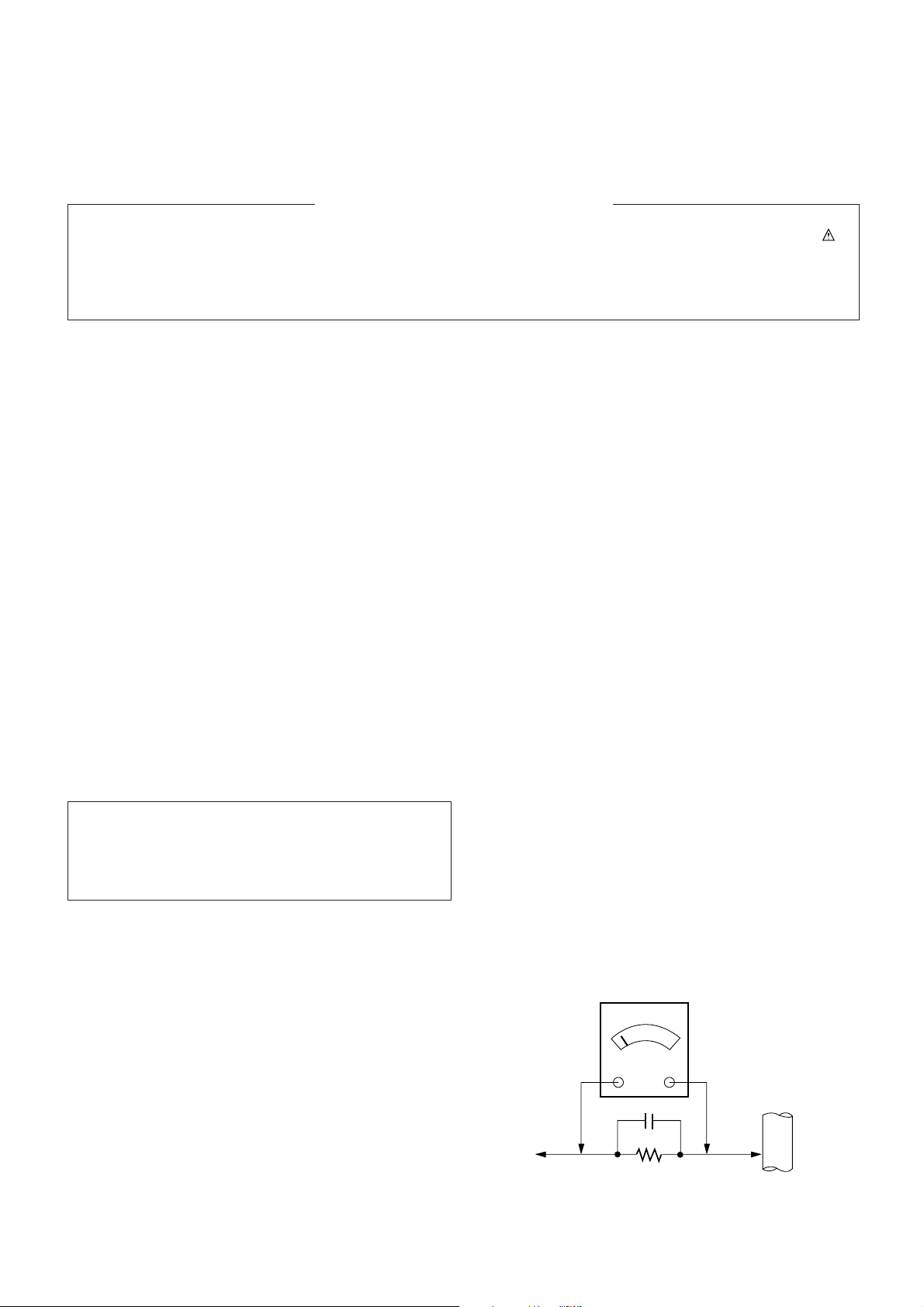
Leakage Current Hot Check (See below Figure)
Plug the AC cord directly into the AC outlet.
Do not use a line Isolation Transformer during this check.
Connect 1.5K/10watt resistor in parallel with a 0.15uF capacitor
between a known good earth ground (Water Pipe, Conduit, etc.)
and the exposed metallic parts.
Measure the AC voltage across the resistor using AC
voltmeter with 1000 ohms/volt or more sensitivity.
Reverse plug the AC cord into the AC outlet and repeat AC
voltage measurements for each exposed metallic part. Any
voltage measured must not exceed 0.75 volt RMS which is
corresponds to 0.5mA.
In case any measurement is out of the limits specified, there is
possibility of shock hazard and the set must be checked and
repaired before it is returned to the customer.
Leakage Current Hot Check circuit
The source of X-RAY RADIATION in this TV receiver is the
High Voltage Section and the Picture Tube.
For continued X-RAY RADIATION protection, the
replacement tube must be the same type tube as specified in
the Replacement Parts List.
1.5 Kohm/10W
To Instrument's
exposed
METALLIC PARTS
Good Earth Ground
such as WATER PIPE,
CONDUIT etc.
AC Volt-meter
IMPORTANT SAFETY NOTICE
0.15uF
Page 4

- 4 -
CAUTION: Before servicing receivers covered by this service
manual and its supplements and addenda, read and follow the
SAFETY PRECAUTIONS
on page 3 of this publication.
NOTE:
If unforeseen circumstances create conflict between the
following servicing precautions and any of the safety
precautions on page 3 of this publication, always follow the
safety precautions. Remember: Safety First.
General Servicing Precautions
1. Always unplug the receiver AC power cord from the AC
power source before;
a. Removing or reinstalling any component, circuit board
module or any other receiver assembly.
b. Disconnecting or reconnecting any receiver electrical plug
or other electrical connection.
c.
Connecting a test substitute in parallel with an electrolytic
capacitor in the receiver.
CAUTION: A wrong part substitution or incorrect
polarity installation of electrolytic capacitors may result
in an explosion hazard.
d. Discharging the picture tube anode.
2. Test high voltage only by measuring it with an appropriate
high voltage meter or other voltage measuring device (DVM,
FETVOM, etc) equipped with a suitable high voltage probe.
Do not test high voltage by "drawing an arc".
3. Discharge the picture tube anode only by (a) first connecting
one end of an insulated clip lead to the degaussing or kine
aquadag grounding system shield at the point where the
picture tube socket ground lead is connected, and then (b)
touch the other end of the insulated clip lead to the picture
tube anode button, using an insulating handle to avoid
personal contact with high voltage.
4. Do not spray chemicals on or near this receiver or any of its
assemblies.
5. Unless specified otherwise in this service manual, clean
electrical contacts only by applying the following mixture to
the contacts with a pipe cleaner, cotton-tipped stick or
comparable nonabrasive applicator; 10% (by volume)
Acetone and 90% (by volume) isopropyl alcohol (90%-99%
strength)
CAUTION: This is a flammable mixture.
Unless specified otherwise in this service manual, lubrication
of contacts in not required.
6. Do not defeat any plug/socket B+ voltage interlocks with
which receivers covered by this service manual might be
equipped.
7. Do not apply AC power to this instrument and/or any of its
electrical assemblies unless all solid-state device heat sinks
are correctly installed.
8. Always connect the test receiver ground lead to the
receiver chassis ground before connecting the test receiver
positive lead.
Always remove the test receiver ground lead last.
9.
Use with this receiver only the test fixtures specified in this
service manual.
CAUTION: Do not connect the test fixture ground strap to
any heatsink in this receiver.
Electrostatically Sensitive (ES) Devices
Some semiconductor (solid state) devices can be damaged
easily by static electricity. Such components commonly are
called
Electrostatically Sensitive (ES) Devices.
Examples of
typical ES devices are integrated circuits and some fieldeffect
transistors and semicounductor "chip" components. The
following techniques should be used to help reduce the
incidence of component damage caused by static by static
electricity.
1. Immediately before handling any semiconductor component
or semiconductor-equipped assembly, drain off any
electostatic charge on your body by touching a known earth
ground. Alternatively, obtain and wear a commercially
available discharging wrist strap device, which should be
removed to prevent potential shock reasons prior to
applying power to the unit under test.
2. After removing an electrical assembly equipped with ES
devices, place the assembly on a conductive surface such as
aluminum foil, to prevent electrostatic charge buildup or
exposure of the assembly.
3. Use only a grounded-tip soldering iron to solder or unsolder
ES devices.
4. Use only an anti-static type solder removal device. Some
solder removal devices not classified as "anti-static" can
generate electrical charges sufficent to demage ES devices.
5. Do not use freon-propelled chemicals. These can generate
electrical charges sufficient to damage ES devices.
6. Do not remove a repalcement ES device from its protective
package until immediately before you are ready to install it.
(Most replacement ES devices are packaged with leads
electrically shorted together by conductive foam, aluminum
foil or comparable conductive material).
7. Immediately before removing the protective material from
the ieads of a replacement ES device, touch the protective
material to the chassis or circuit assembly into which the
device will be installed.
CAUTION:Be sure no power is applied to the chassis or
circuit, and observe all other safety precautions.
8. Minimize bodily motions when handling unpackaged
replacement ES devices. (Otherwise harmless motion such
as the bruching together of your clothes fabric or the lifting
of your foot from a carpeted floor can generate static
electricity sufficient to damage an ES device.)
General Soldering Guidelines
1. Use a grounded-tip, low-wattage soldering iron and
appropriate tip size and shape that will maintan tip
temperature within the range or 500¡£F to 600¡£F.
2. Use an appropriate gauge of RMA resin-core solder
composed of 60 parts tin/40 parts lead.
3. Keep the soldering iron tip clean and well tinned.
4. Thorohly clean the surfaces to be soldered. Use a mall
wirebristle (0.5 inch, or 1.25cm) brush with a metal handle.
Do not use freon-propelled spray-on cleaners.
5. Use the following unsoldering technique
a. Allow the soldering iron tip to reach normal temperature.
(500¡£F to 600¡£F)
b. Heat the component lead until the solder melts.
c. Quickly draw the melted solder with an anti-static,
suction-type solder removal device or with solder braid.
CAUTION: Work quickly to avoid overheating the
circuiboard printed foil.
6. Use the following soldering technique.
a. Allow the soldering iron tip to reach a normal
temperature (500¡£F to 600¡£F)
b. First, hold the soldering iron tip and solder the strand
against the component lead until the solder melts.
SERVICING PRECAUTIONS
Page 5

- 5 -
c. Qulckly move the soldering iron tip to the junction of the
component lead and the printed circuit foil, and hold it
there only until the solder flows onto and around both the
component lead and the foil.
CAUTION: Work quickly to avoid overheating the circuit
board printed foil.
d. Closely inspect the solder area and remove any excess
or splashed solder with a small wire-bristle brush.
IC Remove/Replacement
Some chassis circuit boards have slotted holes (oblong) through
which the IC leads are inserted and then bent flat against the
circuit foil. When holes are the slotted type, the following
technique should be used to remove and replace the IC. When
working with boards using the familiar round hole, use the
standard technique as outlined in parapraphs 5 and 6 above.
Removal
1. Desolder and straighten each IC lead in one operation by
gently prying up on the lead with the soldering iron tip as the
solder melts.
2. Draw away the melted solder with an anti-static suctiontype solder removal device (or with solder braid) before
removing the IC.
Replacement
1. Carefully insert the replacement IC in the circuit boare.
2. Carefully bend each IC lead against the circuit foil pad and
solder it.
3. Clean the soldered areas with a small wire-bristle brush.
(It is not necessary to reapply acrylic coating to the areas).
"Small-Signal" Discrete Transistor
Removal/Replacement
1. Remove the defective transistor by clipping its leads as
close as possible to the component body.
2. Bend into a "U" shape the end of each of three leads
remaining on the circuit board.
3. Bend into a "U" shape the replacement transistor leads.
4. Connect the replacement transistor leads to the
corresponding leads extending from the circuit board and
crimp the "U" with long nose pliers to insure metal to metal
contact then solder each connection.
Power Output, Transistor Device
Removal/Replacement
1. Heat and remove all solder from around the transistor leads.
2. Remove the heatsink mounting screw (if so equipped).
3. Carefully remove the transistor from the heat sink of the
circuit board.
4. Insert new transistor in the circuit board.
5. Solder each transistor lead, and clip off excess lead.
6. Replace heatsink.
Diode Removal/Replacement
1. Remove defective diode by clipping its leads as close as
possible to diode body.
2. Bend the two remaining leads perpendicula y to the circuit
board.
3. Observing diode polarity, wrap each lead of the new diode
around the corresponding lead on the circuit board.
4. Securely crimp each connection and solder it.
5. Inspect (on the circuit board copper side) the solder joints of
the two "original" leads. If they are not shiny, reheat them
and if necessary, apply additional solder.
Fuse and Conventional Resistor
Removal/Replacement
1. Clip each fuse or resistor lead at top of the circuit board
hollow stake.
2. Securely crimp the leads of replacement component around
notch at stake top.
3. Solder the connections.
CAUTION: Maintain original spacing between the replaced
component and adjacent components and the circuit board
to prevent excessive component temperatures.
Circuit Board Foil Repair
Excessive heat applied to the copper foil of any printed circuit
board will weaken the adhesive that bonds the foil to the circuit
board causing the foil to separate from or "lift-off" the board.
The following guidelines and procedures should be followed
whenever this condition is encountered.
At IC Connections
To repair a defective copper pattern at IC connections use the
following procedure to install a jumper wire on the copper
pattern side of the circuit board. (Use this technique only on IC
connections).
1. Carefully remove the damaged copper pattern with a sharp
knife. (Remove only as much copper as absolutely
necessary).
2. carefully scratch away the solder resist and acrylic coating
(if used) from the end of the remaining copper pattern.
3. Bend a small "U" in one end of a small gauge jumper wire and
carefully crimp it around the IC pin. Solder the IC connection.
4. Route the jumper wire along the path of the out-away
copper pattern and let it overlap the previously scraped end
of the good copper pattern. Solder the overlapped area and
clip off any excess jumper wire.
At Other Connections
Use the following technique to repair the defective copper
pattern at connections other than IC Pins. This technique
involoves the installation of a jumper wire on the component
side of the circuit board.
1. Remove the defective copper pattern with a sharp knife.
Remove at least 1/4 inch of copper, to ensure that a
hazardous condition will not exist if the jumper wire opens.
2. Trace along the copper pattern from both sides of the
pattern break and locate the nearest component that is
directly connected to the affected copper pattern.
3. Connect insulated 20-gauge jumper wire from the lead of
the nearest component on one side of the pattern break to
the lead of the nearest component on the other side.
Carefully crimp and solder the connections.
CAUTION: Be sure the insulated jumper wire is dressed so
the it does not touch components or sharp edges.
Page 6
- 6 -
SPECIFICATIONS
NOTE : Specifications and others are subject to change without notice for improvement.
A Scope
This specification can be applied to all the Projection television related to MP-03AB Chassis.
A Test Conditin
Conduct the test as mentioned below.
1) Temperature : 25¡ 5
°C
2) Relative Humidity : 65¡ 10%
3) Power Voltage : Standard input voltage (230V~, 50Hz)
But Standard input voltage mark value is marked by model.
4) Use the parts only designated in B.O.M.,PARTS SPEC.,or drawings.
5) Follow each drawing or spec for spec and performance of parts,based upon P/N of RPL
6)
Warm up TV set for more than 60min before the
measurement.
A Test and Inspection Method
1) Performance : Follow the Standard of LG TV test
2) Extra requirement
Chassis
MP-03AB
RE-44NA14T/13RB
RE-40NZ60RB
RT-44NA13RB/23RB
RT-40NZ60RB/RP
RT-44NA43RB/RP
RL-44NA14T/13RB
RL-40NZ60RB
Europe (except Fance)
China, Asia, Afreca,
Middle East
France
LG
‘T’/ ‘RB’ : Teletext option
Model Name Market Place Brand Remark
Model
RE/RL-44NA14T
RE/RL-40NZ60RB
Market
EUROPE
Remark
SAFETY : CB
CE EMI : EN55013
EMS : EN55020
Appliance
OK
Page 7
- 7 -
A Test and Inspection Method
Item
Recieving System
Available Channel
Input Voltage
Market
Screen Size
Aspect Ratio
Tuning System
TUNER IF
Operating Environment
Storage Environment
No
1
2
3
4
5
6
7
8
9
10
Remark
AV can be input NTSC-M
S (RL model for Fance)
S (RT model w/o China)
S (RE,RL, China model)
S (With Teletext model)
S (W/O Teletext model)
Specification
PAL, SECAM-BG
PAL, SECAM-DK, PAL-I
PAL, SECAM-BG
SECAM-LL’
PAL, SECAM-BG,
PAL, SECAM-DK, PAL-I
NTSC-M
1) VHF : E2 ~ E12
2) UHF : E21 ~ E69
3) CATV : S1~S20
4) HYPER : S21~S41
LL’VHF : B,C,D
AC 110-240V~, 50/60Hz
AC 230V~, 50/60Hz
Europe except France
France
Asia, Africa, Middle East
44/49/54, 39/40/45/50/57 inch
4:3, 16:9
FVS 100 Program
FVS 200 Program
38.9MHz, 39MHz
1)Temperature : -5 ~ 40 °C
2) Humidity : 30 ~ 95 %
3) Temperature :-20 ~ 50 °C
4) Humidity : 30 ~ 95 %
RE
RL
RT
(S Mark : Option Item)
RE
RL
RT
Page 8

A Feature and Function
- 8 -
Item
Feature AV Input
AV Output
Component Input
S-Video Input
SCART
key Local Key
Remocon
Picture PSM
User Control
DRPC
VM
Convergence
Sound SSM
AVL
DBS
TV Speaker
Balance
Timer Clock
Off time
On time
Auto sleep
Special Language
Input
PIP Input
child lock
Etc. Convergence
Comb Filter
SVM
ARC
ACMS
Auto Off
Teletext
No
1
2
3
4
5
6
7
Remark
Side
S (Rear, RT model)
S (Rear, RT model)
Rear 480i/ 480P/ 576i
(1080i for CHINA)
side 1, Rear 1
S (Rear, RE,RL model)
Front
S INDEX (With Index)
Tint : NTSC system only
S
S 3*3 EDC
S Dolby virtual (Option)
S
S S-VIDEO4 (EU ONLY)
S S-VIDEO4 (EU ONLY)
S
S
S
S
Specification
1 V/L/R
2 V/L/R
1 V/L/R
2 COMPONENT1, L/R
COMPONENT2, L/R
2 Y/C
3 Full SCART (with RGB Input) : 1
Half SCART : 1 (AV In/Out)
Half SCART ; 1 (AV In, YC In)
POWER, MENU, VOL(
F,G), PR(D,E)
TV/AV, OK, MUTE (W/O Index)
NEC Code
Dynamic/ Standard/ Mild/ Game/ User
Contrast/ Brightness/ Colour/ Sharpness/ Tint
On/ Off
1/ 2/ 3/ 4
1[+] Point/ 9[+] Point
Auto Convergence (option)
Dolby Virtual/ Flat/ Music/ Movie/ Speech/ User
On/ Off
On/ Off
On/ Off
L 50 ~ 0 ~ R 50
-- : -- AM
-- : -- AM Off (On)
-- : -- AM Pr 1 VOL 30 Off(On)
On/ Off
Multi language
TV/ AV1/ AV2/ AV3/ AV4/ S-VIDEO4/
Component1/ Component2
TV/ AV1/ AV2/ AV3/ AV4/ S-VIDEO4
On/ Off
MANUAL ADJUST
Auto Adjust
Digital comb filter
O
4:3/ 16:9 (4:3 Model)
16:9/ 14:9/ ZOOM/ AUTO/ 4:3 (16:9 Model)
O
On/ Off
TOP/ FLOF/ LIST
Page 9
- 9 -
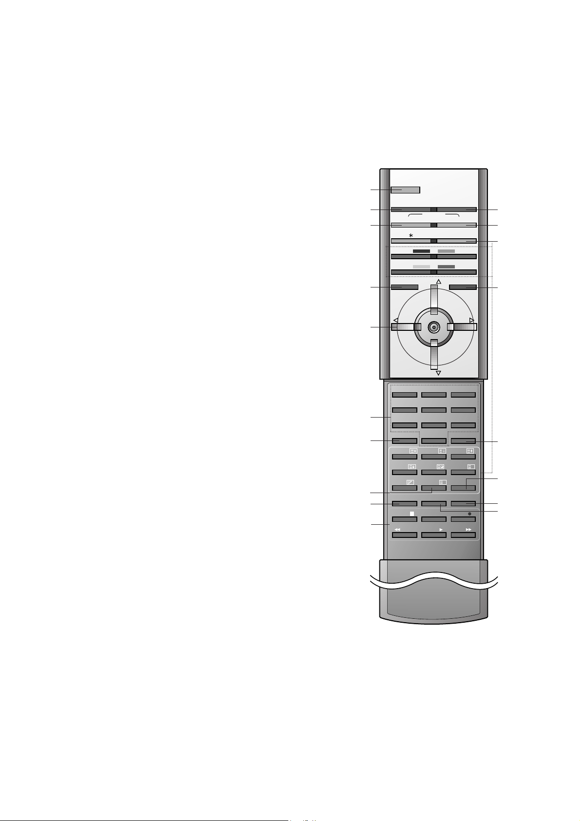
CONTROLS DESCRIPTION
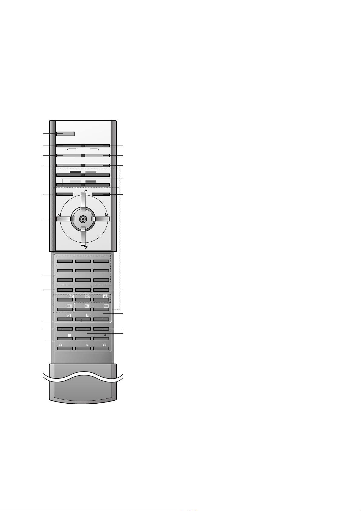
All the functions can be controlled with the remote control handset.
Some functions can also be adjusted with the buttons on the front
panel of the set.
Remote control handset
Before you use the remote control handset, please install the batteries. See the next page.
1. POWER
switches the set on from standby or off to standby.
2. TV/AV
selects TV or AV mode.
switches the set on from standby.
3. TURBO SOUND BUTTON
selects Turbo sound.
4. PIP BUTTONS (option)
PIP
switches the sub picture on or off.
PR +/-
selects a programme for the sub picture.
SWAP
alternates between main and sub picture.
INPUT
selects the input mode for the sub picture.
SIZE
adjusts the sub picture size.
STILL
freezes motion of the sub picture.
POSITION
relocates the sub picture in clockwise direction.
SCAN
switches on or off the programme scan mode 12 sub pictures.
5. MENU
selects a menu.
6.
D / E
(Programme Up/Down)
selects a programme or a menu item.
switches the set on from standby.
F / G
(Volume Up/Down)
adjusts the volume.
adjusts menu settings.
OK
accepts your selection or displays the current mode.
7. NUMBER BUTTONS
switches the set on from standby or directly select a number.
8. PSM (Picture Status Memory)
recalls your preferred picture setting.
9. SLEEP
sets the sleep timer.
10. I/II
selects the language during dual language broadcast.
selects the sound output (option).
11. VCR BUTTONS
control a LG video cassette recorder.
123
456
7
PSM SSM
8
0
POSITION
STILL
SCAN
MIX
REVEAL
?
M
TIME
SIZE
LIST
SLEEP
I/II ARC
Q.VIEW
STOP REC
P/STILL
REW FF
PLAY
9
POWER
TV/AV MULTIMEDIA
SOUND PICTURE
TURBO
PIP TEXT
PR
- PR +
INPUTSWAP
MENU PR
VOL
OK
VOL
PR
MUTE
1
12
13
14
16
17
18
19
20
15
2
3
4
5
6
7
8
10
9
11
(With TELETEXT/PIP)
Page 10
- 10 -
12. MULTIMEDIA
selects Component 1 or Component 2 modes.
switches the set on from standby.
13. TURBO PICTURE BUTTON
selects Turbo picture.
14. TELETEXT BUTTONS (option)
These buttons are used for teletext.
For further details, see the ‘Teletext’ section.
15. SWAP
returns to the previously viewed programme.
selects a favourite programme.
16. MUTE
switches the sound on or off.
17. SSM (Sound Status Memory)
recalls your preferred sound setting.
18. LIST
displays the programme table.
19.
ARC (Aspect Ratio Control)
select your desired picture format.
20. Q.VIEW
returns to the previously viewed programme.
selects a favourite programme.
*
: No function
COLOURED BUTTONS : These buttons are used for teletext (only
TELETEXT models) or programme edit.
Note : In teletext mode, the PR +/-, SWAP and INPUT buttons are
used for teletext function.
1 2 3
4 5 6
7
PSM SSM
8
0
UPDATE
HOLD
INDEX
MIX
REVEAL
?
M
TIME
SIZE
LIST
SLEEP
I/II ARC
Q.VIEW
STOP REC
P/STILL
REW FF
PLAY
9
POWER
TV/AV MULTIMEDIA
SOUND PICTURE
TURBO
TEXT
MENU PR
VOL
OK
VOL
PR
MUTE
1
12
13
14
16
17
18
19
20
2
3
5
6
7
8
10
11
(With TELETEXT/Without PIP)
9
Page 11
- 11 -
S-VIDEO VIDEO
L/MONO RAUDIO
AV3
11
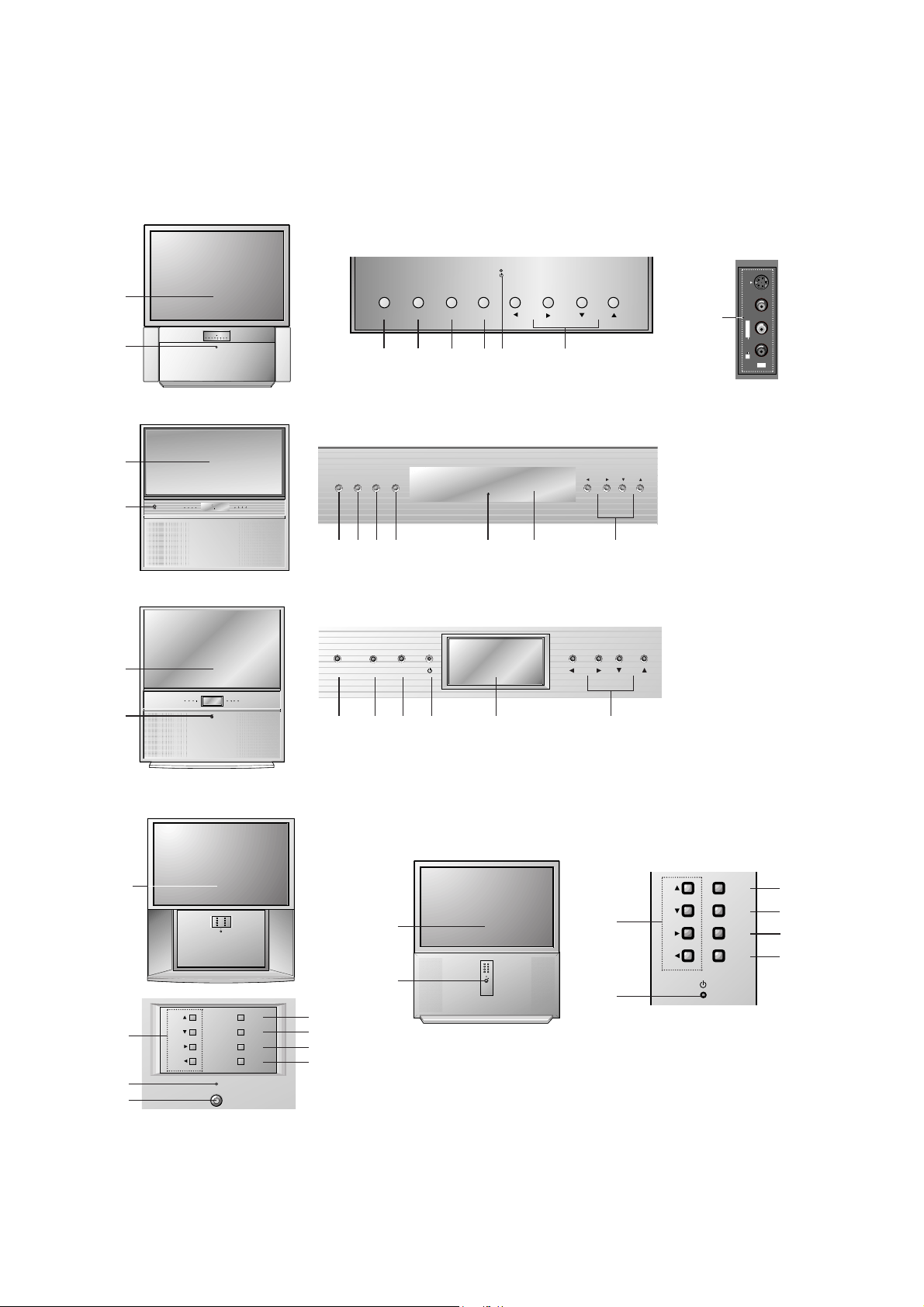
Front panel
ON/OFF
PR
MENU MUTE
TV/AV
VOL
OK
PR
MENU MUTE
TV/AV
VOL
OK
8
1
•
RE/RL-44/49/54NA13/14 series
7
6
5
4
23
•
RE/RL-44/54NA23/24 series
TV/AV OK INDEX VOL PRMENU
8
1
•
RE/RL-39NZ43 series
TV/AV OK INDEX
VOL PR
MENU
7 6 5 9 3 10 2
TV/AV
MENU
OK
VOL
PR
TV/AV MENU
VOL PR
OK
8
716 5 3 10 2
•
RE/RL-44/49/54NZ23 series
ON/OFF
PR
PR
VOL
VOL
MUTE
MENU
OK
TV/AV
2
4
6
5
7
ON/OFF
PR
PR
VOL
VOL
MUTE
MENU
OK
TV/AV
8
1
3
•
RE/RL-44/54NA43/44 series
PR
PR
VOL
VOL
POWER
MUTE
MENU
OK
TV/AV
8
1
PR
PR
VOL
VOL
MUTE
MENU
OK
TV/AV
2
3
4
6
5
7
(Side panel)
Page 12
- 12 -
1. MAIN POWER (ON/OFF)
switches the set on or off.
2.
FF / GG
(Volume Up/Down)
adjusts the volume.
adjusts menu settings.
DD / EE
(Programme Up/Down)
selects a programme or a menu item.
switches the set on from standby.
3. POWER/STANDBY INDICATOR
illuminates brightly when the set is in standby
mode.
dims when the set is switched on.
4. MUTE (option)
switches the sound on or off.
5. OK
accepts your selection or displays the current
mode.
6. MENU
selects a menu.
7. TV/AV
selects TV or AV mode.
switches the set on from standby.
8. REMOTE CONTROL SENSOR
9. INDEX (option)
switches LED DISPLAY on or off.
10. LED (Light Emitting Diode) DISPLAY
(option)
illuminates brightly when the set is switched
on.
Option : Only RE/RL-39NZ43 series,
: PAL/SECAM indicator
: NTSC indicator
: STEREO indicator
: SLEEP Timer indicator
: CHILD LOCK indicator
11. AUDIO/VIDEO IN SOCKETS (AV3)
Connect the audio/video out sockets of external equipment to these sockets.
S-VIDEO/AUDIO IN SOCKETS (S-AV)
Connect the video out socket of an S-VIDEO
VCR to the S-VIDEO socket.
Connect the audio out sockets of the SVIDEO VCR to the audio sockets as in AV3.
*
CASTERS (on the bottom)
turn and move the set easily.
Front panel
S-VIDEO VIDEO
L/MONO AUDIO
AV3
R
(Side panel)
11
PR
MENU
MUTE
TV/AV
VOL
OK
8
1
•
RE/RL-39/45/56NZ60 series
PR
MENU MUTE
TV/AV
VOL
OK
7 6 5 4 3 2
STEREO
SLEEP
LOCK
Page 13
- 13 -
These instructions are applied to only MP-03AB chassis.
Notes
1.Because this is not a hot chassis, it is not necessary to use an
isolation transformer.
However, the use of isolation transformer will help protect
test instrument.
2.Adjustment must be done in the correct order.
3.The receiver must be operated for about 60 minutes proir to
the adjustment.
Pre-heatrun must be operated receiving moving pictures or
100% white pattern.
[ Never operate the SET over 10 minutes with still picture
because a fluorescent material may get damage.
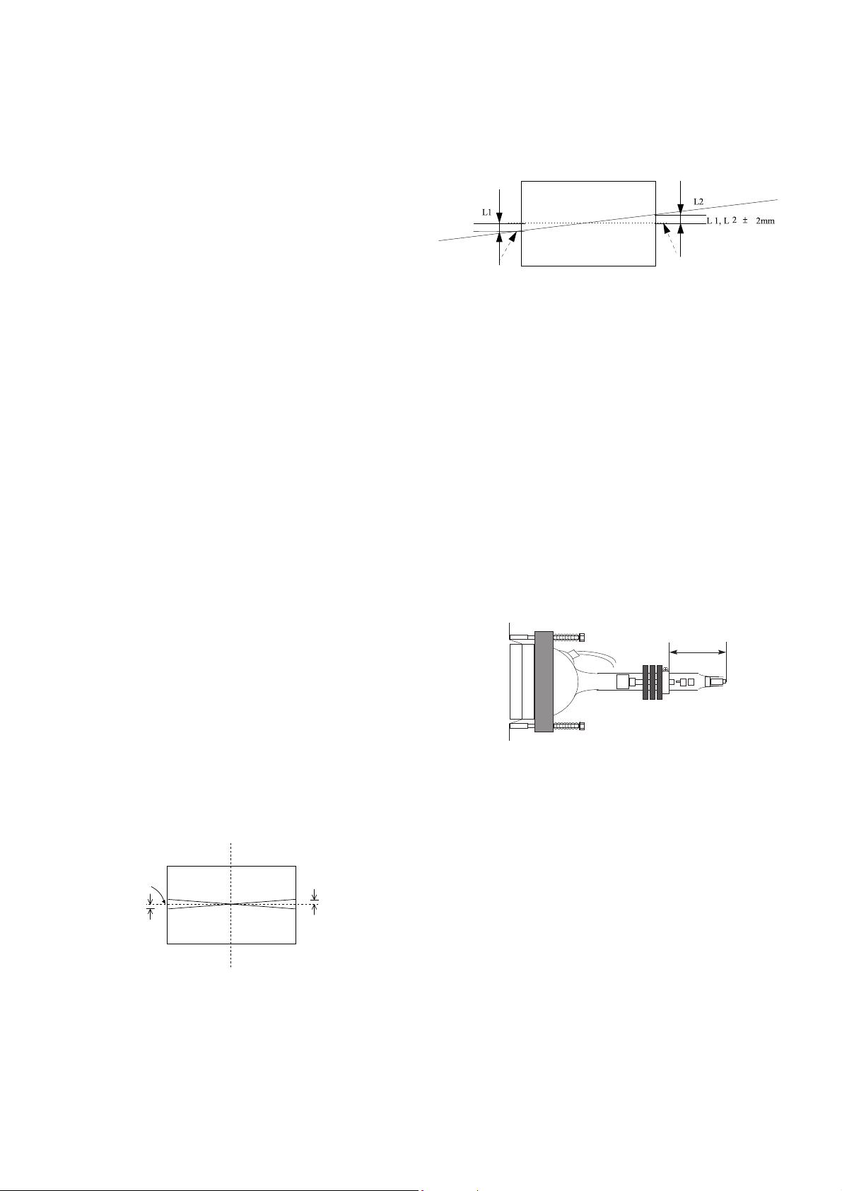
O Raster Slope/Focus 1th Adjustment
1. Preliminary steps
1) Apply power to the unit and switch the unit ON.
2) Receive the EU 05 CH signal.
3) Select INSTART key on the Remote Control and then select
“0 RASTER ADJ” move the cursor or by pressing the key
No. 0.
4) Adjust Lens Focus/Electric focus temporarily.
[ When select “0 RASTER ADJ” mode after entering adjustment
mode with INSTART key, the convergence reset and then
preparation for adjustment complete.
[ The convergence reset is possible even from convergence
adjustment mode.
1) Enter into convergence adjustment mode: Select INSTART
key on the Remote Control and then select “3
CONVERGENCE” move the cursor or using the key No..
2) Convergence reset: After press the key No. 5, press the
ENTER key.
3) Adjustment mode release: Press the INSTART key
2. Adjustment
1) Display only the Green raster using lens covers to block Red
and Blue.
2) Rotate the Green DY and tilt the screen like the figure below.
3) Make 2color raster with Red or Blue and Green.
4) Coincide the slope of red and blue raster to that of green.
Note) 1. When adjusting raster slope, loosen the DY and fasten
itafter adjusting.
2. Never rotate and adjust the fixed DY without loosing it.
O Beam Alignment Adjustment
1. Test Equipment
Video Test Generator(801GF) or Signal Generator can produce
NTSC DOT pattern(408NPS or 5518/5418 equipment)
2. Preparation
1) Heat run over 60 minutes.
2) Pre-adjust Raster slope,Raster position & Lens focus &
centering Magnet.
3) Check if the Magnet is located 45mm from the end of CRT.
4) In case of using 801GF : Receive #13 DOT Pattern of VGA
mode(Format #5) through PC input terminal.
In case of using NTSC generator : Receive Dot signal
through the external input terminal.
3. 2-Pole Magnet Adjustment
1) Make Green raster using lens cover.
2) Check the center position of DOT pattern on the center of the
screen after turning Green focus volume left.
3) Turning green focus volume right and adjust 2-Pole magnet
so the position to coincide that of item ”(2)”.
4) Adjust not to shift the screen by turning green focus volume
clockwise and counter clockwise.
5) If the screen shifts, readjust (2)~(4).
6) Do the same method in Red and Blue.
4. Beam Shape (4 & 6-Pole Magnet) Adjustment
1) Do after 2-Pole magnet adjustment.
2) Make Green raster using lens cover and turn the focus
volume right.
3) Make the dot in the center a perfect circle using 4 & 6-Pole
magnet.
4) Do the same method in Red & Blue.
5) Fasten the Magnet after adjustment.
6) Adjust focus accurately.
ADJUSTMENT INSTRUCTIONS
L
L
Mechanical
center
L ¡´!2mm
Red/Blue Light
Green Light
45mm
Page 14

O Centering Magnet Adjustment
1. Preliminary steps
1) Receive the EU 05 CH signal.(PR.1 : PAL B/G 175.25MHZ)
2)
Press the keys of Remote Controller for adjustment to reset the
convergence.
a.Adjustment mode:Press the IN-START key.
b.Data reset : Press 0 KEY.
c.Adjustment mode cancellation : Press the
ENTER
key.
2. Adjustment
1) Operate adjustment about Red,Green,Blue centering
magnet.
2) SGS-THOMSON Convergence assy
Adjust until the center of blue signal is shifted up to 40mm
left from that of green signal and center of red signal is
shifted up to 40mm right from that of green signal with
turning the centering magnet.
3) After adjustment, re-adjust convergence data and exit the
adjusting mode.
a.Adjustment mode:Press the IN_START key.
b.Data reset : Press 0 KEY.
c.Adjustment mode cancellation : Press the Enter key.
O High Voltage Regulation Adjustment
1. Test Equipment
Digital Multi-Meter(DMM)
2. Preparation for Adjustment.
Select picture mode to ‘DYNAMIC’ in no signal input.
3. Adjustment
1) Press the IN_START key and then press ‘1’ key.(HV ADS)
2) Connect “+” terminal(Red) of DMM to the P415 of the
Deflection PCB, [+] and the “-”terminal(Black) to the P416,[-].
3) Adjust VR401 so that the voltage of multimeter to be below
voltage.
Voltage : 21.7 ! 0.1V.
4) Exit the adjustment mode by pressing the enter key
O CUT-OFF Voltage Adjustment
1. Preliminary steps
(1) Select INSTART key on the Remote Control and then select
“2 SCREEN ADJ” move the cursor or using the key No..
(2) Adjustment must be operated in a dark room (simple dark
room)
2. Adjustment
1) Test Equipment: Oscilloscope, 100:1 Probe
2) Connect oscilloscope to cathode of R, G, B(R926R/B/G:
SCREEN ADJ on the PCB) and GND.
3) Turning Screen Volume (R/G/B) in Focus Pack and adjust
R/G/B is 165V!0.5V.
4) After adjustment complete, exit the RASTER adjustment
mode using ENTER key and exit the SVC adjustment mode
using INSTART key.
O Deflection Adjustment
1. Preliminary steps
1) NTSC mode should be adjusted after adjusting PAL mode.
2) PAL adjustment should be done in the EU CH05,and NTSC
adjustment should be done in the CH13 or Multi 48CH.
Note, RE/RL Model(without NTSC-M system) receive CH13
in the V-3 input.
3) Press the button of Remote Controller for adjustment to reset
the convergence
Adjustment Mode : Press the IN_START key
Data reset : Press the 0 key.
Saving and returning Adjustment mode : Press the ENTER
Key
Note. Refer adjustment items to Appendix1.
2. PAL Mode Deflection adjustment
Do not adjust H-POS,V-POS, V-LIN, S-COR, A-BOW, A-ANG,
UCPIN, LCPIN, V-ASP,V-SCR in PAL mode.
Select the below each mode using CH
D, E and adjust using
VOL
F, G on the remote controller.
At SVC mode, press the ‘0’ key get into the deflection
adjustment mode.
1) H-POS (Horizontal Position Adjustment)
Adjust so that the horizontal center line of screen is in accord
with the geometric horizontal center ine of screen JIG.
2) V-POS (Vertical Position Adjustment)
Adjust so that the vertical center line of picture is in accord
with the vertical center line of the screen.
3) HSIZE (Horizontal SIZE Adjustment)
Adjust so that the outermost left and right vertical line of the
screen is accord with the last point of the frame
4) VSIZE (Vertical SIZE Adjustment)
Adjust until Sixth vertical center line from upper and lower
center of the picture is accord with the last point of the frame.
5) U-VL (Upper Vertical Linearity Adjustment)
Adjust
the vertical interval of screen upper.
6) L-VL (Lower Vertical Linearity Adjustment)
Adjust
the vertical interval of screen lower.
- 14 -
0V
165V±0.5V
2 Pole Magnet
4 Pole Magnet
6 Pole Magnet
Page 15
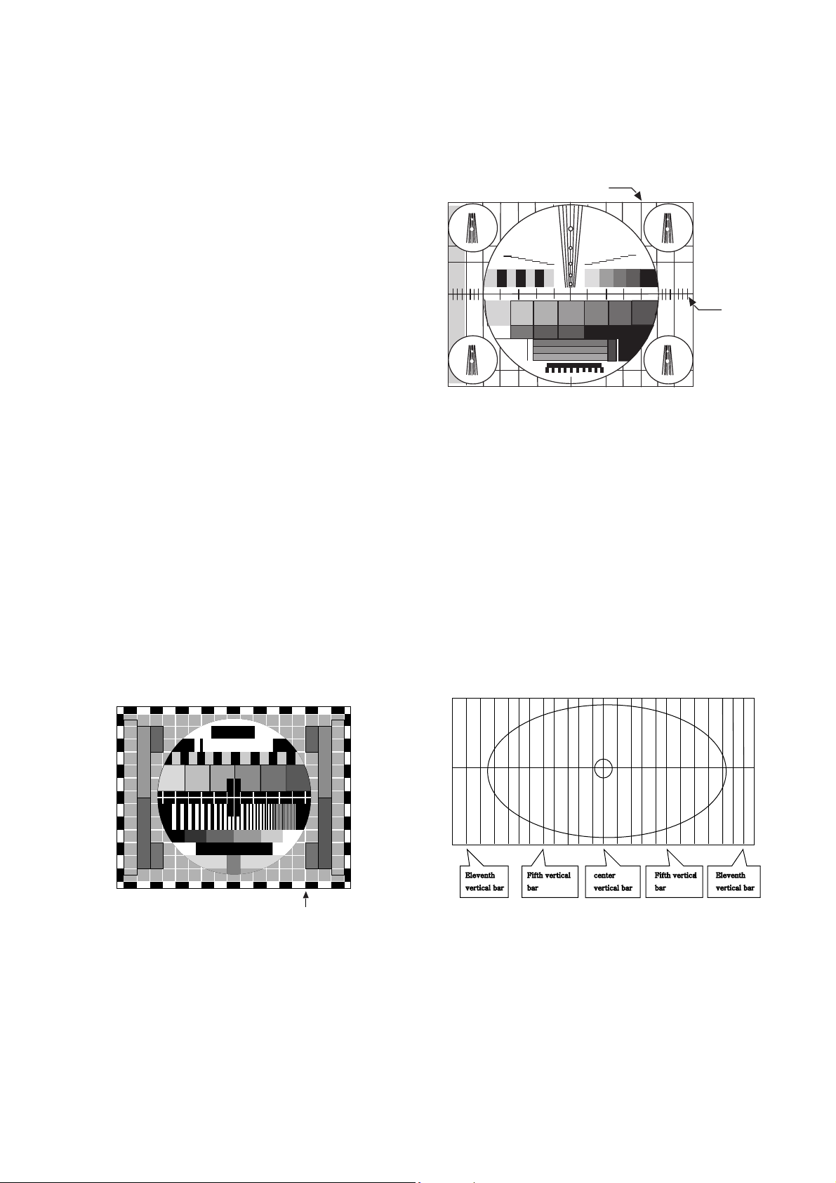
7) PIN-P (Horizontal Trapezoid Distortion Compensation
Adjustment)
Adjust to ake the length of top horizontal line same with it of the
bottom horizontal line.
8) PIN-A (Horizontal PIN Distortion Compention Amount
Adjustment)
Adjust the horizontal width of picture upper and lower is to be
same.
9) V-LIN (Vertical Linearity Adjustment)
Adjust vertical size of the picture to be same with upper and
lower.
10) S-COR (Vertical S Correction)
Adjust so that all distance between each horizontal lines are to
be the same.
11) A-BOW (AFC BOW)
Adjust so that the vertical line at every 4 corners of the screen
look like parallel with the vertical center lines of picture.
12) A-ANG (AFC Angle)
Adjust so that all vertical slope of the picture are vertical.
13) UCPIN (Upper Corner Pincushion)
The pin cushion adjustment of upper part
14) LCPIN (Lower Corner Pincushion)
The pin cushion adjustment of lower part
15) V-ASP(Vertical Aspect Ratio)
Adjust the vertical aspect ratio.
16) V-SCR (Vertical Scroll)
Adjust the vertical aspect position.
Store the adjusted data in EEPROM by pressing the ENTER key
before exiteng adjustment mode.
Exit the adjustment mode by pressing the ENTER key.
3. NTSC Mode Deflection Adjustment
Do not adjust V-LIN, S-COR, A-BOW, A-ANG, UCPIN, LCPIN,
V-ASP, V-SCR in NTSC mode.
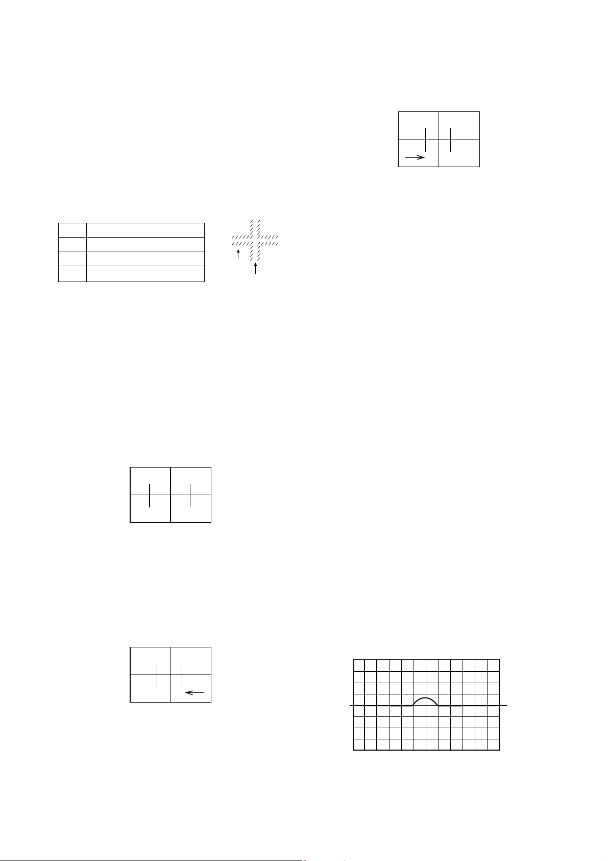
1) Adjust vertical size (V-SIZE Adjustment) until fifth vertical bar
from upper and lower center screen is accord with the edge
of the frame.
2) Adjust horizontal size (H-SIZE Adjustment) until third bar to
indicate horizontal size of circle is accord with the edge of
the frame.
3) Do other adjustments the same as in PAL mode.
4. 1080i Mode deflection Adjustment (option)
(1) Test Equipment
SETTOP BOX with 1080i output or MSPG-925LTH
(Programmael VIDEO Singnal Generator).
(2) Preliminary steps
1) After adjust 1080i with output of the SETTOP BOX,
connects to AV-3 (Side-AV) the Y signal only which is
output from SETTOP BOX with the VIDEO input terminal.
2) Select INSTART key on the Remote Control and then
select “5 1080I-ADJ” move the cursor or using the key
No.5.
3) Adjust vertical size (V-SIZE Adjustment) until fifth vertical
bar from upper and lower center screen is accord with the
edge of the frame.
4) Adjust horizontal size (H-SIZE Adjustment) until twelfth
vertical bar is accord with the edge of th frame.
5) Do other adjstments the same as in PAL mode
O
Lens Focus & Electronic Focus Adjustment
1. Preliminary steps
1) Electronic focus,Raster slope & Raster position must be preadjusted.
2) Heat-run over 60 minutes.
- 15 -
Third bar
Fifth vertical BAR
Sixth Vertical Line
<Fig. 3>
Page 16
3) Receive Crosshatch pattern.
(PAL:EU07(PR 8) or NTSC:09CH(PR 13))
* Note: Loosen the butterfly nut in the lens tub slightly,being
careful that it is mot loosened to the point that the lens can
move out of focus.
4) Adjustment must be done in a dark room(simple dark room)
Be careful not to touch the lens during adjustment.
5) Make any one color raster using lens covers.
6) Rotating lens right from the front side chromatic haze occurs
beside Cross-hatch line changes as follows;
2. G-lens Adjustment
1) Rotate the lens until the chromatic haze changes from blue to
red.
2)
Viewing the all screen, in no case of the chromatic aberration
appeared slimly within 3.5 cross-Hatch of the picture center. At
this time, in case that the red chromatic aberrations bright line
isn't equal, adjust Green lens so that the red chromatic
aberration is appeared more than previous time.
3) Switching the signal to 13CH and operate adjustment
minutely.
4) Adjust Green focus control volume of focus pack so that the
external big circle's part appeared clearly.
5) Adjust accurately by repeat the upper control.
6) Especially, noting to the Green light because it influenced on
picture’s function.
3. R-lens adjustment
1) Rotate the RED lens until the chromatic haze changes from
orange to scarlet.
2) Adjust to appear Red chromatic aberration in right 3.5 crosshatch section at center screen.Adjust the chromatic
aberration so that it located center correctly.
3) Switching the signal to 13CH and adjust it as same method of
Green lens.
4) Adjust as same method of Green lens with Red focus control
volume of focus pack.
4. B- lens adjustment
1) Rotate the lens until the chromatic aberration of 3.5 CrossHatch left from center point changes from Violet to Green.
Adjust the chromatic aberration to be center point between
violet and green.
2) Adjust as same as method of Green lens with Red focus
control volume of focus pack.
5. Focus checking
After adjustment Red,Green & Blue lens, remove lens cover
and receive Cross-Hatch pattern and check the overall focus. If
needed,repeat above.
O Convergence Adjustment
1. Preliminary steps
This adjustment should be performed after warming up 60
minutes.
1) Adjust after Horizontal/Vertical Raster position,Beam
alignment magnet, and focus adjustments have been
completed.
2) Do it always with crosshatch pattern.
3) Adjust for both PAL and NTSC system.
4) Use the JIG screen with the cross hatch pattern for
Adjustment.
2. Convergence Key
1) Convergence Mode : IN_START, ‘3’
2) Cursor shift :
F , G , D ,E
3) Cursor Movement/Adjustment Selection : ENTER
4) Cursor Color Selection : TV/AV
5) Adjustment mode out : IN_START
*Note: When cursor flashes,set is in adjustment mode When
R,G or B selected color flashes,the set is in cursor movement
mode.
O PAL Mode Adjustment
1. Preliminary steps
1) Receive the EU 05CH signal.
2) Press the buttons IN_START, ‘3’ of Remote Controller for
adjustment to get into the convergence adjustment mode.
2. Horizontal/Vertical phase adjustment
1) Press the buttons 9 & 5 to get into the phase adjustment
mode.
2) Horizontal Phase Adjustment.
Move the convex part to the quarter of vertical center by
pressing the Volume F,G key.
3) Press the ENTER Key to escape from the adjustment.
- 16 -
Lens
Red
Green
Blue
Change of chromatic aberration
Orange ¤AScarlet
Blue ¤ARed
Purple ¤AGreen
CHROMATIC
ABERRATION
CROSS HATCH
SIGNAL
Page 17
3. Pattern position adjustment
1) Change into pattern shift mode.
(Press numeric buttons “9” & “4”)
2) Make sure to overlap pattern and image.
(Use MUTE button)
3) Accord the center of image and pattern.
(Use
F , G , D ,E buttons)
4) Quit pattern shift mode. (Press “OK” button)
5) Save adjusted phase/pattern position adjustment
mode.(Press “9”, “2” & “OK” buttons)
4. Auto convergence (option)
*
Convergence is based on the auto adjustment using PC and
Camera while applying the THOMSON convergence Assy and if
need,adjust manually like below method.
5. Green convergence adjustment
1)
Show the OSD on screen by pressing 2 button,then change the
OSD to green(G) adjustment mode with pressing TV/AV button.
2) Close the cover of red PRT and blue PRT so that green
display on screen only.
3) Adjust to coincide green pattern with screen JIG pattern.
(Use
F , G , D ,E buttons)
At this time move cursor from center to around and adjust
convergence.
6. Red convergence adjustment
1)
Show the OSD on screen by pressing 2 button,then change the
OSD to red(R) adjustment mode with pressing TV/AV button.
2) If the need arises,close the cover of the blue lens.
3) Coincide the red screen with the green screen in same way
with that of green convergence adjustment.
7. Blue convergence adjustment
1)
Show the OSD on screen by pressing 2 button,then change the
OSD to blue(B) adjustment mode with pressing TV/AV button.
2) Coincide the blue screen with the green screen in same way
with that of red convergence adjustment.
8. Saving adjusted data
1) To save the data after adjustment,Press “9”, “1” & “OK”
button.
2) Quit convergence adjustment mode. (“IN_START” button)
9. NTSC mode adjustment
1) Receive the 13CH or Multi 48 CH signal.
2) Adjust as same method of PAL mode.
10. Auto-Convergence measuring or Measuring
back up data (option)
1) Operate the auto-convergence measuring or the measuring
back up data separately in PAL,NTSC mode.
2) Operate in the condition of ‘Zero magnetometer ‘ in room
after correcting convergence manually.
3) How to measuring
Press the ‘IN_START -> 3 ->MENU->3’ key to operate Auto
convergence measuring or the measuring back up data.
O White Balance Adjustment
1. Test Equipment
Brightness meter(CA110)
2. Adjustment
1) This adjustment must be operated in a dark room or
equivalent.
2) Adjust after Cut-Off and Focus adjustment.
3) The brightness meter must be located in 20¡ 5cm distance
from the center of the screen.
4) Receive WINDOW signal.
* High Light : RE/RL : 250!10
cd/m^2 (16:9)
RT : 160!10
cd/m^2 (16:9)
RE/RL : 190! 10
cd/m^2 (4:3)
RT : 160!10
cd/m^2 (4:3)
* Low Light : 10!3
cd/m^2
5) Set BRIGHT to H/Light adjustment mode in 4) and enter SVC
mode by pressing the “IN_START & 4” button. Adjust RG (R
Gain) and BG (B Gain) until color coordinate becomes
RE/RL - X=0.283 and Y=0.292, RT - X=0.269 and Y=0.274
(Deviation : !0.03).
6) Set BRIGHT to L/Light adjustment mode and adjust CR (R
Cut Off) and CB (B Cut Off) until color coordinate becomes
RE/RL - X=0.280 and Y=0.260, RT - X=0.269 and Y=0.274
(Deviation : !0.03).
7) Repeat adjusting until the color coordinate of H/Light and
L/Light is satisfied.
8) Save the data after adjustment. (Press “ENTER” button)
9) Exit adjustment mode. (“ INSTART ” button)
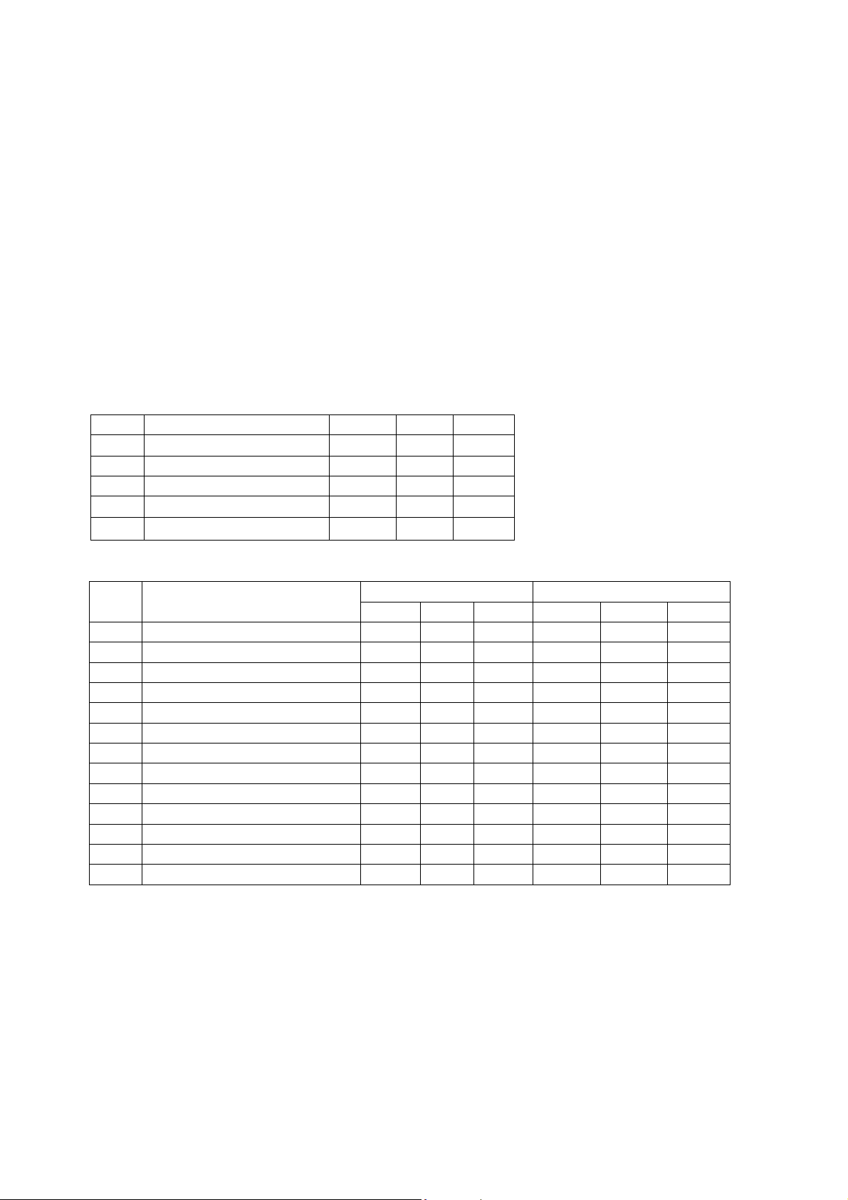
O Sub-Bright Adjustment
1) Tune the TV set to receive a EU 05 CH.
2) Enter WB mode by pressing the IN_START & ‘4’ button.
Adjust S-BRI data until 100% and 80% GRAY PATTERN is
classified.
(Use
F , G , D ,E, ENTER buttons)
O Auto-Convergence Check (option)
1) Check the Auto-Convergence in PAL/NTSC/1080i(option)
mode separating.
2) Press the IN_START key on R/C for adjustment and press
the CAPTION key to check whether Auto-Convergence
works normally in each mode.
3) If not,check the Convergence condition or Measuring
condition and SENSOR condition.
4)The shipment must be done after restoring the final auto
convergence data value.
* Restore a Convergence data
IN_START -> ‘3’
-> TEXT
- 17 -
Fifth Vertical Line
100% and 80% GRAY PATTERN
Page 18
- 18 -
O Check the Option Adjustment
1) Check the OPTION1~5 data of attach 6 is well recorded.
2) The option value of each suffix is started on JOB EXP of 3141VMN chassis Assy.
O Convergence Adjustment Mode
- INSTART -> 3
-> MENU
* This Mode is for engineering. So,don’t change before permission from Design Department.
0.AC POSITION READ : Distance data(After auto convergence measuring)
1.Save to 50Hz/60Hz : Save (convergence adjustment data)
It’s same 9,1,Enter.
2.Save Control data : Save (A phase adjustment data)
It’s same 9,2,OK.
3.AC Position Meas/ Meas backup data. : Execute( auto convergence measuring)
4.Pattern : Adjust location of convergence pattern.
It’s same 9,4,Enter.
5.Phase : Adjust a phase of convergence pattern.
It’s same 9,5,Enter.
6.GRID Border
7.ADJUST: Set the Dynamic focus data&auto-convergence data
HGD
HRD
VGD
BPH
BPV
29
42
44
22
35
27
55
23
20
18
Horizontal Grid Distance
Horizontal Retrace Distance
Vertical Grid Adjustment
Border Position Horizontal
Border Position Vertical
Item Description (PAL) (1080i)
27
55
38
18
26
(NTSC)
24
19
30
6
31
31
110
60
3
3
MICOM
NO
NO
29
23
31
9
31
31
110
60
3
3
MICOM
NO
NO
29
23
31
9
31
31
110
60
3
3
MICOM
NO
NO
30
27
32
13
31
31
110
60
3
3
MICOM
NO
NO
28
26
31
54
31
31
110
60
3
3
MICOM
NO
NO
30
27
32
0
31
31
110
60
3
3
MICOM
NO
NO
Item
Description
Focus parabola top value
Focus parabola middle value
Focus parabola bottom value
Focus parabola position
Start of the retrace value
Focus value during frame retrace
Force the video pattern fast blanking
Auto convergence offset
Pattern Bright Horizontal
Pattern Bright Vertical
EEPROM/MICOM selection
Initialization of AC Pattern data
Initialization of ADJ. Focus data
4:3 TV (WIDE = 0 )
PALNTSC 1080i NTSC PAL 1080i
16:9 TV (WIDE =1)
FV1
FV2
FV3
VFP
FSB
FVR
STA
ACO
PBH
PBV
OPT
ACINIT
ADJINIT
Page 19
8.OSD POSITION
9.AC PATTERN ADJ :Assign location for pattern start
O SVC Adjustment mode & Initial data
1. White Blalane adjustment data (IC:CXA2100)
2. Sound adjustment data (IC:MSP3411G)
- 19 -
8,17
10,15
11,14
11,16
13,17
13,17
9,5
10,7
10,9
17,16
17,15
18,17
14,17
14,17
15,16
18,9
18,8
19,6
H,V
H,V
4,7
3,7
3,6
6,18
5,20
4,18
H,V
10,33
12,31
13,28
14,27
15,29
15,30
12,5
13,6
13,10
14,30
14,32
15,33
11,31
11,29
12,29
15,11
15,9
16,10
H,V
H,V
5,17
3,15
3,15
6,28
5,28
4,28
H,V
<PAL mode> <NTSC mode>
• MDB(MICRONAS DYNAMIC BASS)
14
53
12
66
66
2D
19
09
OB
FC
FM
NP
SP
S1 VOL
S2 VOL
MDB-STR
MDB-HMC
MDB-HP
MDB-LP
MDB-LIM
Menu Description
FM Prescaler
NICAM Prescaler
SCART Prescaler
SCART 1 Volume
SCART 2 Volume
MDB Effect Bass Strength
MDB Harmonic Content
MDB High Pass
MDB Low Pass
MDB Amplitude Limit
Range Default
14
27
29
0D
1F
09
20
75
09
1F
2D
14
1F
13
20
75
RD
GD
BD
RC
GC
BC
S-BRI
DVCO
Menu
Description
Red Drive
Green Drive
Blue Drive
Red Cut-off
Green Cut-off
Blue Cut-off
Sub BRIGHT
Digital VCO
Range
Default
RE/RL RT
Page 20

- 20 -
03
00
00
00
03
01
02
03
02
00
01
02
03
02
0A
05
0B
07
1f
1f
07
00
00
00
02
02
03
00
00
D-COL
EXTSW
SHPFO
BLKBT
PREOV
CTILE
LTILE
PLMTL
ABLMO
CTI-M
LTI-M
GAMMA
DPIC
DC-TR
S-CON
LRGB2
P-ABL
ABLTH
CB-OF
CR-OF
Y-OFF
AGN-W
AGN-B
SYSTM
VM-DL
VM-FO
VM-LE
FLCOL
FL-SW
Menu Description
Dynamic color mode setting
Selects the Y/Cb/Cr input or EY/ECb/Ecr
Sharpness f0 setting
RGB output bottom limiter level control (for blanking/signal)
Pre-shoot/over-shoot ratio setting
CTI level setting
LTI level setting
RGB output amplitude level setiing
ABL mode setting
CTI mode setting
LTI mode setting
RGB output GAMMA correction amount control
Dynamic picture(black expansion) control
Y system DC transmission ratio setting
Sub Contrast control
Picture level control for LRGB2
RGB output level detection DC setting for PEAK ABL
Threshold voltage adjustment for ABL_IN input
DC_OFFSET canceling for Cb signal
DC_OFFSET canceling for Cr signal
DC_OFFSET canceling for Y signal
White(80IRE) output aging mode ON/OFF switch
All blank(0IRE) output aging mode ON/OFF switch
Selects the signal band
VM_OUT phase control
VM_OUT level control
VM_OUT f0 setting
Flesh color enhancement function control
Flesh color enhancement function ON.OFF switch
Range PAL
3.Picture adjustment data(IC:CXA21801)
Page 21

- 21 -
07
0A
08
06
00
00
00
00
00
00
00
00
00
00
00
01
39
0F
00
00
01
00
00
02
00
00
07
00
00
R-Y R
R-Y B
G-Y R
G-Y B
UP-BL
LO-BL
EW-DC
UP-UP
LO-UP
UP-UG
LO-UG
UC-PO
VB-SW
CLP-S
NON-I
AFC-M
L-BLK
R-BLK
CLP-P
CLP-G
HB-SW
ZOOSW
JMPSW
VFREQ
VCOMP
HCOMP
AKBTM
BLK-O
AKBOF
Menu Description
R-Y axis + (R-Y) component setting
R-Y axis + (B-Y) component setting
G-Y axis + (R-Y) component setting
G-Y axis + (B-Y) component setting
VBLK position control for top of picture, when VBLK_SW = 1
VBLK position control for bottom of picture, when VBLK_SW=1
EW_DRV signal DC level down switch
Horizontal pin distortion compensation position adjustment for extreme
top edge of picture
Horizontal pin distortion compensation position adjustment for extreme
bottom edge of picture
Horizontal pin distortion compensation amount adjustment for extreme
bottom edge of picture
Horizontal pin distortion compensation amount adjustment for extreme
top edge of picture
Horizontal pin distortion compensation polarity setting for extreme
top/bottom edge of picture
VBLK period mode setting switch
Internal clamp pulse start phase setting
Interlace/progressive mode switch
AFC loop gain control
HBLK width control for left side of picture when HBLK_SW =1
HBLK width control for right side of picture when HBLK_SW =1
Internal clamp pulse phase control
Switch for gating internal clamp pulse with input HSYNC
HBLK width control ON/OFF switch during 4:3 software full display
mode on a 16:9 CRT
Zoom mode ON/OFF switch for 16:9 CRT
Reference pulse jump mode ON/OFF switch
Vertical frequency setting
High voltage fluctuation compensation amount setting for vertical
picture size
High voltage fluctuation compensation amount setting for horizontal
picture size
AKB Bch reference pulse timing setting
Blanking ON/OFF SW when AKBOFF=1
Automatic cut-off/manual cut-off setting
Range PAL
4.Picture adjustment data (IC:CXA21802)
Page 22

- 22 -
0
0
0
0
1
0
0
0
0
0
0
0
0
0
0
1
0
0
0
1
INPUT
MAT-O
VFREQ
SELS1
SELS2
FIX-S
V-TC
H-WID
HSEPS
HD-DC
HYSW
HS-MA
MACRO
SELDU
CLK-S
G-SEL
CBGAI
CRGAI
YGAIN
HFREQ
Menu Description
Selects the four systems of inputs IN1 to IN4
Selects the type of matrix conversion
Selects the frequency of the dummy sync output to SELV_OUT(pin23)
Selects the type of the signal input to IN1_H/L1(pin36) and IN1_V/L2(pin37)
Selects the type of the signal input to IN1_H/L1(pin44) and IN1_V/L2(pin45)
Swithches the sync identification circuit operating mode
Sets the V sync separation time constant
Sets the SELH_OUT (pin22) output pulse width
Sets the sync separation method. (Valid for YG_IN(Pin16) input)
Sets the H sync separation time constant of the YG_IN (Pin16) input
Switches the signal output to YG_OUT (Pin 15)
Sets whether or not to add H-sync within V-sync at SELH_OUT(Pin22)
Switch for eliminating the macrovision signal of the 525P signal at SELH_OUT (Pin22). This is
valid only when HFREQ =1
This Switch selects whether to output the sync separated signal or the dummy Sync to
SELH_OUT (Pin22) and SELV_OUT(Pin23)
This switch selects the clock for the sync counter
This switch selects the gain or mute of the signals output to SELCR_OUT (Pin25),
SELCB_OUT(Pin26) and SELY_OUT (pin27)
SELCB_OUT(Pin26) gain control
SELCR_OUT(Pin25) gain control
SELY_OUT(Pin27) gain control
Selects the frequency of the dummy sync output to SELH_OUT(Pin22)
Range PAL
5.CXA2151Q adjustment item
Page 23

6.
OPTION Data Adjustment
- 23 -
1
2
3
4
5
6
7
200PR
TSEAR
I /II SR
TOP
Eye
A2 ST
SYS
1 : 200 PROGRAM (CHINA ONLY)
0 : 100 PROGRAM (OTHER CONTRIES)
1 : WITH TURBO SEARCH
0 : WITHOUT TURBO SEARCH (FRANCE)
1 : SAVE DUAL SOUND CONDITION (RT)
0 : NOT SAVE DUAL SOUND CONDITION(RE/RL)
1 : TOP + FLOF TEXT
0 : FLOF TEXT
1 : WITH DIGITAL EYE
0 : WITHOUT DIGITAL EYE
1 : WITH FM STEREO
0 : WITHOUT FM STEREO
0 : BG/ I/ DK (RE MODEL)
1 : BG/ L (RL MODEL)
2 : BG/ I/ DK/ M (RT MODEL)
3 : RESERVED
1 : LIST no operation
0 : LIST operation
1 : RT/ RE
2 ; RL
1 : NON - EU
2 : EU
1 : Dutch/ Swiss/ Austria/ Sweden/ Norway/
Finland/ Poland/ Italy/ Spain/ Benelux 3
2 : OTHERS
1 : ALL
0 :
0 : BG/ I/ DK
1 :
2 :
3 :
No Item Specification Remark
Option 1
1
2
3
4
5
6
7
8
ACMS
VOL
Wide
EU
Compo
1080i
PC
DRP
1 : WITH CHANNEL NAME DISPLAY
0 : WITHOUT CHANNEL NAME DISPLAY
1 : RUSHED SOUND CURVE (ASIA, MIDDLE EAST ASIA)
0 : STANDARD SOUND CURVE (OTHER CONTRIES)
1 : 16 : 9
0 : 4 : 3
1 : RE/ RL MODEL
0 : RT MODEL
1 : WITH COMPONENT INPUT
0 : WITHOUT COMPONENT INPUT
1 : WITH 1080i INPUT
0 : WITHOUT 080i INPUT
1 : WITH VGA PC INPUT
0 : WITHOUT VGA PC INPUT
1 : WITH H - FILTER
0 : WITHOUT H - FILTER
1 : ALL CONTRIES EXCEPT AUSTRAILIA
0 : AUSTRAILIA
1 : NZ TOOL
2 : NA TOOL
AV MODE sequence decision
No Item Specification Remark
Option 2
Page 24

- 24 -
1
2
3
4
5
6
7
8
PIP
INDEX
HDEV
D - PRO
D - VIR
TEXT
SCART
CH + AU
1 : WITH PIP
0 : WITHOUT PIP
1 : WITH INDEX
0 : WITHOUT INDEX
1 : HIGH DEVIATION MODULATION (CHINA)
0 : RF NORMAL SOUND MODULATION (OTHERS)
1 : WITH DOLBY PRO LOGIC
0 : WITHOUT DOLBY PRO LOGIC
1 : WITH DOLBY VIRTUAL SURROUND
0 : WITHOUT DOLBY VIRTUAL SURROUND
1 : WITH TELETEXT
0 : WITHOUT TELETEXT
1 : RF 54% MODULATION INPUT
0 : RF 100% MODULATION INPUT
1 : CHINA + AUSTRAILIA CHANNEL TABLE
0 : OTHER CONTRIES CHANNEL TABLE
1 : China/ Saudi/ Indo/ Indonesia
0 :
1 ;
0 : ALL Model
1 :
0 : ‘4’ series Model Only
No
Item Specification Remark
Option 3
1
2
3
4
5
6
7
8
AV4 - S
BOOSTER
AV SV
SAV4
EZ-AV
B - DEF
I-KEY
HAIER
1 : WITH SCART TYPE
0 : WITH PHONE TYPE
1 : WITH BOOSTER
0 : WITHOUT BOOSTER
1 : SAVE LAST AV
0 : NOT SAVE LAST AV
1 : WITH SAV4 (RE, RL)
0 : WITHOUT SAV4 (RT)
1 : WITH EZ-AV
0 : WITHOUT EZ-AV
1 : BOOSTER DEFAULT ON AFTER CHANNEL SEARCH
0 : BOOSTER DEFAULT OFF AFTER CHANNEL SEARCH
1 : WITH INDEX KEY IN THE LOCAL BUTTON
0 : WITH MUTE KEY IN THE LOCAL BUTTON
1 : HAIER OEM ONLY
2 : OTHERS
1 : SCART -> over 1
0 : PHONE ONLY
1 : 3 SCART area S-JACK
0 : others
1 : RT
0 : Scart jack (RE/RL)
1 : DEFAULT “1”
0 :
No Item Specification Remark
Option 4
Page 25

- 25 -
State
LANGUEGE
T-LAN
Language
0:ENG Only
1:EU 5EA
2:EU ETC
3:GREECE
4:PARSI
5:ARAB URDU
6:English+Hindi
7:English+I+M+V
8:English+THAI
9:English+China
0:West Europe
1:East Europe
2:Turkey EU
3:EAST EU2
4:Cyrillic 1
5:Cyrillic 2
6:Cyrillic 3
7:Turkey/Greek 1
8:Turkey/Greek 2
9:Turkey/Greek 3
10:Arab/France
11:Arab/English
12:Arab/Hebrew 1
13:Arab/Hebrew 2
14:Farsi/English
15:Farsi/France
16:Farsi all
Function
English
English/German/French/Italy/Spanish
Pol./Hungary/Czecho/Russia/Eng
English/ Greece
English/Parsi (Iran)
English/French/Arab+Urdu
English/Hindi
English/Indonesian/Malaysian/Vietnamese
English/Thai
English/China
English/French/Swedish/Czech/German/Spanish/Italian
Polish/French/Swedish/Czech/German/Slovenian/Italian/Rumanian
English/French/Swedish/Turkish/German/Spanish/Italian
English/Hungarian/Serbian/Czech/German/Polish/Spanish/Italian/
Rumanian
Russia
Eng./ Greece
1
2
No.
Option 5
Page 26

- 26 -
Trouble Shooting
Q110
Main
IC700 #53
700
100
IC700
Main
Q701
IC262 #97 ?
IC262
IC262 #54 ~ #115 ?
IC262 #54 ~ #115
IC265
IC265 #38,41,46 ?
IC501 #30, 32, 34 ?
501
Page 27

- 27 -
Component1,2
IC600
113
Q114
TU100
Main1
ICX600
ICX600
IC600
ICX600
ICX600 #8 #13?
Q608, 609
ICX600 #1 #3 ?
ICX600
Page 28

- 28 -
Main1
IC700 #1, 8, 15, 22 ?
Q100(E) ?
Digital
IC262
#67, 70, 72, 73 ?
Main1
IC700
Main1
IC700
JK600
Digital
IC262 #96
around P260
Check Digital Board
IC262
Page 29

- 29 -
Digital Board
P261 #15 ?
Digital Board
Q07, 08
Digital Board IC501
#36, 37, 38, 39
Page 30

- 30 -
Check IC01 #41
#9, 10 (Control Assy)
Check P107/108
#45
Page 31

- 31 -
1, 77, 107
16
IC501
of C81D, C82F
D881
IC501
D803, 804
IC832,833
IC262 3.3V ?
Page 32

- 32 -
at P101
#8, 9
at #7,8,9,10
SPA2, SCL2
Pin 27, 28 of IC2000
at #27,28 of IC2000
IC2000
Page 33

- 33 -
RF IN
TUNER & IF
FOR MAIN
TUNER & IF
FOR PIP
RF IN
PIP IN
CXA
-
2069
7 INPUT
3 OUTPUT
AV-1
AV-2
AV-3
AV-4
VIDEO & AUDIO(R/L)
VIDEO & AUDIO(R/L)
VIDEO & AUDIO(R/L)
VIDEO & AUDIO(R/L)
IdentIdent
IdentIdent
IdentIdent
IdentIdent
Side AV
Side AV
Y&CY&C
Y&CY&C
CXA-2151
4 INPUT
1 OUTPUT
TV
V1
V2
S2-2
Y2,C2
V1
S2-1
V4
S2-4
Y4,C4
V3
S2-3
COMP-1
YPbPr(480i/p,567i)
1080i(option)
COMP-1 R/L
YPbPr(480i/p,567i)
1080i(option)
COMP-2
COMP-2 R/L
RGB
H/V
PC(VGA)
VSP
VSP
-
-
9427B
9427B
MAIN-CVBS
PIP-CVBS
CXA
CXA
-
-
2180
2180
YPbPr
Audio is use in common with AV-2
YPbPr(480i/p,1080i)
YPbPr
1080i)
YPbPr(480i/p)
YPbPr(VGA
YPbPr(VGA
)
)
H/V
74
74
LS
LS
157
157
H/V
(1080i)
H/V
H-SYNC
V-SYNC
SCART-1-IN
SCART-2-IN
SCART-3-IN
ANA-IN (SIF)
SIF TO
MSP-34XX
L/R -OUT
MONITOR-CVBS-OUTPUT
Selected
AUDIO OUTPUT
H/V(480i/p,1080i)
RGB
H/V
DEFLEC-
TION
CVBS-4
CVBS-5
RGB&FB
(OSD,Caption )
RGB1 RGB2
CVBS-8
VIN
MAIN L/R
MAIN L/R
MONITOR OUTPUT
MONITOR OUTPUT
TV
TV
-
-
OUTPUT
OUTPUT
VARIABLE AUDIO OUTPUT
VARIABLE AUDIO OUTPUT
SCART-2-OUT
DACM-L/R
MSP-
-
3411G
LGDT
LGDT
1000B
1000B
YPbPr
MAIN-C
CVBS-2
MAIN-Y
CVBS-5
IC700
IC262
IC265
IC264
IC501
IC266
IC600
(480i/p)
IC602
KA4558
KA4558
ICX601
LM4765T
LM4765T
To Speaker
YCbCr
ExYCbCr
RGB&FB
(C/G)
(EU AV4)
(EU AV1)
(Option)
BLOCK DIAGRAM
Page 34

- 34 -
PRINTED CIRCUIT BOARD
MAIN1 (TOP)
Page 35

- 35 -
MAIN1 (BOTTOM)
Page 36

- 36 -
MAIN2
Page 37

- 37 -
COMPONENT LOCATION GUIDE(MAIN2)
C401..........E2
C403..........F2
C405..........F5
C407..........D2
C409..........D2
C410 .........G4
C411..........D2
C412 .........G4
C413 .........G1
C414 .........G1
C415..........D2
C416..........E2
C417..........F3
C418 .........G2
C419..........D3
C420..........F2
C421..........D3
C423 .........G1
C424..........D1
C425..........D1
C426..........D1
C429..........E4
C430..........F3
C432..........E2
C433..........E2
C435..........E2
C436..........D2
C437..........F2
C443 .........G4
C444 .........G4
C446 .........G4
C448 .........G3
C449 .........G3
C451 .........G2
C452 .........G3
C455 .........G4
C461..........E4
C462..........F5
C464..........E5
C466..........F2
C467..........F2
C468..........D5
C469..........F2
C470..........F4
C471..........F2
C472..........F4
C474..........F3
C475..........E3
C476..........F5
C477..........F3
C478..........D3
C481 .........G2
C484 .........G4
C486..........F3
C491 .........G1
C493 .........G1
C802..........B5
C803..........B4
C804..........C5
C805..........C5
C806..........C4
C807..........C5
C808..........B4
C809..........B4
C810..........B4
C811..........A5
C812..........A5
C813..........A5
C816..........A4
C829..........C4
C830..........C5
C831..........A4
C832..........A4
C833..........A4
C834..........A1
C841..........A3
C842..........A2
C851..........A2
C852..........A2
C853..........A2
C854..........A1
C861..........A2
C862..........A2
C863..........B2
C866..........A1
C871..........B3
C872..........B3
C873..........B2
C874..........B2
C876..........A1
C881..........B3
C882..........B2
C884..........C2
C888..........B1
C889..........C2
C891..........B2
C892..........B2
C893..........C2
C895..........C3
C896..........C3
C897..........C3
C898..........C3
C899..........C1
C42A..........F2
C46A.........G1
C46C.........G2
C46D.........G3
C46E.........G4
C46H.........E1
C46J..........G2
C46K..........F4
C49A.........G1
C49B..........F1
D401 .........G3
D402..........B1
D403 .........G3
D404..........B1
D406 .........G3
D408..........E3
D409 .........G2
D410..........F3
D414..........E4
D415..........E4
D416..........E5
D417..........F5
D418..........F4
D419..........F2
D420..........F2
D421 .........G4
D422..........E2
D423..........E3
D424..........E3
D425..........F2
D427..........D3
D430 .........G4
D431..........F4
D434 .........G4
D435..........F4
D437 .........G2
D440..........F3
D488..........D2
D803..........C5
D804..........C4
D805..........C5
D810..........A4
D811..........A5
D812..........A5
D813..........A5
D831..........A4
D832..........A1
D833..........A4
D841..........A3
D842..........A1
D851..........A3
D852..........A1
D853..........A1
D861..........B2
D862..........B2
D863..........A1
D864..........B1
D873..........B1
D874..........B1
D876..........B1
D881..........B3
D891..........B2
D892..........C3
FB402........D2
FB403........F3
FB801........B5
FB802........B4
FB805........B4
FB841........A3
FB851........A3
FB852........A2
FB861........A3
FB871........B3
FB872........B3
FB881........B3
FB882........C1
FB891........B3
FB892........B3
IC401.........F2
IC402 ........G3
IC403 ........G2
IC404.........E1
IC405 ........G4
IC408 ........G2
IC409.........F1
IC410 ........G1
IC801.........C4
IC802.........A5
IC831.........A4
IC832.........A4
IC833.........B3
IC851.........A2
IC881.........B2
IC891.........C3
J403...........F1
J404...........F1
J407...........F1
J409..........G2
J410..........G4
J411...........F4
J412..........G4
J414...........F3
J415...........F2
J416...........F2
J417...........F2
J418...........F2
J419..........G2
J421..........G3
J423..........G3
J425..........G3
J426..........G4
J428...........E3
J429...........F2
J430...........F2
J431...........F2
J432...........F2
J434...........E2
J435...........E2
J436 ..........D2
J437...........F1
J438...........F1
J439...........F1
J445...........E1
J446...........E1
J447...........E1
J448...........E1
J450 ..........D1
J451 ..........D1
J453 ..........D2
J454 ..........D2
J456 ..........D3
J458...........E3
J459 ..........D3
J460 ..........D3
J461...........E4
J462...........E3
J463...........E4
J464 ..........D4
J465 ..........D5
J466 ..........D5
J467...........E5
J469...........E4
J803 ..........C4
J804 ..........C4
J805...........A4
J806...........B5
J807...........B5
J831...........A2
J832...........A1
J833...........A1
J834...........A1
J835...........A1
J836...........A1
J837...........B1
J838...........B1
J839...........B2
J840...........B1
J841 ..........C1
J842 ..........C1
J843 ..........C1
J844...........B1
J845...........B1
J846 ..........C1
J847 ..........C2
J848...........B3
J849 ..........C3
J850 ..........C3
J851 ..........C2
J853 ..........C2
J854 ..........C2
J855 ..........C3
J856 ..........C3
J857...........B2
J858...........B3
J859...........A2
J860...........A2
J861 ..........C1
J862 ..........C2
J863...........B2
JP1............B5
JP2............A5
JP3............A5
JP4............B5
JP5............B5
JP6............A5
JP7............A5
JP8............A4
JP9............C5
JP10..........C5
JP11..........C1
JP12..........C1
JP13..........C1
JP14..........B2
JP15..........B2
JP16..........C3
JP17..........D2
JP18..........E2
JP19..........E2
JP20 ..........F3
JP21..........G2
JP22..........G2
JP23..........G2
JP24..........G2
JP25..........G2
JP26..........G2
JP27..........G3
JP29..........C5
L401..........D2
L403...........F3
L404..........D4
L405...........F3
L852 ..........A1
L861 ..........B2
L891..........C2
L892..........C3
P415..........G2
P416..........G3
P417..........F5
P420..........G2
P421..........F5
P804..........C5
P805..........C5
P401A.......G1
P403A........E1
P404A........E1
P405A........F3
P406A .......C1
P410A .......D2
P410C .......E2
P410E........E2
P410F........E2
P42A..........F5
P42B..........F5
P42C..........F5
P801A........B5
P801B........B5
P801C .......B5
P801D .......B5
P841A........B1
P861A........A1
Q402 .........D1
Q403 .........D2
Q405.........G5
Q406.........G5
Q407.........G3
Q408.........G3
Q409.........G4
Q410.........G4
Q413..........F4
Q416 .........D5
Q417..........E2
Q420 .........D3
Q423.........G4
Q424..........E3
Q428.........G4
Q432..........E2
Q802..........A4
Q831..........A4
Q832..........A3
Q872..........B1
Q891 .........C2
Q46A.........G1
R400..........F2
R401..........C2
R402 .........G4
R403..........C2
R404..........C1
R405..........F4
R406..........F3
R407..........F4
R408 .........G4
R409 .........G4
R410..........C4
R411 .........G4
R412 .........G4
R413..........F5
R414..........C3
R415..........C3
R416..........F5
R417..........F5
R418 .........G2
R419 .........G5
R420 .........G3
R421 .........G4
R422..........F4
R423..........F4
R425..........F3
R426..........E2
R428..........E2
R429..........F2
R430..........D5
R431..........E2
R432 .........G4
R433..........D3
R434..........E2
R435..........E2
R436..........F1
R437 .........G4
R438 .........G3
R439 .........G4
R440 .........G3
R441..........E1
R442 .........G4
R443 .........G4
R449 .........G3
R450 .........G3
R451 .........G3
R452 .........G3
R454..........E3
R457 .........G4
R458 .........G3
R459 .........G3
R460 .........G2
R461 .........G3
R462 .........G2
R463 .........G2
R464 .........G2
R465..........F2
R466 .........G2
R467..........D1
R468..........F2
R469..........D1
R470..........D5
R473..........F1
R474..........D3
R476..........F4
R477..........F2
R478..........F4
R479..........E4
R480..........F4
R481..........F5
R482..........F5
R483 .........G3
R484 .........G3
R485..........E4
R486..........D5
R487..........D2
R488..........D2
R489..........E4
R490 .........G3
R491..........E4
R492..........F2
R493..........F3
R494..........E4
R495..........F2
R496..........F2
R497..........F2
R498..........D5
R499 .........G2
R802..........C4
R803..........B4
R804..........B4
R805..........A4
R806..........C5
R807..........C4
R808..........C4
R811..........A5
R815..........A5
R817..........A5
R818..........A5
R819..........A5
R820..........A5
R821..........A5
R827..........A5
R828..........A5
R829..........A5
R830..........C4
R831..........A4
R832..........A4
R833..........A4
R834..........A4
R835..........A3
R836..........A3
R837..........A1
R838..........A1
R839..........A4
R840..........A1
R851..........A1
R861..........B1
R871..........B1
R872..........B2
R887..........C2
R891..........C3
R892..........C3
R893..........C3
R894..........C3
R895..........C2
R897..........C2
R898..........B1
R899..........C2
R40A..........F2
R40C.........D3
R40D.........C3
R40E.........D3
R40F .........D3
R40G.........B1
R40H.........B1
R40I ..........G4
R40J..........G4
R40K.........C3
R40L..........D3
R40M.........D3
R40N .........F2
R40P.........G4
R40Q.........F2
R40T.........G2
R40U.........G2
R40V..........F2
R40W........G2
R40X .........E1
R40Y..........F3
R40Z .........D2
R41A .........E1
R41B .........E1
R41C.........C2
R41D.........G4
R41E.........C2
R41K .........E3
R41L..........E3
R41M.........E1
R41N.........E1
R41P.........C2
R41R.........C2
R42A..........F2
R46A.........G2
R46B.........G1
R46D.........G3
SCR1.........F2
SCR2.........E3
SG401 .......F5
SG402.......G5
T401..........D1
T402 ..........F5
T403..........E4
T405 ..........F3
T406..........G5
T801..........B3
T805..........A5
VR401.......G2
ZD401.......G3
ZD404.......G3
ZD405.......G3
ZD406.......G3
ZD407.......G3
ZD410........E2
ZD411 .......D1
ZD412.......G4
ZD413........E2
ZD415........E1
ZD831........A4
ZD46A .......F1
Page 38

- 38 -
DIGITAL (TOP)
DIGITAL (BOTTOM)
Page 39

- 39 -
CONVERGENCE OUT
CONV N-IN (TOP)
CONV N-IN (BOTTOM)
Page 40

- 40 -
MICOM (TOP)
MICOM (BOTTOM)
Page 41

- 41 -
VM
CPT (R)
CPT (G)
CPT (R)
Page 42

- 42 -
AC INPUT & REACTOR
CONTROL
Page 43

- 43 -
POWER S/W
SIDE A/V
PRE-AMP
Page 44

- 44 -
EXPLODED VIEW (44”)
501
590
530
520
540
503
570
231
350
310
340
200
205
610
300
201
420
410
430
411
302
320
330
301
600
174
620
810
120
303
304
121
550
153
105
109
800
510
108
107
690
201
200
206
Page 45

- 45 -
EXPLODED VIEW PARTS LIST
105 3680V00048B LENS, SEKINOS SSM-100(50) LENS ASSEMBLY .
3680V00065B LENS, CPL D-250 LENS ASSY
107 4810V00850K BRACKET, PRT ASSY RE-44NA14T MP03AB NON SSM-100 R CLENS+COUPLER+CPT
4810V00184B BRACKET, HOUSING-R,BK-H662S075
108 4810V00850L BRACKET, PRT ASSY RE-44NA14T MP03AB NON SSM-100 G CLENS+COUPLER+CPT
4810V00184A BRACKET, HOUSING-G,BK-H000S000
109 4810V00850M BRACKET, PRT ASSY RE-44NA14T MP03AB NON SSM-100 B CLENS+COUPLER+CPT
4810V00184C BRACKET, HOUSING-B,BK-H662S075
120 120-D38E SPEAKER,MID-RANGE, LG FOSTER 8 OHM 15/25W 87DB 128X77MM
121 120-237C SPEAKER,FULLRANGE, C060T01K145A ESTEC 8 15/20 88 . 60X60 FULLRANGE
153 6150Z-1100E DY(DEFLECTION YOKE), 2.5H 38KHZ L 400MM 07” LGPLD RN-39NZ33H 6150Z-1100B”
174 174-322E POWER CORD, POWER W/FILTER L=400(179B)
200 4980V00570D SUPPORTER, SCREEN SECC 44NA10/11
201 4980V00571D SUPPORTERSCREEN SECC SIDE, 44NA10/11
205 3350V00030A SCREEN, DNP - KP 43,44”(N) - SS ENG (13B)
3350V00020D SCREEN, KURARAY OPTICAL PJTV KP43
206 3790V00298G FILTER(MECH), WINDOW, FILTER DNP KP44N
231 4810V00618R BRACKET CONTROL, RE-44NA14T MP03AB HIPS 60HR .
300 3091V00607F CABINET ASSEMBLY, RE-44NA14T MONO MP03AB.
3091V00460G CABINET ASSEMBLY, RT-44NA13RB NON MP03AB KAZAKHSTAN SKD
301 3091V00A46J CABINET ASSEMBLY, RE-44NA14T STEREO MP03AB .
3091V00A46F CABINET ASSEMBLY, RT-44NA10.KRSLSS8 3090V00323A LG . CKD
302 3211V00070V FRAME ASSEMBLY, FRONT LOWER RE-44NA11RB FOR WOOD C/A
3211V00070R FRAME ASSEMBLY, FRONT RT-44NA11 CKD
303 4778V00011B LEG, ROLLER CASTER 3T .
304 3300V00221A PLATE, FRONT WOOD 620*349.5.
3300V00221B PLATE, FRONT WOOD 620*349.5*3 CKD
310 5020V00664A BUTTON, RT-44NA10 CONTROL SET
320 320-062J SPRING, KNOB
330 5020V00393H BUTTON, RN-49NZ10H , SET
340 6871VSMV83A PWB(PCB) ASSEMBLY,SUB PSW MP03AB M/I RE-44NA14T.APSLKX
350 6871VSMV82A PWB(PCB) ASSEMBLY,SUB CONT MP03AB M/I CONTROL RE-44NA14T.APSLKX
410 3809V00183Q BACK COVER ASSEMBLY, RT-44NA20T 3808V00181A 60HR(S/GRAY)
3809V00183V BACK COVER ASSEMBLY, RT-44NA21 - LGEMT, SKD
411 3300V00062B PLATE, B/COVER HIPS 60HR
3300V00062H PLATE, B/COVER SPC 60HR(S/GRAY),CKD ADHESIVE TAPE
420 3809V00184Q BACK COVER ASSEMBLY, RE-44NA14T NON 40AF
3809V00184T BACK COVER ASSEMBLY, RT-44NA13RB NON KAZAKHSTAN SKD
430 5018V00019B MIRROR, PROJECTION AHSUNG Mirror 44””(N) FILM MIRROR
5018V00019C MIRROR, PROJECTION AHSUNG Mirror 44¡–¡–(N) SY CKD FILM MIRROR
501 4810V00752B BRACKET, MAIN RU-40NZ60 MP03AA HIPS 60HR.
4810V00752C BRACKET, MAIN RU-40NZ60 MP03AA HIPS 407AF
503 4810V00844B BRACKE ,REAR AV RE-54NA13RB MP03AB HIPS.
510 6871VSMV08B PWB(PCB) ASSEMBLY,SUB CPT MP03AB M/I EXPORT NO HIGH VOLTAGE LABEL
520 6871VMN658T PWB(PCB) ASSEMBLY,MAIN MP03AB M/I PAL-EU GREECE RE-44NA13RB.APSLKG
6871VMN671L PWB(PCB) ASSEMBLY,MAIN MAIN MP03AB M/I PAL-EU (GREECE) LGEMA SKD
530 6871VDM904B PWB(PCB) ASSEMBLY,DEFLECTION MAIN2 MP03AB M/I 4:3, NARROW, 100MM EUROPE
540 6871VSMC16A PWB(PCB) ASSEMBLY,SUB CVG MP03AB CONV-OUT M/I (PAL 2MODE)
550 6871VSMV80A
PWB(PCB) ASSEMBLY,SUB DIGITAL MP03AB M/I PAL-EU W/O PC, W/ 1080I-ADJ RE-44NA14T.APSLKX
570 6871VSMV81T PWB(PCB) ASSEMBLY,SUB MP03AB M/I PAL-MICOM (W/ TXT) GREECE RE-44NA13RB.APSLKG
6871VSMG01L PWB(PCB) ASSEMBLY,SUB MICOM MP03AB M/I PAL-EU, W/TXT (GREECE) LGEMA SKD
590 6871VSMC17A PWB(PCB) ASSEMBLY,SUB CVG MP03AB D-CON M/I
600 6871VPMA27A PWB(PCB) ASSEMBLY,POWER SUB MP-03AB AC-INPUT M/I EUROPE
610 6871VSMW32A PWB(PCB) ASSEMBLY,SUB S/IN MP03AB M/I SIDE-AV (1400MM) RE-44NA14T
620 6871VSMX19A PWB(PCB) ASSEMBLY,SUB P/AMP MP03AB M/I PRE-AMP (PAL) 1400MM (W/O HOLDER)
690 6871VSMV58B PWB(PCB) ASSEMBLY,SUB VM MP03AB EU,PAL
800 4410Z-A001L FBT (FLY BACK TRANSFORMER) 4410Z-A001K 44 JW VE TYPE
810 180-836K FOCUS PACK, W18-601-02 YINYANG 180-836H
No. Part No. Description
Page 46

- 46 -
EXPLODED VIEW ( 54” )
430
201
200
205
200
610
303
620
300
301
810
120
304
121
174
600
410
420
503
550
501
530
520
540
590
570
302
320
330
231
350
310
340
153
105
109
800
510
108
107
690
201
206
Page 47

- 47 -
EXPLODED VIEW PARTS LIST
105 3680V00048B LENS, SEKINOS SSM-100(50) LENS ASSEMBLY .
107 4810V00850K BRACKET, PRT ASSY RE-44NA14T MP03AB NON SSM-100 R CLENS+COUPLER+CPT
108 4810V00850L BRACKET, PRT ASSY RE-44NA14T MP03AB NON SSM-100 G CLENS+COUPLER+CPT
109 4810V00850M BRACKET, PRT ASSY RE-44NA14T MP03AB NON SSM-100 B CLENS+COUPLER+CPT
120 6400VA0015A SPEAKER,GENERAL C151PX-373K14 LG C&D 8 OHM 15W/25W 86DB 154X104MM
121 120-237C SPEAKER,FULLRANGE C060T01K145A ESTEC 8 15/20 88 . 60X60 FULLRANGE
153 6150Z-1100E DY(DEFLECTION YOKE), 2.5H 38KHZ L 400MM 07 LGPLD RN-39NZ33H 6150Z-1100B
174 174-322E POWER CORD, POWER W/FILTER L=400(179B)
200 4980V00443A SUPPORTER, SCREEN SECC (T/B)54NA10
201 4980V00444A SUPPORTER, SCREEN SECC (S),54NA10
205 3350V00035A SCREEN, DNP NON KP 53, 54(N) - SS ENG (12B)
206 3790V00298J FILTER(MECH), FILTER DNP KP54N NON NON
231 4810V00618R BRACKET CONTROL, RE-44NA14T MP03AB HIPS 60HR .
300 3091V00A80K CABINET ASSEMBL, RE-54NA13RB STEREO MP03AB .
301 3211V00079D FRAME ASSEMBLY, FRONT RT-54NA11T UPPER
302 3211V00078E FRAME ASSEMBLY, FRONT RT-54NA11T LG(SILVER)
303 4778V00011B LEG, ROLLER CASTER 3T .
304 3300V00222A PLATE, FRONT WOOD (552*323) RT-54NA11
310 5020V00664A BUTTON, RT-44NA10 CONTROL SET
320 320-062J SPRING, KNOB
330 5020V00393H BUTTON, RN-49NZ10H , SET
340 6871VSMV83A PWB(PCB) ASSEMBLY,SUB PSW MP03AB M/I RE-44NA14T.APSLKX
350 6871VSMV82A PWB(PCB) ASSEMBLY,SUB CONT MP03AB M/I CONTROL RE-44NA14T.APSLKX
410 3809V00182N BACK COVER ASSEMBLY, RU-49NA13 2PHONE LOWER
420 3809V00190R BACK COVER ASSEMBLY, RT-54NA21T NON 60HR(S/GRAY)
430 5018V00017B MIRROR, PROJECTION AHSUNG Mirror 54(N) FILM MIRROR
501 4810V00752C BRACKET, MAIN RU-40NZ60 MP03AA HIPS 407AF .
503 4810V00844B BRACKET, REAR AV RE-54NA13RB MP03AB HIPS .
510 6871VSMV08B PWB(PCB) ASSEMBLY,SUB CPT MP03AB M/I EXPORT NO HIGH VOLTAGE LABEL
520 6871VMN671R PWB(PCB) ASSEMBLY, MAIN MAIN MP03AB M/I SECAM (FRANCE) RL-44NA13RB, 54NA13/23/43RB
530 6871VDM904B PWB(PCB) ASSEMBLY, POWER MAIN2 MP03AB M/I 4:3, NARROW, 100MM EUROPE
540 6871VSMC16A PWB(PCB) ASSEMBLY, SUB CVG MP03AB CONV-OUT M/I (PAL 2MODE)
550 6871VSMV80A PWB(PCB) ASSEMBLY,SUB DIGITAL MP03AB M/I PAL (W/O PC, W/ 1080I-ADJ) RE-44NA14T
570 6871VSMG01R PWB(PCB) ASSEMBLY,SUB MICOM MP03AB M/I SECAM, W/TXT (FRANCE)
590 6871VSMC17A PWB(PCB) ASSEMBLY,SUB CVG MP03AB D-CON M/I (PAL 2MODE)
600 6871VPMA27A PWB(PCB) ASSEMBLY, POWER SUB MP-03AB AC-INPUT M/I EUROPE
610 6871VSMW32A PWB(PCB) ASSEMBLY, SUB S/IN MP03AB M/I SIDE-AV (1400MM) RE-44NA14T
620 6871VSMX19A PWB(PCB) ASSEMBLY, SUB P/AMP MP03AB M/I PRE-AMP (PAL) 1400MM (W/O HOLDER)
690 6871VSMV58B PWB(PCB) ASSEMBLY, SUB VM MP03AB EU,PAL
800 4410Z-A001L FBT (FLY BACK TRANSFORMER), 4410Z-A001K 44 JW VE TYPE
810 180-836K FOCUS PACK W18-601-02 YINYANG 180-836H
No. Part No. Description
Page 48

- 46 -
REPLACEMENT PARTS LIST
LOCA. NO PART NO DESCRIPTION
IC504
IC505
IC600
IC601
IC602
IC700
IC801
IC802
IC831
IC832
IC833
IC851
IC881
IC891
IC901
IC901B
IC901G
IC901R
IC902
ICT01
ICX601
IC11
IC12
IC13
IC14
IC15
IC16
IC17
IC18
IC19
IC20
IC21
Q07
Q08
Q100
Q100
Q101
Q101
Q102
Q104
Q107
Q108
Q110
Q111
Q112
Q113
Q114
Q115
Q116
Q117
0IKE780900M
0IKE780500P
0IMCRMN001C
0IKE780800J
0ISS455880A
0ISO206900A
0ISK665813A
0IPMGSK003A
0ILI817000G
0ILI817000G
0ILI817000G
0IMO257633A
0IKE782400C
0ISK105000A
0IZZVF0018C
0IPH611190A
0IPH611190A
0IPH611190A
0IKE781200P
0IMCRMI002A
0IMCRNS006A
0TR830009BA
0TR830009BA
0TR830009BA
0TR830009BA
0TR830009BA
0TR830009BA
0TR830009BA
0TR830009BA
0TR830009BA
0TR830009BA
0TR830009BA
0TR387500AA
0TR387500AA
0TR150400BA
0TR150400BA
0TR387500AA
0TR150400BA
0TR150400BA
0TR387500AA
0TR150400BA
0TR387500AA
0TR150400BA
0TR387500AA
0TR387500AA
0TR387500AA
0TR150400BA
0TR387500AA
0TR387500AA
0TR387500AA
IC, KIA7809API TO220 ST 3P 9V REGULATOR
IC, KIA78L05BP(AT) 3P 5V,150MA
IC, 80P QFP TRAY MULTI SOUND DOLBY
IC, KIA7808API 3 ST REGULATOR .
IC, KA4558D 8SOP OP AMP
IC, CXA2069Q QFP64 BK I2C BUS AV S/W
IC, STR-F6658B(LF1352) 5PIN SIP BK STR PN-43A3Y
IC, STR-A6351 SANKEN 8 DIP ST SMPS 1 CHIP
IC, LTV817M-VB 4P,DIP BK PHOTO COUPLER
IC, LTV817M-VB 4P,DIP BK PHOTO COUPLER
IC, LTV817M-VB 4P,DIP BK PHOTO COUPLER
IC, LM2576TV-3.3 5PIN ST REGULATOR HN-61A40R
IC, KIA7824API 3 ST REGULATOR .
IC, SE105N 105V ERROR AMP(NO.12)
IC, 11P ST SCAN VELOCITY MODU. HDTV (BW 10M)
IC, TDA6111Q 9SIP RGB AMP
IC, TDA6111Q 9SIP RGB AMP
IC, TDA6111Q 9SIP RGB AMP
IC, KIA7812API TO220 ST 3P 12V REGULATOR
IC, M62320P MITSUBISHI 16DIP ST I/O EXPANDER
IC, 15P TO220 ST AUDIO POWER AMP 30W
TR, BSS83 TP PHILIPS NON N-CHANNEL S/W TR
TR, BSS83 TP PHILIPS NON N-CHANNEL S/W TR
TR, BSS83 TP PHILIPS NON N-CHANNEL S/W TR
TR, BSS83 TP PHILIPS NON N-CHANNEL S/W TR
TR, BSS83 TP PHILIPS NON N-CHANNEL S/W TR
TR, BSS83 TP PHILIPS NON N-CHANNEL S/W TR
TR, BSS83 TP PHILIPS NON N-CHANNEL S/W TR
TR, BSS83 TP PHILIPS NON N-CHANNEL S/W TR
TR, BSS83 TP PHILIPS NON N-CHANNEL S/W TR
TR, BSS83 TP PHILIPS NON N-CHANNEL S/W TR
TR, BSS83 TP PHILIPS NON N-CHANNEL S/W TR
TR, CHIP 2SC3875S(ALY) KEC
TR, CHIP 2SC3875S(ALY) KEC
TR, CHIP 2SA1504S(ASY) KEC
TR, CHIP 2SA1504S(ASY) KEC
TR, CHIP 2SC3875S(ALY) KEC
TR, CHIP 2SA1504S(ASY) KEC
TR, CHIP 2SA1504S(ASY) KEC
TR, CHIP 2SC3875S(ALY) KEC
TR, CHIP 2SA1504S(ASY) KEC
TR, CHIP 2SC3875S(ALY) KEC
TR, CHIP 2SA1504S(ASY) KEC
TR, CHIP 2SC3875S(ALY) KEC
TR, CHIP 2SC3875S(ALY) KEC
TR, CHIP 2SC3875S(ALY) KEC
TR, CHIP 2SA1504S(ASY) KEC
TR, CHIP 2SC3875S(ALY) KEC
TR, CHIP 2SC3875S(ALY) KEC
TR, CHIP 2SC3875S(ALY) KEC
LOCA. NO PART NO DESCRIPTION
D861
IC01
IC02
IC03
IC04
IC05
IC06
IC07
IC07
IC08
IC101
IC102
IC103
IC103
IC104
IC105
IC106
IC107
IC2000
IC2003
IC2004
IC2005
IC2006
IC2007
IC2020
IC2025
IC2026
IC2027
IC2060
IC260
IC261
IC262
IC263
IC264
IC265
IC266
IC2701
IC2702
IC401
IC402
IC403
IC404
IC405
IC408
IC409
IC410
IC500
IC501
IC502
IC503
0ISK100300A
0ISM555000A
0IAL241610B
0ISS610082A
0IMCRAL003B
0IPMGSG017A
0ISG111733A
0IZZVA0078A
0ISG272012A
0IFA752700A
0IKE780500Q
0IFA754207A
0IKE780500Q
0IKE780500Q
0IKE780900M
0ISH052100C
0ISH323422A
0ISG111725B
0ICTMSG001A
0ITI347000A
0ITI347000A
0IAL241610B
0IMCRAL003B
0ISG111733B
0IMCRAL003B
0IMCRAL003C
0IMCRAL003C
0IMCRAL003C
0IFA752700A
0IPMGSG016A
0IPMGSG016A
0IMCRMN016B
0ISA721700C
0IMCRFA012A
0ICTMLG010A
0IMCRSO008A
0ISA392120A
0ISA392120A
0IKE358000A
0ISS393000G
0IKE781200P
0ISA784600A
0IFA754207A
0IKE358000A
0ISS790500C
0IKE780500Q
0ISH122100B
0IMCRSO013B
0IKE780500Q
0ISS393000G
IC, DIODE MODULE(RU4AM+FMLG12S) LF816
IC, SDA5550 MQFP100 BK MICOM TXT MC006A
IC, AT24C16A-10PI-2.7 8PIN DIP ST EEPROM NON
IC, 32-TSOP R/TP 1M(8BIT-128K)-SRAM(3.3V),70NS
IC, AT24C164-10PI-2.7 ATMEL 8P PDIP ST EEPROM 164K
IC, 3P DPAK R/TP REGULATOR 2.5V 0.8A
IC, ROW DROP REGULATOR IC 3.3V,2.5K/REEL
IC, M27W201 32PLCC ST MICOM(PAL) 128TXT
IC, M27W201(2M BIT 3.3V) 32PLCC TP OTP EPROM
IC, KA75270Z 3 TP RE-SET IC MC-007
IC, KIA7805API 3P TO-220 ST REGULATOR 5V(=KIA7805PI)
IC, KA75420ZTA(KA7542ZTA) 3P,TO-92 TP 4.2V RESET IC
IC, KIA7805API 3P TO-220 ST REGULATOR 5V(=KIA7805PI)
IC, KIA7805API 3P TO-220 ST REGULATOR 5V(=KIA7805PI)
IC, KIA7809API TO220 ST 3P 9V REGULATOR
IC, PQ05RD21 4SIP ST REGULATOR IC, PQ3RF23 4P(TO-220) 3.3V REGUL
IC, LD1117V25 3 SIP ST REGULATOR MC006A
IC, 80PIN TQFP TRAY CONVERGENCE IC
IC, LF347D 14P,SOP TP QUAD OPERATIONAL AMP
IC, LF347D 14P,SOP TP QUAD OPERATIONAL AMP
IC, AT24C16A-10PI-2.7 8PIN DIP ST EEPROM NON
IC, AT24C164-10PI-2.7 ATMEL 8P PDIP ST EEPROM 164K
IC, LD1117V33C 3SIP ST REGULATOR IC, AT24C164-10PI-2.7 ATMEL 8P PDIP ST EEPROM 164K
IC, AT24C164-10SI-2.7 ATMEL 8P SOIC R/TP EEPROM
IC, AT24C164-10SI-2.7 ATMEL 8P SOIC R/TP EEPROM
IC, AT24C164-10SI-2.7 ATMEL 8P SOIC R/TP EEPROM
IC, KA75270Z 3 TP RE-SET IC MC-007
IC, 3P D2PAK R/TP REGULATOR 1.8V 1.5A
IC, 3P D2PAK R/TP REGULATOR 1.8V 1.5A
IC, VSP9427B-XZ-C3 MICRONAS 144P QFP
IC, LA7217M MFP14 TP SYNC SEPARATOR ML-00BA
IC, 16P SOIC R/TP 2LINE TO 1LINE DATA SELECTORS
IC, LGDT1000B LG IC QFP 128P TRAY DRP2
IC, CXA2151Q SONY 48P QFP TRAY 60LCD
IC, STK392-120 18P,SIP BK
IC, STK392-120 18P,SIP BK
IC, KIA358P DIP8 DUAL OP-AMP BK
IC, KA393 COMPARATOR 8DIP BK OP AMP
IC, KIA7812API TO220 ST 3P 12V REGULATOR
IC, 7846 SIP,10P BK V-OUT IC
IC, KA75420ZTA(KA7542ZTA) 3P,TO-92 TP 4.2V RESET IC
IC, KIA358P DIP8 DUAL OP-AMP BK
IC, KA7905 POWER INTEGRATION TO220 BK REGULATOR
IC, KIA7805API 3P TO-220 ST REGULATOR 5V(=KIA7805PI)
IC, PQ12RD21 4SIP ST REGULATOR IC, CXA2180Q SONY 64P QFP TRAY BACK-END IC
IC, KIA7805API 3P TO-220 ST REGULATOR 5V(=KIA7805PI)
IC, KA393 COMPARATOR 8DIP BK OP AMP
IC
TRANSISTOR
Page 49

- 47 -
LOCA. NO PART NO DESCRIPTION
Q118
Q119
Q13
Q200
Q2001
Q2002
Q2003
Q2004
Q2005
Q2013
Q2014
Q2015
Q2016
Q2201
Q2202
Q2203
Q2204
Q2205
Q2206
Q2207
Q2208
Q2209
Q2210
Q2211
Q2212
Q2213
Q260
Q261
Q262
Q263
Q264
Q265
Q266
Q267
Q268
Q269
Q270
Q2700
Q2701
Q2702
Q2703
Q271
Q272
Q273
Q274
Q275
Q276
Q402
Q403
Q405
Q405
0TR387500AA
0TR387500AA
0TR150400BA
0TR387500AA
0TR387500AA
0TR150400BA
0TR387500AA
0TR150400BA
0TR387500AA
0TR387500AA
0TR150400BA
0TR387500AA
0TR150400BA
0TR387500AA
0TR150400BA
0TR387500AA
0TR387500AA
0TR387500AA
0TR387500AA
0TR387500AA
0TR387500AA
0TR387500AA
0TR150400BA
0TR150400BA
0TR150400BA
0TR150400BA
0TR150400BA
0TR150400BA
0TR150400BA
0TR150400BA
0TR150400BA
0TR150400BA
0TR387500AA
0TR150400BA
0TR150400BA
0TR150400BA
0TR150400BA
0TR319809AA
0TR319809AA
0TR319809AA
0TR126609AA
0TR150400BA
0TR150400BA
0TR387500AA
0TR387500AA
0TR387500AA
0TR387500AA
0TF630000CB
0TRTH10007A
0TR126609AA
0TR126609AA
TR, CHIP 2SC3875S(ALY) KEC
TR, CHIP 2SC3875S(ALY) KEC
TR, CHIP 2SA1504S(ASY) KEC
TR, CHIP 2SC3875S(ALY) KEC
TR, CHIP 2SC3875S(ALY) KEC
TR, CHIP 2SA1504S(ASY) KEC
TR, CHIP 2SC3875S(ALY) KEC
TR, CHIP 2SA1504S(ASY) KEC
TR, CHIP 2SC3875S(ALY) KEC
TR, CHIP 2SC3875S(ALY) KEC
TR, CHIP 2SA1504S(ASY) KEC
TR, CHIP 2SC3875S(ALY) KEC
TR, CHIP 2SA1504S(ASY) KEC
TR, CHIP 2SC3875S(ALY) KEC
TR, CHIP 2SA1504S(ASY) KEC
TR, CHIP 2SC3875S(ALY) KEC
TR, CHIP 2SC3875S(ALY) KEC
TR, CHIP 2SC3875S(ALY) KEC
TR, CHIP 2SC3875S(ALY) KEC
TR, CHIP 2SC3875S(ALY) KEC
TR, CHIP 2SC3875S(ALY) KEC
TR, CHIP 2SC3875S(ALY) KEC
TR, CHIP 2SA1504S(ASY) KEC
TR, CHIP 2SA1504S(ASY) KEC
TR, CHIP 2SA1504S(ASY) KEC
TR, CHIP 2SA1504S(ASY) KEC
TR, CHIP 2SA1504S(ASY) KEC
TR, CHIP 2SA1504S(ASY) KEC
TR, CHIP 2SA1504S(ASY) KEC
TR, CHIP 2SA1504S(ASY) KEC
TR, CHIP 2SA1504S(ASY) KEC
TR, CHIP 2SA1504S(ASY) KEC
TR, CHIP 2SC3875S(ALY) KEC
TR, CHIP 2SA1504S(ASY) KEC
TR, CHIP 2SA1504S(ASY) KEC
TR, CHIP 2SA1504S(ASY) KEC
TR, CHIP 2SA1504S(ASY) KEC
TR, KTC3198(KTC1815) KEC TP TO92 50V 150MA
TR, KTC3198(KTC1815) KEC TP TO92 50V 150MA
TR, KTC3198(KTC1815) KEC TP TO92 50V 150MA
TR, KTA1266-Y(KTA1015) KEC TP TO92 50V 150MA
TR, CHIP 2SA1504S(ASY) KEC
TR, CHIP 2SA1504S(ASY) KEC
TR, CHIP 2SC3875S(ALY) KEC
TR, CHIP 2SC3875S(ALY) KEC
TR, CHIP 2SC3875S(ALY) KEC
TR, CHIP 2SC3875S(ALY) KEC
TR, FAIRCHILD IRFS630B ST TO220F 200V 6.5A
TR, 2SC5858 TOSHIBA ST TO3P VCBO 1700V IC 22A
TR, KTA1266-Y(KTA1015) KEC TP TO92 50V 150MA
TR, KTA1266-Y(KTA1015) KEC TP TO92 50V 150MA
LOCA. NO PART NO DESCRIPTION
Q406
Q407
Q408
Q409
Q410
Q411
Q413
Q416
Q416
Q417
Q420
Q423
Q424
Q428
Q432
Q500
Q501
Q502
Q503
Q504
Q505
Q506
Q507
Q508
Q509
Q510
Q511
Q512
Q513
Q514
Q600
Q601
Q602
Q603
Q606
Q607
Q608
Q609
Q610
Q611
Q612
Q613
Q614
Q615
Q700
Q700
Q701
Q702
Q703
Q703
Q704
0TRFC10001A
0TR126609AA
0TR319809AA
0TR319809AA
0TR126609AA
0TR205900AB
0TF630000CB
0TR187900AA
0TF630000CB
0TR319809AA
0TR421009CB
0TR319809AA
0TR126609AA
0TR322709AA
0TR126609AA
0TR387500AA
0TR150400BA
0TR150400BA
0TR150400BA
0TR387500AA
0TR387500AA
0TR387500AA
0TR150400BA
0TR150400BA
0TR387500AA
0TR150400BA
0TR387500AA
0TR387500AA
0TR387500AA
0TR387500AA
0TR387500AA
0TR387500AA
0TR387500AA
0TR387500AA
0TR150400BA
0TR150400BA
0TR150400BA
0TR150400BA
0TR150400BA
0TR150400BA
0TR150400BA
0TR387500AA
0TR387500AA
0TR387500AA
0TR387500AA
0TR387500AA
0TR387500AA
0TR387500AA
0TR387500AA
0TR387500AA
0TR387500AA
TR, FAIRCHILD KSC5042F-YDTU ST TO220F 1500V 100MA
TR, KTA1266-Y(KTA1015) KEC TP TO92 50V 150MA
TR, KTC3198(KTC1815) KEC TP TO92 50V 150MA
TR, KTC3198(KTC1815) KEC TP TO92 50V 150MA
TR, KTA1266-Y(KTA1015) KEC TP TO92 50V 150MA
TR, KTD2059-Y TO-220IS KEC
TR, FAIRCHILD IRFS630B ST TO220F 200V 6.5A
TR, 2SD1879 BK
TR, FAIRCHILD IRFS630B ST TO220F 200V 6.5A
TR, KTC3198(KTC1815) KEC TP TO92 50V 150MA
TR, BF421L(AMMO)TO-92 TP PHILIPS - TR, KTC3198(KTC1815) KEC TP TO92 50V 150MA
TR, KTA1266-Y(KTA1015) KEC TP TO92 50V 150MA
TR, KTC3227-Y,TP(KTC1627A),KEC
TR, KTA1266-Y(KTA1015) KEC TP TO92 50V 150MA
TR, CHIP 2SC3875S(ALY) KEC
TR, CHIP 2SA1504S(ASY) KEC
TR, CHIP 2SA1504S(ASY) KEC
TR, CHIP 2SA1504S(ASY) KEC
TR, CHIP 2SC3875S(ALY) KEC
TR, CHIP 2SC3875S(ALY) KEC
TR, CHIP 2SC3875S(ALY) KEC
TR, CHIP 2SA1504S(ASY) KEC
TR, CHIP 2SA1504S(ASY) KEC
TR, CHIP 2SC3875S(ALY) KEC
TR, CHIP 2SA1504S(ASY) KEC
TR, CHIP 2SC3875S(ALY) KEC
TR, CHIP 2SC3875S(ALY) KEC
TR, CHIP 2SC3875S(ALY) KEC
TR, CHIP 2SC3875S(ALY) KEC
TR, CHIP 2SC3875S(ALY) KEC
TR, CHIP 2SC3875S(ALY) KEC
TR, CHIP 2SC3875S(ALY) KEC
TR, CHIP 2SC3875S(ALY) KEC
TR, CHIP 2SA1504S(ASY) KEC
TR, CHIP 2SA1504S(ASY) KEC
TR, CHIP 2SA1504S(ASY) KEC
TR, CHIP 2SA1504S(ASY) KEC
TR, CHIP 2SA1504S(ASY) KEC
TR, CHIP 2SA1504S(ASY) KEC
TR, CHIP 2SA1504S(ASY) KEC
TR, CHIP 2SC3875S(ALY) KEC
TR, CHIP 2SC3875S(ALY) KEC
TR, CHIP 2SC3875S(ALY) KEC
TR, CHIP 2SC3875S(ALY) KEC
TR, CHIP 2SC3875S(ALY) KEC
TR, CHIP 2SC3875S(ALY) KEC
TR, CHIP 2SC3875S(ALY) KEC
TR, CHIP 2SC3875S(ALY) KEC
TR, CHIP 2SC3875S(ALY) KEC
TR, CHIP 2SC3875S(ALY) KEC
Page 50

- 48 -
LOCA. NO PART NO DESCRIPTION
Q705
Q706
Q707
Q708
Q709
Q710
Q711
Q802
Q831
Q832
Q872
Q891
Q901B
Q901G
Q901R
Q902B
Q902G
Q902R
Q905G
QT01
QX100
QX101
QX102
QX103
QX104
QX105
QX600
D2701
D2702
D2703
D401
D402
D403
D404
D406
D409
D410
D414
D415
D416
D417
D418
D419
D420
D421
D422
D423
D424
D425
0TR387500AA
0TR387500AA
0TR387500AA
0TR387500AA
0TR387500AA
0TR387500AA
0TR387500AA
0TR322709AA
0TR319809AA
0TR319809AA
0TR319809AA
0TR319809AA
0TR437000BA
0TR437000BA
0TR437000BA
0TR319809AA
0TR319809AA
0TR319809AA
0TR126609AA
0TR319809AA
0TR387500AA
0TR387500AA
0TR387500AA
0TR387500AA
0TR387500AA
0TR387500AA
0TR322709AA
0DS113379BA
0DR210009AC
0DR210009AC
0DS113379BA
0DS113379BA
0DS113379BA
0DS113379BA
0DS113379BA
0DR210009AC
0DD200009AH
0DR150509BA
0DR150509BA
0DD340009EA
0DD340009EA
0DD340009EA
0DD200009AH
0DD200009AH
0DS113379BA
0DD150009CE
0DS113379BA
0DD100009AQ
0DS113379BA
TR, CHIP 2SC3875S(ALY) KEC
TR, CHIP 2SC3875S(ALY) KEC
TR, CHIP 2SC3875S(ALY) KEC
TR, CHIP 2SC3875S(ALY) KEC
TR, CHIP 2SC3875S(ALY) KEC
TR, CHIP 2SC3875S(ALY) KEC
TR, CHIP 2SC3875S(ALY) KEC
TR, KTC3227-Y,TP(KTC1627A),KEC
TR, KTC3198(KTC1815) KEC TP TO92 50V 150MA
TR, KTC3198(KTC1815) KEC TP TO92 50V 150MA
TR, KTC3198(KTC1815) KEC TP TO92 50V 150MA
TR, KTC3198(KTC1815) KEC TP TO92 50V 150MA
TR, KTC4370A-Y TO-220IS KEC
TR, KTC4370A-Y TO-220IS KEC
TR, KTC4370A-Y TO-220IS KEC
TR, KTC3198(KTC1815) KEC TP TO92 50V 150MA
TR, KTC3198(KTC1815) KEC TP TO92 50V 150MA
TR, KTC3198(KTC1815) KEC TP TO92 50V 150MA
TR, KTA1266-Y(KTA1015) KEC TP TO92 50V 150MA
TR, KTC3198(KTC1815) KEC TP TO92 50V 150MA
TR, CHIP 2SC3875S(ALY) KEC
TR, CHIP 2SC3875S(ALY) KEC
TR, CHIP 2SC3875S(ALY) KEC
TR, CHIP 2SC3875S(ALY) KEC
TR, CHIP 2SC3875S(ALY) KEC
TR, CHIP 2SC3875S(ALY) KEC
TR, KTC3227-Y,TP(KTC1627A),KEC
DIODE, 1SS133 T-72 TP ROHM KOREA DO34 90V
DIODE, BAV21 TP PHILIPS DO35 200V 0.2A 1A 50SEC 100A
DIODE, BAV21 TP PHILIPS DO35 200V 0.2A 1A 50SEC 100A
DIODE, 1SS133 T-72 TP ROHM KOREA DO34 90V
DIODE, 1SS133 T-72 TP ROHM KOREA DO34 90V
DIODE, 1SS133 T-72 TP ROHM KOREA DO34 90V
DIODE, 1SS133 T-72 TP ROHM KOREA DO34 90V
DIODE, 1SS133 T-72 TP ROHM KOREA DO34 90V
DIODE, BAV21 TP DO35 200V 0.2A 1A 50SEC 100A
DIODE, RU2AMV(1) TP SANKEN
DIODE, PR1505G TP LITEON 250NSEC 5UA
DIODE, PR1505G TP LITEON 250NSEC 5UA
DIODE, BYW34 TP (2A/400V) TELEFUNKEN
DIODE, BYW34 TP (2A/400V) TELEFUNKEN
DIODE, BYW34 TP (2A/400V) TELEFUNKEN
DIODE, RU2AMV(1) TP SANKEN
DIODE, RU2AMV(1) TP SANKEN
DIODE, 1SS133 T-72 TP ROHM KOREA DO34 90V
DIODE, GP15J TP GULF SEMICONDUCTOR LTD 600V
DIODE, 1SS133 T-72 TP ROHM KOREA DO34 90V
DIODE, RP1HV(1) TP SANKEN TP SANKEN
DIODE, 1SS133 T-72 TP ROHM KOREA DO34 90V
LOCA. NO PART NO DESCRIPTION
D430
D431
D434
D435
D437
D440
D488
D500
D501
D502
D503
D504
D505
D600
D601
D602
D603
D604
D803
D804
D805
D805
D806
D810
D811
D812
D813
D81A
D81D
D81F
D831
D832
D841
D842
D851
D852
D853
D862
D863
D864
D873
D874
D876
D881
D891
D892
D901
D901B
D901G
D901R
D902
0DS113379BA
0DR149379AA
0DS113379BA
0DS113379BA
0DS113379BA
0DD200009AH
0DD140009AA
0DD184009AA
0DS113379BA
0DS113379BA
0DS113379BA
0DD100009AU
0DD100009AU
0DD184009AA
0DD184009AA
0DS113379BA
0DS113379BA
0DS113379BA
0DD100009AM
0DD100009AM
0DD100009AM
0DD100009AM
0DR010009AA
0DD100009AM
0DD100009AM
0DD100009AM
0DR010009AA
0DD606000AA
0DD110009DB
0DRSA00121A
0DD420000BB
0DZ240009DC
0DD420000BB
0DS113379BA
0DD420000BB
0DR460009AA
0DS113379BA
0DS113379BA
0DS113379BA
0DS113379BA
0DS113379BA
0DS113379BA
0DS113379BA
0DD100009AM
0DD410000AD
0DD410000AD
0DS113379BA
0DR210009AC
0DR210009AC
0DR210009AC
0DS113379BA
DIODE, 1SS133 T-72 TP ROHM KOREA DO34 90V
DIODE, 1N4937G TP LITEON 200NSEC 5UA
DIODE, 1SS133 T-72 TP ROHM KOREA DO34 90V
DIODE, 1SS133 T-72 TP ROHM KOREA DO34 90V
DIODE, 1SS133 T-72 TP ROHM KOREA DO34 90V
DIODE, RU2AMV(1) TP SANKEN
DIODE, E/EO-TMD 40V 1.5A 40A 0.2US 5MA
DIODE, KDS184S CHIP 85V 300MA KEC TP
DIODE, 1SS133 T-72 TP ROHM KOREA DO34 90V
DIODE, 1SS133 T-72 TP ROHM KOREA DO34 90V
DIODE, 1SS133 T-72 TP ROHM KOREA DO34 90V
DIODE, EU1AV(1) TP SANKEN TP SANKEN
DIODE, EU1AV(1) TP SANKEN TP SANKEN
DIODE, KDS184S CHIP 85V 300MA KEC TP
DIODE, KDS184S CHIP 85V 300MA KEC TP
DIODE, 1SS133 T-72 TP ROHM KOREA DO34 90V
DIODE, 1SS133 T-72 TP ROHM KOREA DO34 90V
DIODE, 1SS133 T-72 TP ROHM KOREA DO34 90V
DIODE, EU1ZV(1) TP SANKEN
DIODE, EU1ZV(1) TP SANKEN
DIODE, EU1ZV(1) TP SANKEN
DIODE, EU1ZV(1) TP SANKEN
DIODE, EG01C TP 1000V 0.5A 10A 100NSEC 50UA
DIODE, EU1ZV(1) TP SANKEN
DIODE, EU1ZV(1) TP SANKEN
DIODE, EU1ZV(1) TP SANKEN
DIODE, EG01C TP 1000V 0.5A 10A 100NSEC 50UA
DIODE, RBV606 SANKEN BK NA 600V 6A 150A NA 10UA
DIODE, RM11CV(1) TP SANKEN TP SANKEN
DIODE, FMM-26S(LF664) ST TO-220FM 600V 10A .A .SEC .A
DIODE, D4L20U SHINDENGEN
DIODE, MTZJ2.4B TP ROHM-K DO34 0.5W 2
DIODE, D4L20U SHINDENGEN
DIODE, 1SS133 T-72 TP ROHM KOREA DO34 90V
DIODE, D4L20U SHINDENGEN
DIODE, DO-214AC 60V 3.5A 70A 100SEC 3MA
DIODE, 1SS133 T-72 TP ROHM KOREA DO34 90V
DIODE, 1SS133 T-72 TP ROHM KOREA DO34 90V
DIODE, 1SS133 T-72 TP ROHM KOREA DO34 90V
DIODE, 1SS133 T-72 TP ROHM KOREA DO34 90V
DIODE, 1SS133 T-72 TP ROHM KOREA DO34 90V
DIODE, 1SS133 T-72 TP ROHM KOREA DO34 90V
DIODE, 1SS133 T-72 TP ROHM KOREA DO34 90V
DIODE, EU1ZV(1) TP SANKEN
DIODE, RU4AM,LF-L1 SANKEN SANKEN
DIODE, RU4AM,LF-L1 SANKEN SANKEN
DIODE, 1SS133 T-72 TP ROHM KOREA DO34 90V
DIODE, DO35 200V 0.2A 1A 50SEC 100A
DIODE, BAV21 TP PHILIPS DO35 200V 0.2A 1A 50SEC 100A
DIODE, BAV21 TP PHILIPS DO35 200V 0.2A 1A 50SEC 100A
DIODE, 1SS133 T-72 TP ROHM KOREA DO34 90V
DIODE
Page 51

- 49 -
LOCA. NO PART NO DESCRIPTION
D902B
D902G
D902R
D903
D903B
D903G
D903R
D904B
D904G
D904R
D905B
D905G
D905R
D908B
D908G
D908R
D911B
D911G
D911R
DT01
Q403
Q411
ZD100
ZD100
ZD101
ZD2610
ZD2611
ZD2612
ZD2805
ZD401
ZD404
ZD405
ZD406
ZD407
ZD410
ZD411
ZD412
ZD503
ZD831
ZD901B
ZD901G
ZD901R
ZD902B
ZD902G
ZD902R
C01P
C02P
C03
C04
0DD060009AC
0DD060009AC
0DD060009AC
0DD060009AC
0DR210009AC
0DR210009AC
0DR210009AC
0DR210009AC
0DR210009AC
0DR210009AC
0DR210009AC
0DR210009AC
0DR210009AC
0DR210009AC
0DR210009AC
0DR210009AC
0DR210009AC
0DR210009AC
0DR210009AC
0DL100000AE
0DR500000CA
0DR360000AA
0DZ330009DF
0DZ330009DF
0DZ330009DF
0DZRM00178A
0DZRM00178A
0DZRM00178A
0DZ240009DC
0DZ910009AJ
0DZ240009DC
0DZ510009DB
0DZ510009DB
0DZ820009AH
0DZ560009CF
0DZ130009CJ
0DZ130009CJ
0DZ910009AJ
0DZ620009BB
0DZ560009CF
0DZ560009CF
0DZ560009CF
0DZ110009AD
0DZ110009AD
0DZ110009AD
0CN1030F679
0CE476DD618
0CE476DD618
0CK104DK56A
DIODE, TVR06JTP - 600V 250NSEC
DIODE, TVR06JTP - 600V 250NSEC
DIODE, TVR06JTP - 600V 250NSEC
DIODE, TVR06JTP - 600V 250NSEC
DIODE, DO35 200V 0.2A 1A 50SEC 100A
DIODE, DO35 200V 0.2A 1A 50SEC 100A
DIODE, DO35 200V 0.2A 1A 50SEC 100A
DIODE, DO35 200V 0.2A 1A 50SEC 100A
DIODE, DO35 200V 0.2A 1A 50SEC 100A
DIODE, DO35 200V 0.2A 1A 50SEC 100A
DIODE, DO35 200V 0.2A 1A 50SEC 100A
DIODE, DO35 200V 0.2A 1A 50SEC 100A
DIODE, DO35 200V 0.2A 1A 50SEC 100A
DIODE, DO35 200V 0.2A 1A 50SEC 100A
DIODE, DO35 200V 0.2A 1A 50SEC 100A
DIODE, DO35 200V 0.2A 1A 50SEC 100A
DIODE, DO35 200V 0.2A 1A 50SEC 100A
DIODE, DO35 200V 0.2A 1A 50SEC 100A
DIODE, DO35 200V 0.2A 1A 50SEC 100A
LED, SA5711(DL-1LO) BK AMBER DIODE, TO3P 1700V 10A 50A 500USEC 500UA
DIODE, FMG-36S BK SANKE 2.2V 100NSEC 1.0MA
DIODE, MTZJ33B TP ROHM-K DO34 0.5W 33V 5UA
DIODE, MTZJ33B TP ROHM-K DO34 0.5W 33V 5UA
DIODE, MTZJ33B TP ROHM-K DO34 0.5W 33V 5UA
DIODE, TE-17 5.1B ROHM R/TP SMD 0.2W 5.1V 5MA -PF
DIODE, TE-17 5.1B ROHM R/TP SMD 0.2W 5.1V 5MA -PF
DIODE, TE-17 5.1B ROHM R/TP SMD 0.2W 5.1V 5MA -PF
DIODE, MTZJ2.4B TP ROHM-K DO34 0.5W 2
DIODE, MTZJ9.1B TP ROHM-K DO34 0.5W 9.1V 5UA
DIODE, MTZJ2.4B TP ROHM-K DO34 0.5W 2
DIODE, MTZJ5.1B TP ROHM-K DO34 - 5.1V 5UA
DIODE, MTZJ5.1B TP ROHM-K DO34 - 5.1V 5UA
DIODE, MTZJ8.2B TP ROHM-K DO34 - 8.2V 5UA
DIODE, MTZJ5.6B TP ROHM-K DO34 0.5W 5.6V 5UA
DIODE, MTZJ13B TP ROHM-K DO34 0.5W 13V 5UA
DIODE, MTZJ13B TP ROHM-K DO34 0.5W 13V 5UA
DIODE, MTZJ9.1B TP ROHM-K DO34 0.5W 9.1V 5UA
DIODE, MTZJ6.2B TP ROHM-K DO34 0.5W 6.2V 5UA
DIODE, MTZJ5.6B TP ROHM-K DO34 0.5W 5.6V 5UA
DIODE, MTZJ5.6B TP ROHM-K DO34 0.5W 5.6V 5UA
DIODE, MTZJ5.6B TP ROHM-K DO34 0.5W 5.6V 5UA
DIODE, MTZJ11B TP ROHM-K DO34 - 11V 5UA
DIODE, MTZJ11B TP ROHM-K DO34 - 11V 5UA
DIODE, MTZJ11B TP ROHM-K DO34 - 11V 5UA
10000P 16V M Y TA52
47UF STD 10V 20% FL TP 5
47UF STD 10V 20% FL TP 5
0.1UF 2012 50V 10% R/TP X7R
LOCA. NO PART NO DESCRIPTION
C05
C06
C07
C09
C10
C101
C110
C112
C112
C115
C115
C116
C118
C1201
C1202
C1203
C1205
C1206
C1208
C1209
C121
C125
C126
C129
C13
C134
C140
C142
C158
C163
C167
C174
C178
C18
C184
C186
C193
C195
C196
C198
C199
C2032
C2033
C2034
C2035
C2036
C2037
C2038
C2050
C2052
C2054
0CE476DD618
0CK104DK56A
0CE476DD618
0CE107DD618
0CE107DD618
0CE227DF618
0CE225DK618
0CE106DK618
0CE106DK618
0CE477DD618
0CE477DD618
0CE108DD618
0CE225DK618
0CE475DK618
0CE475DK618
0CE475DK618
0CE475DK618
0CN1040K949
0CN2210K519
0CN2210K519
0CE106DF618
0CE477DD618
0CE106DK618
0CE477DD618
0CE476DD618
0CE227DF618
0CE106DF618
0CE106DF618
0CE227DF618
0CE106DF618
0CE106DF618
0CE227DF618
0CK104DK56A
0CE476DD618
0CK104DK56A
0CE476DF618
0CE106DF618
0CK104DK56A
0CK104DK56A
0CK104DK56A
0CK104DK56A
0CC3310K405
0CC3310K405
0CC3310K405
0CC3310K405
0CC3310K405
0CE108DJ618
0CE108DJ618
0CE108DJ618
0CE107DF618
0CE107DF618
47UF STD 10V 20% FL TP 5
0.1UF 2012 50V 10% R/TP X7R
47UF STD 10V 20% FL TP 5
100UF STD 10V M FL TP5
100UF STD 10V M FL TP5
220UF STD 16V M FL TP5
2.2UF STD 50V 20% FL TP 5
10UF STD 50V M FL TP5
10UF STD 50V M FL TP5
470UF STD 10V M FL TP5
470UF STD 10V M FL TP5
1000UF STD 10V M FL TP5
2.2UF STD 50V 20% FL TP 5
4.7UF STD 50V 20% FL TP 5
4.7UF STD 50V 20% FL TP 5
4.7UF STD 50V 20% FL TP 5
4.7UF STD 50V 20% FL TP 5
0.1M 50V Z F TA52
220P 50V K B TA52
220P 50V K B TA52
10UF STD 16V M FL TP5
470UF STD 10V M FL TP5
10UF STD 50V M FL TP5
470UF STD 10V M FL TP5
47UF STD 10V 20% FL TP 5
220UF STD 16V M FL TP5
10UF STD 16V M FL TP5
10UF STD 16V M FL TP5
220UF STD 16V M FL TP5
10UF STD 16V M FL TP5
10UF STD 16V M FL TP5
220UF STD 16V M FL TP5
0.1UF 2012 50V 10% R/TP X7R
47UF STD 10V 20% FL TP 5
0.1UF 2012 50V 10% R/TP X7R
47UF STD 16V M FL TP5
10UF STD 16V M FL TP5
0.1UF 2012 50V 10% R/TP X7R
0.1UF 2012 50V 10% R/TP X7R
0.1UF 2012 50V 10% R/TP X7R
0.1UF 2012 50V 10% R/TP X7R
330P 50V J SL TS
330P 50V J SL TS
330P 50V J SL TS
330P 50V J SL TS
330P 50V J SL TS
1000UF STD 35V M FL TP5
1000UF STD 35V M FL TP5
1000UF STD 35V M FL TP5
100UF STD 16V M FL TP5
100UF STD 16V M FL TP5
CAPACITOR
For Capacitor & Resistors,
the charactors at 2nd and 3rd
digit in the P/No. means as
follows;
CC, CX, CK, CN : Ceramic
CQ : Polyestor
CE : Electrolytic
RD : Carbon Film
RS : Metal Oxide Film
RN : Metal Film
RF : Fusible
Page 52

- 50 -
LOCA. NO PART NO DESCRIPTION
C2056
C2060
C2061
C2063
C2064
C2065
C2066
C2067
C2069
C2070
C2071
C2072
C2073
C2074
C2075
C2080
C2081
C2082
C2094
C2095
C2096
C2142
C2143
C2170
C2202
C2207
C2210
C2215
C225
C226
C2406
C2409
C2410
C2413
C26
C260
C2605
C2606
C261
C262
C2621
C2623
C263
C27
C2700
C2701
C2702
C2703
C2704
C2705
C2706
0CE107DF618
0CE108DJ618
0CE108DJ618
0CK1040K945
0CK1040K945
0CK1040K945
0CK1040K945
0CK1040K945
0CK1040K945
0CE477DD618
0CE477DD618
0CE477DD618
0CE477DD618
0CK1040K945
0CK1040K945
0CK1040K945
0CK1040K945
0CK1040K945
0CK1040K945
0CK1040K945
0CK1040K945
0CE107DF618
0CE107DF618
0CE475DK618
0CE476DF618
0CE476DF618
0CE476DF618
0CE476DF618
0CE476VF6DC
0CK104DK56A
0CE476DF618
0CE476DF618
0CE476DF618
0CE476DF618
0CK104DK56A
0CE227VF6DC
0CE107DF618
0CE107DF618
0CE227VF6DC
0CE227VF6DC
0CE106DF618
0CE227DF618
0CK104DK56A
0CE476DD618
0CC3310K405
0CE108DJ618
0CE108DJ618
0CE108DJ618
0CE225DK618
0CE225DK618
0CK1510K515
100UF STD 16V M FL TP5
1000UF STD 35V M FL TP5
1000UF STD 35V M FL TP5
0.1UF 50V Z F TR
0.1UF 50V Z F TR
0.1UF 50V Z F TR
0.1UF 50V Z F TR
0.1UF 50V Z F TR
0.1UF 50V Z F TR
470UF STD 10V M FL TP5
470UF STD 10V M FL TP5
470UF STD 10V M FL TP5
470UF STD 10V M FL TP5
0.1UF 50V Z F TR
0.1UF 50V Z F TR
0.1UF 50V Z F TR
0.1UF 50V Z F TR
0.1UF 50V Z F TR
0.1UF 50V Z F TR
0.1UF 50V Z F TR
0.1UF 50V Z F TR
100UF STD 16V M FL TP5
100UF STD 16V M FL TP5
4.7UF STD 50V 20% FL TP 5
47UF STD 16V M FL TP5
47UF STD 16V M FL TP5
47UF STD 16V M FL TP5
47UF STD 16V M FL TP5
47UF MV 16V 20% R/TP(SMD) SMD
0.1UF 2012 50V 10% R/TP X7R
47UF STD 16V M FL TP5
47UF STD 16V M FL TP5
47UF STD 16V M FL TP5
47UF STD 16V M FL TP5
0.1UF 2012 50V 10% R/TP X7R
220UF MV 16V 20% R/TP(SMD) SMD
100UF STD 16V M FL TP5
100UF STD 16V M FL TP5
220UF MV 16V 20% R/TP(SMD) SMD
220UF MV 16V 20% R/TP(SMD) SMD
10UF STD 16V M FL TP5
220UF STD 16V M FL TP5
0.1UF 2012 50V 10% R/TP X7R
47UF STD 10V 20% FL TP 5
330P 50V J SL TS
1000UF STD 35V M FL TP5
1000UF STD 35V M FL TP5
1000UF STD 35V M FL TP5
2.2UF STD 50V 20% FL TP 5
2.2UF STD 50V 20% FL TP 5
150P 50V K B TS
LOCA. NO PART NO DESCRIPTION
C2707
C2708
C2709
C271
C2710
C2711
C2712
C2713
C272
C273
C274
C275
C276
C277
C2786
C279
C285
C286
C287
C288
C289
C29
C290
C293
C294
C295
C296
C2961
C297
C298
C299
C300
C301
C302
C303
C304
C305
C306
C307
C308
C309
C310
C311
C312
C312
C315
C316
C318
C318
C319
C32
0CK1510K515
0CK1510K515
0CK1510K515
0CK104DK56A
0CK1510K515
0CK1510K515
0CK1030K945
0CK1030K945
0CK104DK56A
0CK104DK56A
0CK104DK56A
0CK104DK56A
0CK104DK56A
0CK104DK56A
0CN1040K949
0CK104DK56A
0CE227VF6DC
0CK104DK56A
0CE107VF6DC
0CK104DK56A
0CK104DK56A
0CK104DK56A
0CK104DK56A
0CK104DK56A
0CK104DK56A
0CK104DK56A
0CK104DK56A
0CE227DD618
0CK104DK56A
0CK104DK56A
0CK104DK56A
0CK104DK56A
0CK104DK56A
0CK104DK56A
0CK104DK56A
0CK104DK56A
0CK104DK56A
0CK104DK56A
0CK104DK56A
0CK104DK56A
0CK104DK56A
0CE227VF6DC
0CE227VF6DC
0CE105SK6DC
0CE105VK6DC
0CE107VF6DC
0CE107VF6DC
0CE105SK6DC
0CE105VK6DC
0CE476VF6DC
0CE476DD618
150P 50V K B TS
150P 50V K B TS
150P 50V K B TS
0.1UF 2012 50V 10% R/TP X7R
150P 50V K B TS
150P 50V K B TS
0.01UF 50V Z F TR
0.01UF 50V Z F TR
0.1UF 2012 50V 10% R/TP X7R
0.1UF 2012 50V 10% R/TP X7R
0.1UF 2012 50V 10% R/TP X7R
0.1UF 2012 50V 10% R/TP X7R
0.1UF 2012 50V 10% R/TP X7R
0.1UF 2012 50V 10% R/TP X7R
0.1M 50V Z F TA52
0.1UF 2012 50V 10% R/TP X7R
220UF MV 16V 20% R/TP(SMD) SMD
0.1UF 2012 50V 10% R/TP X7R
100UF MV 16V 20% R/TP(SMD) SMD
0.1UF 2012 50V 10% R/TP X7R
0.1UF 2012 50V 10% R/TP X7R
0.1UF 2012 50V 10% R/TP X7R
0.1UF 2012 50V 10% R/TP X7R
0.1UF 2012 50V 10% R/TP X7R
0.1UF 2012 50V 10% R/TP X7R
0.1UF 2012 50V 10% R/TP X7R
0.1UF 2012 50V 10% R/TP X7R
220UF STD 10V M FL TP5
0.1UF 2012 50V 10% R/TP X7R
0.1UF 2012 50V 10% R/TP X7R
0.1UF 2012 50V 10% R/TP X7R
0.1UF 2012 50V 10% R/TP X7R
0.1UF 2012 50V 10% R/TP X7R
0.1UF 2012 50V 10% R/TP X7R
0.1UF 2012 50V 10% R/TP X7R
0.1UF 2012 50V 10% R/TP X7R
0.1UF 2012 50V 10% R/TP X7R
0.1UF 2012 50V 10% R/TP X7R
0.1UF 2012 50V 10% R/TP X7R
0.1UF 2012 50V 10% R/TP X7R
0.1UF 2012 50V 10% R/TP X7R
220UF MV 16V 20% R/TP(SMD) SMD
220UF MV 16V 20% R/TP(SMD) SMD
1UF MVG 50V M SMD R/TP
1UF MV 50V 20% R/TP(SMD) SMD
100UF MV 16V 20% R/TP(SMD) SMD
100UF MV 16V 20% R/TP(SMD) SMD
1UF MVG 50V M SMD R/TP
1UF MV 50V 20% R/TP(SMD) SMD
47UF MV 16V 20% R/TP(SMD) SMD
47UF STD 10V 20% FL TP 5
For Capacitor & Resistors,
the charactors at 2nd and 3rd
digit in the P/No. means as
follows;
CC, CX, CK, CN : Ceramic
CQ : Polyestor
CE : Electrolytic
RD : Carbon Film
RS : Metal Oxide Film
RN : Metal Film
RF : Fusible
Page 53

- 51 -
LOCA. NO PART NO DESCRIPTION
C320
C322
C324
C325
C327
C328
C328
C330
C331
C332
C333
C334
C339
C340
C342
C343
C344
C345
C345
C346
C347
C348
C355
C355
C356
C357
C358
C362
C363
C365
C366
C367
C368
C370
C371
C372
C373
C374
C380
C381
C387
C40
C401
C403
C405
C406
C407
C409
C410
C410
C411
0CK104DK56A
0CE227VF6DC
0CK104DK56A
0CK104DK56A
0CK104DK56A
0CK104DK56A
0CE105VK6DC
0CK104DK56A
0CK104DK56A
0CK104DK56A
0CK104DK56A
0CK104DK56A
0CE226SF6DC
0CK104DK56A
0CK104DK56A
0CK104DK56A
0CK104DK56A
0CK104DK56A
0CK104DK56A
0CK104DK56A
0CK104DK56A
0CE226SF6DC
0CK104DK56A
0CK104DK56A
0CK104DK56A
0CK104DK56A
0CK104DK56A
0CK104DK56A
0CE105SK6DC
0CK104DK56A
0CK104DK56A
0CK104DK56A
0CK104DK56A
0CE106VF6DC
0CK104DK56A
0CK104DK56A
0CK104DK56A
0CK104DK56A
0CE226SF6DC
0CK104DK56A
0CE476VF6DC
0CE476DD618
0CE6851K652
0CK47101515
0CE107DK618
181-013Y
181-010S
181-009R
0CQ1041N509
0CQ6821N509
181-091G
0.1UF 2012 50V 10% R/TP X7R
220UF MV 16V 20% R/TP(SMD) SMD
0.1UF 2012 50V 10% R/TP X7R
0.1UF 2012 50V 10% R/TP X7R
0.1UF 2012 50V 10% R/TP X7R
0.1UF 2012 50V 10% R/TP X7R
1UF MV 50V 20% R/TP(SMD) SMD
0.1UF 2012 50V 10% R/TP X7R
0.1UF 2012 50V 10% R/TP X7R
0.1UF 2012 50V 10% R/TP X7R
0.1UF 2012 50V 10% R/TP X7R
0.1UF 2012 50V 10% R/TP X7R
22UF MVG 16V M SMD R/TP
0.1UF 2012 50V 10% R/TP X7R
0.1UF 2012 50V 10% R/TP X7R
0.1UF 2012 50V 10% R/TP X7R
0.1UF 2012 50V 10% R/TP X7R
0.1UF 2012 50V 10% R/TP X7R
0.1UF 2012 50V 10% R/TP X7R
0.1UF 2012 50V 10% R/TP X7R
0.1UF 2012 50V 10% R/TP X7R
22UF MVG 16V M SMD R/TP
0.1UF 2012 50V 10% R/TP X7R
0.1UF 2012 50V 10% R/TP X7R
0.1UF 2012 50V 10% R/TP X7R
0.1UF 2012 50V 10% R/TP X7R
0.1UF 2012 50V 10% R/TP X7R
0.1UF 2012 50V 10% R/TP X7R
1UF MVG 50V M SMD R/TP
0.1UF 2012 50V 10% R/TP X7R
0.1UF 2012 50V 10% R/TP X7R
0.1UF 2012 50V 10% R/TP X7R
0.1UF 2012 50V 10% R/TP X7R
10UF MV 16V 20% R/TP(SMD) SMD
0.1UF 2012 50V 10% R/TP X7R
0.1UF 2012 50V 10% R/TP X7R
0.1UF 2012 50V 10% R/TP X7R
0.1UF 2012 50V 10% R/TP X7R
22UF MVG 16V M SMD R/TP
0.1UF 2012 50V 10% R/TP X7R
47UF MV 16V 20% R/TP(SMD) SMD
47UF STD 10V 20% FL TP 5
6.8UF SM,SA 50V 20% FM7.5 BP(S)
470P 1KV K B TS
100UF STD 50V M FL TP5
MPP 0.82UF 400V 5%,-5% FM
0.0033UF 800V 5%,-5% FM PP
PP 200V 0.022UF K
0.1U 100V K POLY TP
0.0068U 100V K POLY TP
DEHR33D471KN3A 470PF 2KV 10%,-10% R/TP DE0907-486
LOCA. NO PART NO DESCRIPTION
C412
C412
C413
C414
C415
C416
C417
C418
C419
C42
C420
C421
C421
C423
C424
C425
C426
C427
C42A
C430
C432
C433
C435
C436
C437
C438
C440
C443
C444
C446
C448
C449
C45
C451
C452
C455
C461
C462
C464
C466
C467
C468
C469
C46D
C46H
C46K
C470
C471
C472
C474
C475
0CE107DK618
0CE107DK618
0CE477DF618
0CE477DF618
181-091G
0CQ3341N401
0CE106DR618
0CE107DF618
0CE227DD618
0CE106DF618
0CE107DK618
0CE106DK618
0CE106DK618
0CE107DK618
0CK3320W515
0CE107DK618
0CE107DK618
181-091Q
0CE475DK618
0CK47101515
0CN1020K519
0CN1020K519
0CQ1042K439
181-015J
0CN6810K519
0CQ1041N509
0CK56101515
0CC1010K415
0CQ3321N509
0CN1040K949
0CQ1031N509
0CE105DK618
0CK104DK56A
0CQ2721N409
0CE105DK618
0CQ1042K439
0CK47202510
0CE226CR618
181-015D
0CE227DK618
0CE227DK618
181-009V
181-007D
0CE107DF618
0CN1040K949
0CE106DK618
0CK3320W515
181-091Q
181-091Q
0CE107DK618
181-014N
100UF STD 50V M FL TP5
100UF STD 50V M FL TP5
470UF STD 16V 20% FL TP 5
470UF STD 16V 20% FL TP 5
DEHR33D471KN3A 470PF 2KV 10%,-10% R/TP DE0907-486
0.33U 100V J POLY F5
10UF STD 250V M FL TP5
100UF STD 16V M FL TP5
220UF STD 10V M FL TP5
10UF STD 16V M FL TP5
100UF STD 50V M FL TP5
10UF STD 50V M FL TP5
10UF STD 50V M FL TP5
100UF STD 50V M FL TP5
3300P 500V K B TS
100UF STD 50V M FL TP5
100UF STD 50V M FL TP5
R 470PF 1KV 10%,-10% R/TP TP5
4.7UF STD 50V 20% FL TP 5
470P 1KV K B TS
1000P 50V K B TA52
1000P 50V K B TA52
0.1UF S 50V 5% M/PE NI TP5
MPP 1600V 0.0086UF H
680P 50V K B TA52
0.1U 100V K POLY TP
560P 1KV K B TS
100P 50V J NP0 TS
0.0033U 100V K POLY TP
0.1M 50V Z F TA52
0.01U 100V K POLY TP
1UF STD 50V M FL TP5
0.1UF 2012 50V 10% R/TP X7R
0.0027M 100V J POLY TP
1UF STD 50V M FL TP5
0.1UF S 50V 5% M/PE NI TP5
4700P 2KV K B S
22UF SHL,SD 250V M FL TP 5
MPP 1600V 0.0062UF H
220UF STD 50V M FL TP5
220UF STD 50V M FL TP5
PP 200V 0.047UF K
MPE ECQ-V1H154JL3(TR), 50V 0.15UF J
100UF STD 16V M FL TP5
0.1M 50V Z F TA52
10UF STD 50V M FL TP5
3300P 500V K B TS
R 470PF 1KV 10%,-10% R/TP TP5
R 470PF 1KV 10%,-10% R/TP TP5
100UF STD 50V M FL TP5
MPP 1600V 0.01UF J
For Capacitor & Resistors,
the charactors at 2nd and 3rd
digit in the P/No. means as
follows;
CC, CX, CK, CN : Ceramic
CQ : Polyestor
CE : Electrolytic
RD : Carbon Film
RS : Metal Oxide Film
RN : Metal Film
RF : Fusible
Page 54

- 52 -
LOCA. NO PART NO DESCRIPTION
C476
C477
C478
C478
C481
C481
C484
C486
C491
C493
C49A
C49B
C500
C502
C503
C504
C506
C507
C508
C509
C510
C511
C512
C513
C514
C515
C516
C517
C518
C519
C521
C522
C523
C524
C525
C527
C528
C529
C530
C532
C535
C537
C539
C541
C542
C545
C546
C547
C549
C550
C552
181-014N
0CK1810W515
0CE227BP650
0CE227BP650
0CN6810K519
0CN6810K519
0CE476DK618
0CE105DK618
0CN1040K949
0CN1040K949
0CE106DK618
0CE106DK618
0CE477DD618
181-007H
0CE476DD618
181-007H
0CE475DK618
0CK104DK56A
0CK104DK56A
0CK104DK56A
0CK104DK56A
0CK104DK56A
0CK104DK56A
0CK104DK56A
0CK104DK56A
0CK104DK56A
0CK104DK56A
0CE476DF618
0CK104DK56A
0CE476DF618
0CE477DH618
0CK104DK56A
181-442Z
181-442Z
0CK104DK56A
0CK104DK56A
181-007H
0CE226DF618
0CK104DK56A
0CE227DF618
0CE106DK618
0CE476DD618
0CK104DK56A
0CQ4721N509
181-007H
0CE107DF618
0CK104DK56A
0CK104DK56A
0CK104DK56A
0CK104DK56A
0CE108DF618
MPP 1600V 0.01UF J
180P 500V K B TS
220UF KME TYPE 160V 20% FM7.5 BULK
220UF KME TYPE 160V 20% FM7.5 BULK
680P 50V K B TA52
680P 50V K B TA52
47UF STD 50V M FL TP5
1UF STD 50V M FL TP5
0.1M 50V Z F TA52
0.1M 50V Z F TA52
10UF STD 50V M FL TP5
10UF STD 50V M FL TP5
470UF STD 10V M FL TP5
MPE ECQ-V1H474JL3(TR), 50V 0.47UF J
47UF STD 10V 20% FL TP 5
MPE ECQ-V1H474JL3(TR), 50V 0.47UF J
4.7UF STD 50V 20% FL TP 5
0.1UF 2012 50V 10% R/TP X7R
0.1UF 2012 50V 10% R/TP X7R
0.1UF 2012 50V 10% R/TP X7R
0.1UF 2012 50V 10% R/TP X7R
0.1UF 2012 50V 10% R/TP X7R
0.1UF 2012 50V 10% R/TP X7R
0.1UF 2012 50V 10% R/TP X7R
0.1UF 2012 50V 10% R/TP X7R
0.1UF 2012 50V 10% R/TP X7R
0.1UF 2012 50V 10% R/TP X7R
47UF STD 16V M FL TP5
0.1UF 2012 50V 10% R/TP X7R
47UF STD 16V M FL TP5
470UF STD 25V M FL TP5
0.1UF 2012 50V 10% R/TP X7R
PE,ECQ-B1H104KF3(TR)
PE,ECQ-B1H104KF3(TR)
0.1UF 2012 50V 10% R/TP X7R
0.1UF 2012 50V 10% R/TP X7R
MPE ECQ-V1H474JL3(TR), 50V 0.47UF J
22UF STD 16V M FL TP5
0.1UF 2012 50V 10% R/TP X7R
220UF STD 16V M FL TP5
10UF STD 50V M FL TP5
47UF STD 10V 20% FL TP 5
0.1UF 2012 50V 10% R/TP X7R
0.0047U 100V K POLY TP
MPE ECQ-V1H474JL3(TR), 50V 0.47UF J
100UF STD 16V M FL TP5
0.1UF 2012 50V 10% R/TP X7R
0.1UF 2012 50V 10% R/TP X7R
0.1UF 2012 50V 10% R/TP X7R
0.1UF 2012 50V 10% R/TP X7R
1000UF STD 16V M FL TP5
LOCA. NO PART NO DESCRIPTION
C552
C553
C554
C555
C556
C557
C558
C559
C560
C563
C612
C613
C614
C616
C618
C619
C620
C621
C622
C623
C624
C629
C634
C649
C651
C662
C663
C668
C670
C671
C676
C676
C677
C678
C678
C679
C686
C687
C688
C688
C690
C691
C700
C702
C703
C709
C711
C718
C719
C720
C721
0CE108BF618
0CK104DK56A
0CK104DK56A
0CK104DK56A
0CE107DF618
0CK104DK56A
0CK104DK56A
0CE107DF618
0CK104DK56A
0CE476DF618
0CE106DF618
0CE476DF618
0CK104DK56A
0CE476DF618
0CK104DK56A
0CK104DK56A
0CE335DK618
0CE106DF618
0CE106DF618
0CE107DF618
0CK104DK56A
0CK104DK56A
0CE476DF618
0CE107DF618
0CK104DK56A
0CE226DF618
0CE226DF618
0CE475DK618
0CE475DK618
0CE105DK618
0CE105DK618
0CE106DF618
0CE477DF618
0CE105DK618
0CE475DK618
181-442Z
0CE106DK618
0CE106DK618
0CE227DF618
0CE227DH618
0CE227DD618
0CE227DD618
0CE227DF618
0CE227DF618
0CK104DK56A
0CE476DF618
0CK104DK56A
0CE105DK618
0CE105DK618
0CE475CK636
0CE475CK636
1000UF KME 16V M FL TP5
0.1UF 2012 50V 10% R/TP X7R
0.1UF 2012 50V 10% R/TP X7R
0.1UF 2012 50V 10% R/TP X7R
100UF STD 16V M FL TP5
0.1UF 2012 50V 10% R/TP X7R
0.1UF 2012 50V 10% R/TP X7R
100UF STD 16V M FL TP5
0.1UF 2012 50V 10% R/TP X7R
47UF STD 16V M FL TP5
10UF STD 16V M FL TP5
47UF STD 16V M FL TP5
0.1UF 2012 50V 10% R/TP X7R
47UF STD 16V M FL TP5
0.1UF 2012 50V 10% R/TP X7R
0.1UF 2012 50V 10% R/TP X7R
3.3UF STD 50V 20% FL TP 5
10UF STD 16V M FL TP5
10UF STD 16V M FL TP5
100UF STD 16V M FL TP5
0.1UF 2012 50V 10% R/TP X7R
0.1UF 2012 50V 10% R/TP X7R
47UF STD 16V M FL TP5
100UF STD 16V M FL TP5
0.1UF 2012 50V 10% R/TP X7R
22UF STD 16V M FL TP5
22UF STD 16V M FL TP5
4.7UF STD 50V 20% FL TP 5
4.7UF STD 50V 20% FL TP 5
1UF STD 50V M FL TP5
1UF STD 50V M FL TP5
10UF STD 16V M FL TP5
470UF STD 16V 20% FL TP 5
1UF STD 50V M FL TP5
4.7UF STD 50V 20% FL TP 5
PE,ECQ-B1H104KF3(TR)
10UF STD 50V M FL TP5
10UF STD 50V M FL TP5
220UF STD 16V M FL TP5
220UF STD 25V M FL TP5
220UF STD 10V M FL TP5
220UF STD 10V M FL TP5
220UF STD 16V M FL TP5
220UF STD 16V M FL TP5
0.1UF 2012 50V 10% R/TP X7R
47UF STD 16V M FL TP5
0.1UF 2012 50V 10% R/TP X7R
1UF STD 50V M FL TP5
1UF STD 50V M FL TP5
4.7UF SHL,SD 50V 20% FM5 BP(D) TP
4.7UF SHL,SD 50V 20% FM5 BP(D) TP
For Capacitor & Resistors,
the charactors at 2nd and 3rd
digit in the P/No. means as
follows;
CC, CX, CK, CN : Ceramic
CQ : Polyestor
CE : Electrolytic
RD : Carbon Film
RS : Metal Oxide Film
RN : Metal Film
RF : Fusible
Page 55

- 53 -
LOCA. NO PART NO DESCRIPTION
C723
C724
C725
C726
C727
C728
C730
C734
C735
C740
C741
C742
C743
C744
C745
C802
C803
C804
C805
C805
C806
C807
C80A
C810
C811
C812
C813
C816
C81B
C81D
C82A
C82B
C82C
C82H
C82J
C830
C832
C833
C834
C841
C842
C851
C852
C853
C854
C861
C862
C863
C866
C871
C872
0CE105DK618
0CE105DK618
0CE105DK618
0CE105DK618
0CE105DK618
0CK104DK56A
0CE105DK618
0CE105DK618
0CE105DK618
0CE108DF618
0CE227DF618
0CE108DH618
0CE108DF618
0CE477DD618
0CE477DD618
0CE3366W650
181-001K
181-011E
0CE476DK618
0CE476BK618
0CK8210K515
181-091R
0CQZVBK002B
0CE476DK618
0CE476DK618
0CK8210K515
181-010K
181-091Q
0CQZVBK002B
181-001K
0CK10202510
0CK10202510
181-120P
0CK10202510
0CK10202510
181-120K
0CE337DF618
0CK10201515
0CE475DK618
181-091Q
0CE228DF618
181-091Q
0CE2286H61A
0CE108DF618
0CE108DF618
181-091Q
0CE228CL611
0CE228CL611
0CE475CK636
181-091Q
181-091Q
1UF STD 50V M FL TP5
1UF STD 50V M FL TP5
1UF STD 50V M FL TP5
1UF STD 50V M FL TP5
1UF STD 50V M FL TP5
0.1UF 2012 50V 10% R/TP X7R
1UF STD 50V M FL TP5
1UF STD 50V M FL TP5
1UF STD 50V M FL TP5
1000UF STD 16V M FL TP5
220UF STD 16V M FL TP5
1000UF STD 25V M FL TP5
1000UF STD 16V M FL TP5
470UF STD 10V M FL TP5
470UF STD 10V M FL TP5
33UF SMS,SG 500V 20% FM7.5 BULK
CE 450V 220UF M LUG(105)
MPP 0.0033UF 1.6KV 5%,-5% FM PP
47UF STD 50V M FL TP5
47UF KME 50V M FL TP5
820P 50V K B TS
R 1000PF 1KV 10%,-10% R/TP TP5
A.C 275V 0.15UF K (S=22.5)
47UF STD 50V M FL TP5
47UF STD 50V M FL TP5
820P 50V K B TS
PP 0.01UF 630V 5% FM 7.5MM
R 470PF 1KV 10%,-10% R/TP TP5
A.C 275V 0.15UF K (S=22.5)
CE 450V 220UF M LUG(105)
1000P 2KV K B S
1000P 2KV K B S
470 PF 4KV K JE R FL 10
1000P 2KV K B S
1000P 2KV K B S
2200PF 4KV M E FMTW LEAD 4.5
330UF STD 16V M FL TP5
1000P 1KV K B TS
4.7UF STD 50V 20% FL TP 5
R 470PF 1KV 10%,-10% R/TP TP5
2200UF STD 16V M FL TP5
R 470PF 1KV 10%,-10% R/TP TP5
2200UF SMS,SG 25V 20% FL TP 7.5
1000UF STD 16V M FL TP5
1000UF STD 16V M FL TP5
R 470PF 1KV 10%,-10% R/TP TP5
2200UF SHL,SD 63V M FL BK7.5
2200UF SHL,SD 63V M FL BK7.5
4.7UF SHL,SD 50V 20% FM5 BP(D) TP
R 470PF 1KV 10%,-10% R/TP TP5
R 470PF 1KV 10%,-10% R/TP TP5
LOCA. NO PART NO DESCRIPTION
C873
C874
C876
C881
C882
C884
C888
C889
C891
C892
C893
C895
C896
C897
C898
C899
C901
C901B
C901G
C901R
C902
C902B
C902G
C902R
C903
C903B
C903G
C903R
C904
C904B
C904G
C904R
C905
C905B
C905G
C905R
C906
C906B
C906G
C906R
C907B
C907G
C907R
C908
C908B
C908G
C908R
C909
C909B
C909G
C909R
0CE228BK650
0CE228BK650
0CE105DK618
181-091Q
0CE337DK618
0CE337DK618
0CE475BP618
0CN1030F679
181-091R
0CE227BP650
0CE227BP650
181-091R
0CE227BP650
0CE107CP618
0CQ1041N509
0CE475BP618
0CE106BK618
0CE107DF618
0CE107DF618
0CE107DF618
0CE106DH618
0CE475DK618
0CE475DK618
0CE475DK618
0CE107DH618
0CK1040K945
0CK1040K945
0CK1040K945
0CE107DF618
0CK1040K945
0CK1040K945
0CK1040K945
0CE107DH618
0CC0500K115
0CC0500K115
0CC0200K115
0CE106DP618
0CE476DR618
0CE476DR618
0CE476DR618
0CE106DR618
0CE106DR618
0CE106DR618
0CE107DF618
0CK5610W515
0CK5610W515
0CK5610W515
0CE107DK618
0CK22202515
0CK22202515
0CK22202515
2200UF KME TYPE 50V 20% FM7.5 BULK
2200UF KME TYPE 50V 20% FM7.5 BULK
1UF STD 50V M FL TP5
R 470PF 1KV 10%,-10% R/TP TP5
330UF STD 50V M FL TP5
330UF STD 50V M FL TP5
4.7UF KME TYPE 160V 20% FL TP 5
10000P 16V M Y TA52
R 1000PF 1KV 10%,-10% R/TP TP5
220UF KME TYPE 160V 20% FM7.5 BULK
220UF KME TYPE 160V 20% FM7.5 BULK
R 1000PF 1KV 10%,-10% R/TP TP5
220UF KME TYPE 160V 20% FM7.5 BULK
100U SHL 160V M FL TP5
0.1U 100V K POLY TP
4.7UF KME TYPE 160V 20% FL TP 5
10UF KME 50V M FL TP5
100UF STD 16V M FL TP5
100UF STD 16V M FL TP5
100UF STD 16V M FL TP5
10UF STD 25V M FL TP5
4.7UF STD 50V 20% FL TP 5
4.7UF STD 50V 20% FL TP 5
4.7UF STD 50V 20% FL TP 5
100UF STD 25V M FL TP5
0.1UF 50V Z F TR
0.1UF 50V Z F TR
0.1UF 50V Z F TR
100UF STD 16V M FL TP5
0.1UF 50V Z F TR
0.1UF 50V Z F TR
0.1UF 50V Z F TR
100UF STD 25V M FL TP5
5P 50V D NP0 TS
5P 50V D NP0 TS
2PF D 50V 0.5 PF NP0 TR
10UF STD 160V M FL TP5
47UF STD 250V 20% FL TP 5
47UF STD 250V 20% FL TP 5
47UF STD 250V 20% FL TP 5
10UF STD 250V M FL TP5
10UF STD 250V M FL TP5
10UF STD 250V M FL TP5
100UF STD 16V M FL TP5
560P 500V K B TS
560P 500V K B TS
560P 500V K B TS
100UF STD 50V M FL TP5
2200PF 2KV K B TR
2200PF 2KV K B TR
2200PF 2KV K B TR
For Capacitor & Resistors,
the charactors at 2nd and 3rd
digit in the P/No. means as
follows;
CC, CX, CK, CN : Ceramic
CQ : Polyestor
CE : Electrolytic
RD : Carbon Film
RS : Metal Oxide Film
RN : Metal Film
RF : Fusible
Page 56

- 54 -
LOCA. NO PART NO DESCRIPTION
C910
C910B
C910G
C910R
C911
C911B
C911G
C911R
C912
C912B
C912G
C912R
C913
C914
C915
C916
C917
C917G
C936
C941
CT01
CT02
CT03
CT04
CT05
CT06
CX101
CX102
CX103
CX104
CX113
CX114
CX115
CX124
CX600
CX600
CX601
CX603
CX604
CX609
CX610
CX611
CX612
CX613
CX615
CX616
CX617
CX618
CX619
CX630
J81J
0CQ1031N509
0CN1040K949
0CN1040K949
0CN1040K949
181-007C
0CQZVBK002A
0CQZVBK002A
0CQZVBK002A
181-007C
0CK1030W510
0CK1030W510
0CK1030W510
0CC1510K405
0CN1040K949
181-091N
181-091N
0CK1030W510
0CN4710K519
0CE107BP61A
0CK1030W510
0CX6800K409
0CX6800K409
0CN1040K949
0CE1074F618
0CN1040K949
0CE1074F618
0CE107DF618
0CE106DF618
0CE106DF618
0CE106DF618
0CE106DF618
0CE106DF618
0CE106DF618
0CE107DF618
0CE226DK618
0CE475DK618
0CQ1831N509
181-442Z
181-442Z
0CQ1831N509
0CE104DK618
0CE106DK618
181-442Z
0CE106DK618
0CE226DK618
0CE226DK618
0CE108DK61A
0CE108DK61A
181-442Z
0CE228DK650
0CK10202510
0.01U 100V K POLY TP
0.1M 50V Z F TA52
0.1M 50V Z F TA52
0.1M 50V Z F TA52
MPE ECQ-V1H104JL3(TR), 50V 0.1UF J
A.C 275V 0.1UF M (S=15)
A.C 275V 0.1UF M (S=15)
A.C 275V 0.1UF M (S=15)
MPE ECQ-V1H104JL3(TR), 50V 0.1UF J
0.01U 500V K B S
0.01U 500V K B S
0.01U 500V K B S
150PF 50V J SL TR
0.1M 50V Z F TA52
SL 100PF 1KV 10%,-10% R/TP TP5
SL 100PF 1KV 10%,-10% R/TP TP5
0.01U 500V K B S
470P 50V K B TA52
100UF KME 160V M FL TP7.5
0.01U 500V K B S
68P 50V J SL TA52
68P 50V J SL TA52
0.1M 50V Z F TA52
100UF SRA 16V M FL TP5
0.1M 50V Z F TA52
100UF SRA 16V M FL TP5
100UF STD 16V M FL TP5
10UF STD 16V M FL TP5
10UF STD 16V M FL TP5
10UF STD 16V M FL TP5
10UF STD 16V M FL TP5
10UF STD 16V M FL TP5
10UF STD 16V M FL TP5
100UF STD 16V M FL TP5
22UF STD 50V M FL TP5
4.7UF STD 50V 20% FL TP 5
0.018U 100V K POLY TP5
PE,ECQ-B1H104KF3(TR)
PE,ECQ-B1H104KF3(TR)
0.018U 100V K POLY TP5
0.1000UF STD 50V M FL TP5
10UF STD 50V M FL TP5
PE,ECQ-B1H104KF3(TR)
10UF STD 50V M FL TP5
22UF STD 50V M FL TP5
22UF STD 50V M FL TP5
1000UF STD 50V M FL TP7.5
1000UF STD 50V M FL TP7.5
PE,ECQ-B1H104KF3(TR)
2200UF STD 50V M FM7.5 BULK
1000P 2KV K B S
LOCA. NO PART NO DESCRIPTION
J81K
R41L
R41L
ZD01P
L01P
L100
L100
L102
L105
L107
L109
L110
L111
L112
L113
L114
L115
L116
L118
L119
L120
L1203
L1204
L121
L122
L123
L261
L265
L2700
L2701
L2702
L2703
L2704
L2705
L2706
L2707
L2708
L2709
L2711
L2712
L401
L402
L404
L405
L405
L500
L501
L502
L503
0CK10202510
0CN1020K519
0CN1020K519
0CN1020K519
0LA0102K119
0LA0102K139
0LA0102K139
0LA0102K139
0LC1032101A
0LC1032101A
0LC1032101A
0LC1032101A
0LC1032101A
0LC1032101A
0LC1032101A
0LC1032101A
0LC1032101A
0LC1032101A
0LC1032101A
0LC1032101A
0LC1032101A
0LA0472K119
0LA0472K119
0LC1032101A
0LC1032101A
0LC1032101A
0LA0102K119
0LA0102K119
150-C02F
150-C02F
150-C02F
150-C02F
0LA0101K119
0LA0101K119
0LA0101K119
0LA0101K119
0LA0101K119
0LA0101K119
0LA0102K139
0LA0102K139
150-717J
6140VE0001Z
0LA1001K139
150-717J
150-717K
0LA0222K119
0LA0102K119
0LA0222K119
0LA0102K119
1000P 2KV K B S
1000P 50V K B TA52
1000P 50V K B TA52
1000P 50V K B TA52
INDUCTOR,AXIAL LEAD10UH K 2.3*3.4 TP
INDUCTOR,AXIAL LEAD10UH K 4*10.5 TP
INDUCTOR,AXIAL LEAD10UH K 4*10.5 TP
INDUCTOR,AXIAL LEAD10UH K 4*10.5 TP
INDUCTOR,CHIP 10UH 10% 3216 R/TC FI-C3216-103KJT
INDUCTOR,CHIP 10UH 10% 3216 R/TC FI-C3216-103KJT
INDUCTOR,CHIP 10UH 10% 3216 R/TC FI-C3216-103KJT
INDUCTOR,CHIP 10UH 10% 3216 R/TC FI-C3216-103KJT
INDUCTOR,CHIP 10UH 10% 3216 R/TC FI-C3216-103KJT
INDUCTOR,CHIP 10UH 10% 3216 R/TC FI-C3216-103KJT
INDUCTOR,CHIP 10UH 10% 3216 R/TC FI-C3216-103KJT
INDUCTOR,CHIP 10UH 10% 3216 R/TC FI-C3216-103KJT
I
INDUCTOR,CHIP 10UH 10% 3216 R/TC FI-C3216-103KJT
INDUCTOR,CHIP 10UH 10% 3216 R/TC FI-C3216-103KJT
INDUCTOR,CHIP 10UH 10% 3216 R/TC FI-C3216-103KJT
INDUCTOR,CHIP 10UH 10% 3216 R/TC FI-C3216-103KJT
INDUCTOR,CHIP 10UH 10% 3216 R/TC FI-C3216-103KJT
INDUCTOR,AXIAL LEAD47UH K 2.3*3.4 TP
INDUCTOR,AXIAL LEAD47UH K 2.3*3.4 TP
INDUCTOR,CHIP 10UH 10% 3216 R/TC FI-C3216-103KJT
I
INDUCTOR,CHIP 10UH 10% 3216 R/TC FI-C3216-103KJT
INDUCTOR,CHIP 10UH 10% 3216 R/TC FI-C3216-103KJT
INDUCTOR,AXIAL LEAD10UH K 2.3*3.4 TP
INDUCTOR,AXIAL LEAD10UH K 2.3*3.4 TP
COIL,CHOKE82UH PHY TURN
COIL,CHOKE82UH PHY TURN
COIL,CHOKE82UH PHY TURN
COIL,CHOKE82UH PHY TURN
INDUCTOR,AXIAL LEAD1.0UH K 2.3*3.4 TP
INDUCTOR,AXIAL LEAD1.0UH K 2.3*3.4 TP
INDUCTOR,AXIAL LEAD1.0UH K 2.3*3.4 TP
INDUCTOR,AXIAL LEAD1.0UH K 2.3*3.4 TP
INDUCTOR,AXIAL LEAD1.0UH K 2.3*3.4 TP
INDUCTOR,AXIAL LEAD1.0UH K 2.3*3.4 TP
INDUCTOR,AXIAL LEAD10UH K 4*10.5 TP
INDUCTOR,AXIAL LEAD10UH K 4*10.5 TP
COIL,CHOKECHOKE 560UH (E/W)
COIL,LINEARITY27.5TURN YL-9N 20-20 C:8.5 RUBBER PAD
INDUCTOR,AXIAL LEAD1000UH 10% A 4.0 X 10.5 TA52
COIL,CHOKECHOKE 560UH (E/W)
COIL,CHOKE1.1UH PHY TURN
INDUCTOR,AXIAL LEAD22UH K 2.3*3.4 TP
INDUCTOR,AXIAL LEAD10UH K 2.3*3.4 TP
INDUCTOR,AXIAL LEAD22UH K 2.3*3.4 TP
INDUCTOR,AXIAL LEAD10UH K 2.3*3.4 TP
COIL&TRANSFORMER
For Capacitor & Resistors,
the charactors at 2nd and 3rd
digit in the P/No. means as
follows;
CC, CX, CK, CN : Ceramic
CQ : Polyestor
CE : Electrolytic
RD : Carbon Film
RS : Metal Oxide Film
RN : Metal Film
RF : Fusible
Page 57

- 55 -
LOCA. NO PART NO DESCRIPTION
L612
L613
L702
L703
L704
L852
L861
L891
L892
L901
L902
LT01
LX101
LX102
LX103
LX104
LX106
LX107
LX108
LX109
T401
T401
T402
T405
T406
T801
T805
T81A
T81B
GND2B
GND2G
GND2R
GND3B
GND3G
GND3R
GND4B
GND4G
GND4R
GND7B
GND8B
GND8G
GND8R
GND9B
P001A
P003B
P005B
P00B
P00G
P00R
0LC1032101A
0LC1032101A
150-C02F
150-C02F
150-C02F
6170VZ0005A
150-C02F
150-C02F
150-C02F
150-C02F
150-C02F
0LA0102K119
0LC1032101A
0LC1032101A
0LC1032101A
0LC1032101A
0LC1032101A
0LC1032101A
0LC1032101A
0LC1032101A
6170VC0009A
151-515A
6170VC0009A
6170VMCA13R
151-E06A
6170VMCC01F
6170VS0004B
6170VZ0008A
6170VZ0008A
366-009D
366-009D
366-009D
366-009D
366-009D
366-009D
366-009D
366-009D
366-009D
366-009D
366-009D
366-009D
366-009D
366-009D
366-043H
366-921G
366-921N
366-043D
366-043D
366-043D
INDUCTOR,10UH 10% 3216 R/TC FI-C3216-103KJT
INDUCTOR,10UH 10% 3216 R/TC FI-C3216-103KJT
COIL,CHOKE82UH PHY TURN
COIL,CHOKE82UH PHY TURN
COIL,CHOKE82UH PHY TURN
TRANSFORMER,HORIZONTAL IRON-15 120UH LM2576A
COIL,CHOKE82UH PHY TURN
COIL,CHOKE82UH PHY TURN
COIL,CHOKE82UH PHY TURN
COIL,CHOKE82UH PHY TURN
COIL,CHOKE82UH PHY TURN
INDUCTOR,AXIAL LEAD10UH K 2.3*3.4 TP
INDUCTOR,CHIP10UH 10% 3216 R/TC FI-C3216-103KJT
INDUCTOR,CHIP 10UH 10% 3216 R/TC FI-C3216-103KJT
INDUCTOR,CHIP 10UH 10% 3216 R/TC FI-C3216-103KJT
INDUCTOR,CHIP 10UH 10% 3216 R/TC FI-C3216-103KJT
INDUCTOR,CHIP10UH 10% 3216 R/TC FI-C3216-103KJT
INDUCTOR,CHIP 10UH 10% 3216 R/TC FI-C3216-103KJT
INDUCTOR,CHIP 10UH 10% 3216 R/TC FI-
C3216-103KJT
INDUCTOR,CHIP 10UH 10% 3216 R/TC FI-C3216-103KJT
TRANSFORMER,HORIZONTAL DRIVER EI-2519 8700UH
TRANSFORMER,HORIZONTAL DRIVEREI 2519 4.5MH
TRANSFORMER,HORIZONTAL DRIVEREI-2519 8700UH
TRANSFORMER,SMPS[COIL]EER4215 1.2UUH
TRANSFORMER,POWEREER2834 0UH
TRANSFORMER,SMPS[COIL]EER5345 220UUH
TRANSFORMER,STAND-BYEE2229 2200UUH
TRANSFORMER,HORIZONTAL DRIVER TS4841 30500UH
TRANSFORMER,HORIZONTAL DRIVERTS4841 30500UH
CONNECTOR (CIRC),WAFER 2.36PAI 1P . K/M AUTO
CONNECTOR (CIRC),WAFER 2.36PAI 1P . K/M AUTO
CONNECTOR (CIRC),WAFER 2.36PAI 1P . K/M AUTO
CONNECTOR (CIRC),WAFER 2.36PAI 1P . K/M AUTO
CONNECTOR (CIRC),WAFER 2.36PAI 1P . K/M AUTO
CONNECTOR (CIRC),WAFER 2.36PAI 1P . K/M AUTO
CONNECTOR (CIRC),WAFER 2.36PAI 1P . K/M AUTO
CONNECTOR (CIRC),WAFER 2.36PAI 1P . K/M AUTO
CONNECTOR (CIRC),WAFER 2.36PAI 1P . K/M AUTO
CONNECTOR (CIRC),WAFER 2.36PAI 1P . K/M AUTO
CONNECTOR (CIRC),WAFER 2.36PAI 1P . K/M AUTO
CONNECTOR (CIRC),WAFER 2.36PAI 1P . K/M AUTO
CONNECTOR (CIRC),WAFER 2.36PAI 1P . K/M AUTO
CONNECTOR (CIRC),WAFER 2.36PAI 1P . K/M AUTO
CONNECTOR (CIRC),WAFER ASSY,PLUG (4P)
CONNECTOR (CIRC),WAFER 2.5MM 8P GIL-G
CONNECTOR (CIRC),WAFER WAFER IL-G 14(2.5S)
CONNECTOR (CIRC),WAFER ASSY,PLUG(4P)
CONNECTOR (CIRC),WAFER ASSY,PLUG(4P)
CONNECTOR (CIRC),WAFER ASSY,PLUG(4P)
LOCA. NO PART NO DESCRIPTION
P01A
P02
P03
P03A
P03P
P04
P1
P100
P101
P104
P105
P107
P107
P110
P1201
P2
P2001
P2002
P2003
P2004
P260
P261
P3
P4
P401
P401A
P403
P403A
P404
P404
P404A
P405A
P406A
P410A
P411A
P415
P416
P417
P420
P421
P42A
P42B
P42C
P5
P500
P501
P502
P502
P503
P600
P601
366-173G
366-173N
366-173L
366-173G
366-921B
366-922B
366-009D
6631V25A04A
387-A08A
366-932E
366-932D
366-921L
366-921G
366-009D
366-921L
366-009D
366-173L
6602V25002C
6602V25002C
6602V25002C
6630V600932
6630V600932
366-009D
366-009D
366-921G
387-A08A
366-921H
387-A09A
366-921F
366-173E
387-A07A
366-932D
366-932E
366-043H
387-A06J
366-009D
366-009D
366-009D
366-932B
366-009D
366-009D
366-009D
366-009D
366-009D
6630N600132
6630N600132
366-932C
387-B04H
366-921J
366-932B
366-932C
CONNECTOR (CIRC),WAFER 2.5MM 8*2P AEPH-254 A/K R/A
CONNECTOR (CIRC),WAFER AEPH254-D28R(14*2)
CONNECTOR (CIRC),WAFER 2.5MM 12*2P AEPH-254 A/K R/N
CONNECTOR (CIRC),WAFER 2.5MM 8*2P AEPH-254 A/K R/A
CONNECTOR (CIRC),WAFER 2.5MM 3P GIL-G
CONNECTOR (CIRC),WAFER 2.5MM 3P GIL-G R/A (B TO C)
CONNECTOR (CIRC),WAFER 2.36PAI 1P K/M AUTO
CONNECTOR, 14P 2.5MM 100MM H-B UL1007 AWG26
CONNECTOR, 8P 2.5MM 100MM H-B UL1007AWG26
CONNECTOR (CIRC),WAFER 2.5MM 6P GIL-G
CONNECTOR (CIRC),WAFER 2.5MM 5P GIL-G
CONNECTOR (CIRC),WAFER 2.5MM 12P GIL-G
CONNECTOR (CIRC),WAFER 2.5MM 8P GIL-G
CONNECTOR (CIRC),WAFER 2.36PAI 1P . K/M AUTO
CONNECTOR (CIRC),WAFER 2.5MM 12P GIL-G
CONNECTOR (CIRC),WAFER 2.36PAI 1P . K/M AUTO
CONNECTOR , 2.5MM 12*2P AEPH-254 A/K R/N
CONNECTOR (CIRC),WAFER 2.5MM 4P EH-A JST
CONNECTOR (CIRC),WAFER 2.5MM 4P EH-A JST
CONNECTOR (CIRC),WAFER 2.5MM 4P EH-A JST
CONNECTOR (CIRC),WAFER 32P 2.54MM MALE B-B
CONNECTOR (CIRC),WAFER 32P 2.54MM MALE B-B
CONNECTOR (CIRC),WAFER 2.36PAI 1P . K/M AUTO
CONNECTOR (CIRC),WAFER 2.36PAI 1P . K/M AUTO
CONNECTOR (CIRC),WAFER 2.5MM 8P GIL-G
CONNECTOR, 8P 2.5MM 100MM H-B UL1007AWG26
CONNECTOR (CIRC),WAFER 2.5MM 9P GIL-G
CONNECTOR, 9P 2.5MM 100MM H-B UL1007AWG26
CONNECTOR (CIRC),WAFER 2.5MM 7P GIL-G
CONNECTOR, 2.5MM 6*2P AEPH-254 A/K R/A
CONNECTOR, 7P 2.5MM 100MM H-B UL 1007 AWG 26
CONNECTOR (CIRC),WAFER 2.5MM 5P GIL-G
CONNECTOR (CIRC),WAFER 2.5MM 6P GIL-G
CONNECTOR (CIRC),WAFER ASSY,PLUG (4P)
CONNECTOR, 6P 2.5MM 500MM H-B UL1007AWG26
CONNECTOR (CIRC),WAFER 2.36PAI 1P . K/M AUTO
CONNECTOR (CIRC),WAFER 2.36PAI 1P . K/M AUTO
CONNECTOR (CIRC),WAFER 2.36PAI 1P . K/M AUTO
CONNECTOR (CIRC),WAFER 2.5MM 3P GIL-G
CONNECTOR (CIRC),WAFER 2.36PAI 1P . K/M AUTO
CONNECTOR (CIRC),WAFER 2.36PAI 1P . K/M AUTO
CONNECTOR (CIRC),WAFER 2.36PAI 1P . K/M AUTO
CONNECTOR (CIRC),WAFER 2.36PAI 1P . K/M AUTO
CONNECTOR (CIRC),WAFER 2.36PAI 1P . K/M AUTO
CONNECTOR (CIRC),HOUSING 32P 2.54MM FEMALE B-B
CONNECTOR (CIRC),HOUSING 32P 2.54MM FEMALE B-B
CONNECTOR (CIRC),WAFER 2.5MM 4P GIL-G
CONNECTOR ASSYASSY,4P SHIELD WIRE (L=450)
CONNECTOR (CIRC),WAFER 2.5MM 10P GIL-G
CONNECTOR (CIRC),WAFER 2.5MM 3P GIL-G
CONNECTOR (CIRC),WAFER 2.5MM 4P GIL-G
CONNECTOR
Page 58

- 56 -
LOCA. NO PART NO DESCRIPTION
P700
P801A
P801B
P801B
P801C
P801D
P802B
P804
P805
P810
P811B
P811C
P81A
P81B
P81C
P81D
P82A
P82B
P82C
P83A
P83B
P841
P841A
P84A
P84B
P84C
P84D
P861
P861A
P901B
P902B
P903A
P903B
P904A
P904B
PSVM1A
PSVM2A
PSVM3A
PSVM4
PSVM5A
PSVM5B
PSVM7
PT01
AR01
AR01
AR02
AR02
AR03
AR03
366-921L
366-009D
366-009D
6631V23001S
366-009D
366-009D
6631V23001T
366-009D
366-009D
366-009D
366-009D
366-009D
366-009D
366-009D
366-009D
366-009D
366-009D
366-009D
366-009D
366-009D
366-009D
366-921N
6631V25A04A
366-009D
366-009D
366-009D
366-009D
366-932C
387-A04A
366-921J
366-921D
6631V00017E
366-921H
6631V00017E
366-921H
366-932B
366-932B
366-932B
366-932C
366-932B
366-932B
366-932C
366-922G
0RRZVTA001A
0RRZVTA001A
0RRZVTA001A
0RRZVTA001A
0RRZVTA001A
0RRZVTA001A
CONNECTOR (CIRC),WAFER 2.5MM 12P GIL-G
CONNECTOR (CIRC),WAFER 2.36PAI 1P . K/M AUTO
CONNECTOR (CIRC),WAFER 2.36PAI 1P . K/M AUTO
CONNECTOR, 2P 10.0MM 1200MM H-H UL1617 AWG22
CONNECTOR (CIRC),WAFER 2.36PAI 1P . K/M AUTO
CONNECTOR (CIRC),WAFER 2.36PAI 1P . K/M AUTO
CONNECTOR, 3P 10.0MM 1200MM H-H UL1617 AWG22
CONNECTOR (CIRC),WAFER 2.36PAI 1P . K/M AUTO
CONNECTOR (CIRC),WAFER 2.36PAI 1P . K/M AUTO
CONNECTOR (CIRC),WAFER 2.36PAI 1P . K/M AUTO
CONNECTOR (CIRC),WAFER 2.36PAI 1P . K/M AUTO
CONNECTOR (CIRC),WAFER 2.36PAI 1P . K/M AUTO
CONNECTOR (CIRC),WAFER 2.36PAI 1P . K/M AUTO
CONNECTOR (CIRC),WAFER 2.36PAI 1P . K/M AUTO
CONNECTOR (CIRC),WAFER 2.36PAI 1P . K/M AUTO
CONNECTOR (CIRC),WAFER 2.36PAI 1P . K/M AUTO
CONNECTOR (CIRC),WAFER 2.36PAI 1P . K/M AUTO
CONNECTOR (CIRC),WAFER 2.36PAI 1P . K/M AUTO
CONNECTOR (CIRC),WAFER 2.36PAI 1P . K/M AUTO
CONNECTOR (CIRC),WAFER 2.36PAI 1P . K/M AUTO
CONNECTOR (CIRC),WAFER 2.36PAI 1P . K/M AUTO
CONNECTOR (CIRC),WAFER WAFER IL-G 14(2.5S)
CONNECTOR, 14P 2.5MM 100MM H-B UL1007 AWG26
CONNECTOR (CIRC),WAFER 2.36PAI 1P . K/M AUTO
CONNECTOR (CIRC),WAFER 2.36PAI 1P . K/M AUTO
CONNECTOR (CIRC),WAFER 2.36PAI 1P . K/M AUTO
CONNECTOR (CIRC),WAFER 2.36PAI 1P . K/M AUTO
CONNECTOR (CIRC),WAFER 2.5MM 4P GIL-G
CONNECTOR, 4P 2.5MM 100MM H-B UL1007AWG26
CONNECTOR (CIRC),WAFER 2.5MM 10P GIL-G
CONNECTOR (CIRC),WAFER 2.5MM 5P GIL-G
CONNECTOR, 9P 2.5MM 300MM H-B UL1007 AWG26
CONNECTOR (CIRC),WAFER 2.5MM 9P GIL-G
CONNECTOR, 9P 2.5MM 300MM H-B UL1007 AWG26
CONNECTOR (CIRC),WAFER 2.5MM 9P GIL-G
CONNECTOR (CIRC),WAFER 2.5MM 3P GIL-G
CONNECTOR (CIRC),WAFER 2.5MM 3P GIL-G
CONNECTOR (CIRC),WAFER 2.5MM 3P GIL-G
CONNECTOR (CIRC),WAFER 2.5MM 4P GIL-G
CONNECTOR (CIRC),WAFER 2.5MM 3P GIL-G
CONNECTOR (CIRC),WAFER 2.5MM 3P GIL-G
CONNECTOR (CIRC),WAFER 2.5MM 4P GIL-G
CONNECTOR (CIRC),WAFER 2.5MM 8P GIL-G
R OHM 100 OHM 5% CHIP 100 OHM*4
R OHM 100 OHM 5% CHIP 100 OHM*4
R OHM 100 OHM 5% CHIP 100 OHM*4
R OHM 100 OHM 5% CHIP 100 OHM*4
R OHM 100 OHM 5% CHIP 100 OHM*4
R OHM 100 OHM 5% CHIP 100 OHM*4
LOCA. NO PART NO DESCRIPTION
AR04
AR04
AR05
AR05
AR06
AR06
AR07
AR08
AR09
AR10
AR11
L204
L403
R114
R114
R1201
R1202
R1203
R1204
R1205
R127
R2095
R2096
R260
R261
R2700
R2703
R2704
R2705
R2706
R2707
R2708
R2709
R2710
R2711
R2712
R2713
R2714
R2715
R2716
R2717
R2718
R2719
R2720
R2721
R2722
R2723
R2724
R2725
R2726
R2727
0RRZVTA001A
0RRZVTA001A
0RRZVTA001A
0RRZVTA001A
0RRZVTA001A
0RRZVTA001A
0RRZVTA001A
0RRZVTA001A
0RRZVTA001A
0RRZVTA001A
0RRZVTA001A
0RN1001G509
0RF0111K607
0RD2201H609
0RD2201H609
0RD0752F609
0RD0752F609
0RD0752F609
0RD2403F609
0RD2403F609
0RD2201H609
0RF0470K607
0RF0470K607
0RS0102K607
0RS0102K607
0RS2200K607
0RD2701F609
0RD2701F609
0RD2701F609
0RD2701F609
0RD2701F609
0RD2701F609
0RD3301F609
0RD3301F609
0RD3301F609
0RD3301F609
0RD3301F609
0RD3301F609
0RD4701F609
0RD4701F609
0RD2702F609
0RD2702F609
0RD4702F609
0RD4702F609
0RD4702F609
0RD4702F609
0RD4702F609
0RD4702F609
0RS0391K607
0RS0391K607
0RS0391K607
R OHM 100 OHM 5% CHIP 100 OHM*4
R OHM 100 OHM 5% CHIP 100 OHM*4
R OHM 100 OHM 5% CHIP 100 OHM*4
R OHM 100 OHM 5% CHIP 100 OHM*4
R OHM 100 OHM 5% CHIP 100 OHM*4
R OHM 100 OHM 5% CHIP 100 OHM*4
R OHM 100 OHM 5% CHIP 100 OHM*4
R OHM 100 OHM 5% CHIP 100 OHM*4
R OHM 100 OHM 5% CHIP 100 OHM*4
R OHM 100 OHM 5% CHIP 100 OHM*4
R OHM 100 OHM 5% CHIP 100 OHM*4
1K OHM 1/4 W 2.00% TA52
1.1 OHM 2 W 5.00% TA62
2.2K OHM 1/2 W 5.00% TA52
2.2K OHM 1/2 W 5.00% TA52
75 OHM 1/6 W 5.00% TA52
75 OHM 1/6 W 5.00% TA52
75 OHM 1/6 W 5.00% TA52
240K OHM 1/6 W 5.00% TA52
240K OHM 1/6 W 5.00% TA52
2.2K OHM 1/2 W 5.00% TA52
0.47 OHM 2 W 5.00% TA62
0.47 OHM 2 W 5.00% TA62
10 OHM 2 W 5.00% TA62
10 OHM 2 W 5.00% TA62
220 OHM 2 W 5.00% TA62
2.7K OHM 1/6 W 5% TA52
2.7K OHM 1/6 W 5% TA52
2.7K OHM 1/6 W 5% TA52
2.7K OHM 1/6 W 5% TA52
2.7K OHM 1/6 W 5% TA52
2.7K OHM 1/6 W 5% TA52
3.3K OHM 1/6 W 5.00% TA52
3.3K OHM 1/6 W 5.00% TA52
3.3K OHM 1/6 W 5.00% TA52
3.3K OHM 1/6 W 5.00% TA52
3.3K OHM 1/6 W 5.00% TA52
3.3K OHM 1/6 W 5.00% TA52
4.7K OHM 1/6 W 5% TA52
4.7K OHM 1/6 W 5% TA52
27K OHM 1/6 W 5.00% TA52
27K OHM 1/6 W 5.00% TA52
47K OHM 1/6 W 5% TA52
47K OHM 1/6 W 5% TA52
47K OHM 1/6 W 5% TA52
47K OHM 1/6 W 5% TA52
47K OHM 1/6 W 5% TA52
47K OHM 1/6 W 5% TA52
3.9 OHM 2 W 5.00% TA62
3.9 OHM 2 W 5.00% TA62
3.9 OHM 2 W 5.00% TA62
For Capacitor & Resistors,
the charactors at 2nd and 3rd
digit in the P/No. means as
follows;
CC, CX, CK, CN : Ceramic
CQ : Polyestor
CE : Electrolytic
RD : Carbon Film
RS : Metal Oxide Film
RN : Metal Film
RF : Fusible
RESISTOR
Page 59

- 57 -
LOCA. NO PART NO DESCRIPTION
R2728
R2729
R2730
R2731
R2732
R2733
R2734
R2735
R2736
R2737
R2738
R2739
R2740
R2741
R2742
R2743
R2744
R2745
R2746
R2747
R2748
R2780
R2781
R2782
R2783
R2784
R2785
R2786
R2787
R2788
R2789
R2790
R2791
R2792
R2793
R2794
R2795
R2796
R2797
R2798
R316
R400
R401
R402
R403
R403
R404
R405
R405
R406
R407
0RS0391K607
0RS0391K607
0RS0391K607
0RS0391K607
0RS0391K607
0RS0391K607
0RS0391K607
0RS0391K607
0RS0391K607
0RS2200K607
0RS2200K607
0RS2200K607
0RS2200K607
0RS2200K607
0RS2200K607
0RS2200K607
0RS2200K607
0RS2200K607
0RS2200K607
0RS2200K607
0RD1000F609
0RD1601F609
0RD1001F609
0RD1601F609
0RD1001F609
0RD1601F609
0RD1001F609
0RD1601F609
0RD1001F609
0RD1601F609
0RD1001F609
0RD1601F609
0RD1001F609
0RD1002F609
0RD4701F609
0RD4701F609
0RD4701F609
0RD2201F609
0RD4701F609
0RD1002F609
0RN1002F409
0RF0470H609
0RD1200H609
0RD3301F609
0RD1200H609
0RS2200K607
0RD6200F609
0RS3902K607
0RS3902K607
0RS3902K607
0RS3902K607
3.9 OHM 2 W 5.00% TA62
3.9 OHM 2 W 5.00% TA62
3.9 OHM 2 W 5.00% TA62
3.9 OHM 2 W 5.00% TA62
3.9 OHM 2 W 5.00% TA62
3.9 OHM 2 W 5.00% TA62
3.9 OHM 2 W 5.00% TA62
3.9 OHM 2 W 5.00% TA62
3.9 OHM 2 W 5.00% TA62
220 OHM 2 W 5.00% TA62
220 OHM 2 W 5.00% TA62
220 OHM 2 W 5.00% TA62
220 OHM 2 W 5.00% TA62
220 OHM 2 W 5.00% TA62
220 OHM 2 W 5.00% TA62
220 OHM 2 W 5.00% TA62
220 OHM 2 W 5.00% TA62
220 OHM 2 W 5.00% TA62
220 OHM 2 W 5.00% TA62
220 OHM 2 W 5.00% TA62
100 OHM 1/6 W 5% TA52
1.6K OHM 1/6 W 5.00% TA52
1K OHM 1/6 W 5% TA52
1.6K OHM 1/6 W 5.00% TA52
1K OHM 1/6 W 5% TA52
1.6K OHM 1/6 W 5.00% TA52
1K OHM 1/6 W 5% TA52
1.6K OHM 1/6 W 5.00% TA52
1K OHM 1/6 W 5% TA52
1.6K OHM 1/6 W 5.00% TA52
1K OHM 1/6 W 5% TA52
1.6K OHM 1/6 W 5.00% TA52
1K OHM 1/6 W 5% TA52
10K OHM 1/6 W 5% TA52
4.7K OHM 1/6 W 5% TA52
4.7K OHM 1/6 W 5% TA52
4.7K OHM 1/6 W 5% TA52
2.2K OHM 1/6 W 5.00% TA52
4.7K OHM 1/6 W 5% TA52
10K OHM 1/6 W 5% TA52
10K OHM 1/6 W 1.00% TA52
0.47 OHM 1/2 W 5.00% TA52
120 OHM 1/2 W 5.00% TA52
3.3K OHM 1/6 W 5.00% TA52
120 OHM 1/2 W 5.00% TA52
220 OHM 2 W 5.00% TA62
620 OHM 1/6 W 5.00% TA52
39K OHM 2 W 5.00% TA62
39K OHM 2 W 5.00% TA62
39K OHM 2 W 5.00% TA62
39K OHM 2 W 5.00% TA62
LOCA. NO PART NO DESCRIPTION
R408
R409
R40A
R40C
R40C
R40D
R40E
R40F
R40F
R40G
R40H
R40I
R40J
R40K
R40L
R40M
R40N
R40P
R40Q
R40Q
R40T
R40T
R40U
R40V
R40W
R40W
R40X
R40Y
R40Z
R410
R411
R412
R413
R414
R415
R416
R417
R418
R419
R41A
R41B
R41C
R41D
R41E
R41G
R41K
R41P
R41R
R420
R421
R423
0RD1000H609
0RS5101H609
0RD4702F609
0RD7501F609
0RD7501F609
0RD1800F609
0RD7502H609
0RS1002H609
0RS1002H609
0RD0682F609
0RD3300F609
0RD4701F609
0RD4701F609
0RD2403H609
0RD1501F609
0RD2001H609
0RF0470H609
0RD2201F609
0RD3301F609
0RD3301F609
0RD1001F609
0RD1001F609
0RD1602F609
0RD2401F609
0RD2002F609
0RD2002F609
0RD0102F609
0RF0470H609
0RD4700H609
0RS6801K607
0RD1502H609
0RD2201H609
0RS3902K607
0RF0201K607
0RF0201K607
180-C02M
0RD1501H609
0RD1002F609
0RS0221H609
0RD1000F609
0RD1001F609
0RD1200H609
0RD1002F609
0RD1200H609
0RD2200H609
0RD8202F609
0RD1200H609
0RD1200H609
0RD3302F609
0RD0102F609
0RS1500K607
100 OHM 1/2 W 5.00% TA52
5.1K OHM 1/2 W 5.00% TA52
47K OHM 1/6 W 5% TA52
7.5K OHM 1/6 W 5.00% TA52
7.5K OHM 1/6 W 5.00% TA52
180 OHM 1/6 W 5.00% TA52
75K OHM 1/2 W 5.00% TA52
10K OHM 1/2 W 5.00% TA52
10K OHM 1/2 W 5.00% TA52
68 OHM 1/6 W 5.00% TA52
330 OHM 1/6 W 5.00% TA52
4.7K OHM 1/6 W 5% TA52
4.7K OHM 1/6 W 5% TA52
240K OHM 1/2 W 5.00% TA52
1.5K OHM 1/6 W 5% TA52
2K OHM 1/2 W 5.00% TA52
0.47 OHM 1/2 W 5.00% TA52
2.2K OHM 1/6 W 5.00% TA52
3.3K OHM 1/6 W 5.00% TA52
3.3K OHM 1/6 W 5.00% TA52
1K OHM 1/6 W 5% TA52
1K OHM 1/6 W 5% TA52
16K OHM 1/6 W 5.00% TA52
2.4K OHM 1/6 W 5.00% TA52
20K OHM 1/6 W 5.00% TA52
20K OHM 1/6 W 5.00% TA52
10 OHM 1/6 W 5% TA52
0.47 OHM 1/2 W 5.00% TA52
470 OHM 1/2 W 5.00% TA52
6.8K OHM 2 W 5.00% TA62
15K OHM 1/2 W 5.00% TA52
2.2K OHM 1/2 W 5.00% TA52
39K OHM 2 W 5.00% TA62
2 OHM 2 W 5.00% TA62
2 OHM 2 W 5.00% TA62
5.6K OHM 1/2 W 10% TA52
1.5K OHM 1/2 W 5.00% TA52
10K OHM 1/6 W 5% TA52
2.2 OHM 1/2 W 5.00% TA52
100 OHM 1/6 W 5% TA52
1K OHM 1/6 W 5% TA52
120 OHM 1/2 W 5.00% TA52
10K OHM 1/6 W 5% TA52
120 OHM 1/2 W 5.00% TA52
220 OHM 1/2 W 5.00% TA52
82K OHM 1/6 W 5.00% TA52
120 OHM 1/2 W 5.00% TA52
120 OHM 1/2 W 5.00% TA52
33K OHM 1/6 W 5% TA52
10 OHM 1/6 W 5% TA52
150 OHM 2 W 5.00% TA62
For Capacitor & Resistors,
the charactors at 2nd and 3rd
digit in the P/No. means as
follows;
CC, CX, CK, CN : Ceramic
CQ : Polyestor
CE : Electrolytic
RD : Carbon Film
RS : Metal Oxide Film
RN : Metal Film
RF : Fusible
Page 60

- 58 -
LOCA. NO PART NO DESCRIPTION
R425
R426
R428
R429
R42A
R430
R431
R432
R432
R433
R434
R435
R436
R437
R438
R439
R440
R441
R442
R443
R445
R449
R450
R451
R452
R453
R454
R454
R455
R457
R458
R459
R460
R461
R463
R464
R465
R466
R467
R468
R468
R469
R46A
R46D
R470
R473
R474
R475
R476
R477
R478
0RF0111K607
0RF0121K607
0RN5601F409
0RD1303F609
0RD4701F609
0RS4702H609
0RS0101H609
0RD4700H609
0RD4700H609
0RF0561K607
0RF0121K607
0RN5601F409
0RD1102F609
0RD2201F609
0RD2001F609
0RD2201F609
0RD1501F609
0RD1102F609
0RD5101F609
0RD0472F609
0RD1000H609
0RD1002F609
0RD1501F609
0RD1001F609
0RD1501F609
0RD1000H609
0RD1000H609
0RS0470H609
0RD1000H609
0RD1000F609
0RD3003F609
0RD1002F609
0RD3302F609
0RD1002F609
0RD1001F609
0RD2001F609
0RD4700F609
0RD1001F609
0RD1000F609
0RD4700F609
0RD4700F609
0RS3900K607
0RD2201F609
0RD3301F609
0RS2002H609
0RD3301F609
0RD2701H609
0RD2200H609
0RS3900K607
0RD2201F609
0RS2001K607
1.1 OHM 2 W 5.00% TA62
1.2 OHM 2 W 5.00% TA62
5.6K OHM 1/6 W 1.00% TA52
130K OHM 1/6 W 5.00% TA52
4.7K OHM 1/6 W 5% TA52
47K OHM 1/2 W 5.00% TA52
1 OHM 1/2 W 5.00% TA52
470 OHM 1/2 W 5.00% TA52
470 OHM 1/2 W 5.00% TA52
5.6 OHM 2 W 5.00% TA62
1.2 OHM 2 W 5.00% TA62
5.6K OHM 1/6 W 1.00% TA52
11K OHM 1/6 W 5.00% TA52
2.2K OHM 1/6 W 5.00% TA52
2K OHM 1/6 W 5% TA52
2.2K OHM 1/6 W 5.00% TA52
1.5K OHM 1/6 W 5% TA52
11K OHM 1/6 W 5.00% TA52
5.1K OHM 1/6 W 5.00% TA52
47 OHM 1/6 W 5% TA52
100 OHM 1/2 W 5.00% TA52
10K OHM 1/6 W 5% TA52
1.5K OHM 1/6 W 5% TA52
1K OHM 1/6 W 5% TA52
1.5K OHM 1/6 W 5% TA52
100 OHM 1/2 W 5.00% TA52
100 OHM 1/2 W 5.00% TA52
0.47 OHM 1/2 W 5.00% TA52
100 OHM 1/2 W 5.00% TA52
100 OHM 1/6 W 5% TA52
300K OHM 1/6 W 5.00% TA52
10K OHM 1/6 W 5% TA52
33K OHM 1/6 W 5% TA52
10K OHM 1/6 W 5% TA52
1K OHM 1/6 W 5% TA52
2K OHM 1/6 W 5% TA52
470 OHM 1/6 W 0.05 TA52
1K OHM 1/6 W 5% TA52
100 OHM 1/6 W 5% TA52
470 OHM 1/6 W 0.05 TA52
470 OHM 1/6 W 0.05 TA52
390 OHM 2 W 5.00% TA62
2.2K OHM 1/6 W 5.00% TA52
3.3K OHM 1/6 W 5.00% TA52
20K OHM 1/2 W 5.00% TA52
3.3K OHM 1/6 W 5.00% TA52
2.7K OHM 1/2 W 5.00% TA52
220 OHM 1/2 W 5.00% TA52
390 OHM 2 W 5.00% TA62
2.2K OHM 1/6 W 5.00% TA52
2K OHM 2 W 5.00% TA62
LOCA. NO PART NO DESCRIPTION
R479
R480
R481
R482
R483
R484
R485
R486
R487
R487
R488
R488
R489
R490
R491
R492
R493
R494
R495
R496
R497
R498
R499
R694
R695
R802
R803
R804
R805
R807
R808
R811
R815
R817
R818
R819
R81A
R820
R821
R827
R828
R829
R830
R831
R832
R833
R834
R835
R837
R839
R840
0RD5601F609
0RS2001K607
0RS3902K607
0RS3902K607
0RN2002F409
0RN9102F409
0RS0561K607
0RS1002H609
0RS0561K607
0RS0202K607
180-A01B
180-A01E
0RD0472F609
0RN2202F409
180-A01B
0RD1303F609
0RF0470H609
0RF0121H609
0RD1001F609
0RD1602F609
0RD7501F609
0RS2702H609
0RD2002F609
0RD1001H609
0RD1001H609
0RD1001F609
180-A01D
180-A01D
0RD0562H609
0RD4701F609
0RD3301F609
0RD1802F609
0RD1001F609
0RD1003H609
0RD1003H609
0RS0470H609
0RKZVTA001K
0RS1203K607
0RS0331H609
0RD0681H609
0RD2001H609
0RD1001F609
180-C02J
0RD1001F609
0RD4701F609
0RD4701F609
0RD7500F609
0RD9100F609
0RD2201F609
0RD1501F609
0RD1002F609
5.6K OHM 1/6 W 5% TA52
2K OHM 2 W 5.00% TA62
39K OHM 2 W 5.00% TA62
39K OHM 2 W 5.00% TA62
20K OHM 1/6 W 1.00% TA52
91K OHM 1/6 W 1.00% TA52
5.6 OHM 2 W 5.00% TA62
10K OHM 1/2 W 5.00% TA52
5.6 OHM 2 W 5.00% TA62
20 OHM 2 W 5.00% TA62
RW ROUND G 2W 0.11 K TA31(63)
2 W RW ROUND G 2W 0.33J TA31(63)
47 OHM 1/6 W 5% TA52
22K OHM 1/6 W 1.00% TA52
RW ROUND G 2W 0.11 K TA31(63)
130K OHM 1/6 W 5.00% TA52
0.47 OHM 1/2 W 5.00% TA52
1.2 OHM 1/2 W 5.00% TA52
1K OHM 1/6 W 5% TA52
16K OHM 1/6 W 5.00% TA52
7.5K OHM 1/6 W 5.00% TA52
27K OHM 1/2 W 5.00% TA52
20K OHM 1/6 W 5.00% TA52
1K OHM 1/2 W 5.00% TA52
1K OHM 1/2 W 5.00% TA52
1K OHM 1/6 W 5% TA52
RW ROUND G 2W 0.16 J TA31(63)
RW ROUND G 2W 0.16 J TA31(63)
56 OHM 1/2 W 5.00% TA52
4.7K OHM 1/6 W 5% TA52
3.3K OHM 1/6 W 5.00% TA52
18K OHM 1/6 W 5.00% TA52
1K OHM 1/6 W 5% TA52
100K OHM 1/2 W 5.00% TA52
100K OHM 1/2 W 5.00% TA52
0.47 OHM 1/2 W 5.00% TA52
0.47M OHM 1/2 W 5% TA52
120K OHM 2 W 5.00% TA62
3.3 OHM 1/2 W 5.00% TA52
6.8 OHM 1/2 W 5.00% TA52
2K OHM 1/2 W 5.00% TA52
1K OHM 1/6 W 5% TA52
ERC12GK106V(RC 1/2W 10M K TA)
1K OHM 1/6 W 5% TA52
4.7K OHM 1/6 W 5% TA52
4.7K OHM 1/6 W 5% TA52
750 OHM 1/6 W 5% TA52
910 OHM 1/6 W 5.00% TA52
2.2K OHM 1/6 W 5.00% TA52
1.5K OHM 1/6 W 5% TA52
10K OHM 1/6 W 5% TA52
For Capacitor & Resistors,
the charactors at 2nd and 3rd
digit in the P/No. means as
follows;
CC, CX, CK, CN : Ceramic
CQ : Polyestor
CE : Electrolytic
RD : Carbon Film
RS : Metal Oxide Film
RN : Metal Film
RF : Fusible
Page 61

- 59 -
LOCA. NO PART NO DESCRIPTION
R851
R861
R871
R872
R887
R891
R892
R893
R894
R895
R897
R898
R899
R901
R901B
R901G
R901R
R902
R902B
R902G
R902R
R903
R903B
R903G
R903R
R904
R904B
R904G
R904R
R905
R905
R905B
R905G
R905R
R906
R906B
R906G
R906R
R907
R907B
R907G
R907R
R908
R908B
R908G
R908R
R909B
R909G
R909R
R910B
R910G
0RD9100F609
180-777H
0RD4302F609
0RD5602F609
0RD4701F609
0RN1201F409
0RN1801F409
0RD4701F609
0RD2001F609
0RD4701F609
0RS3301K607
0RS3301K607
0RS0161K607
0RD2200F609
0RD1000F609
0RD1000F609
0RD1000F609
0RD2200F609
0RD5101F609
0RD5101F609
0RD5101F609
0RD1200F609
0RN3001F409
0RN3001F409
0RN3001F409
0RD1002F609
0RD6200F609
0RD6200F609
0RD6200F609
0RD2200F609
0RD4700F609
0RD0102F609
0RD0102F609
0RD0102F609
0RD0622F609
0RD2701F609
0RD2701F609
0RD2701F609
0RD1001F609
0RD1203F609
0RD1203F609
0RD1203F609
0RD0472F609
0RD1001F609
0RD1001F609
0RD1001F609
0RS4702K607
0RS4702K607
0RS4702K607
180-C02P
180-C02P
910 OHM 1/6 W 5.00% TA52
RWR 7W 910 J VERT
43K OHM 1/6 W 5.00% TA52
56K OHM 1/6 W 5% TA52
4.7K OHM 1/6 W 5% TA52
1.2K OHM 1/6 W 1.00% TA52
1.8K OHM 1/6 W 1.00% TA52
4.7K OHM 1/6 W 5% TA52
2K OHM 1/6 W 5% TA52
4.7K OHM 1/6 W 5% TA52
3.3K OHM 2 W 5.00% TA62
3.3K OHM 2 W 5.00% TA62
1.6 OHM 2 W 5.00% TA62
220 OHM 1/6 W 5.00% TA52
100 OHM 1/6 W 5% TA52
100 OHM 1/6 W 5% TA52
100 OHM 1/6 W 5% TA52
220 OHM 1/6 W 5.00% TA52
5.1K OHM 1/6 W 5.00% TA52
5.1K OHM 1/6 W 5.00% TA52
5.1K OHM 1/6 W 5.00% TA52
120 OHM 1/6 W 5.00% TA52
3K OHM 1/6 W 1.00% TA52
3K OHM 1/6 W 1.00% TA52
3K OHM 1/6 W 1.00% TA52
10K OHM 1/6 W 5% TA52
620 OHM 1/6 W 5.00% TA52
620 OHM 1/6 W 5.00% TA52
620 OHM 1/6 W 5.00% TA52
220 OHM 1/6 W 5.00% TA52
470 OHM 1/6 W 0.05 TA52
10 OHM 1/6 W 5% TA52
10 OHM 1/6 W 5% TA52
10 OHM 1/6 W 5% TA52
62 OHM 1/6 W 5.00% TA52
2.7K OHM 1/6 W 5% TA52
2.7K OHM 1/6 W 5% TA52
2.7K OHM 1/6 W 5% TA52
1K OHM 1/6 W 5% TA52
120K OHM 1/6 W 5.00% TA52
120K OHM 1/6 W 5.00% TA52
120K OHM 1/6 W 5.00% TA52
47 OHM 1/6 W 5% TA52
1K OHM 1/6 W 5% TA52
1K OHM 1/6 W 5% TA52
1K OHM 1/6 W 5% TA52
47K OHM 2 W 5.00% TA62
47K OHM 2 W 5.00% TA62
47K OHM 2 W 5.00% TA62
220OHM 1/2 W 5% TA52
220OHM 1/2 W 5% TA52
LOCA. NO PART NO DESCRIPTION
R910R
R911
R911B
R911G
R911R
R912
R912B
R912G
R912R
R913
R913B
R913G
R913R
R914B
R914G
R914R
R915B
R915G
R915R
R916B
R916G
R916R
R918G
R919B
R919G
R919R
R920B
R920G
R920R
R921B
R921G
R921R
R922B
R922G
R922R
R923B
R923G
R923R
R925B
R925G
R926B
R926B
R926G
R926G
R926R
R926R
RT01
RT01
RT02
RT03
RT04
180-C02P
0RS4700K607
0RD1002H609
0RD1002H609
0RD1002H609
0RS4700K607
0RD1004H609
0RD1004H609
0RD1004H609
0RS4700K607
0RF0470H609
0RF0470H609
0RF0470H609
0RKZVTA001K
0RKZVTA001K
0RKZVTA001K
0RD1003H609
0RD1003H609
0RD1003H609
0RD3900F609
0RD3900F609
0RD3900F609
0RD1002F609
0RD6201F609
0RD6201F609
0RD6201F609
0RD1101F609
0RD1101F609
0RD1101F609
0RD2001F609
0RD2001F609
0RD2001F609
0RF0102K607
0RF0102K607
0RF0102K607
0RCZVTA002E
0RCZVTA002E
0RCZVTA002E
0RD1002F609
0RD1002F609
180-C02P
180-C02Q
180-C02P
180-C02Q
180-C02P
180-C02Q
0RD1002F609
0RD8200F609
0RD1002F609
0RD4700F609
0RD4700F609
220OHM 1/2 W 5% TA52
470 OHM 2 W 5.00% TA62
10K OHM 1/2 W 5.00% TA52
10K OHM 1/2 W 5.00% TA52
10K OHM 1/2 W 5.00% TA52
470 OHM 2 W 5.00% TA62
1M OHM 1/2 W 5.00% TA52
1M OHM 1/2 W 5.00% TA52
1M OHM 1/2 W 5.00% TA52
470 OHM 2 W 5.00% TA62
0.47 OHM 1/2 W 5.00% TA52
0.47 OHM 1/2 W 5.00% TA52
0.47 OHM 1/2 W 5.00% TA52
0.47M OHM 1/2 W 5% TA52
0.47M OHM 1/2 W 5% TA52
0.47M OHM 1/2 W 5% TA52
100K OHM 1/2 W 5.00% TA52
100K OHM 1/2 W 5.00% TA52
100K OHM 1/2 W 5.00% TA52
390 OHM 1/6 W 5% TA52
390 OHM 1/6 W 5% TA52
390 OHM 1/6 W 5% TA52
10K OHM 1/6 W 5% TA52
6.2K OHM 1/6 W 5.00% TA52
6.2K OHM 1/6 W 5.00% TA52
6.2K OHM 1/6 W 5.00% TA52
1.1K OHM 1/6 W 5.00% TA52
1.1K OHM 1/6 W 5.00% TA52
1.1K OHM 1/6 W 5.00% TA52
2K OHM 1/6 W 5% TA52
2K OHM 1/6 W 5% TA52
2K OHM 1/6 W 5% TA52
10 2W 5% TA62
10 2W 5% TA62
10 2W 5% TA62
4.7K OHM 1/2 W 10% TA52 .
4.7K OHM 1/2 W 10% TA52 .
4.7K OHM 1/2 W 10% TA52 .
10K OHM 1/6 W 5% TA52
10K OHM 1/6 W 5% TA52
220OHM 1/2 W 5% TA52
330OHM 1/2 W 5% TA52
220OHM 1/2 W 5% TA52
330OHM 1/2 W 5% TA52
220OHM 1/2 W 5% TA52
330OHM 1/2 W 5% TA52
10K OHM 1/6 W 5% TA52
820 OHM 1/6 W 5.00% TA52
10K OHM 1/6 W 5% TA52
470 OHM 1/6 W 0.05 TA52
470 OHM 1/6 W 0.05 TA52
For Capacitor & Resistors,
the charactors at 2nd and 3rd
digit in the P/No. means as
follows;
CC, CX, CK, CN : Ceramic
CQ : Polyestor
CE : Electrolytic
RD : Carbon Film
RS : Metal Oxide Film
RN : Metal Film
RF : Fusible
Page 62

- 60 -
LOCA. NO PART NO DESCRIPTION
RT05
RT05
RT07
RT08
RT09
RT10
RT11
RT12
RT13
RT14
RT15
RT16
RT17
RT18
RT19
RT20
RT21
RT22
RX644
VR401
SG401
SG402
SG901B
SG901G
SG901R
SG902B
SG902G
SG902R
SG903B
SG903G
SG903R
SW801S
SWT01
SWT02
SWT03
SWT04
SWT05
SWT06
SWT07
SWT08
FB2000
FB2001
FB2002
FB2003
FB2004
0RD1002F609
0RD4700F609
0RD1000F609
0RD1000F609
0RD1000F609
0RD1000F609
0RD4701F609
0RD4701F609
0RD1000F609
0RD1000F609
0RD1000F609
0RD1000F609
0RD4701F609
0RD4701F609
0RD4701F609
0RD4701F609
0RD4701F609
0RD1000F609
180-777H
0RV1103D550
6918VAX002B
6918VAX002B
6918VAX002D
6918VAX002D
6918VAX002D
6918VAX002B
6918VAX002B
6918VAX002B
6918VAX002D
6918VAX002D
6918VAX002D
140-289A
140-313B
140-313B
140-313B
140-313B
140-313B
140-313B
140-313B
140-313B
125-022K
125-022K
125-022K
125-022K
125-022K
10K OHM 1/6 W 5% TA52
470 OHM 1/6 W 0.05 TA52
100 OHM 1/6 W 5% TA52
100 OHM 1/6 W 5% TA52
100 OHM 1/6 W 5% TA52
100 OHM 1/6 W 5% TA52
4.7K OHM 1/6 W 5% TA52
4.7K OHM 1/6 W 5% TA52
100 OHM 1/6 W 5% TA52
100 OHM 1/6 W 5% TA52
100 OHM 1/6 W 5% TA52
100 OHM 1/6 W 5% TA52
4.7K OHM 1/6 W 5% TA52
4.7K OHM 1/6 W 5% TA52
4.7K OHM 1/6 W 5% TA52
4.7K OHM 1/6 W 5% TA52
4.7K OHM 1/6 W 5% TA52
100 OHM 1/6 W 5% TA52
RWR 7W 910 J VERT
10K OHM 6 AG L3P5, 2.5
SPARK GAP,AXIALSSA-102N-A1 1000V 30% 5MM AXIAL TP
SPARK GAP,AXIALSSA-102N-A1 1000V 30% 5MM AXIAL TP
SPARK GAP,AXIALWSP-301M 300V 20% AXIAL TYPE 5MM
SPARK GAP,AXIALWSP-301M 300V 20% AXIAL TYPE 5MM
SPARK GAP,AXIALWSP-301M 300V 20% AXIAL TYPE 5MM
SPARK GAP,AXIALSSA-102N-A1 1000V 30% 5MM AXIAL TP
SPARK GAP,AXIALSSA-102N-A1 1000V 30% 5MM AXIAL TP
SPARK GAP,AXIALSSA-102N-A1 1000V 30% 5MM AXIAL TP
SPARK GAP,AXIALWSP-301M 300V 20% AXIAL TYPE 5MM
SPARK GAP,AXIALWSP-301M 300V 20% AXIAL TYPE 5MM
SPARK GAP,AXIALWSP-301M 300V 20% AXIAL TYPE 5MM
SWITCH,PUSHPOWER SDDF3PASP013 LG C&D UL/C
SWITCH, TACT 2LEAD 160G(TA) LG C&D NON
SWITCH, TACT 2LEAD 160G(TA) LG C&D NON
SWITCH, TACT 2LEAD 160G(TA) LG C&D NON
SWITCH, TACT 2LEAD 160G(TA) LG C&D NON
SWITCH, TACT 2LEAD 160G(TA) LG C&D NON
SWITCH, TACT 2LEAD 160G(TA) LG C&D NON
SWITCH, TACT 2LEAD 160G(TA) LG C&D NON
SWITCH, TACT 2LEAD 160G(TA) LG C&D NON
FILTER(CIRC),EMC FERRITE 1UH TAPING
FILTER(CIRC),EMC FERRITE 1UH TAPING
FILTER(CIRC),EMC FERRITE 1UH TAPING
FILTER(CIRC),EMC FERRITE 1UH TAPING
FILTER(CIRC),EMC FERRITE 1UH TAPING
LOCA. NO PART NO DESCRIPTION
FB2005
FB2006
FB2007
FB2008
FB2009
FB2010
FB2011
FB401
FB402
FB403
FB801
FB802
FB803
FB805
FB841
FB851
FB852
FB861
FB871
FB872
FB881
FB882
FB891
FB892
FB901B
FB901G
FB901R
FB905B
FB905G
FB905R
FB931
FB932
FB933
FB934
FB935
FB936
L01
L101
L106
L108
L117
L1206
L2007
L2008
L2009
L2010
L2011
L2012
L2013
L2014
L2018
125-022K
125-022K
125-022K
125-022K
125-022K
125-022K
125-022K
125-123A
125-022K
125-022K
125-022K
125-022K
125-022K
125-022K
125-022K
125-022K
125-123A
125-022K
125-123A
125-123A
125-123A
125-123A
125-022K
125-022K
125-123A
125-123A
125-123A
125-123A
125-123A
125-123A
125-022K
125-022K
125-022K
125-022K
125-022K
125-022K
6210VC0006A
6210VC0006A
6210VC0006A
6210VC0006A
6210VC0006A
125-022K
6210TCT002B
6210TCT002B
6210TCT002B
6210TCT002B
6210TCT002B
6210TCT002B
6210TCT002B
6210TCT002B
6210TCT002B
FILTER(CIRC),EMC FERRITE 1UH TAPING
FILTER(CIRC),EMC FERRITE 1UH TAPING
FILTER(CIRC),EMC FERRITE 1UH TAPING
FILTER(CIRC),EMC FERRITE 1UH TAPING
FILTER(CIRC),EMC FERRITE 1UH TAPING
FILTER(CIRC),EMC FERRITE 1UH TAPING
FILTER(CIRC),EMC FERRITE 1UH TAPING
FILTER(CIRC),EMC FERRITE BFD3565R2F(TAPING)
FILTER(CIRC),EMC FERRITE 1UH TAPING
FILTER(CIRC),EMC FERRITE 1UH TAPING
FILTER(CIRC),EMC FERRITE 1UH TAPING
FILTER(CIRC),EMC FERRITE 1UH TAPING
FILTER(CIRC),EMC FERRITE 1UH TAPING
FILTER(CIRC),EMC FERRITE 1UH TAPING
FILTER(CIRC),EMC FERRITE 1UH TAPING
FILTER(CIRC),EMC FERRITE 1UH TAPING
FILTER(CIRC),EMC FERRITE BFD3565R2F(TAPING)
FILTER(CIRC),EMC FERRITE 1UH TAPING
FILTER(CIRC),EMC FERRITE BFD3565R2F(TAPING)
FILTER(CIRC),EMC FERRITE BFD3565R2F(TAPING)
FILTER(CIRC),EMC FERRITE BFD3565R2F(TAPING)
FILTER(CIRC),EMC FERRITE BFD3565R2F(TAPING)
FILTER(CIRC),EMC FERRITE 1UH TAPING
FILTER(CIRC),EMC FERRITE 1UH TAPING
FILTER(CIRC),EMC FERRITE BFD3565R2F(TAPING)
FILTER(CIRC),EMC FERRITE BFD3565R2F(TAPING)
FILTER(CIRC),EMC FERRITE BFD3565R2F(TAPING)
FILTER(CIRC),EMC FERRITE BFD3565R2F(TAPING)
FILTER(CIRC),EMC FERRITE BFD3565R2F(TAPING)
FILTER(CIRC),EMC FERRITE BFD3565R2F(TAPING)
FILTER(CIRC),EMC FERRITE 1UH TAPING
FILTER(CIRC),EMC FERRITE 1UH TAPING
FILTER(CIRC),EMC FERRITE 1UH TAPING
FILTER(CIRC),EMC FERRITE 1UH TAPING
FILTER(CIRC),EMC FERRITE 1UH TAPING
FILTER(CIRC),EMC FERRITE 1UH TAPING
FILTER, FBMH3216 HM501NT 3.2X1.6X1.6MM R/TP
FILTER, FBMH3216 HM501NT 3.2X1.6X1.6MM R/TP
FILTER, FBMH3216 HM501NT 3.2X1.6X1.6MM R/TP
FILTER, FBMH3216 HM501NT 3.2X1.6X1.6MM R/TP
FILTER. FBMH3216 HM501NT 3.2X1.6X1.6MM R/TP
FILTER(CIRC),EMC FERRITE 1UH TAPING
FILTER(CIRC),EMC ACB2012M-300-T TDK
FILTER(CIRC),EMC ACB2012M-300-T TDK
FILTER(CIRC),EMC ACB2012M-300-T TDK
FILTER(CIRC),EMC ACB2012M-300-T TDK
FILTER(CIRC),EMC ACB2012M-300-T TDK
FILTER(CIRC),EMC ACB2012M-300-T TDK
FILTER(CIRC),EMC ACB2012M-300-T TDK
FILTER(CIRC),EMC ACB2012M-300-T TDK
FILTER(CIRC),EMC ACB2012M-300-T TDK
FILTER & CRYSTAL
SPARK
SWITCH
For Capacitor & Resistors,
the charactors at 2nd and 3rd
digit in the P/No. means as
follows;
CC, CX, CK, CN : Ceramic
CQ : Polyestor
CE : Electrolytic
RD : Carbon Film
RS : Metal Oxide Film
RN : Metal Film
RF : Fusible
Page 63

- 61 -
LOCA. NO PART NO DESCRIPTION
L2021
L2027
L2028
L205
L206
L206
L260
L262
L263
L264
L266
L267
L268
L269
L270
L600
L601
L608
L609
L610
L700
L701
L81A
L81B
L81C
LX100
LX105
X01
X260
X261
X262
X500
X600
Z260
Z261
Z262
JA1201
JK100
JK600
JKX100
A1
A2
F800
IC07
NTC80A
6210TCT002B
125-022K
6210TCT002B
6210TCT002B
6210TCT002B
6210VC0006A
6210VC0006A
6210VC0006A
6210VC0006A
6210VC0006A
6210VC0006A
6210VC0006A
6210VC0006A
6210VC0006A
6210VC0006A
6210VC0006A
6210VC0006A
6210VC0006A
6210VC0006A
6210VC0006A
6210VC0006A
6210VC0006A
150-F06T
150-F06T
150-F06T
6210VC0006A
6210VC0006A
156-A01L
6202VDB007B
166-E02F
156-A01E
6212BA2002C
156-A02R
6200VKR001A
6200VKR001B
6200VKR001A
6613V00010D
6612VMH002A
6613V00011A
6612VJH022C
3828VA0408C
6710V00100R
0FS5001B51D
6620F00015A
163-048D
FILTER(CIRC),EMC ACB2012M-300-T TDK
FILTER(CIRC),EMC FERRITE 1UH TAPING
FILTER(CIRC),EMC ACB2012M-300-T TDK
FILTER(CIRC),EMC ACB2012M-300-T TDK
FILTER(CIRC),EMC ACB2012M-300-T TDK
FILTER, FBMH3216 HM501NT 3.2X1.6X1.6MM R/TP
FILTER, FBMH3216 HM501NT 3.2X1.6X1.6MM R/TP
FILTER, FBMH3216 HM501NT 3.2X1.6X1.6MM R/TP
FILTER, FBMH3216 HM501NT 3.2X1.6X1.6MM R/TP
FILTER, FBMH3216 HM501NT 3.2X1.6X1.6MM R/TP
FILTER, FBMH3216 HM501NT 3.2X1.6X1.6MM R/TP
FILTER, FBMH3216 HM501NT 3.2X1.6X1.6MM R/TP
FILTER, FBMH3216 HM501NT 3.2X1.6X1.6MM R/TP
FILTER, FBMH3216 HM501NT 3.2X1.6X1.6MM R/TP
FILTER, FBMH3216 HM501NT 3.2X1.6X1.6MM R/TP
FILTER, FBMH3216 HM501NT 3.2X1.6X1.6MM R/TP
FILTER, FBMH3216 HM501NT 3.2X1.6X1.6MM R/TP
FILTER, FBMH3216 HM501NT 3.2X1.6X1.6MM R/TP
FILTER, FBMH3216 HM501NT 3.2X1.6X1.6MM R/TP
FILTER, FBMH3216 HM501NT 3.2X1.6X1.6MM R/TP
FILTER, FBMH3216 HM501NT 3.2X1.6X1.6MM R/TP
FILTER, FBMH3216 HM501NT 3.2X1.6X1.6MM R/TP
FILTER(CIRC),EMC SQE3535 20MH PHY TURN
FILTER(CIRC),EMC SQE3535 20MH PHY TURN
FILTER(CIRC),EMC SQE3535 20MH PHY TURN
FILTER(CIRC),EMC 3.2X1.6X1.6MM R/TP
FILTER(CIRC),EMC 3.2X1.6X1.6MM R/TP
RESONATOR,CRYSTAL 6.000MHZ 30PPM 16PF BK
RESONATOR,CRYSTAL 20.250MHZ 30PPM 13PF BK
RESONATOR,CERAMIC CSB500F9 MURATA 500KHZ BK
RESONATOR,CRYSTAL 4.000MHZ 30PPM 15PF BK
RESONATOR,CERAMIC 2.69MHZ +/- 15 PPM BULK
RESONATOR,CRYSTAL 18.432MHZ 30PPM 16PF BK
FILTER(CIRC),BAND PASS LPF 1EA SMD H354LAI-K5206
FILTER(CIRC),BAND PASS LPF 2EA SMD TH355LSK-K5214
FILTER(CIRC),BAND PASS LPF 1EA SMD H354LAI-K5206
JACK, PMJ-016D A/V 3P+S-VHS(S/W 1P+) NON
JACK,SCARTPMJ020A 2X21 PIN ABOVE 4.5MM
JACK, 21P SCART+A/V 2P(MONO) WH+RD(4.5 ABOVE)
JACK,RCAPPJ125C 2X5 10PIN,COMPO-6,AD-4
MANUAL,OWNERSMP03AB HS LG GR 100R/U TX 050A
REMOTE CONTROLLER, MP03AB FULL 47KEY
FUSE, 250 V 5.2X20 CY/GL KS/JAPEN/UL/CSA/VDE/BSI
SOCKET(CIRC),ICD-PLCC-32-B-T REXCONN 2.54MM 32PIN
THERMISTOR,KL15L2R5 SSANSHIN +/- 15% 125V
LOCA. NO PART NO DESCRIPTION
NTC80B
PA01P
SK901B
SK901G
SK901R
T403
TU100
TU101
VA800
VA81B
163-048D
6726VH0001A
381-226L
381-226L
381-226L
6174V-5007A
6700MF0001F
6700MF0001G
164-003D
164-003D
THERMISTOR,KL15L2R5 SSANSHIN +/- 15% 125V
REMOTE CONTROLLER RECEIVER, TSOP1238RF1
SOCKET (CIRC),CPT 100K OHM 9PIN 14/360
SSOCKET (CIRC),CPT 100K OHM 9PIN 14/360
SOCKET (CIRC),CPT 100K OHM 9PIN 14/360
FBT, 6174Z-6500A 44 JW 6174Z-6400B VE
TUNER, FS 3SYS,MAIN,SPLITTER
TUNER, TAFD-M231P LG MULTI FS 3SYS,SUB
VARISTOR, SVC561D-14A ILJIN 560V 10% UL/CSA/VDE BK
VARISTOR,SVC561D-14A ILJIN 560V 10% UL/CSA/VDE BK
ACCESSORIES
MISCELLANEOUS
JACK
Page 64

P/NO: 3854VA0124A - S1(1/2)
2003.7.22
Page 65

P/NO: 3854VA0124A - S1(2/2)
2003.7.22
Page 66

- 48 -
SVC. SHEET : 3854VA0124A-S1
Page 67

Sep., 2003
Printed in KoreaP/NO : 3828VD0136R
 Loading...