

Page 1

MODEL: RAT376B (RAS376BF/W)SERVICE MANUAL
Internal Use Only
Website http://biz.lgservice.com
Mini Hi-Fi System
SERVICE MANUAL
P/NO : AFN74972241 JANUARY, 2011
MODEL:
RAT376B
(RAS376BF/W)
CAUTION
BEFORE SERVICING THE UNIT, READ THE “SAFETY PRECAUTIONS”
IN THIS MANUAL.
Page 2
CONTENTS
SECTION 1 ........ GENERAL
SECTION 2 ........ CABINET & MAIN CHASSIS
SECTION 3 ........ ELECTRICAL
SECTION 4 ........ REPLACEMENT PARTS LIST
1-1
Page 3

SECTION 1
SUMMARY
CONTENTS
SERVICING PRECAUTIONS ................................................................................................................... 1-3
ESD PRECAUTIONS .................................................................................................................................. 1-5
SERVICE INFORMATION FOR EEPROM .......................................................................................... 1-6
PROGRAM DOWNLOAD GUIDE ........................................................................................................... 1-7
SPECIFICATIONS ....................................................................................................................................... 1-9
1-2
Page 4
SERVICING PRECAUTIONS
NOTES REGARDING HANDLING OF THE PICK-UP
1. Notes for transport and storage
1) The pick-up should always be left in its conductive bag until immediately prior to use.
2) The pick-up should never be subjected to external pressure or impact.
Storage in conductive bag
Drop impact
2. Repair notes
1) The pick-up incorporates a strong magnet, and so should never be brought close to magnetic materials.
2) The pick-up should always be handled correctly and carefully, taking care to avoid external pressure and
impact. If it is subjected to strong pressure or impact, the result may be an operational malfunction and/or
damage to the printed-circuit board.
3) Each and every pick-up is already individually adjusted to a high degree of precision, and for that reason
the adjustment point and installation screws should absolutely never be touched.
4) Laser beams may damage the eyes!
Absolutely never permit laser beams to enter the eyes!
Also NEVER switch ON the power to the laser output part (lens, etc.) of the pick-up if it is damaged.
NEVER look directly at the laser beam, and don’t allow
contact with fingers or other exposed skin.
5) Cleaning the lens surface
If there is dust on the lens surface, the dust should be cleaned away by using an air bush (such as used
for camera lens). The lens is held by a delicate spring. When cleaning the lens surface, therefore, a cotton
swab should be used, taking care not to distort lens.
Pressure
Magnet
How to hold the pick-up
Cotton swab
Conductive Sheet
6) Never attempt to disassemble the pick-up.
Spring has excess pressure. If the lens is extremely dirty, apply isopropyl alcohol to the cotton swab.
(Do not use any other liquid cleaners, because they will damage the lens.) Take care not to use too much
of this alcohol on the swab, and do not allow the alcohol to get inside the pick-up.
1-3
Pressure
Page 5
NOTES REGARDING COMPACT DISC PLAYER REPAIRS
1. Preparations
1) Compact disc players incorporate a great many ICs as well as the pick-up (laser diode). These components
are sensitive to, and easily affected by, static electricity. If such static electricity is high voltage, components
can be damaged, and for that reason components should be handled with care.
2) The pick-up is composed of many optical components and other high-precision components. Care must be
taken, therefore, to avoid repair or storage where the temperature or humidity is high, where strong magnetism is present, or where there is excessive dust.
2. Notes for repair
1) Before replacing a component part, first disconnect the power supply lead wire from the unit
2) All equipment, measuring instruments and tools must be grounded.
3) The workbench should be covered with a conductive sheet and grounded.
When removing the laser pick-up from its conductive bag, do not place the pick-up on the bag. (This is
because there is the possibility of damage by static electricity.)
4) To prevent AC leakage, the metal part of the soldering iron should be grounded.
5) Workers should be grounded by an armband (1 MΩ)
6) Care should be taken not to permit the laser pick-up to come in contact with clothing, in order to prevent static electricity changes in the clothing to escape from the armband.
7) The laser beam from the pick-up should NEVER be directly facing the eyes or bare skin.
Armband
Resistor
(1 MΩ)
Resistor
(1 MΩ)
Conductive
Sheet
1-4
Page 6
ESD PRECAUTIONS
Electrostatically Sensitive Devices (ESD)
Some semiconductor (solid state) devices can be damaged easily by static electricity. Such components
commonly are called Electrostatically Sensitive Devices (ESD). Examples of typical ESD devices are integrated
circuits and some field-effect transistors and semiconductor chip components. The following techniques should
be used to help reduce the incidence of component damage caused by static electricity.
1. Immediately before handling any semiconductor component or semiconductor-equipped assembly, drain off
any electrostatic charge on your body by touching a known earth ground. Alternatively, obtain and wear a
commercially available discharging wrist strap device, which should be removed for potential shock reasons
prior to applying power to the unit under test.
2. After removing an electrical assembly equipped with ESD devices, place the assembly on a conductive surface
such as aluminum foil, to prevent electrostatic charge buildup or exposure of the assembly.
3. Use only a grounded-tip soldering iron to solder or unsolder ESD devices.
4. Use only an anti-static solder removal device. Some solder removal devices not classified as "anti-static" can
generate electrical charges sufficient to damage ESD devices.
5. Do not use freon-propelled chemicals. These can generate electrical charges sufficient to damage ESD
devices.
6. Do not remove a replacement ESD device from its protective package until immediately before you are
ready to install it. (Most replacement ESD devices are packaged with leads electrically shorted together by
conductive foam, aluminum foil or comparable conductive materials).
7. Immediately before removing the protective material from the leads of a replacement ESD device, touch the
protective material to the chassis or circuit assembly into which the device will by installed.
CAUTION : BE SURE NO POWER IS APPLIED TO THE CHASSIS OR CIRCUIT, AND OBSERVE ALL OTHER
SAFETY PRECAUTIONS.
8. Minimize bodily motions when handing unpackaged replacement ESD devices. (Otherwise harmless motion
such as the brushing together of your clothes fabric or the lifting of your foot from a carpeted floor can generate
static electricity sufficient to damage an ESD device).
CAUTION. GRAPHIC SYMBOLS
THE LIGHTNING FLASH WITH APROWHEAD SYMBOL. WITHIN AN EQUILATERAL TRIANGLE, IS
INTENDED TO ALERT THE SERVICE PERSONNEL TO THE PRESENCE OF UNINSULATED
“DANGEROUS VOLTAGE” THAT MAY BE OF SUFFICIENT MAGNITUDE TO CONSTITUTE A RISK OF
ELECTRIC SHOCK.
THE EXCLAMATION POINT WITHIN AN EQUILATERAL TRIANGLE IS INTENDED TO ALERT THE
SERVICE PERSONNEL TO THE PRESENCE OF IMPORTANT SAFETY INFORMATION IN SERVICE
LITERATURE.
1-5
Page 7
SERVICE INFORMATION FOR EEPROM
POWER ON
FLD no disc status or AUX status.
Remote control ‘2’ + Front ‘STOP’
push same timing during 5 seconds.
FLD ‘OP-0….
Move to appropriate position and
make changes with remote control
‘skip, mode, play’ key.
Press STOP key
FLD ‘write ok’
DETECT NEW EEPROM
(OPTION EDIT SCREEN)
NAME
OPT0
OPT1
OPT2
OPT3
OPT4
OPT5
OPT6
OPT7
OPT8
OPT9
HEX
05
00
00
00
00
08
80
06
50
08
Remote control ‘Fwd skip’ +
Front ‘STOP’ push same timing
FLD ‘E2P CLR’
Completed
1-6
Page 8
PROGRAM DOWNLOAD GUIDE
1. AUDIO PROGRAM
Download program file name must be RAT376.HEX
If security program (Water Wall) is activated on your PC, you must save the file to the USB storage
device and disable the security software, then download the file to your set.
Caution: When downloading the file, you should neither unplug the USB device, change to the other
function, nor power off the device. USB device must be unplugged when the downloading
process is completed.
ON VFD DISPLAY SCREEN
NO USB
↓← Insert USB device at USB function
READ
↓
FIRMWARE
↓
WRITE 00 .. 100
↓
UPDATED
↓
POWER OFF AUTOMATICALLY ← When completed, remove USB device.
1-7
Page 9
2. CD PROGRAM
Download program file name must be HB001_DATE_00.BIN
If security program (Water Wall) is activated on your PC, you must save the file to the USB storage
device and disable the security software, then download the file to your set.
Caution: When downloading the file, you should neither unplug the usb device, change to the other
function, nor power off the device. USB device must be unplugged when the downloading
process is completed.
ON VFD DISPLAY SCREEN
NO USB
↓← Insert usb device at USB function
READ
↓
FIRMWARE
↓
WRITE 00 .. 100
↓
FINISH
↓
POWER OFF AUTOMATICALLY ← When completed, remove USB device.
1-8
Page 10

SPECIFICATIONS
• GENERAL
Power supply Refer to main label.
Power consumption Refer to main label.
Net Weight 3.4 kg
External dimensions (W x H x D) 202 x 307 x 297.5 mm (without foot)
BUS power supply (USB) DC 5 V 500 mA
Operating conditions Temperature 5 °C ~ 35 °C (41 °F to 95 °F)
Operation status: Horizontal
Operating humidity 5 % ~ 90 %
Laser Semiconductor laser, wavelength 650 nm
• INPUTS/OUTPUTS
Analog Audio In 2.0 Vrms (1 kHz, 0 dB), 600 Ω, RCA jack (L,R)x 1
• TUNER FM / AM[MW]
FM Tuning Range 87.5 to 108.0 MHz or 87.50 to 108.00 MHz
FM Intermediate Frequency 128 kHz
AM Tuning Range 522 to 1 620 kHz, 520 to 1 710 kHz or 522 to 1 710 kHz
AM Intermediate Frequency 45 kHz
• AMPLIFIER
Stereo mode 110 W + 110 W (4 Ω at 1 kHz, THD 10 %)
Surround mode
Front 110 W + 110 W (4 Ω at 1 kHz, THD 10 %)
Subwoofer 150 W (3 Ω at 60 Hz, THD 10 %)
• CD
Frequency response 40 Hz - 20 kHz
Signal-to-noise ratio 75 dB
Dynamic range 80 dB
• SPEAKERS
Front speaker (RAS376BF) Passive subwoofer (RAS376BW)
Type 2 Way 2 Speaker 1 Way 1 Speaker
Impedance 4 Ω 3 Ω
Rated Input Power 110 W 150 W
Max. Input Power 220 W 300 W
Net Dimensions (W x H x D) 232 x 360 x 265 mm 250 x 345 x 330 mm
Net Weight (1EA) 3.15 kg 5.35 kg
1-9
Page 11

MEMO
1-10
Page 12

SECTION 2
CABINET & MAIN CHASSIS
CONTENTS
EXPLODED VIEWS ..................................................................................................................................... 2-3
1. CABINET AND MAIN FRAME SECTION (RAT376) ................................................................................ 2-3
2. MECHANISM DECK SECTION (CDM-345) ............................................................................................. 2-5
3. PACKING ACCESSORY SECTION ......................................................................................................... 2-7
4. SPEAKER SECTION ................................................................................................................................ 2-8
2-1
Page 13

MEMO
2-2
Page 14
EXPLODED VIEWS
1. CABINET AND MAIN FRAME SECTION (RAT376)
460
260L
A42
A43
460
E
USB
FRONT
261
460
A26
CABLE2
460
460
NOTES) THE EXCLAMATION POINT WITHIN AN
EQUILATERAL TRIANGLE IS INTENDED
TO ALERT THE SERVICE PERSONNEL
TO THE PRESENCE OF IMPORTANT
SAFETY INFORMATION IN SERVICE
LITERATURE.
262
279
460
264
451
F
460
A47
SMPS
A
D
B
276
I
460
C
460
251
460
H
259
460
I
D
G
265
A44
A
B
MAIN
460
260R
A46
H
E
F
G
460
C
273 274
300
2-3 2-4
Page 15
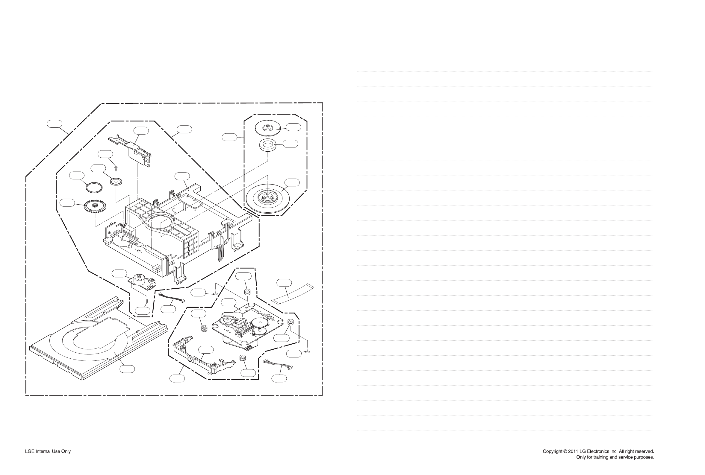
2. MECHANISM DECK SECTION (CDM-345)
MEMO
A26
01
1
2
0
01
A
1
0
A
0
02
A
01 2
2
43
6
03
6
01
2
8
01
9
43
4
01
3
01
7
5
01
43 1
00
2
00
3
00
10
0
02
A
01 2
9
01
6
3
0
A
01
2
03
2
43
7
6-25-2
Page 16
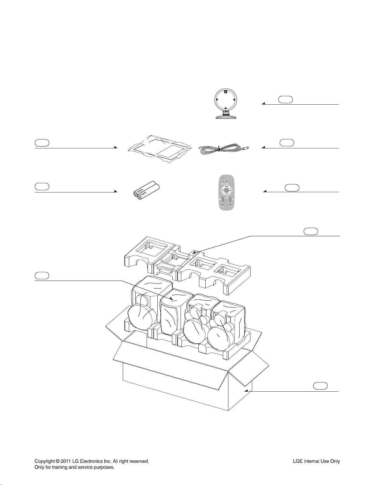
3. PACKING ACCESSORY SECTION
824 AM Loop Antenna
801 Instruction Ass'y
808 Battery
804 Bag
825 FM Wire Antenna
900 Remote Control
803 Packing
2-7
802 Box
Page 17
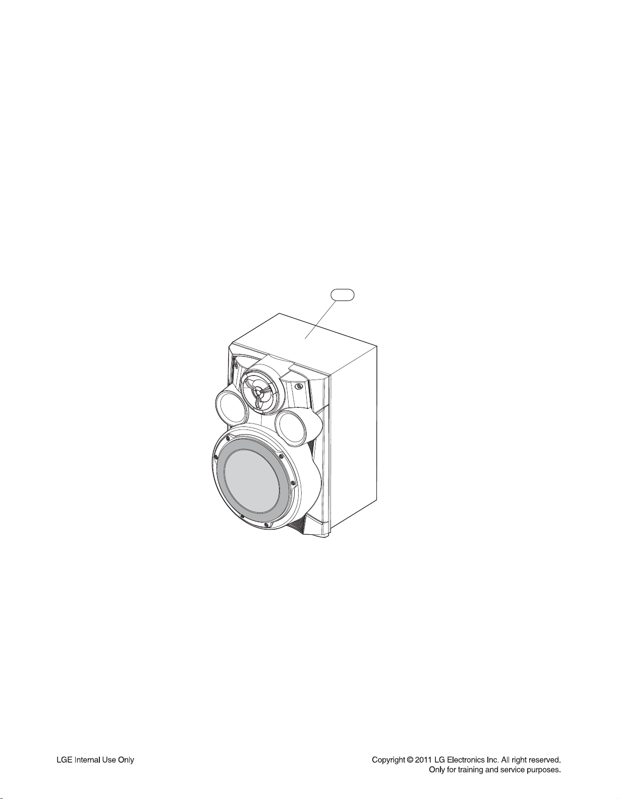
4. SPEAKER SECTION
4-1. FRONT SPEAKER (RAS376BF)
A60
2-8
Page 18
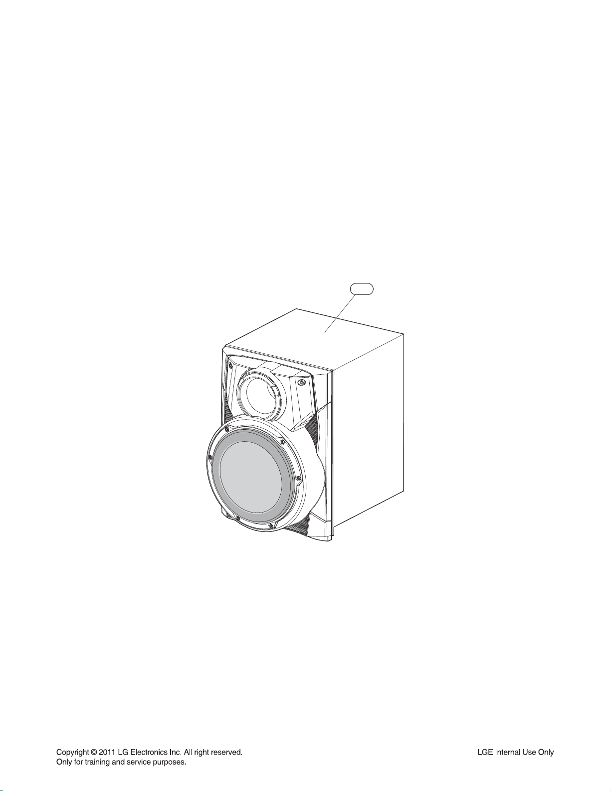
4-2. PASSIVE SUBWOOFER (RAS376BW)
A90
2-9
Page 19

MEMO
2-10
Page 20

SECTION 3
ELECTRICAL
CONTENTS
ONE POINT REPAIR GUIDE ................................................................................................................... 3-2
1. NO POWER ............................................................................................................................................ 3-2
2. NO BOOTING WHEN POWER ON THE SET ....................................................................................... 3-4
3. VFD IS NOT DISPLAYED WHEN POWER ON THE SET ..................................................................... 3-5
4. NO OPERATION OF MD ....................................................................................................................... 3-6
5. NO SOUND .......................................................................................................................................... 3-11
AUDIO ELECTRICAL TROUBLESHOOTING GUIDE .................................................................. 3-16
1. POWER (SMPS) ................................................................................................................................... 3-16
2. μ-COM PART CHECK .......................................................................................................................... 3-20
3. IC101(S24CS16A01) CHECK .............................................................................................................. 3-20
4. FLD DISPLAY CHECK ......................................................................................................................... 3-21
5. PWM MODULATION CHECK .............................................................................................................. 3-22
6. POWER AMP PART CHECK ............................................................................................................... 3-24
7. TUNER / AUX FUNCTION CHECK ...................................................................................................... 3-25
8. TUNER FUNCTION CHECK ................................................................................................................ 3-26
CDP ELECTRICAL TROUBLESHOOTING GUIDE ....................................................................... 3-27
1. CD FUNCTION ..................................................................................................................................... 3-27
2. USB FUNCTION ................................................................................................................................... 3-28
WAVEFORMS ............................................................................................................................................. 3-29
WIRING DIAGRAM ................................................................................................................................... 3-33
BLOCK DIAGRAMS ................................................................................................................................. 3-35
1. OVERALL BLOCK DIAGRAM .............................................................................................................. 3-35
2. SMPS BLOCK DIAGRAM..................................................................................................................... 3-37
CIRCUIT DIAGRAMS ............................................................................................................................... 3-39
1. SMPS CIRCUIT DIAGRAM .................................................................................................................. 3-39
2. MICOM & AD CIRCUIT DIAGRAM ...................................................................................................... 3-41
3. PWM & AMP CIRCUIT DIAGRAM ....................................................................................................... 3-43
4. CD DSP & SERVO CIRCUIT DIAGRAM ............................................................................................. 3-45
5. FRONT CIRCUIT DIAGRAM ................................................................................................................ 3-47
6. USB CIRCUIT DIAGRAM ..................................................................................................................... 3-49
CIRCUIT VOLTAGE CHART ................................................................................................................. 3-51
PRINTED CIRCUIT BOARD DIAGRAMS ......................................................................................... 3-55
1. MAIN P.C.BOARD ................................................................................................................................ 3-55
2. SMPS P.C.BOARD ............................................................................................................................... 3-59
3. FRONT P.C.BOARD ............................................................................................................................. 3-60
4. USB P.C.BOARD .................................................................................................................................. 3-61
3-1
Page 21
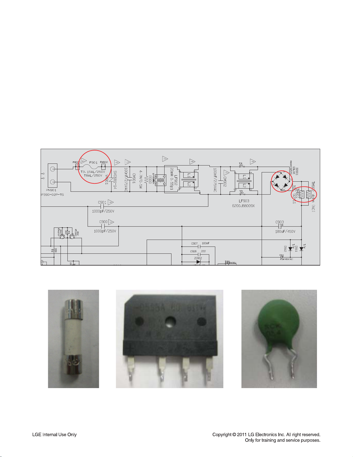
ONE POINT REPAIR GUIDE
1. NO POWER
If the unit doesn’t work by no power problem, repair the set according to the following
guide.
1-1. FUSE & BRIDGE DIODE
1-1-1. Solution
Please check and replace F901, BD901, TH901 on SMPS board.
1-1-2. How to troubleshoot (Countermeasure)
1) Check if the fuse F901 is open or short-circuit.
2) Check if the bridge diode DB901 is short-circuit by over current with a digital multi meter.
3) Check if the NTC thermistor TH901 is normal or open.
1-1-3. Service hint (Any picture / Remark)
< F901 >
If F901 is not short-circuit,
replace it with a same
specifi cations one.
replace it with a new one.
< BD901 >
If BD901 is short-circuit,
< TH901 >
If TH901 is open,
replace it with a new one.
3-2
Page 22

ONE POINT REPAIR GUIDE
NO POWER
If the unit doesn’t work by no power problem, repair the set according to the following
guide.
1-2. D929
1-2-1. Solution
Please check and replace D929 on SMPS board.
1-2-2. How to troubleshoot (Countermeasure)
1) Check the Anode-Cathod Voltage of D929 with a digital multi-meter, it is normally 0.2 ~ 0.3 V.
If it doesn’t have any voltage, it’s destroyed. Replace it with a new one.
1-2-3. Service hint (Any picture / Remark)
< SMPS schematic diagram >
3-3
Page 23

ONE POINT REPAIR GUIDE
2. NO BOOTING WHEN POWER ON THE SET
The set doesn’t work when press the power button on the front board or the remote
control.
2-1. FLASH MEMORY
2-1-1. Solution
Please check and replace IC101 on MAIN board.
2-1-2. How to troubleshoot (Countermeasure)
1) Check 3.7 V to CN304 and CN105 in standby mode.
If there is no 3.7 V, check the SMPS.
2) Check 5.6 V, 12 V, F+, F- and PVDD when power on the set.
- If the set doesn’t work regardless of what the KEY1 changes high to low while pressing the power button
X101 and X102 work normally but, if you can not power on the set, replace IC101 with a new one on
the MAIN board.
2-1-3. Service hint (Any picture / Remark)
XWX
OZYU^]_ro¡P
.
rlX
O]WP
w~ yj{ys
OyXX`P
XWY
O`U_ZW[to¡P
pjXWY
< Signal check point >
3-4
Page 24

ONE POINT REPAIR GUIDE
3. VFD IS NOT DISPLAYED WHEN POWER ON THE SET
When power on the set, any icons or characters on VFD are not displayed.
3-1. VFD
3-1-1. Solution
Please check and replace DIG502 on FRONT board.
3-1-2. How to troubleshoot (Countermeasure)
1) Check if VKK, FL+ and FL- are output from SMPS to VFD via the MAIN board.
2) Check if IC102 outputs VFD_D0, VFD_CLK and VFD_STB to the FRONT board.
3) Check the GR signal(pulse signal) of IC501 on the FRONT board.
Check the SG signal(pulse signal) of IC501 on the FRONT board.
If the GR and SG signal isn’t output, replace IC501 with a new one.
If the GR and SG signal is output, replace DIG502 with a new one.
3-1-3. Service hint (Any picture / Remark)
nyG
znG
jGGSGGGGG
GU
GG GGU
nyG
hGZWG
yZY^O{wZW[P
znG
hGZWG
3-5
< Waveform of GR and SG signal >
Page 25

ONE POINT REPAIR GUIDE
4. NO OPERATION OF MD
When no sound output in the CD function, you can not listen to music reading data
from a CD disc if the servo motors in MD don’t work. This step is for checking the
SPINDLE MOTOR among them.
4-1. SPINDLE MOTOR
4-1-1. Solution
Please check and replace IC301, IC302 on MAIN board.
4-1-2. How to troubleshoot (Countermeasure)
1) Check the SPDO signal from pin16 of IC302.
If no signal, check 3.3 V(RF) and X301.
2) Check the SPIN- & SPIN+ from IC301 to CN303 for driving SPINDLE motor. It is about 3.6 Vp-p.
If no signal, check +1.8 V and +5 V for IC301.
3) Check if the FFC cable is solidly connected between CN303 and MD.
4) Check the MD.
If the spindle motor is sort-circuit or has any trouble, it can not rotate CD discs.
Please check the function after changing another MD.
4-1-3. Service hint (Any picture / Remark)
G
ZU]} T
zwTGjuZWZ
zwRGGjuZWZ
< Waveform of SP- & SP+
for driving SPINDLE motor >
zwT
] GjuZWZ
pjZWX
zwR
\ GjuZWZ
< Signal check point >
3-6
Page 26

ONE POINT REPAIR GUIDE
NO OPERATION OF MD
When no sound output in the CD function, you can not listen to music reading data
from a CD disc if the servo motors in MD don’t work. This step is for checking the
SLED MOTOR among them.
4-2. SLED MOTOR
4-2-1. Solution
Please check and replace IC301, IC302 on MAIN board.
4-2-2. How to troubleshoot (Countermeasure)
1) Check the SLDO signal from Pin15 of IC302.
If no signal, check 3.3 V(RF) and X301.
2) Check the SLED+ & SLED- from IC301 to CN303 for driving SPINDLE motor. It is about 2.9 Vp-p.
If no signal, check +1.8 V and +5 V for IC301.
3) Check if the FFC cable is solidly connected between CN303 and MD.
4) Check the MD.
If the sled motor is sort-circuit or has any trouble, it can not move the pickup module.
Please check the function after changing another MD.
4-2-3. Service hint (Any picture / Remark)
hG
YU`} T
zsTGjuZWZ
zwT G ju[W\
zsRGGjuZWZ
zwRGGju[W\
< Waveform of SLED- & SLED+
for driving SLED motor >
zsR
Z GjuZWZ
pjZWX
zsT
[ GjuZWZ
< Signal check point >
3-7
Page 27

ONE POINT REPAIR GUIDE
NO OPERATION OF MD
When no sound output in the CD function, you can not listen to music reading data
from a CD disc if the servo motors in MD don’t work. This step is for checking the
TRAY OPEN / CLOSE MOTOR among them.
4-3. TRAY OPEN / CLOSE MOTOR
4-3-1. Solution
Please check and replace IC301, IC302 on MAIN board.
4-3-2. How to troubleshoot (Countermeasure)
1) Check MOT_OPEN & MOT_CLOSE signals from Pin104, 105 of IC801 to IC301.
If no signal, check +1.8 V & + 5 V to IC301.
2) Check LOAD± from IC301 to CN303 for driving the tray open / close motor. It is about 3.85 Vp-p.
If no signal, check +5 V to IC301. If it has any trouble, replace it with a new one.
3) Check if the FFC cable is solidly connected between CN303 and MD.
4) Check the MD.
If the tray motor is sort-circuit or has any trouble, it can not open or close the tray.
Please check the function after changing another MD.
4-3-3. Service hint (Any picture / Remark)
hG
ZU_\} T
tv{ vwlu
tv{ jsvzl
svT GjuZWZ
svRGGjuZWZ
< Waveform
for driving TRAY open / close motor >
tv{jsvzl
]GGpjZWX
tv{vwlu
^GGpjZWX
pjZWX
svT
[ GjuZWY
< Signal check point >
svR
\ GjuZWY
3-8
Page 28

ONE POINT REPAIR GUIDE
NO OPERATION OF MD
When no sound output in the CD function, you can not listen to music reading data
from a CD disc if the pickup module in MD doesn’t work. This step is for checking the
LASER TRACKING ACTUATOR.
4-4. LASER TRACKING ACTUATOR
4-4-1. Solution
Please check and replace IC301, IC302 on MAIN board.
4-4-2. How to troubleshoot (Countermeasure)
The tracking actuator makes the laser beam be positioned in the center of a track on CD disc.
1) Check the TRD signal from Pin14 of IC302.
If no signal, check 3.3 V(RF) and X301.
2) Check TR- & TR+ from IC301 to CN301 for driving the tracking actuator.
If no signal, check +1.8 V and +5 V for IC301.
3) Check if the FFC cable is solidly connected between CN301 and MD.
4) Check the MD.
If the pickup module has any trouble, it can not move the laser beam on the left or right side.
Please check the function after changing another MD.
4-4-3. Service hint (Any picture / Remark)
{yTGjuZWX
{yRGGjuZWX
< Waveform of TR±
for driving TRACKING actuator >
{T
X\ GjuZWX
pjZWX
{R
X[ GjuZWX
< Signal check point >
3-9
Page 29

ONE POINT REPAIR GUIDE
NO OPERATION OF MD
When no sound output in the CD function, you can not listen to music reading data
from a CD disc if the pickup module in MD doesn’t work. This step is for checking the
LASER FOCUSING ACTUATOR.
4-5. LASER FOCUSING ACTUATOR
4-5-1. Solution
Please check and replace IC301, IC302 on MAIN board.
4-5-2. How to troubleshoot (Countermeasure)
The focusing actuator makes the laser beam keep a regular interval with the surface of a CD disc.
1) Check the FOD signal from Pin13 of IC302.
If no signal, check 3.3 V(RF) and X301.
2) Check F- & F+ from IC301 to CN301 for driving the focusing actuator.
If no signal, check +1.8 V and +5 V for IC301.
3) Check if the FFC cable is solidly connected between CN301 and MD.
4) Check the MD.
If the pickup module has any trouble, it can not move the laser beam on the top or bottom side.
Please check the function after changing another MD.
4-5-3. Service hint (Any picture / Remark)
{T
mRGGjuZWX
mTGjuZWX
< Waveform of TR±
for driving FOCUSING actuator >
mR
XZ GjuZWX
pjZWX
mT
X] GjuZWX
< Signal check point >
3-10
Page 30

ONE POINT REPAIR GUIDE
5. NO SOUND
There is no sound output in the CD FUNCTION, repair the set according to the following guide.
5-1. IN THE CD FUNCTION
5-1-1. Solution
Please check and replace IC602, IC801 on MAIN board.
5-1-2. How to troubleshoot (Countermeasure)
1) Check CD_BCK, CD_LRCK, & CD_DATA signals from IC302 to IC801.
If no signal, check if the RF & servo signals from MD is entered to IC302.
Refer to the “No operation of MD” guide on Item 4.
2) Check the following I2S signal flow. < I2S audio signal Interface >
- DAC_BCK: IC801_Pin87 --> IC602_Pin4
- DAC_LRCK : IC801_Pin88 --> IC602_Pin5 (44.1 kHz)
- DAC_DATA : IC801_Pin83 --> IC602_Pin6,9
- DAC_MCLK : IC801_Pin86 --> IC401_Pin44
If there is any trouble, check the power for each IC. The power is normal but, if the signal waveform to
the IC is distorted or no signal, replace it with a new one.
3) Check if “Digital audio AMP block” on Item 5-2 is normal.
5-1-3. Service hint (Any picture / Remark)
{T
P/UP
DAC-BCK/LRCK/MCLK/DATA
< I2S Signal Flow >
BU9543KV
RF+ SERVO DSP
MLC9800
MCS LOGIC
PWM
PS9850
Or PS9851
khjtjsrGOX]U`Zto¡P
khjijrGOXU[to¡ P
khjkh{h
khjsyjrGO[[UXro¡ P
< Waveform of I2S audio interface signals >
3-11
Page 31

ONE POINT REPAIR GUIDE
NO SOUND
There is no sound output by DIGITAL AUDIO AMP DAMAGE, repair the set according
to the following guide.
5-2. BY DIGITAL AUDIO AMP DAMAGE (IN ALL FUNCTIONS)
5-2-1. Solution
Please check and replace IC700, IC701(Only RAT376) on MAIN board.
5-2-2. How to troubleshoot (Countermeasure)
1) Check FL±, FR± & SW± signals from IC602 to IC700 & 701 each input function.
If no signal, check if I2S audio signals are entered to IC602.
Refer to “I2S audio signal interface” on Item 5-1.
2) Check PVDD.
If PVDD is abnormal, check the SMPS.
3) Check +12 V for driving the gate of AMP IC.
a. All the powers are normal, but if +12 V is low, there is possible for AMP IC to be damaged.
b. Remove L711, L712, L713 and L714 one by one.
When removed a inductance, if +12 V is recovered, AMP IC connected to it was damaged.
c. Replace AMP IC with a new one.
4) Check the impedance between IC700/IC701_OUT-A/OUT-B & GND.
a. If the impedance is 0 Ω, AMP IC must be damaged.
b. After removing the heat sink, replace it with a new one.
5-2-3. Service hint (Any picture / Remark)
pj^WW
pj^WX
mySG ms
z~
< Signal check point >
3-12
Page 32

ONE POINT REPAIR GUIDE
NO SOUND
There is no sound output in the USB FUNCTION, repair the set according to the following guide.
5-3. IN THE USB FUNCTION
5-3-1. Solution
Please check and replace IC801 on MAIN board & IC505 on USB board.
5-3-2. How to troubleshoot (Countermeasure)
1) Check +5VU to USB board.
If the USB LED are turned on, the voltage is okay, if so not, check +5.6 V to pin4 of CN501.
2) Check USB D± from MAIN board to USB board.
a. Check USB_DN/DP signals to IC801(pin116, 117).
b. Check USB± signals from IC504 to CN501 (pin2, 3).
If there is any trouble, check the power for each IC. The power is normal but , if the signal waveform to
the IC is distorted or no signal, replace it with a new one.
3) Check if “Digital audio AMP block” on item 5-2 is normal.
5-3-3. Service hint (Any picture / Remark)
USB CON
REG IC
D+/-
IC801
MLC9800
USB
P-CTRL
DAC_DAT A
DAC_L RCK
DAC_BC K
DAC_MCLK
IC602
PS9850
PWM
< USB function signal fl ow >
AMP IC
TAS5612
kT GZ Gju[WX
kRGGGY Gju[WX
< Waveform of USB D± signal >
3-13
Page 33

ONE POINT REPAIR GUIDE
NO SOUND
There is no sound output in the AUX FUNCTION, repair the set according to the following guide.
5-4. IN THE AUX FUNCTION
5-4-1. Solution
Please check and replace IC401 on MAIN board.
5-4-2. How to troubleshoot (Countermeasure)
1) Check AUX_L/R signals to IC401 (Pin7, 8).
2) Check if DAC_BCK, DAC_LRCK, & DAC_MCLK are entered from IC801 to IC401.
3) Check if ADC_DATA is entered from IC401 to IC801.
If no signal, check +5 V & +3.3 V(ADC) for IC401. If is NG, replace it a new one.
4) Check the following I2S signal flow from IC801 to IC602. (Refer to Item 5-1.)
If there is any trouble, check the power for each IC. The power is normal but, if the signal waveform to
the IC is distorted or no signal, replace it with a new one.
5) Check if the digital audio AMP block is okay. Refer to “Digital Audio AMP” guide on Item 5-2.
If AMP is damaged, replace it with a new one.
5-4-3. Service hint (Any picture / Remark)
{T
{T
AUX_ L/R
ADC_D ATADAC_MCLK
DAC_BCK
DAC_L RCK
DAC_DATA
DAC_MCLK
IC401
CS5346
IC801
MLC9800
< AUX function signal fl ow >
AUX
IC602
PS9850
PWM
AMP IC
TAS5612
h kjk h{hGG Gy[W`
khjijr Gy[W_
khjsyjr Gy[W^
khjtjsr Gy[W]
h| sGGy[Y\ h|yGGy[Y[
< Signal check point >
3-14
Page 34

ONE POINT REPAIR GUIDE
NO SOUND
There is no sound output in the TUNER FUNCTION, repair the set according to the
following guide.
5-5. IN THE TUNER FUNCTION
5-5-1. Solution
Please check and replace IC401, TU100 on MAIN board.
5-5-2. How to troubleshoot (Countermeasure)
1) Check if TUNER_LR is entered from Pin1,3 of TU100 to IC401(Pin23, 24).
If no signals, Check +3.3 V for Tuner power.
Check if the Tuner control signals (CLK, DAT, CE, RST, SLT) are entered from IC102 to TU100.
If it doesn’t work, replace TUNER with a new one.
2) Check if DAC_BCK, DAC_LRCK, & DAC_MCLK are entered from IC501 to IC202.
3) Check if ADC_DATA is entered from IC401 to IC801.
If no signal, check +5 V & +3.3 V(ADC) for IC401. If is NG, replace it a new one.
4) Check the following I2S audio signal flow from IC801 to IC602. (Refer to Item 5-1.)
If there is any trouble, check the power for each IC. The power is normal but, if the signal waveform to
the IC is distorted or no signal, replace it with a new one.
5) Check if the digital audio AMP block is okay. Refer to “Digital Audio AMP” guide on Item 5-2.
If AMP is damaged, replace it with a new one.
5-5-3. Service hint (Any picture / Remark)
{T
IC401
{T
CS5346
IC801
MLC9800
< TUNER IN function signal fl ow >
TUNER _L/R
ADC_D ATADAC_MCLK
DAC_BCK
DAC_L RCK
DAC_DATA
DAC_MCLK
IC602
PS9850
PWM
TUNER
AMP IC
TAS5612
h kjk h{hGG Gy[W`
khjijr Gy[W_
khjsyjr Gy[W^
khjtjsr Gy[W]
< Signal check point >
{| uly y Gj[ZW
{| uly s Gj[Y`
3-15
Page 35

AUDIO ELECTRICAL TROUBLESHOOTIHG GUIDE
1. POWER (SMPS)
No 3.7 VA
YES
Is F901 normal? Replace F901 (Use the same fuse).
YES
Is BD901 normal? Replace BD901.
YES
Is TH901 normal? Replace TH901.
YES
Is Vcc
(10 V ~ 18 V) supplied to
IC901 Pin7?
NO
NO
NO
NO
Is D904 normal?
NO
YES
Is D922 normal? Replace D922.
YES
Is there
about 2.5 V at
IC903 Pin1?
YES
Is D923 normal? Replace D923.
YES
Is D921 normal? Replace D921.
YES
Is D924 normal? Replace D924.
YES
Is D925 normal? Replace D925.
YES
Power line of I/O PCB is short.
NO
NO
NO
NO
NO
NO
Check or replace D904.
Replace IC903.
3-16
Page 36

AUDIO ELECTRICAL TROUBLESHOOTIHG GUIDE
No PVDD
YES
Is F901 normal? Replace F901 (Use the same fuse).
YES
Is BD901 normal? Replace BD901.
YES
Is TH901 normal? Replace TH901.
NO
NO
NO
Is Vcc
(10 V ~ 18 V) supplied to
IC902 Pin7?
YES
NO
Is D905 normal?
YES
Is Q910 base "H"?
YES
•
Check P-CTRL "H" signal from μ-COM. •
Check PC902.
Check or replace Q910.
Is Q902 normal? Replace Q902.
YES
Is D929 normal? Replace D929.
YES
Is there about 2.5 V
at IC904 Pin1?
NO
NO
NO
Replace IC904.
NO
Check or replace D905.
NO
YES
Power line of main PCB is short.
3-17
Page 37

AUDIO ELECTRICAL TROUBLESHOOTIHG GUIDE
No 12 V
YES
Is Vcc
(15 V) supplied to Q953
collector?
YES
Is the
13 V Supplied to Q953
base?
YES
Check or replace Q953.
No 5 V
YES
Is Vcc
(6 V) supplied to IC951
Pin1?
NO
NO
NO
Check or replace D921.
Check P-CTRL “H” signal
from μ-COM.
Check or replace D923.
YES
Check
IC951 Pin4 "H".
YES
Check or replace IC951.
NO
Check P-CTRL
“H”’ signal from μ-COM.
3-18
Page 38

AUDIO ELECTRICAL TROUBLESHOOTIHG GUIDE
No VFD
YES
Is D925 normal?
YES
Is ZD951 normal?
YES
Is Q951 normal?
YES
Check or replace VFD.
NO
NO
NO
Check or replace D925.
Check or replace ZD951.
Check or replace Q951.
3-19
Page 39

AUDIO ELECTRICAL TROUBLESHOOTIHG GUIDE
2. μ-COM PART CHECK
μ-COM PART
CHECK
YES
Check if
voltage of CN105 Pin10
is 3.7 VA.
YES
Check
both end voltage of
D102, D105.
YES
Check if IC102_Pin49 and
IC102_Pin36,59 are 3.5 V.
YES
X101:32.768kHz
X102:9.8304MHz
Check the operation.
YES
OK
NO
NO
Refer to
SMPS troubleshooting.
Check if output of
D105(MBR0540) is 3.7 V.
Check D102, D105.
YES
OK
NONO
Replace D102, D105.
3. IC101(S24CS16A01) CHECK
CHECK
IC102 PIN47,48
YES
Pin47: DATA
Pin48: CLK.
YES
OK OK
NO
Check μ-COM
voltage 3.5 V.
YES
Check μ-COM.
YES
3-20
NO
Refer to μ-COM troubleshooting.
NO
Replace μ-COM.
Page 40

AUDIO ELECTRICAL TROUBLESHOOTIHG GUIDE
4. FLD DISPLAY CHECK
FLD DISPLAY CHECK
YES
Check
CN104 Pin1,2,3 input
voltage.
YES
Check if both end voltage
of F1,F2 are over 3.4 V
VKK : over 26 V.
YES
Check CN304
connection and power
Pin14,15,16(VKK,FL-,FL+),
Pin11(3.7 VA).
YES
Check
IC501(ET6315) voltage
Pin30 VKK:-26 V
Pin13, 43:+5 V.
NO
Refer to SMPS troubleshooting.
NO
Check CN304 connection.
YES
Check each
Pin voltage.
YES
OK
NO
If voltage is Not 3.7 VA,
check input and output of D501.
YES
YES
Check
IC102->IC501
data communication
Pin3->Pin9 STB
Pin2->Pin7 DATA
Pin4->Pin8 CLK
YES
FLD light on?
YES
OK
Check IC501.
YES
OK
NO
Check output data IC102 Pin2.
Check input data
IC102 Pin2,3,4.
YES
YES
Check IC102.
YES
OK
3-21
NO
Replace IC501.
NO
Replace IC102.
Page 41

AUDIO ELECTRICAL TROUBLESHOOTIHG GUIDE
5. PWM MODULATION CHECK
PWM MODULATION PART CHECK
YES
Check
CN105 Pin10 3.7 VA.
YES
• Check IC602(PS9850) VDD 3.3 V
(Pin16,24,29,32,35,40,48,61,64)
• Check VDD Core 1.2 V (Pin1,21,43,57,59,60)
• Check X602(19.2 MHz)
YES
Check
X602(19.2 MHz)
operation.
YES
Check
IC602(PS9850)
Pin51 CLK input.
NO
SMPS troubleshooting.
NO
Refer to
Check X602
(19.2 MHz).
YES
OK
NO
Replace X602(19.2 MHz).
YES
Check
IC102(LC87Fxx)
Pin41:PWM RESET
Pin45:PWM SDA
Pin46:PWM SCL
output.
YES
A
NO
Check line
resistor output
RST: R636 / SCL: R637 /
SDA: R638.
YES
OK
3-22
NO
Replace R636,R637,R638.
Page 42

AUDIO ELECTRICAL TROUBLESHOOTIHG GUIDE
A
YES
Check
IC602(PS9850)
input data
Pin4, 5, 6
PWM wave.
YES
Check
PWM
modulator output
FL: Pin31(+),30(-)
FR: Pin28(+),27(-)
and others.
NO
NO
Check
CD Assy communication
Pin4, 5, 6.
YES
Check
IC602(PS9850) input
data.
YES
OK
Check
IC602(PS9850).
YES
NO
NO
NO
Refer to
CD troubleshooting.
Check each line
resistor output.
Replace
IC602(PS9850).
OK
YES
OK
3-23
Page 43

AUDIO ELECTRICAL TROUBLESHOOTIHG GUIDE
6. POWER AMP PART CHECK
POWER AMP PART CHECK
YES
Check
CN105 Pin2: +12 V
Pin13,15: 29 V.
YES
Check IC700, IC701
Pin30,31,38,39,42,43,50,51 input voltage.
YES
Check each IC603
Pin64:+12 V input.
YES
Check PWM Modulator input
IC700 Pin4,5,10,11 / IC701 Pin4, 5.
YES
Check IC701, IC702
Pin28,29,36,37,43,44,52,53.
NO
Refer to SMPS troubleshooting.
NO
Check each line resistor output voltage.
YES
Check output
line coil.
YES
OK
NO
Replace the coil.
3-24
Page 44

AUDIO ELECTRICAL TROUBLESHOOTIHG GUIDE
7. TUNER / AUX FUNCTION CHECK
FUNCTION CHECK
YES
Check IC401
(CS5346) Pin7,8,
23,24 input.
YES
Check IC401
(CS5346) Pin9 output
data.
YES
Check
IC801(MLC9800)
input data.
YES
IC501(MLC9800)
output data.
NO
Check JK401,TU100.
Check IC401
Pin5: +5 V
Pin46: +3.3 V.
YES
Check IC401
Pin5: +5 V,
Pin6: High,
Pin46: 3.3 V.
NONO
NONO
Check CN105 Pin7: +5 V
Pin9,10: +3.3 V.
Check IC401
Pin41: SDOUT,
Pin42: SLCK,
Pin43: LRCK,
Pin44: MCLK.
OK
YES
3-25
Page 45

AUDIO ELECTRICAL TROUBLESHOOTIHG GUIDE
8. TUNER FUNCTION CHECK
TUNER FUNCTION CHECK
YES
Check tuner
module(TU100)
operation.
YES
Check IC102 Pin21, 22, 23, 24, 25
data in/output.
YES
Refer to function check.
NO
NO
Check tuner module voltage
(Pin4: +3.3 V).
Check tuner module data.
3-26
Page 46

CDP ELECTRICAL TROUBLESHOOTIHG GUIDE
1. CD FUNCTION
CD FUNCTION
YES
Can the
disc insert?
YES
Disc reading
is ok?
YES
Is no signal at spk?
YES
Check
the signal of
IC302 Pin34,35,36.
NO
Is load +,- ok?
Is Motor ok?
(about 12 Ω)
NO
OPU driving (Focus
and tracking) is ok?
NO
Check Vcc of IC302.
YES
NO
NO
NO
Is Motor_open/close
OK? (IC301 Pin10,11)
Check IC301.
Check loading motor.
Focus/
tracking/sled signal
Is the PD(CN301
Pin12) about 180mV?
YES
is ok?
YES
NO
NO
Check IC301
(Motor drive IC).
Check OPU
(pick-up).
YES
Check
the signal (16.0344 MHz)
of IC302
Pin31.
YES
Check IC801
input/output and
control line.
YES
Refer to function
check.
NO
NO
Check Cristal (X301).
Replace IC801.
NO
3-27
Replace Cristal
(X301).
Page 47

CDP ELECTRICAL TROUBLESHOOTIHG GUIDE
2. USB FUNCTION
USB FUNCTION
YES
Plug-in usb device.
YES
Display “NO USB”.
YES
Display “READ”.
YES
Display “NO FILE”.
YES
Check usb audio fi le in usb device
(MP3, WMA fi le is playable)
Check USB_5V.
YES
Check USB_D+/D-
(R501,R502).
YES
Check IC801(Pin116, 117).
NONO
Check CN401.
NO
Check usb jack (JK501).
NO
Replace IC801.
3-28
Page 48

1. SDRAM
WAVEFORMS
2. SERVO
CLK
1
DATA
2
ADDRESS
3
CS
4
IC802 Pin38
IC802 Pin53
IC802 Pin35
IC803 Pin1
5
IC801 Pin63
CD-16M
3-29
Page 49

6
IC302 Pin61
TE
FE
7
IC302 Pin62
FOD
8
IC302 Pin13
RF
9
3. AUDIO PATH
10
IC302 Pin63
IC801 Pin100
CD_BCK
11
12
3-30
CD_LRCK
CD_DATA
IC801 Pin102
IC801 Pin101
Page 50

13
14
DAC_MCK
IC801 Pin86
DAC_BCK
IC801 Pin87
4. USB
15
16
USB_5V
DAC_LRCK
DAC_DATA
IC801 Pin88
IC801 Pin83
17
18
D+
D-
IC801 Pin116
IC801 Pin117
3-31
Page 51

MEMO
3-32
Page 52

WIRING DIAGRAM
(CDM-345)
CN901
CN902
CN903
6PIN
CN105
CN401
CN301
CN104
CN303
CN302
CN304
CN502
CN501
3-33 3-34
Page 53

BLOCK DIAGRAMS
s
s,Ts
s
s
1. OVERALL BLOCK DIAGRAM
DECK MECHANISM
P/UP
M
SLED
SPINDLE
A,B,C,D,E,F
,F
s
LOAD
PD
LD
AM5890S
MOTOR
IC
FDO
TDO
SLDO
SPDO
OP/CL
16.93MHZ
BU9543KV
RF+ SERVO DSP
9543-RST;
DAC-MCLK
CD_DIN_DOUT
CD_MCK/ CD_R/W
CD-BCK/ LRCK/ DOUTA
BUSY; CD-16M
SUBSYQ;
DAC-BCK/LRCK/MCLK
DAC-DATA
SPI-DO/DI/CLK/ CS
12.288MHZ
PWM
PS9850
PWM-RST
PWM-CLK
L
FL+
FL-
FR+
AMP
TAS5612
R
FR-
PWM-DAT
SD; OTW
PDN
9.8304MHZ
EEPROM
DAT
CLK
SDRAM
EM638165TS-6G
FLASH
MX25LB005BMC
RESET; MU
TE
OP/CL LI MIT
DSCK#,CKE,CS0#,RAS0#
DMA[0..11],DB[0..15]
A[0.. 18], DB[0..15]
RST, WEN#,CE#
12MHZ
MLC9800
MCS LOGIC
P-CTRL
USB CON
REG IC
I2S CLK
CS5346
ADC(6CH)
ADC-DATA
ADC-RST
ADC-DAT
ADC-CLK
DAT, CLK, RST, CE, INT
MICOM
LC87F5M64A
32.766khz
P-SENSE
STB
R/L
R/L
CLK
DO
D+/-
VFD DRIVER
ET6315
RMC
+12V
POWER
AUX
TUNER
VFD
KEY
Standby LED
I/F
VOLUME LED
3.7V
3-35 3-36
Page 54

2. SMPS BLOCK DIAGRAM
SMPS
م
ࣧ
م
م
م
م
Snubber
Block
م
Main
SMPS IC
Block
T
R
A
N
S
م
5V LDO
12V
Regulation
Block
On/Off
م
On/Off
On/Off
FL+
FL-
Vkk
5V
5.6VA
12V
3.7VA
CN901
CN902/3
Noise
Filter
Block
(X-cap
Line Filter)
F
U
S
E
Y-Cap
Y-Cap
م
Snubber
م
AMP
SMPS IC
With FET
Block
Block
م
Photo coupler
On/Off
Photo coupler
Photo coupler
T
R
A
N
S
Feedback
Feedback
م
م
م
CD P.CTL
P. C TL
PVDD
3-37 3-38
Page 55

CIRCUIT DIAGRAMS
1. SMPS CIRCUIT DIAGRAM
12
11
10
9
8
IMPORTANT SAFETY NOTICE
WHEN SERVICING THIS CHASSIS, UNDER NO
CIRCUMSTANCES SHOULD THE ORIGINAL DESIGN BE
MODIFIED OR ALTERED WITHOUT PERMISSION
FROM THE LG CORPORATION. ALL COMPONENTS
SHOULD BE REPLACED ONLY WITH TYPES IDENTICAL
TO THOSE IN THE ORIGINAL CIRCUIT. SPECIAL
COMPONENTS ARE SHADED ON THE SCHEMATIC
FOR EASY IDENTIFICATION.
THIS CIRCUIT DIAGRAM MAY OCCASIONALLY DIFFER
FROM THE ACTUAL CIRCUIT USED. THIS WAY,
IMPLEMENTATION OF THE LATEST SAFETY AND
PERFORMANCE IMPROVEMENT CHANGES INTO
THE SET IS NOT DELAYED UNTIL THE NEW SERVICE
LITERATURE IS PRINTED.
NOTE :
1. Shaded(
2. Voltages are DC-measured with a digital voltmeter
) parts are critical for safety.
Replace only with specified part number.
during Play mode.
7
6
5
4
3
2
CAUTION:
Danger if fuse is incorrectly replaced.
1
Replace only with the type identical to fuse rating
and(or) model name described in main label.
A
B C D E F G H I J K L M N O P Q R ST
Warning
Parts that are shaded are critical with
respect to risk of fire or electrical shock.
EBY60749101 Rev 7.1
SMPS
2010.11.09
3-39 3-40
Page 56

2. MICOM & AD CIRCUIT DIAGRAM
12
11
10
9
8
7
6
5
4
3
2
1
EBY61070801(#1) Rev 1.9
A
B C D E F G H I J K L M N O P Q R ST
µ-COM & AD
2010.11.09
3-41 3-42
Page 57

3. PWM & AMP CIRCUIT DIAGRAM
12
11
10
9
8
7
6
5
4
3
2
1
EBY61070801(#2) Rev 1.9
A
B C D E F G H I J K L M N O P Q R ST
PWM & AMP
2010.11.09
3-43 3-44
Page 58

4. CD DSP & SERVO CIRCUIT DIAGRAM
12
11
10
9
7 69
5
2
8
8
16
7
13
14
1
3
15
6
5
10 12 11 17 18
4
4
3
2
1
: WAVEFORM NUMBER
A
B C D E F G H I J K L M N O P Q R ST
CD DSP & SERVO
EBY61070801(#3) Rev 1.9
2010.11.09
3-45 3-46
Page 59

5. FRONT CIRCUIT DIAGRAM
12
11
10
9
8
7
6
5
4
3
2
1
EBY61070901 Rev 2.2
A
B C D E F G H I J K L M N O P Q R ST
FRONT
2010.11.09
3-47 3-48
Page 60

6. USB CIRCUIT DIAGRAM
12
11
10
9
8
7
6
5
4
3
2
1
EBY61071001 Rev 1.5
A
B C D E F G H I J K L M N O P Q R ST
USB
2010.11.09
3-49 3-50
Page 61

CIRCUIT VOLTAGE CHART
1. SMPS Board
P.OFF(STANBY) P.ON (Unloaded) CD_PLAY (USB insert)
Location Cap Mode
3.7VA C923 330uF/16 3.70 40 3.70 200 3.70 220
5.0V(Main) C951 100uF/16 0 0 5.0 40 5.0 200
F+ - - -24 0 -19 132 -19.0 136
F- C952 - -24 0 -23.5 130 -23.5 130
VKK C926 47u/50 -26 10 -26.5 10 -26 10
12V C921 100/50 0 0 12 100 12 115
PVDD C932 1000/35 0 0 21.5 600 21.5 600
Voltage
(V)
Current
(mA)
Voltage
(V)
Current
(mA)
Voltage
(V)
2. MAIN Board
Location Pin No. Specifi cation EE Mode (V) Margin Playback Mode (V) Margin
IC101 EEPROM (M24C16)
8 (VCC) 1.8~5.5 3.4 2.1 3.4 2.1
IC102 MICOM (LC87F5M64A)
9 (VDD2) 2.8~5.5 3.4 0.6 3.4 0.6
36 (VDD3) 2.8~5.5 3.4 0.6 3.4 0.6
59(VDD1) 2.8~5.5 3.4 0.6 3.4 0.6
IC301 MOTOR IC
8 (VCC1) 4.3~13.2 4.95 0.65 4.93 0.63
19 (VCC2) 4.3~Vcc1 4.95 0.65 4.93 0.63
IC302 SERVO (BU9543KV)
1 (AVDD1) 2.7~3.6 3.24 0.36 3.24 0.36
17 (DVDD) 2.7~3.6 3.24 0.36 3.24 0.36
33 (DVDD) 2.7~3.6 3.24 0.36 3.24 0.36
26 (VDD_CORE) 1.35~1.65 1.56 0.09 1.56 0.09
37 (VDD_CORE) 1.35~1.65 1.56 0.09 1.56 0.09
47 (DVDD) 2.7~3.6 3.24 0.36 3.24 0.36
53 (DVDD2) 2.7~3.6 3.24 0.36 3.24 0.36
58 (AVDD2) 2.7~3.6 3.24 0.36 3.24 0.36
IC401 ADC (CS5346)
5 (VLC) 3.13~5.25 4.94 0.31 4.94 0.31
14 (VA) 4.75~5.25 4.94 0.31 4.94 0.31
30 (VA) 4.75~5.25 4.94 0.31 4.94 0.31
36 (VLS) 3.13~5.25 3.24 2.01 3.24 2.01
46 (VD) 3.13~3.47 3.24 0.23 3.24 0.23
IC602 PWM (PS9850)
16 (VDD_IO) 2.97~3.63 3.23 0.4 3.23 0.4
21 (VDD_CORE) 1.08~1.32 1.24 0.08 1.24 0.08
24 (VDD_IO) 2.97~3.63 3.22 0.41 3.22 0.41
29 (VDD_IO) 2.97~3.63 3.22 0.41 3.22 0.41
32 (VDD_IO) 2.97~3.63 3.22 0.41 3.22 0.41
35 (VDD_IO) 2.97~3.63 3.24 0.39 3.24 0.39
40 (VDD_IO) 2.97~3.63 3.24 0.39 3.24 0.39
Current
(mA)
Location Pin No. Specifi cation EE Mode (V) Margin Playback Mode (V) Margin
43 (VDD_CORE) 1.08~1.32 1.24 0.08 1.24 0.08
48 (VDD_IO) 2.97~3.63 3.22 0.41 3.22 0.41
57 (VDD_CORE) 1.08~1.32 1.24 0.08 1.24 0.08
59 (VDDA) 1.08~1.32 1.24 0.08 1.24 0.08
61 (VDD_VIN2) 2.20~3.30 3.22 0.08 3.22 0.08
64 (VDD_VIN1) 2.20~3.30 3.22 0.08 3.22 0.08
IC700 AMP (TAS5612)
56 (GVDD_B) 10.8~13.2 11.6 1.6 11.6 1.06
64 (VDD) 10.8~13.2 11.7 1.5 11.7 1.07
25 (GVDD_C) 10.8~13.2 11.7 1.03 11.7 1.06
26 (GVDD_D) 10.8~13.2 11.7 1.03 11.7 1.06
30 (PVDD_D) 0~34 21.5 12.1 21.5 12.1
31 (PVDD_D) 0~34 21.5 12.1 21.5 12.1
39 (PVDD_C) 0~34 21.5 12.1 21.5 12.1
42 (PVDD_B) 0~34 21.5 12.1 21.5 12.1
50 (PVDD_A) 0~34 21.5 12.1 21.5 12.1
51 (PVDD_A) 0~34 21.5 12.1 21.5 12.1
55 (GVDD_A) 10.8~13.2 11.7 1.03 11.7 1.06
IC801 (MLC9800)
2 (AVDD33) 2.97~3.63 3.2 0.43 3.2 0.43
13 (VDD12) 1.08~1.32 1.2 0.12 1.1 0.22
30 (IOVDD33) 2.97~3.63 3.2 0.43 3.2 0.43
47 (VDD12) 1.08~1.32 1.2 0.12 1.1 0.22
51 (IOVDD33) 2.97~3.63 3.2 0.43 3.2 0.43
84 (IOVDD33) 2.97~3.63 3.2 0.43 3.2 0.43
94 (VDD12) 1.08~1.32 1.2 0.12 1.2 0.12
113 (IOVDD33) 2.97~3.63 3.2 0.43 3.2 0.43
115 (USBVDD33) 2.97~3.63 3.2 0.43 3.2 0.43
120 (PLL1VDD12) 1.08~1.32 1.2 0.12 1.2 0.12
122 (PLL3VDD12) 1.08~1.32 1.2 0.12 1.2 0.12
124 (PLL2VDD12) 1.08~1.32 1.2 0.12 1.2 0.12
IC802 SDRAM
1 (VDD) 3.0~3.6 3.2 0.4 3.26 0.34
3 (VDDQ) 3.0~3.6 3.2 0.4 3.26 0.34
9 (VDDQ) 3.0~3.6 3.2 0.4 3.26 0.34
14 (VDD) 3.0~3.6 3.2 0.4 3.26 0.34
27 (VDD) 3.0~3.6 3.2 0.4 3.26 0.34
43 (VDDQ) 3.0~3.6 3.2 0.4 3.26 0.34
49 (VDDQ) 3.0~3.6 3.2 0.4 3.26 0.34
IC803 Flash
8 (VDD) 2.7~3.6 3.2 0.4 3.2 0.4
3-51 3-52
Page 62

MEMO
Location
No.
C118
C302 100uF 16V 0.22V 0V 0.22V 15.78V 3.31 0V 3.31 12.69V 3.26 0.03 3.23V 12.77V
C304 100uF 16V 0V 0V 0V 16V 1.65V 0V 1.65V 14.35V 1.64 0.03 1.61V 14.39V
C311 47uF 16V 0.22V 0.13V 0.09V 15.78V 3.17V 2.44V 0.73V 12.83V 3.1 2.37 0.73V 15.27V
C313 100nF 50V 0V 0V 0V 50V 4.97V 0V 4.97V 45.03V 4.92 0 4.92V 45.08V
C317 100uF 6.3V 0V 0V 0V 6.3V 1.57V 0V 1.57V 4.73V 1.57 0 1.57V 4.73V
C326 100uF 16V 0V 0V 0V 16V 4.97V 0V 4.97V 11.03V 4.92 0 4.92V 11.08V
C336 3.3uF 50V 0V 0V 0V 50V 1.65V 1.65V 0V 48.35V 1.65 1.64 0.01V 49.99V
C338 47uF 16V 0.22V 0V 0.22V 15.78V 3.31 0V 3.31 12.69V 3.25 0.03 3.22V 12.78V
C347 100uF 16V 0.11V 0V 0.11V 15.89V 1.65V 0V 1.65V 14.35V 1.64 0.03 1.61V 14.39V
C357 47uF 16V 0.22V 0V 0.22V 15.78V 3.31V 0V 3.31V 12.69V 3.25 0.03 3.22V 12.78V
C406 47uF 16V 0.22V 0V 0.22V 15.78V 3.31V 0V 3.31V 12.69V 3.26 0 3.26V 12.74V
C408 100uF 16V 0V 0V 0V 16V 2.49V 0V 2.49V 13.51V 0 0 0V 16V
C410 47uF 16V 0.24V 0V 0.24V 15.76V 4.97V 0V 4.97V 11.03V 3.65 0 3.65V 12.35V
C423 47uF 16V 0V 0V 0V 16V 4.02V 0V 4.02V 11.98V 1.41 0 1.41V 14.59V
C613 10uF 16V 0V 0V 0V 16V 1.25V 0V 1.25V 14.75V 1.24 0 1.24V 14.76V
C6A0 470uF 10V 0V 0V 0V 10V 1.25V 0V 1.25V 8.75V 1.24 0 1.24V 8.76V
C6A1 100pF 50V 0.18V 0V 0.18V 49.82V 1.65V 0V 1.65V 48.35V 3.25 0 3.25V 46.75V
C825 47uF 16V 0.2V 0V 0.2V 15.8V 3.31V 0V 3.31V 12.69V 3.26 0 3.26V 12.74V
C827 47uF 16V 0V 0V 0V 16V 1.19V 0V 1.19V 14.81V 1.18V 0V 1.18V 14.82V
C828 47uF 16V 0.2V 0V 0.2V 15.8V 3.31V 0V 3.31V 12.69V 3.26V 0V 3.26V 12.74V
C848 47uF 16V 0V 0V 0V 16V 1.19V 0V 1.19V 14.81V 1.18V 0V 1.18V 14.82V
C849 100nF 50V 0.22V 0V 0.22V 49.78V 3.32V 0V 3.32V 46.68V 3.26V 0V 3.26V 46.74V
C8F6 47uF 16V 0.2V 0V 0.2V 15.8V 3.31V 0V 3.31V 12.69V 3.26 0 3.26V 12.74V
C8F7 47uF 16V 0V 0V 0V 16V 1.19V 0V 1.19V 14.81V 1.18 0 1.18V 14.82V
Value
(uF)
1000uF
Spec (+) (-) Gap Margin (+) (-) Gap Margin (+) (-) Gap Margin
6.3V 3.5V 0V 3.5V 2.8V 3.44V 0V 3.44V 2.86V 3.39V 0V 3.39V 2.91V
EEMode Play back Rec voltage
3. FRONT Board
Location Pin No. Specifi cation EE Mode (V) Margin Playback Mode (V) Margin
IC501 VFD (ET6315)
13 (VDD) 4.5~5.5 3.5 -1 3.48 -1.02
43 (VDD) 4.5~5.5 3.5 -1 3.48 -1.02
30 (VEE) VDD-35 -25.8 9.2 -25.5 9.5
Location No.
Value
(uF)
Spec
(+) (-) Gap
C510 47uF 16V 3.5V 0V 3.5V 12.5V 3.5V 0V 3.5V 12.5V 3.4V 0V 3.4V 12.6V
C514 47uF 35V 0V
C516 100uF 16V 3.6V 0V 3.6V 12.4V 3.6V 0V 3.6V 12.4V 3.6V 0V 3.6V 12.4V
C549 47uF 16V 6.2V 0V 6.2V 9.8V 6.1V 0V 6.1V 9.9V 5.7V 0V 5.7V 10.3V
C551 100uF 16V 5V 0V 5V 11V 5V 0V 5V 11V 5V 0V 5V 11V
EE Mode Playback Rec voltage
-25.9V
Margin
(+) (-) Gap
25.9V 9.1V 0V -25V 25V 10V 0V
Margin
(+) (-) Gap
-24.2V
24.2V 10.8V
Margin
3-53 3-54
Page 63

PRINTED CIRCUIT BOARD DIAGRAMS
1. MAIN P.C.BOARD
(TOP VIEW)
3-55 3-56
Rev 2.2
Page 64

MAIN P.C.BOARD
(BOTTOM VIEW)
EAX63554401 Rev 2.2
3-57 3-58
Page 65

2. SMPS P.C.BOARD 3. FRONT P.C.BOARD
NOTE) Warning
Parts that are critical with respect to risk
of fire or electrical shock.
Rev 6.2
3-59 3-60
Page 66

4. USB P.C.BOARD
MEMO
3-61 3-62
Page 67

MEMO MEMO
3-63 3-64
 Loading...