
NOTE:
Active links in this document
are outlined in blue.
LG Electronics Alabama, Inc.
Plasma One Point Repair 2004
Contents
. Visual repair Index
. Introduction to Plasma
. Service Adjustments
. Trouble shooting
1
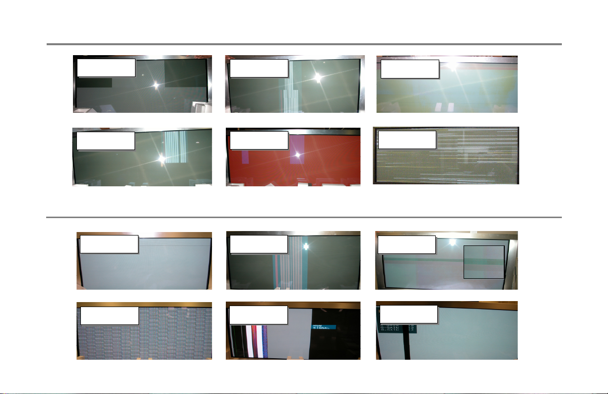
60’’ Known Visual problems with boards that fixed
Visual repair Index
Page # 37
Page # 37
Control Board & Y-Driver Amp
Page # 40
Page # 40
Y-Driver Top
Page # 38
Page # 38
Y- Amp
Page # 41
Page # 41
Control Board
60’’ Known Visual problems with boards that fixed
Page # 43
Page # 43
Y-Driver - Top
Page # 46
Page # 46
Page # 44
Page # 44
VSC- Board
Page # 47
Page # 47
Page # 39
Page # 39
Y-Driver Amp
Page # 42
Page # 42
X-Board upper right
Page # 45
Page # 45
Y-Driver - Top
Page # 48
Page # 48
VSC- Board
X- Board ( Top Right)
Y-Driver amp and X-Drive Top
2
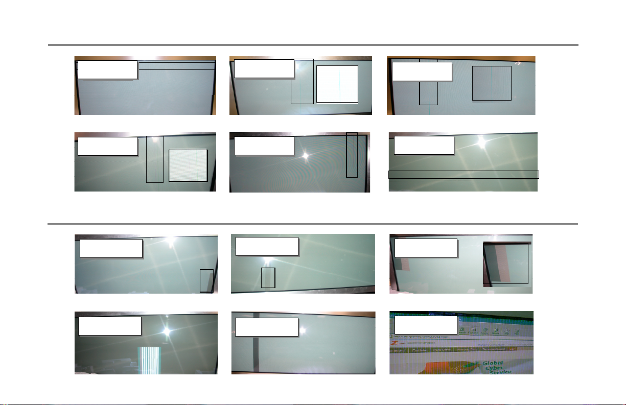
50’’ Known Visual problems with boards that fixed
Visual repair Index
Page # 49
Fig # 13
Page # 49
Fig # 13
Y-Driver Amp upper
Page # 52
Page # 52
VSC Board
Page # 50
Page # 50
Control board
Page # 53
Page # 53
X-Board upper right
50’’ Known Visual problems with boards that fixed
Page # 56
Page # 55
Page # 55
X- Board ( Lower Right)
Page # 58
Page # 58
Page # 56
X- Board ( Lower Left)
Page # 59
Page # 59
Page # 51
Page # 51
Control Board
Page # 54
Page # 54
Y- Driver Amp bottom
X- Board ( Bottom Left)
Page # 57
Page # 57
Control Board
Page # 60
Page # 60
Y- Driver Bottom
Y- Driver Amp and X-Drive Top
Control Board
3
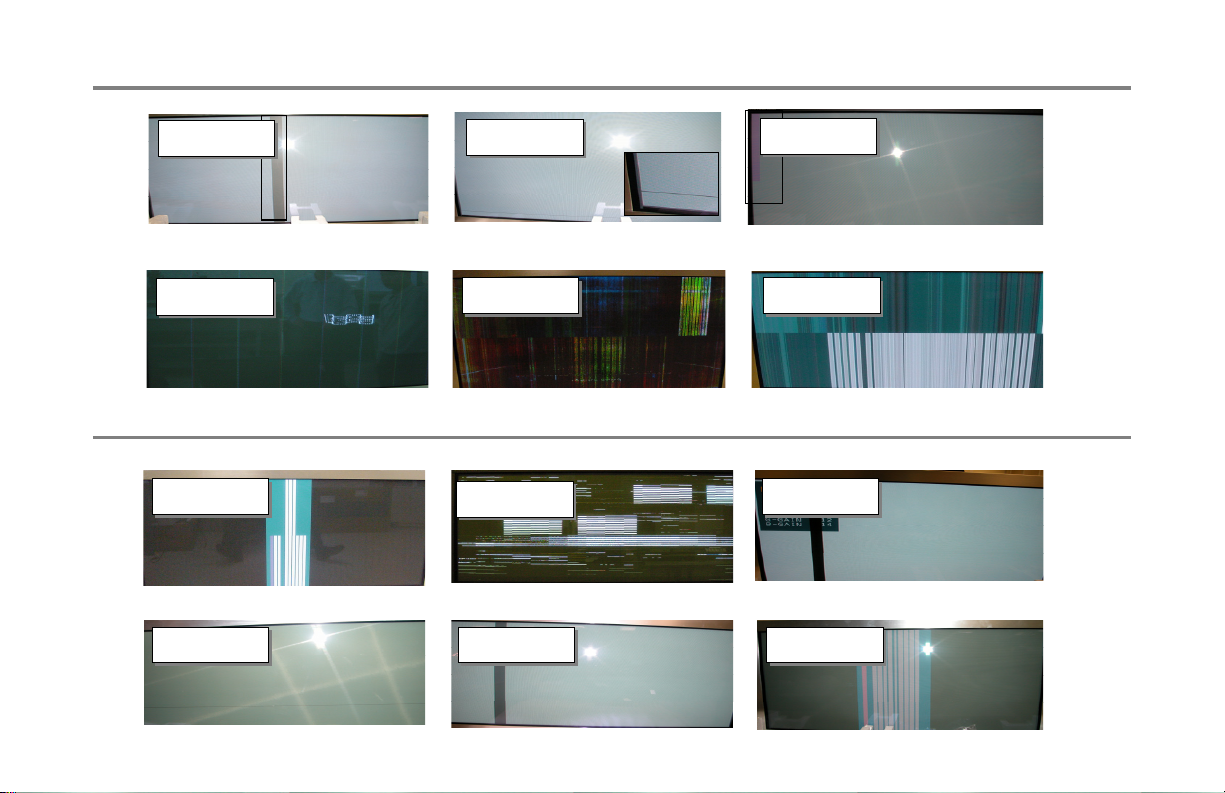
42’’ Known Visual problems with boards that fixed
Visual repair Index
Page # 61
Page # 61
Data @ X-Board – Yes/ tested for shorted
FOC IC – Ribbon shorted/ Defective Panel
Page # 64
Page # 64
Display’s waves - VSC
Page # 62
Page # 62
Installed Y- Driver Amp bottom no
Change/ Defective Panel
Page # 65
Page # 65
42’’ Known Visual problems with boards that fixed
Page # 67
Page # 67
Y-Driver - Top
Page # 70
Page # 70
Page # 68
Page # 68
VSC- Board
Page # 71
Page # 71
Page # 63
Page # 63
Data @ X-Board – Yes/ tested for shorted
FOC IC – Ribbon shorted/ Defective Panel
Page # 66
Page # 66
Y-Driver - TopY-Driver - Top
Page # 69
Page # 69
Y-Driver - Top
Page # 72
Page # 72
Y-Driver Amp upper
Control BoardControl board
4
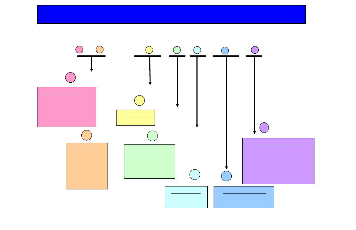
8QGHUVWDQGLQJ0RGHO1XPEHUVIRU/*'LVSOD\’V
08– 3=9
352'8&77<3(
• 00RQLWRU
• '%,'LJLWDO7XQHU
• .%,'9'
• 5%,$QDORJ7XQHU
• 7%,395
5(*,21
• 81$PHULFD
• =(XURSH
• 71(8
• 36$PHULFD
• --DSDQ
• 1.RUHD
'LVSOD\6L]H
,QFKHV
63(&,$/237,21
',63/$<'(9,&(
33'3
//&'
))ODW&57
60LFUR'LVSOD\
$VSHFW5DWLR
• =<;…ZLGH
• $%&…
(QJLQHHULQJ7RRO
)RUPDQXIDFWXULQJ
SXUSRVHRQO\
++LJK$OWLWXGH
93LYRW9HUWLFDO'LVSOD\
0+LJK$OWLWXGH3LYRW
4+RPH6HFXULW\1HWZRUN
''/3
//&'
5

Introduction to Plasma
How the power supply works
Voltages for VS: Supplies support to the Y-Amplifier for
horizontal grid voltage. If the required voltage is not + or –
3% you may see the following in the picture: lines from side
to side or left to right, half picture top or bottom, intermittent
shutdown or dead.
Voltages for VA: Supplies support to the Z-Amplifier for
vertical grid voltage. If the required voltage is not + or – 3%
you may see the following in the picture: Comets, washout,
bleeding, intermittent shutdown or dead.
To start to understand plasma one must look for why this
voltage is not within specifications. In LG – Zenith line of
plasmas there are several power supply set-ups as follows:
60” plasma is made-up of a primary and secondary power
supply followed by a DC to DC converter. This is to support
the massive current that’s required to sustain picture
quality.
The 50” and 42” plasma power supplies are consolidated
into one board. In the 60” anyone of the three parts could
be out of adjustment. In the fifty and forty two the voltages
need to be still verified in chronological order. In most
cases if your facing a dead set scenario this is caused by
a shorted Y or X-driver board.
Testing for defective Y-drive boards can be done by looking
for a voltage drop if this is located in the Y-sustain
disconnect power and remove one Y-driver boards at a
time until Y-sustain voltage is accurate. If Y-sustain does
not respond with proper voltage supplied replace. Testing
for defective X-driver boards can be done by powering
down and disconnecting each X-driver and powering on
each quadrant at a time.
Pulse Frequency Coefficient: (PFC) adjustment is Located
the primary supply and is for aligning grid voltage. The
panels grid voltage averages 360 to 380 volts depending
on panel circuit.
Known symptoms:
No Power
Intermittent Power
Picture dimming to bright during certain seines
Primary colors off, Hue or flesh tones
Colors bleeding
Left to Right picture is dark to bright
Introduction to Plasma
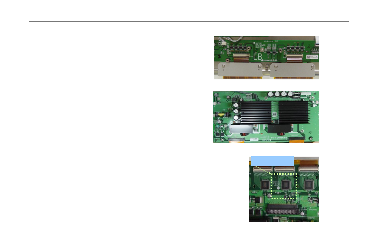
1. X B/D
Receiving LOGIC signal from CONTROL B/D to make ADDRESS
PULSE generating address discharge by an ON/OFF operation,
and supplies this waveform to COF IC (data) or ribbon IC.
X B/D
X B/D
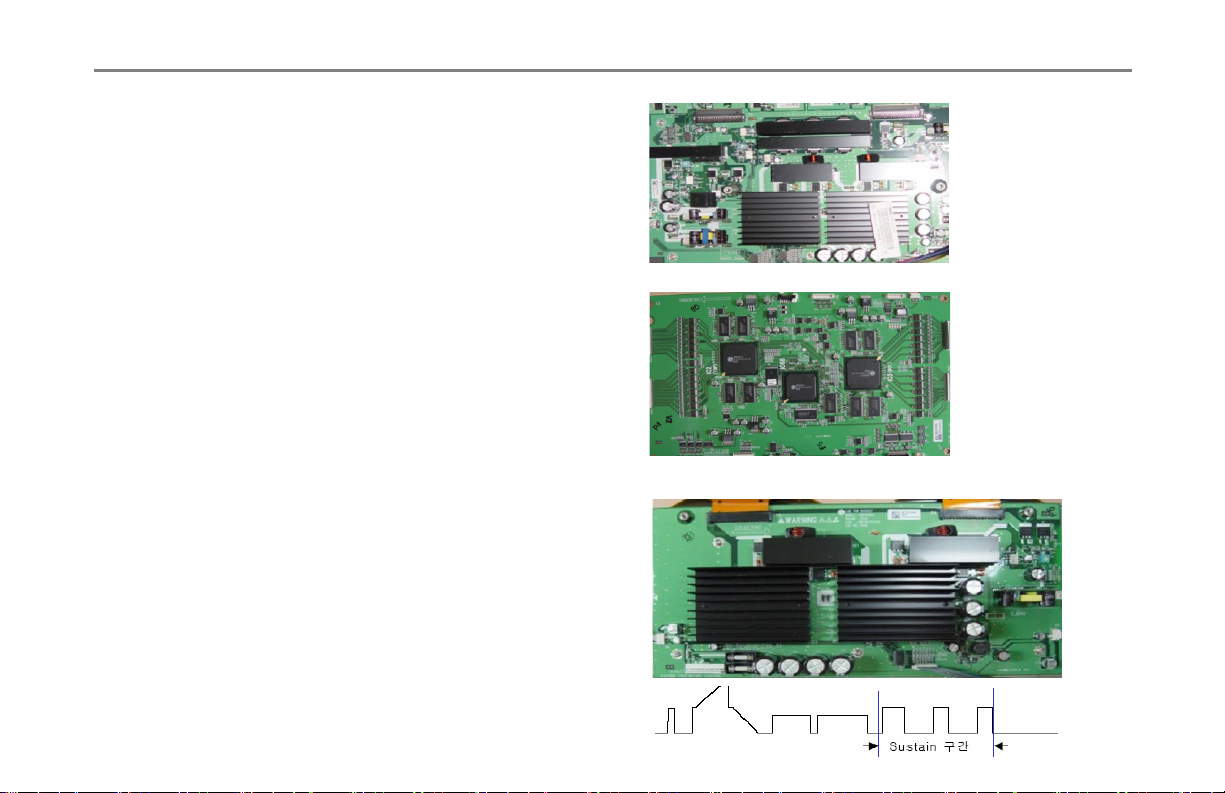
2. Z sustain B/D
Responsible for making SUSTAIN PULSE and ERASE PULSE that
that generates SUSTAIN discharge in panel by receiving LOGIC
signals the CONTROL B/D.
The Sustain discharge waveform is supplied to panel through FPC (Z
B/D).
Composed of IPM,FET,DIODE, electrolytic capacitor, E/R coil.
3. Y drive B/D
1) This is a path to supply SUSTAIN ,RESET waveform which is made
from Y SUSTAIN B/D to panel through SCAN DRIVER IC.
2) Supplies the waveform that selects Horizontal pulse (Y SUSTAIN pulse) sequentially.
- Potential difference is 0V between GND and Vpp of DRIVER IC in SUSTAIN period.
- Generated potential difference between GND and Vpp only in SCAN period.
• E/R (Energy recovery)
• COF (Chip On Film)
• IPM (Intelligent Power Module)
Z B/D
Z B/D
Y SUB--
Y SUB
AMP B/D
AMP B/D
Scan drive IC
Introduction to Plasma
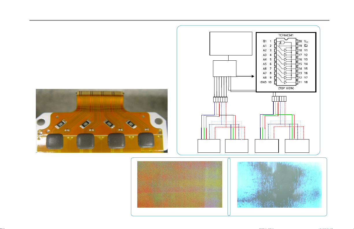
4. Y sustain B/D
Generates SUSTAIN, RESET waveform, VSC (SCAN) voltage
and supplies it to the Y DRIVER B/D.
Composed of IPM, DIODE, electrolytic capacitor, FET.
AMP B/D
YY--AMP B/D
5. Control (logic) Board
Creates signal processing (Contour noise, reduction ISM,..)
and an order of many FET switching IC’s on/ off of each
DRIVER B/D with R,G,B to each 8bit input COF ribbon IC.
Supply voltages 3.3V/ 5V.
6. IPM (Intelligent Power Module)
Connected to Z B/D and Y B/D, making Sustain waveform.
Sustaining and supplying a square wave to panel, creating video.
Composition
CAPACITORS/ DIODES/ IC LINEAR/ RESISTORS,
TRANSISTORS and FETS.
• E/R (Energy recovery)
• IPM (Intelligent Power Module)
DIG CONTROL B/D
DIG CONTROL B/D
Z-APM B/D
Introduction to Plasma
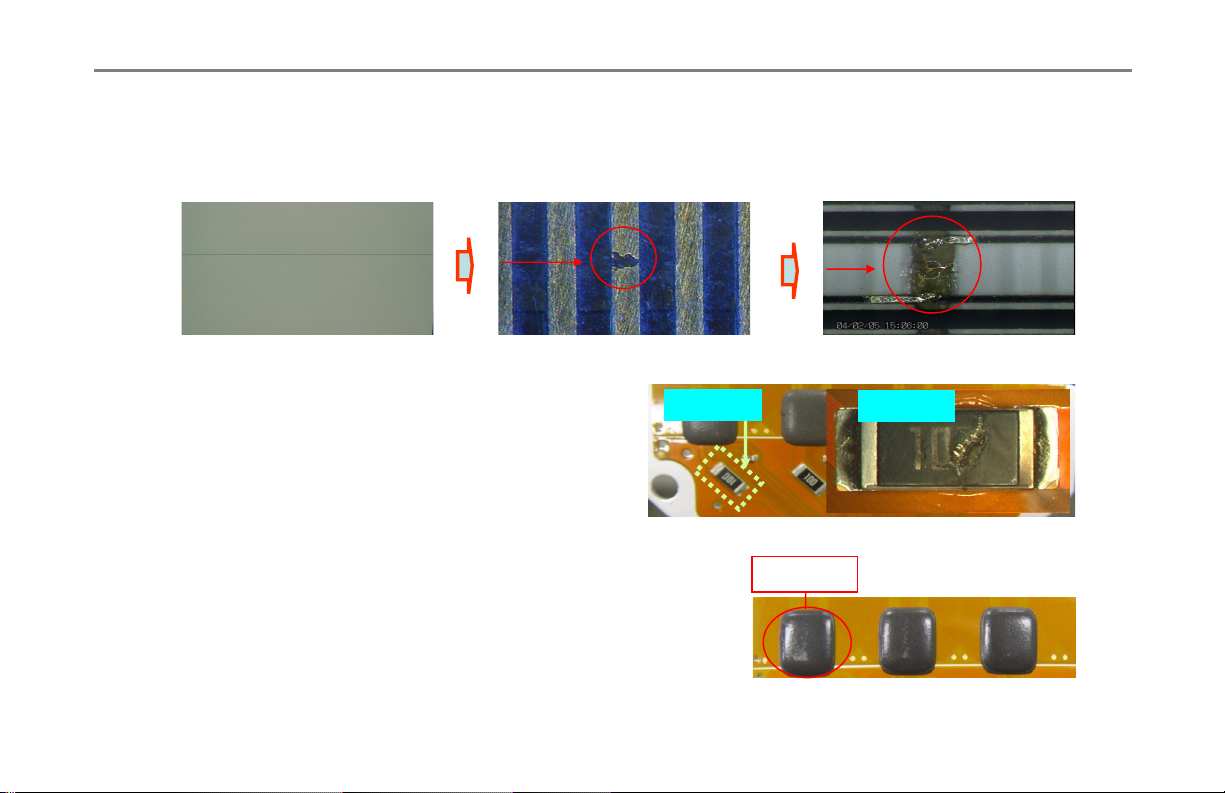
7. Ctrl B/D
CTRL B/D supplies video signal to COF. So if there is a
bar defect on panel this may be the ctrl b/d creating this
problem.
Flow, address signal
In the figure to the right shows data path to COF IC In this
description you can see how missing data can affect the
panel.
8. Checking order
1. Confirm Y, Z SUS signal cable.
2. Check Y DRV IC FAIL
3. Check Y sus b/d voltages (-Vy.Vscw)
4. Check Y ,Z-SUS IPM fail
5. Replace CTRL b/d
A. Mal-discharge problem Y-drive, Z -b/d.
<Diagram of ctrl b/d>
$6,&
Buffer
IC
$UUD\
UHVLVWRU
Each 16
lines
&2),& &2),& &2),& &2),&
B. Check VA and VS Voltage if occurred.
Introduction to Plasma
9. Check FPC
In case of horizontal 1 or more line, it is due to FPC or panel inside .ctrl b/d, Y b/d is just normal. First , clean the FPC
electrode with a cloth to clean off the ribbon connection removing particles.
Horizontal line.
COF ribbon to panel open Cell/ break down
10. Checking address COF input of resistor and IC
COF resistor check
Ⴇ
Check the both side of resistor With Digital multi meter(DMM) .
If the resistor is okay, the resistor value should be 10വif open
replace resistor.
Resistor
11. COF (Chip On Film)
Supplied with the X B/D waveform to the panel, controls grid & zones by
switching on or off the 96 pin COF IC.
the higher the resolution, the less spare space on the IC.
• E/R (Energy recovery)
• COF (Chip On Film)
• IPM (Intelligent Power Module)
Open
COF IC
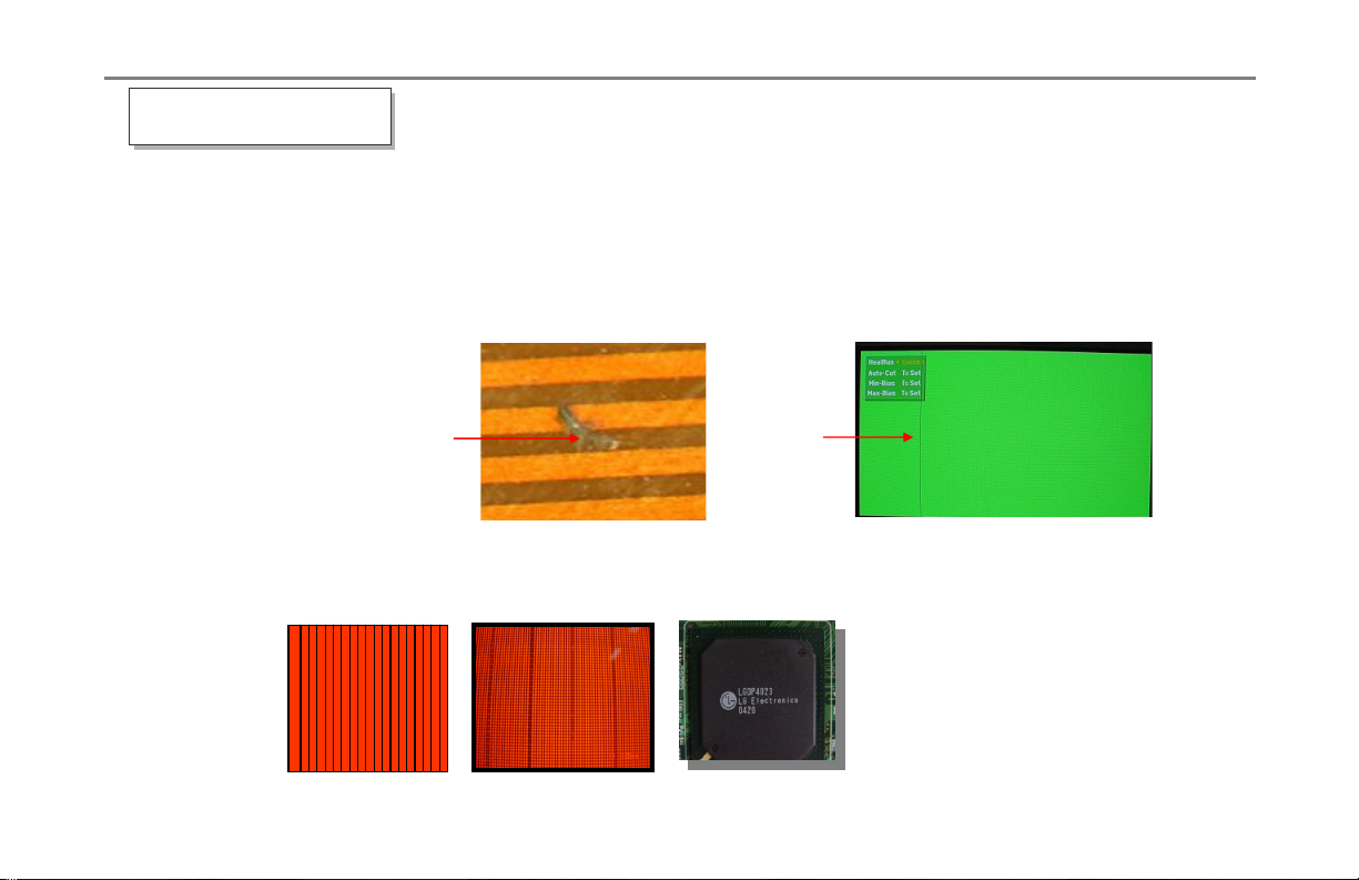
Introduction to Plasma
Vertical defect (line)
,QFDVHRIYHUWLFDOOLQHRUVKRUWFKHFNIRUIRUHLJQVXEVWDQFHVRQ&2)FRQQHFWRU
)LUVWFOHDQRIIWKHFRQQHFWRUZLWKFOHDQFORWKWRUHPRYHIRUHLJQ VXEVWDQFHV7HVWDJDLQWKHQLIWKHVDPH
OLQHDSSHDUVFKHFNIRUVKRUWHG,&6+257('UHSODFHSDQHO
1 line open or short
This phenomenon is due to COF IC inside short or adherence part of the Film and rear panel electrode
problem. In this case, replace the panel.
1 electrode open
Line open or short with same distance.
This is an ASIC of Ctrl b/d defect. ASIC defective, replace the ctrl b/d.
Will cause
1 line open
'$'DWD$UUDQJHU,&
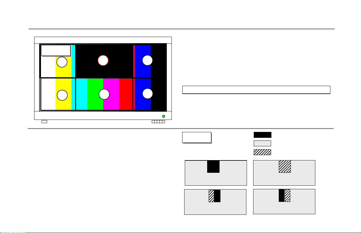
No image in the specific area (see the screen location 2)
1) Check the related X-Board’s power connector.
2) Check the signal cable between Controller PCB & X-Board.
Fig # 01
Fig # 01
1
4
2
2
5
3
6
3) Replace X-Board
Correlation between screen & X Boards
Screen Location X Board
1) Top left 3/10 l X Top-right / Bottom-left B/D
2) Center top 2/5 l X Center Top B/D
3) Top right 3/10 l X Top-left / Bottom-right B/D
4) Bottom left 3/10 l X Top-left / Bottom-right B/D
5) Center bottom 2/5 l X Center Top B/D
6) Bottom right 3/10 l X Top-right / Bottom-left B/D
Visual Troubleshooting
2. Known Tips as to no data and partial display
No image/ Data COF IC.
1) Caused by X Board’s having no power or connections.
Data COF is totally or partially not displayed
2) Check the connector between COF IC & X-Board.
3) Data COF IC is defective, replace the related X-Boards.
12
Fig # 02
Fig # 02
Examples,
Non-image
Non Image white
Partially displayed
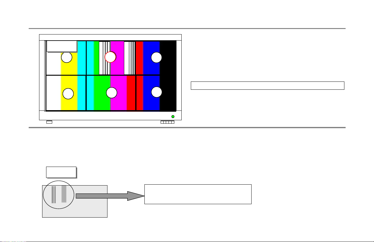
Regular vertical line with one or more Data COF IC
1) Check the related X Board’s power connector.
Fig # 03
Fig # 03
1
4
1) This is caused by X Board output IC being defective. When COF ICs have data this means the data transfer between the
Controller PCB and X Board is missing.
2) Check all related X Board connections.
3) Replace that X Board or CTRL PCB or both if needed.
Fig # 04
Fig # 04
2
5
3
6
Partial error or total error with One or more
ICs are defective.
2) Check the signal cable between Controller PCB & X-Board.
3) Replace X-Board
Correlation between screen & X Boards
Screen Location X Board
1) Top left 3/10 l X Top-right / Bottom-left B/D
2) Center top 2/5 l X Center Top B/D
3) Top right 3/10 l X Top-left / Bottom-right B/D
4) Bottom left 3/10 l X Top-left / Bottom-right B/D
5) Center bottom 2/5 l X Center Top B/D
6) Bottom right 3/10 l X Top-right / Bottom-left B/D
Visual Troubleshooting
13
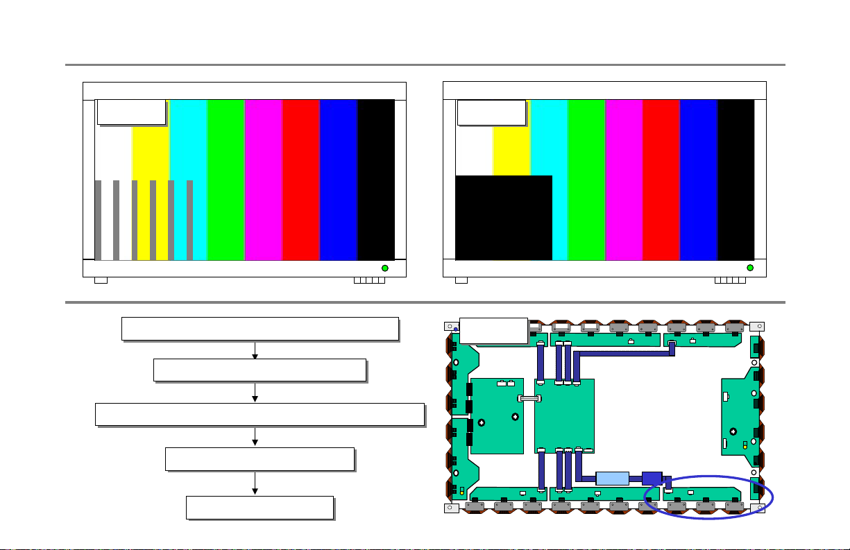
Address Bar ( Vertical ) & partial no-picture
Visual Troubleshooting
Fig # 05
Fig # 05
Related X-Board power supply voltage check
Related X-Board power supply voltage check
Related X-Board Connector check
Related X-Board Connector check
Related X-Board & Controller Board Connector check
Related X-Board & Controller Board Connector check
Related X-Board replacement
Related X-Board replacement
Module (Panel ) check
Module (Panel ) check
14
Fig # 06
Fig # 06
Bottom left 3/10 of the screen with no-pictureBottom left 3/10 of the screen with vertical bar
Fig # 07
Fig # 07
Y- Board
VR 424
B61 (TP;sus_up)
VR 301
Controller
Board
VSC
Board
P200
Side A/V L/F
Z- Board
VR 301
B61
(TP;sus_out)
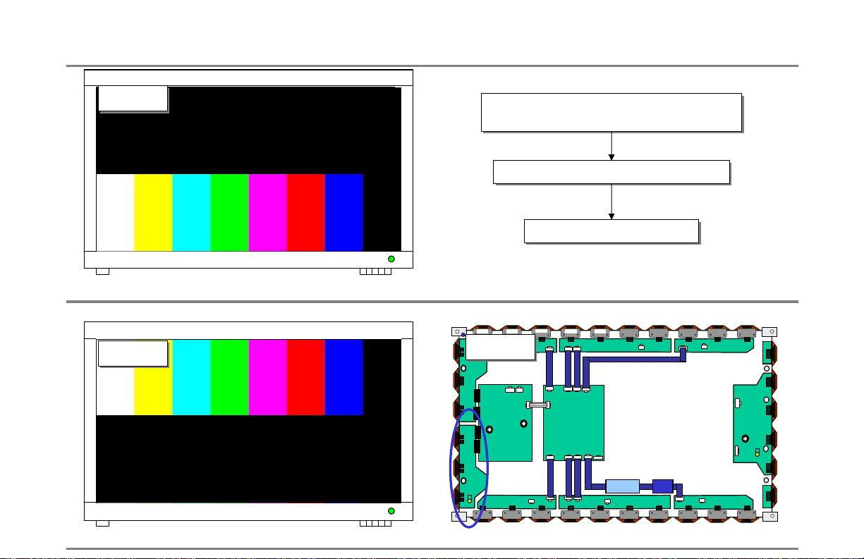
Bar (Horizontal) half -picture
Fig # 08
Fig # 08
2QO\ERWWRP,PDJHLV'LVSOD\LQJ
Fig # 09
Fig # 09
Visual Troubleshooting
<%RDUG<'ULYH%RDUG&RQQHFWRUFKHFN
<%RDUG<'ULYH%RDUG&RQQHFWRUFKHFN
Y-Drive Board ( Top ) Drive IC check
Y-Drive Board ( Top ) Drive IC check
Y-Drive Board replacement
Y-Drive Board replacement
Fig # 10
Fig # 10
Controller
Board
VSC
Board
P200
Y- Board
VR 424
VR 301
Z- Board
VR 301
B61
(TP;sus_out)
2QO\WRS,PDJHLV'LVSOD\LQJ
15
B61 (TP;sus_up)
Side A/V L/F
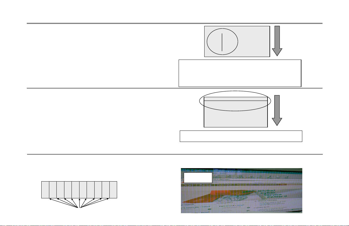
Vertical Lines
Visual Troubleshooting
6. One or more vertical lines in the screen.
1) Irregular vertical line is not related to Controller PCB or X Board.
2) It is mainly caused by the followings open (or short).
- Panel itself defect
- DATA COF FPC attached to panel is open or short.
- DATA COF attached to panel itself is defective
There can be several lines in ¼ inch wide area.
It can be seen on the both side, right and left.
The area is sometimes over ¼ inch wide.
7. One or more horizontal lines in the screen.
1) Irregular vertical line is not related to Controller PCB or Y Board.
2) It is mainly caused by the followings open (or short).
- Y FPC connector ය reinsertion
- Open because of Y Driver Board’s connector dry joint ය
Y DRV Board replacement
- Panel itself is defective, Y FPC attached to panel itself
is open or short
There can be several horizontal lines
8. Regular vertical lines in the whole screen. (mainly in one specific color, regular line is flicking)
1) This problem is related to CONTROL PCB.
2) Replace CONTROL PCB
Fig # 11
Fig # 11
Regular vertical lines in the whole screen
16
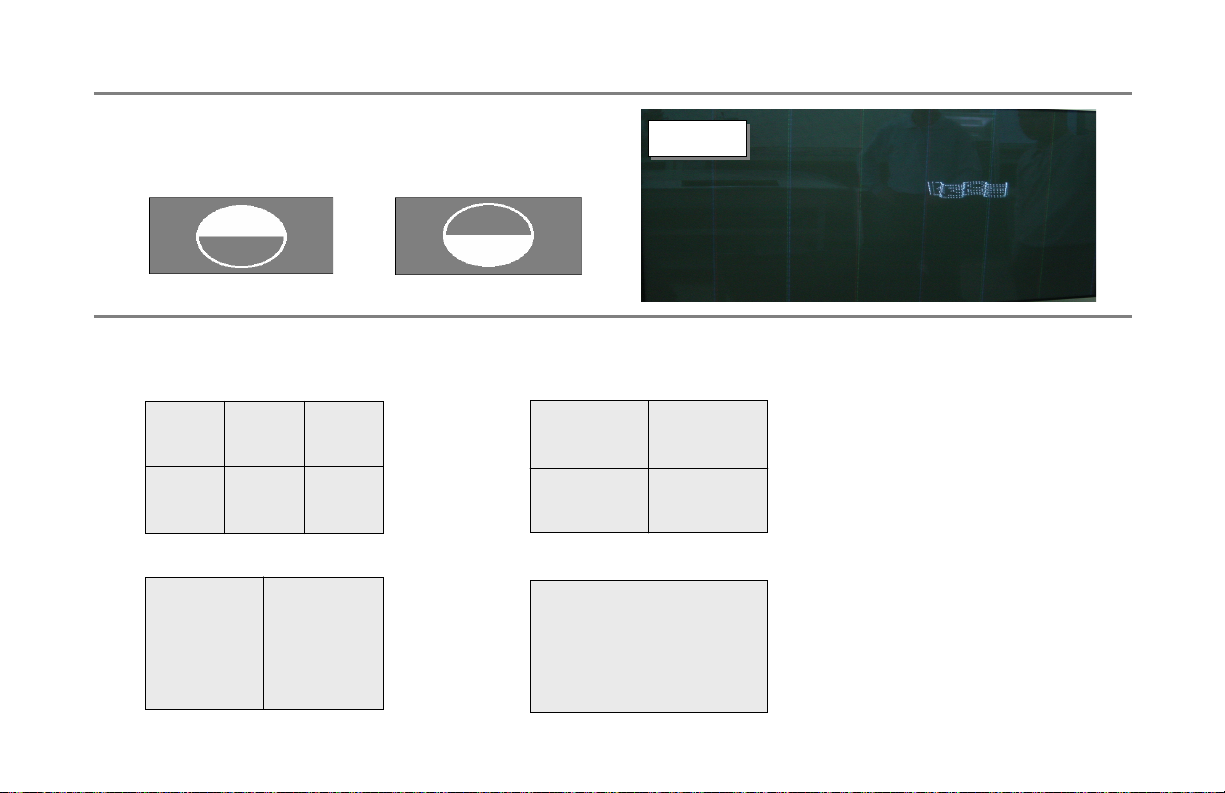
Vertical Lines
Visual Troubleshooting
9. Vertical Data copy
1) This happens when scan wave is not reproduced properly.
2) Replace Y-Board
<case 1 : partial Top copy > <case2 : partial Bottom copy >
10. Grid X and Y Layout by screen size.
60’’
X
X
Y
X
Y
50’’
40’’42’’
Fig # 46
Fig # 46
X
X
Y
Y
17
Dark picture
Visual Troubleshooting
10. Input signal pattern is displayed but the screen is dark.
1) It happens when Z Board is not operating well.
2) Check whether Z Board’s power connector is plugged properly.
3) Check whether the signal connector between Controller PCB & Z Board is plugged.
4) Replace Z Board or controller PCB.
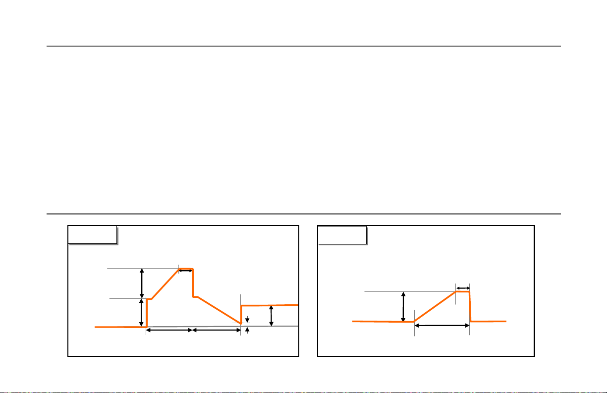
11. Input signal is white pattern but other colors are displayed in spots, missing data.
1) Check the slope & waveform of Y Board set up, set down.
2) Check the slope of Z Board’s ramp waveform
3) Measure each Board’s output waveform by over 200MHz scope and reference Fig. 12 and 13.
it is possible to control Y Board’s setup slope by adjusting VR2 and Z Board’s ramp slope by adjusting VR1.
Fig # 12
Fig # 12
Fig # 13
Fig # 13
- Y B/D measurement point : B61 ( SUS_UP OUTPUT ) - Z B/D measurement point : B61 ( SUS_OUT )
V-set-up
( 200V~240V)
Vs (170 ~ 185V)
0V
140ᓪ
< Y Sustain voltage wave>
20s5ᓪ
170s5ᓪ
VCC ( 90~110V)
10V
Vs (170 ~ 185V)
0V
3ᓪs2ᓪ
23ᓪ
< Z Ramp voltage wave >
18
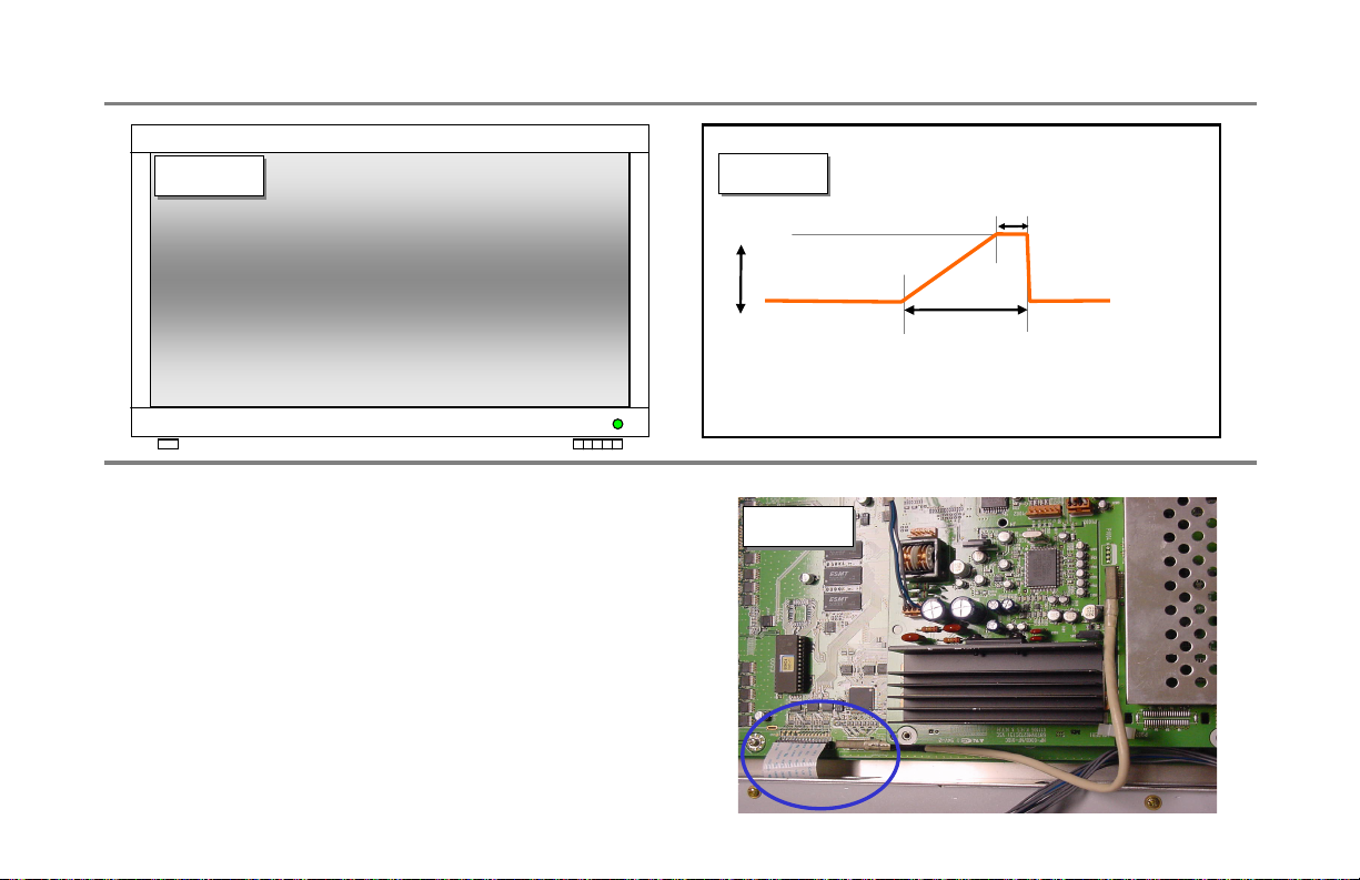
Dark picture at Top, Bottom or Center
Visual Troubleshooting
Fig # 14
Fig # 14
13. A specific brightness of one color is not clear.
1) Check CTRL Board’s input signal connector.
2) Replace CTRL Board.
14. With a full white pattern, the picture is darker toward
the center.
1) Dark picture will occur when the Z-board is missing its ramp
waveform/ see Fig # 15
2) Check the connection between CTRL PCB and the Z-board
signal cable.
3) If the signal cable is -OK- Replace the Z-Board.
Fig # 15
Fig # 15
Vs (170 ~ 185V)
Fig # 16
Fig # 16
3ᓪs2ᓪ
23ᓪ
< Z Ramp voltage wave >
19
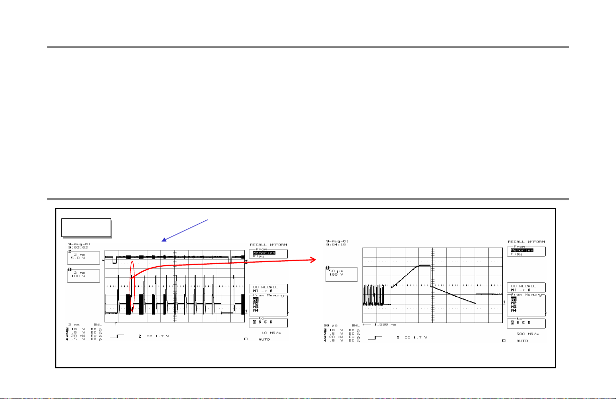
No picture
1) Check CTRL PCB’s LED (D1~ D4).
2) Check the power or signal cable inputting into CTRL PCB.
3) Check X Board, Y Board and Z Board’s power connector.
4) Check the connector between CTRL PCB, X Board, Y Board, and Z Board respectively.
5) Measure Y Board’s output waveform with over 200MHz oscilloscope and compare it to Fig 17 below.
- Y Board measurement point : ( SUS_UP OUTPUT )
- X Board measurement point : ( SUS_DN OUTPUT )
6) Test data X Board waveform @ COF IC See Fig 34 page 26.
7) No Signal - Replace Controller PCB
V_SYNC
Fig # 17
Fig # 17
amplified
Visual Troubleshooting
< Y Board output wave - 1 Frame > < Y Board output wave (amplified) - 1 SF >
20
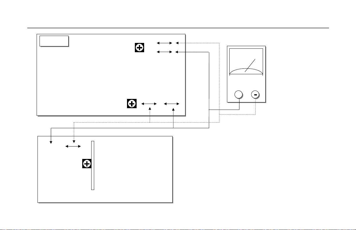
Voltage Adjustment
Fig # 18
Fig # 18
TP5 GND
Service Adjustment
When replacing power board,
Be sure to follow Power Assembly voltage Proc.
<SMPS Board>
PFC +
PFC -
VR801
VS · 1V
PFC PACK
VA Adjust
VR8401
VS Adjust
VR8501
TP3
GND
TP6 VA
TP4
VS
21
DMM
+
+
1. PFC adjustment
-. Select 100% White Pattern signal and Pre-Heat panel.
-. Connect DMM with TP PFC+ and TP PFC – (GND).
-. adjust VR801 to 380V (within ·1V ).
2. VA adjustment
-. Connect DMM + terminal with P814 #1 Pin.
-. Turn VR8401 (VA) to adjust the voltage on DMM to VA voltage
value marked on label @ bottom- right of panel. (allowable tolerance :
·0.5V )
3. VS adjustment
-. Connect DMM’s + terminal with P803 # 9 Pin.
-. Turn VR 8501 (VS)to adjust the voltage with DMM to Vs voltage
value marked on label @ bottom- right of panel.
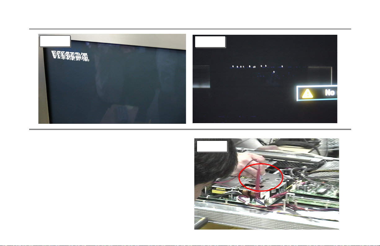
Voltage Adjustment
Service Adjustment
Fig #47
Fig #47
Problem: The picture above is an example of distorted
text.
Cure: VA & VS voltage adjustment is needed when
the following items are found:
• Distorted text
• Blocked text
• Pixilated picture
• Dots running from side to side
• Tearing in the picture
• Video smear
Fig # 48
Fig # 48
Fig # 49
Fig # 49
22
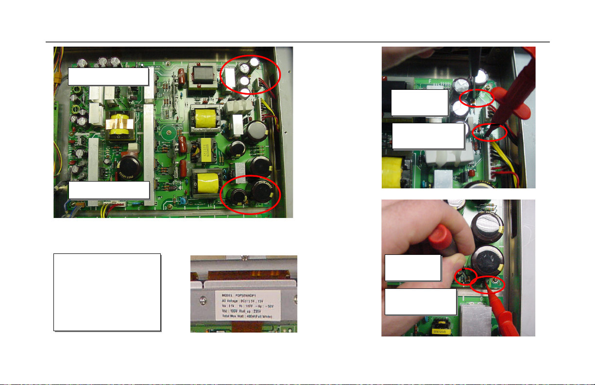
60’’ Test points and voltage adjustments.
VS adjustment
VS adjustment
VA adjustment
VA adjustment
Service Adjustment
VA adjust
VA adjust
VR8401
VR8401
VA test point
VA test point
TP-6
TP-6
The voltage settings
The voltage settings
change from model
change from model
to model and are
to model and are
labeled and located
labeled and located
at the top center of
at the top center of
the screen.
the screen.
23
VS adjust
VS adjust
VR8501
VR8501
VS test point
VS test point
TP-4
TP-4
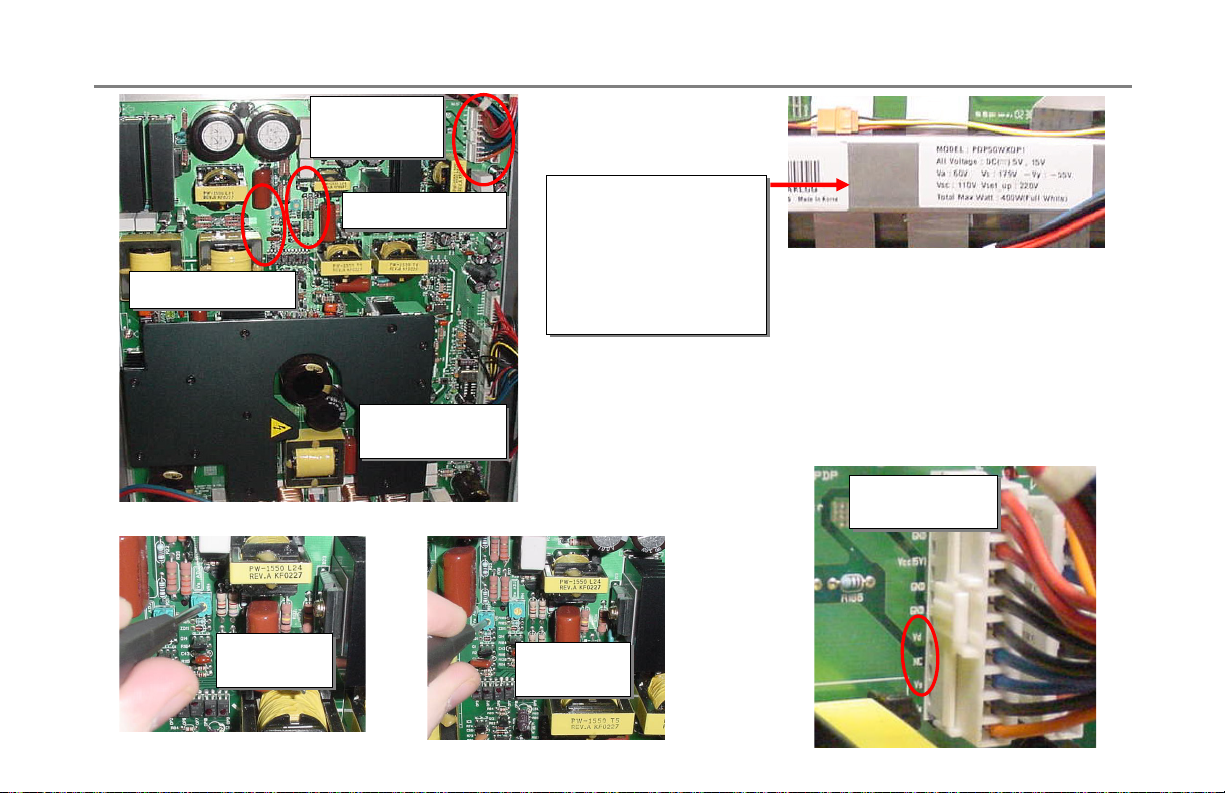
50’’- 26 series Test points and voltage adjustments.
VS/ VA
VS/ VA
Test Points
Test Points
The voltage settings
The voltage settings
change from model
change from model
to model and are
to model and are
labeled and located
labeled and located
at the top center of
at the top center of
VA adjustment
VA adjustment
VS adjustment
VS adjustment
the screen.
VS test point
VS test point
TP1
TP1
the screen.
Service Adjustment
VA test point
VA test point
VA adjust
VA adjust
RV601
RV601
VS adjust
VS adjust
RV401
RV401
24
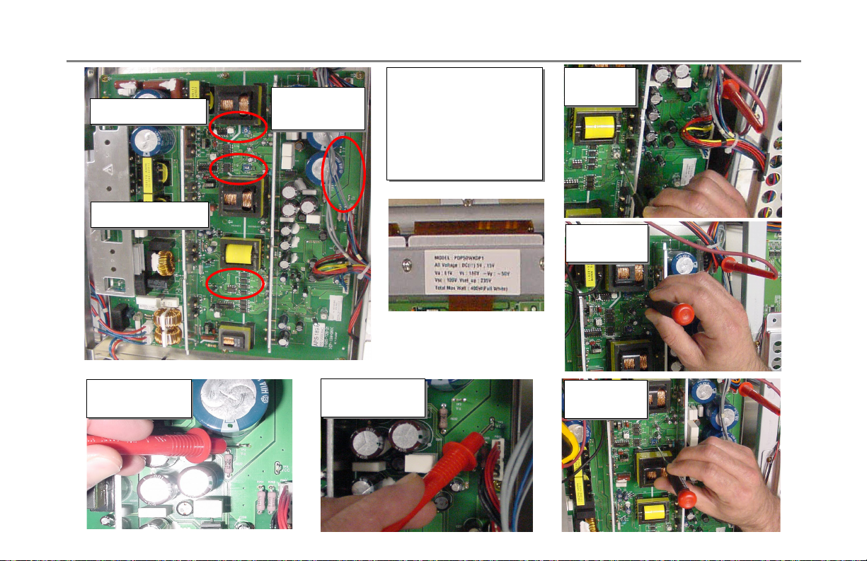
50’’- 28 Series Test points and voltage adjustments.
Service Adjustment
VS adjustment
VS adjustment
VA adjustment
VA adjustment
VA test point
VA test point
TP2
TP2
VS/ VA
VS/ VA
Test Points
Test Points
VS test point
VS test point
TP1
TP1
The voltage settings
The voltage settings
change from model
change from model
to model and are
to model and are
labeled and located
labeled and located
at the top center of
at the top center of
the screen.
the screen.
Five B +
Five B +
RV203
RV203
VS adjust
VS adjust
RV401
RV401
VA adjust
VA adjust
RV601
RV601
25
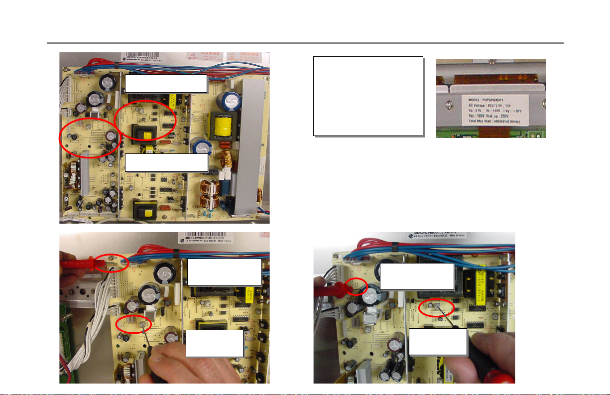
42’’ with tuner test points and voltage adjustments.
VS adjustment
VS adjustment
VA adjustment
VA adjustment
VS test point
VS test point
TP-2
TP-2
Service Adjustment
The voltage settings
The voltage settings
change from model
change from model
to model and are
to model and are
labeled and located
labeled and located
at the top center of
at the top center of
the screen.
the screen.
VA test point
VA test point
TP-1
TP-1
VS adjust
VS adjust
RV601
RV601
26
VA adjust
VA adjust
RV401
RV401
 Loading...