

Page 1
KARAOKE MINI
HOME THEATER
SERVICE MANUAL
MODEL : MDD262(MDS262V)
CAUTION
BEFORE SERVICING THE UNIT, READ THE “SAFETY PRECAUTIONS”
IN THIS MANUAL
.
MODEL : MDD262(MDS262V)
SERVICE MANUAL
P/NO : AFN32840846 FEBRUARY, 2007
http://biz.lgservice.com
Page 2

1-1
CONTENTS
SECTION 1
GENERAL
SERVICING PRECAUTIONS ......................................1-2
• NOTES REGARDING HANDLING OF THE PICK-UP
•
NOTES REGARDING COMPACT DISC PLAYER REPAIRS
ESD PRECAUTIONS ...................................................1-4
LOCATION OF USERS CONTROLS.........................1-5
SPECIFICATIONS ........................................................1-7
SECTION 2
EXPLODED VIEWS
CABINET AND MAIN FRAME SECTION..................2-1
TAPE DECK MECHANISM EXPLODED VIEW ........2-3
1. TAPE DECK MECHANISM
(A/R & A/S : RIGHT A/R DECK)........................2-3
2. TAPE DECK MECHANISM
(A/R & A/S : LEFT A/S DECK) ..........................2-5
DVD MECHANISM EXPLODED VIEW ......................2-7
SPEAKER EXPLODED VIEW ....................................2-9
MODEL : MDS262V (FRONT SPEAKERS)...........2-9
PACKING ACCESSORY VIEW.................................2-13
SECTION 3
AUDIO PART ELECTRICAL
AUDIO ELECTRICAL
TROUBLESHOOTING GUIDE....................................3-1
1. POWER (SMPS) ................................................3-1
2. P-SENS...............................................................3-2
3. VKK CHECK.......................................................3-2
4. MICOM PART CHECK I ....................................3-2
5. MICOM PART CHECK II ...................................3-3
6. IC103(KS4CD21CS) CHECK............................3-4
7. FLD DISPLAY CHECK ......................................3-5
8. PWM MODULATION PART CHECK................3-6
9. POWER AMP PART CHECK............................3-7
10. AUX FUNCTION CHECK..................................3-8
11. TUNER FUNCTION CHECK.............................3-9
12. TAPE FUNCTION CHECK ..............................3-10
13. TAPE PLAY PART CHECK..............................3-11
14. TAPE REC PART CHECK...............................3-12
INTERNAL BLOCK DIAGRAM OF ICs...................3-13
1. ES6838 ..............................................................3-13
2. HA12237F..........................................................3-14
3. PS9829B............................................................3-15
4. PT6324...............................................................3-15
5. STR-S6757IF1905 ............................................3-16
6. TAS5142.............................................................3-17
7. U1739EJ2V1UD00/KF2_E ...............................3-18
WIRING DIAGRAM ....................................................3-20
BLOCK DIAGRAM.....................................................3-22
1. SMPS BLOCK DIAGRAM...............................3-22
2. MAIN & FRONT BLOCK DIAGRAM ..............3-24
SCHEMATIC DIAGRAMS .........................................3-26
1. SMPS SCHEMATIC DIAGRAM.......................3-26
2. MAIN SCHEMATIC DIAGRAM ........................3-28
3. AMP SCHEMATIC DIAGRAM..........................3-30
4. DECK SCHEMATIC DIAGRAM .......................3-32
5. FRONT SCHEMATIC DIAGRAM.....................3-34
PRINTED CIRCUIT DIAGRAMS...............................3-36
1. MAIN P.C.BOARD ............................................3-36
2. SMPS P.C.BOARD ..........................................3-40
3. FRONT P.C.BOARD ........................................3-42
SECTION 4
DVD PART ELECTRICAL
DVD ELECTRICAL
TROUBLESHOOTING GUIDE....................................4-1
1. POWER CHECK GUIDE...................................4-1
2. TEST & DEBUG FLOW.....................................4-2
3. USB PART ..........................................................4-7
WAVEFORMS ...............................................................4-8
1. WHEN POWER ON,
RESET & DATA ETC WAVEFORM ...................4-8
2.
OPEN / CLOSE WAVEFORM AT POWER ON
.......4-9
3.
STARTING ACTION WAVEFORM IN MD DEVICE
......4-9
4. FOCUS WAVEFORM (AT CD).........................4-10
5. FOCUS WAVEFORM (AT DVD)......................4-10
6.
AT POWER ON, SPINDLE SIGNAL AT MD DECK
........4-11
7.
AT FIRST ACTION, FOCUS SIGNAL A, B, C, D
....4-11
8. TRACKING SIGNAL..........................................4-12
9. RF WAVEFORM ................................................4-12
10. DISK TYPE JUGEMENT WAVEFORM...........4-13
SCHEMATIC DIAGRAMS .........................................4-15
1. MPEG SCHEMATIC DIAGRAM .....................4-15
2. SERVO SCHEMATIC DIAGRAM ...................4-17
3. INTERFACE SCHEMATIC DIAGRAM ...........4-19
PRINTED CIRCUIT DIAGRAM .................................4-21
DVD P.C.BOARD .................................................4-21
SECTION 5
REPLACEMENT PARTS LIST
........5-1
Page 3
1-2
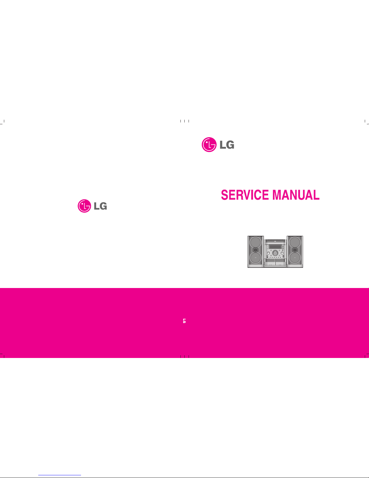
NOTES REGARDING HANDLING OF THE PICK-UP
1. Notes for transport and storage
1) The pick-up should always be left in its conductive bag until immediately prior to use.
2) The pick-up should never be subjected to external pressure or impact.
2. Repair notes
1) The pick-up incorporates a strong magnet, and so should never be brought close to magnetic materials.
2) The pick-up should always be handled correctly and carefully, taking care to avoid external pressure and
impact. If it is subjected to strong pressure or impact, the result may be an operational malfunction and/or
damage to the printed-circuit board.
3) Each and every pick-up is already individually adjusted to a high degree of precision, and for that reason
the adjustment point and installation screws should absolutely never be touched.
4) Laser beams may damage the eyes!
Absolutely never permit laser beams to enter the eyes!
Also NEVER switch ON the power to the laser output part (lens, etc.) of the pick-up if it is damaged.
5) Cleaning the lens surface
If there is dust on the lens surface, the dust should be cleaned away by using an air bush (such as used
for camera lens). The lens is held by a delicate spring. When cleaning the lens surface, therefore, a cotton
swab should be used, taking care not to distort this.
6) Never attempt to disassemble the pick-up.
Spring by excess pressure. If the lens is extremely dirty, apply isopropyl alcohol to the cotton swab. (Do not
use any other liquid cleaners, because they will damage the lens.) Take care not to use too much of this
alcohol on the swab, and do not allow the alcohol to get inside the pick-up.
SERVICING PRECAUTIONS
SECTION 1 GENERAL
Page 4
1-3
NOTES REGARDING COMPACT DISC PLAYER REPAIRS
1. Preparations
1) Compact disc players incorporate a great many ICs as well as the pick-up (laser diode). These components
are sensitive to, and easily affected by, static electricity. If such static electricity is high voltage, components
can be damaged, and for that reason components should be handled with care.
2) The pick-up is composed of many optical components and other high-precision components. Care must be
taken, therefore, to avoid repair or storage where the temperature of humidity is high, where strong
magnetism is present, or where there is excessive dust.
2. Notes for repair
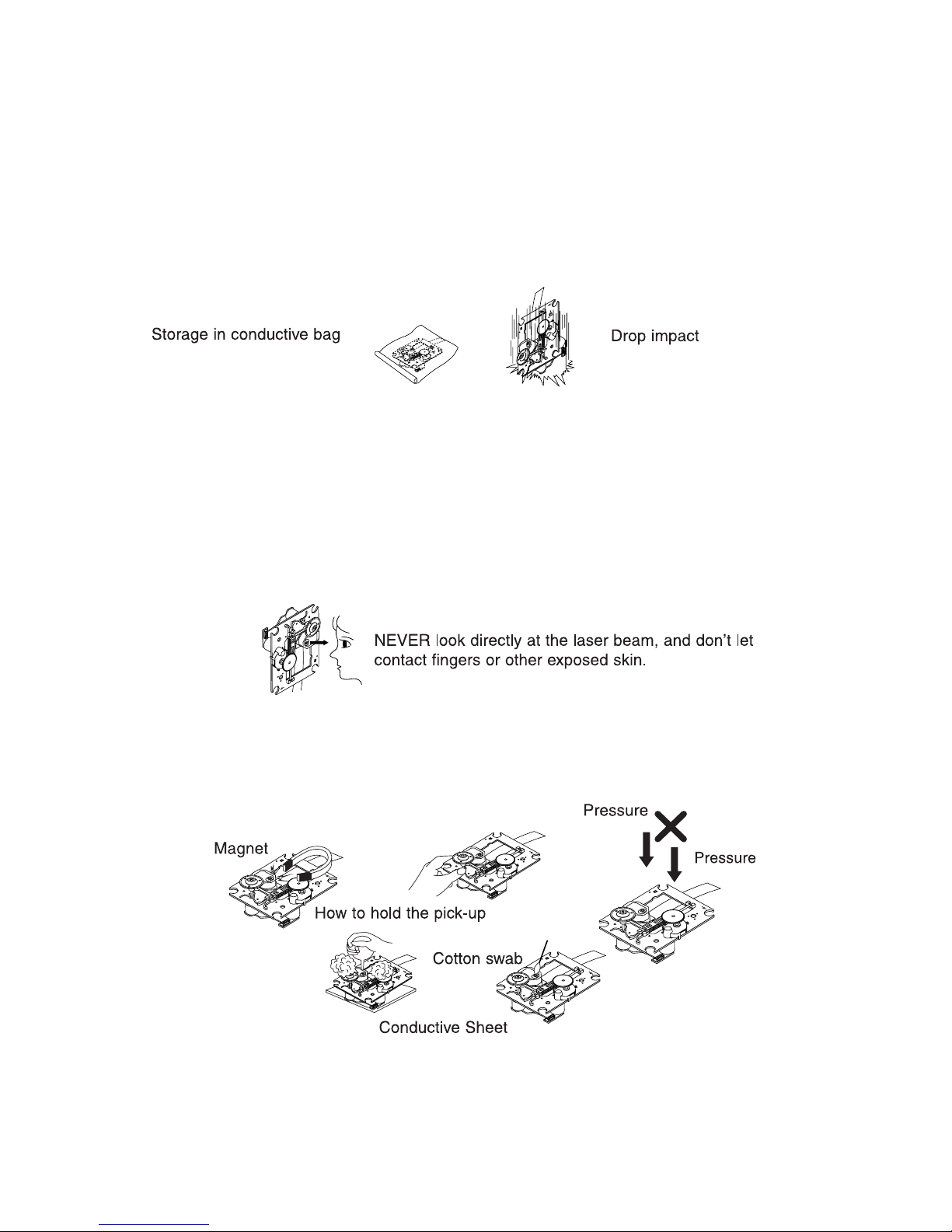
1) Before replacing a component part, first disconnect the power supply lead wire from the unit
2) All equipment, measuring instruments and tools must be grounded.
3) The workbench should be covered with a conductive sheet and grounded.
When removing the laser pick-up from its conductive bag, do not place the pick-up on the bag. (This is
because there is the possibility of damage by static electricity.)
4) To prevent AC leakage, the metal part of the soldering iron should be grounded.
5) Workers should be grounded by an armband (1MΩ)
6) Care should be taken not to permit the laser pick-up to come in contact with clothing, in order to prevent
static electricity changes in the clothing to escape from the armband.
7) The laser beam from the pick-up should NEVER be directly facing the eyes or bare skin.
CLEARING MALFUNCTION
You can reset your unit to initial status if malfunction occur(button malfunction, display, etc.).
Using a pointed good conductor(such as driver), simply short the RESET jump wire on the inside of
the volume knob for more than 3 seconds.
If you reset your unit, you must reenter all its settings(stations, clock, timer)
NOTE: 1. To operate the RESET jump wire, pull the volume rotary knob and release it.
2. If you wish to operate the RESET jump wire, it is necessary to unplug the power cord.
Page 5

1-4
ESD PRECAUTIONS
Electrostatically Sensitive Devices (ESD)
Some semiconductor (solid state) devices can be damaged easily by static electricity. Such components
commonly are called electrostatically sensitive devices (ESD). Examples of typical ESD devices are
integrated circuits and some field-effect transistors and semiconductor chip components. The following
techniques should be used to help reduce the incidence of component damage caused by static electricity.
1. Immediately before handling any semiconductor component or semiconductor-equipped assembly, drain
off any electrostatic charge on your body by touching a know earth ground. Alternatively, obtain and
wear a commercially available discharging wrist strap device, which should be removed for potential
shock reasons prior to applying power to the unit under test.
2. After removing an electrical assembly equipped with ESD devices, place the assembly on a conductive
surface such as aluminum foil, to prevent electrostatic charge buildup or exposure of the assembly.
3. Use only a grounded-tip soldering iron to solder or unsolder ESD devices.
4. Use only an anti-static solder removal device. Some solder removal devices not classified as "anti-static"
can generate electrical charges sufficient to damage ESD devices.
5. Do not use freon-propelled chemicals These can generate electrical charges sufficient to damage ESD
devices.
6. Do not remove a replacement ESD device from its protective package until immediately before you are
ready to install it. (Most replacement ESD devices are packaged with leads electrically shorted together
by conductive foam, aluminum foil or comparable conductive materials).
7. Immediately before removing the protective material from the leads of a replacement ESD device, touch
the protective material to the chassis or circuit assembly into which the device will by installed.
CAUTION : BE SURE NO POWER IS APPLIED TO THE CHASSIS OR CIRCUIT, AND OBSERVE ALL
OTHER SAFETY PRECAUTIONS.
8. Minimize bodily motions when handing unpackaged replacement ESD devices. (Otherwise harmless
motion such as the brushing together of your clothes fabric or the lifting of your foot from a carpeted floor
can generate static electricity sufficient to damage an ESD device).
[CAUTION. GRAPHIC SYMBOLS]
THE LIGHTNING FLASH WITH ARROWHEAD SYMBOL. WITHIN AN EQUILATERAL
TRIANGLE, IS INTENDED TO ALERT THE SERVICE PERSONNEL TO THE PRESENCE
OF UNINSULATED "DANGEROUS VOLTAGE" THAT MAY BE OF SUFFICIENT
MAGNITUDE TO CONSTITUTE A RISK OF ELECTRIC SHOCK.
THE EXCLAMATION POINT WITHIN AN EQUILATERAL TRIANGLE IS INTENED TO
ALERT THE SERVICE PERSONNEL TO THE PRESENCE OF IMPORTANT SAFETY
INFORMATION IN SERVICE LITERATURE.
Page 6

1-5
LOCATION OF USERS CONTROLS
FRONT / BACK PANEL
1
3
4
5
6
7
8
9
10
11
12
13
2
18
15
19
14
17
16
MDD262 Model
MDT352 Model
20
1. NUMERIC buttons (0-9)
2. DISPLAY WINDOW
3. • ( )POWER button
• CLOCK button
• TIMER button
• DUBBING (DUBB.) / CD SYNCHRO RECORDING
(CD SYNC.) / (ST./MO.) button
4. MULTI JOG
• MANUAL TUNING
• CD SKIP
• CLOCK ADJUST
• (b-KEY CON-#) KEY CONTROL
5. HEADPHONE Jack (PHONES): ø3.5 mm
6. USB ( ) connector
7. • FUNCTION SELECT buttons
(TUNER, TAPE, KARAOKE/DVD/CD, AUX)
• EQ button
• XTS-PRO button
• USB button
• XDSS Plus button
• Volume control knob
8. PUSH EJECT position (TAPE 1)
9. PUSH EJECT position (TAPE 2)
10.• RECORD/RECORD PAUSE ( REC/ ) button
• TUN.(-/+) buttons -AUTO TUNING /
REWIND / FAST FORWARD ( ) -TAPE/
SCAN ( ) /TEMPO (-/+) buttons -CD
• PRESET (-/+) buttons / TAPE REVERSE PLAY
() button (OPTIONAL) / TAPE FORWARD PLAY
() button
• STOP ( STOP) button
11. MIC JACKS (MIC1, MIC2): ø6.3 mm : OPTIONAL
12.MIC VOLUME knob
13.Remote control sensor
14.• OPEN/CLOSE ( OP/CL) button
• DISC SKIP (D.SKIP) button
• PLAY MODE, DEMO button
• SET/CD , RDS (OPTIONAL) button
15.DISC DOOR
16.• COMPONENT VIDEO OUT
(PROGRESSIVE SCAN) (Y Pb Pr) Connector
• VIDEO OUT Connector
17.• FM/AM ANTENNA Connector
• AUXILIARY INPUT (AUX IN) connector
18.POWER CORD
19.SPEAKER Connectors (MDT352 Model)
20.SPEAKER Connectors (MDD262 Model)
Page 7
1-6
1. POWER button
2. FUNCTION SELECT buttons
(TUNER/BAND, DVD/KARAOKE, AUX, USB)
3. NUMERIC buttons (0-9)
4. TAPE FUNCTION buttons
• REVERSE PLAY ( )
• PLAY ( )
• REWIND / FAST FORWARD PLAY ( )
• TAPE 1-2 SELECT buttons (1-TAPE-2)
• RECORD / RECORD PAUSE ( / )
• TAPE STOP ( )
5. SETUP button
6. • ARROW buttons ( / )
(Selects an option in the menu)
• PRESET (-/+) buttons ( )
• TUN. (-/+) buttons ( )
7. SELECT/ENTER button
8. MENU button
(Use the MENU button to display the menu screen
included on DVD video discs.)
9. STOP ( ), PAUSE( )/ STEP, PLAY ( ) buttons
10.PROG./MEMO., REPEAT, REPEAT A-B buttons
11. EQ ,XTS-Pro, SOUND / FEMALE( ),
AUDIO / MALE( ), SUBTITLE (S-TITLE),
SHADOW, CLEAR buttons
12.ECHO VOL. ( ) buttons
13.MIC VOL. ( ) buttons
14.RDS, PTY buttons - OPTIONAL
15.XDSS plus, VSM (Virtual Sound Matrix), ZOOM,
RETURN ( ) buttons
16.• MARKER, SEARCH, MUTE( ) buttons
• TEMPO (-/+)/ SCAN ( )
• KEY CON (b/#)/ SKIP ( )
17.VOLUME -/+ buttons
18.TITLE button
(Use the TITLE button to display the title screen
included on DVD video discs.)
19.DISPLAY button
20.DIMMER button
21.SLEEP button
22.DISC SKIP (D.SKIP) button
REMOTE CONTROL
PRESET
PRESET + +
PRESET
PRESET - -
SETUP
SETUP
TEMPO
TEMPO
MENU
MENU
REPEA
REPEA
T
MARKER
MARKER
SEARCH
SEARCH
REPEA
REPEA
T A-B
A-B
PROG./MEMO.
PROG./MEMO.
ZOOM
ZOOM
EQ
EQ
AUDIO
AUDIO
S-TITLE
S-TITLE
RETURN
RETURN
RDS
RDS
PTY
PTY
CLEAR
CLEAR
TITLE
TITLE
DISPLA
DISPLA
Y
SLEEP
SLEEP
DIMMER
DIMMER
AUX
AUX
DVD/
DVD/
KARAOKE
KARAOKE
POWER
POWER
/ENTER
SELECT
MUTE
MUTE
TUNER/BAND
TUNER/BAND
USB
USB
D.SKIP
D.SKIP
STSTOP
OP
PLA
PLA
Y
PAUSE/STEP
AUSE/STEP
ECHO VOL.
ECHO VOL.
MIC VOL.
MIC VOL.
TUN. -
TUN. -
TUN. +
TUN. +
1 -
1 -
TAPE - 2
APE - 2
SHADOW
SHADOW
KEY
KEY
CON - #
CON - #
b -
b -
XTS Pro
XTS Pro
XDSS plus
XDSS plus
VSM
VSM
SOUND
SOUND
1
6
5
4
3
2
8
9
21
20
18
16
17
19
7
10
12
13
15
11
22
14
Page 8

1-7
SPECIFICATIONS
• GENERAL
Power supply Refer to the main label.
Power consumption Refer to the main label.
Net Weight 8.65kg (MDT352)
5.9kg (MDD262)
External dimensions
(W x H x D)
280 X 365 X 370mm
• TUNER/AMPLIFIER
FM Tuning Range 87.5 ~ 108.0MHz or 65 ~74MHz, 87.5 ~ 108.0MHz
Intermediate Frequency 10.7MHz
Signal to Noise Ratio 60/55dB (Mono/Stereo)
Frequency Response 140 ~ 10000Hz
AM Tuning Range 522 ~ 1620kHz or 520 ~ 1720kHz
Intermediate Frequency 450kHz
Signal to Noise Ratio 30dB
Frequency Response 140 ~ 1800Hz
Output Power Front: 130W + 130W (4Ω, THD 10%)(MDD262)
100W + 100W (4Ω, THD 10%)(MDT352)
Subwoofer: 150W (3Ω, THD 10%)(MDT 352)
T.H.D 0.5%
Frequency Response 42 ~ 20000Hz
Signal-to-noise ratio 75dB
• DVD/VCD/CD PLAYER • CASSETTE TAPE PLAYER
Frequency response (audio) 40 ~ 20000Hz Tape Speed 3000 ± 3%
Signal-to-noise ratio (audio) More than 75dB (1kHz) (MTT-111.
Signal-to-noise ratio (video) More than 55dB (1kHz) NORMAL-SPEED)
Dynamic range (audio) More than 75dB Wow Flutter 0.25%
Video output 1.0V (p-p), 75Ω (MTT-111, JIS-WTD)
S-video output (Y) 1.0V (p-p), 75Ω F.F/REW. Time 120sec (C-60)
(C) 0.3V (p-p), 75Ω Frequency Response 250 ~ 8000Hz
Component Video output (Y) 1.0V (p-p), 75Ω Signal to Noise Ratio 43dB
(Pb)/(Pr) 0.7V (p-p), 75Ω Channel Separation 45dB (P/B)/45dB (R/P)
Erase Ratio 55dB (MTT-5511)
• SPEAKERS
Speaker Name Front Speaker (L/R) (MDS352V / MDS262V)
Type Bass Reflex 2Way 3Speaker
Impedance 4Ω
Frequency Response 55 ~ 20000Hz
Sound Pressure Level 82dB/W (1m)
Rated Input Power 130W
Max. Input Power 260W
Net Dimensions (W x H x D) 212 X 414 X 305mm
Net Weight 6.3kg
Speaker Name Subwoofer (MDS352W)
Type Bass Reflex 1Way 1Speaker
Impedance 3Ω
Frequency Response 50 ~ 1500Hz
Sound Pressure Level 82dB/W (1m)
Rated Input Power 180W
Max. Input Power 360W
Net Dimensions (W x H x D) 212 X 414 X 305mm
Net Weight 6.3kg
Page 9

1-8
MEMO
Page 10
255
256
450
450
263
262
273
455
450
H
K
A
B
E
N
N
C
F
G
J
I
A26
A40
A47
A46
266
305
267
289
456
450
264
452
458
450
450
290
290
454
450
450
A00
257
255
259
A43
A44
253
453
253
254
252
450
450
450
CABLE4
CABLE3
CABLE1
CABLE5
CN201
P9701
P9702
260
MAIN
SMPS
291
B
M
A
L
C
O
O
D
K
H
L
J
D
I
M
A41
450
CABLE2
P5701
DVD
FRONT
252
450
282
258
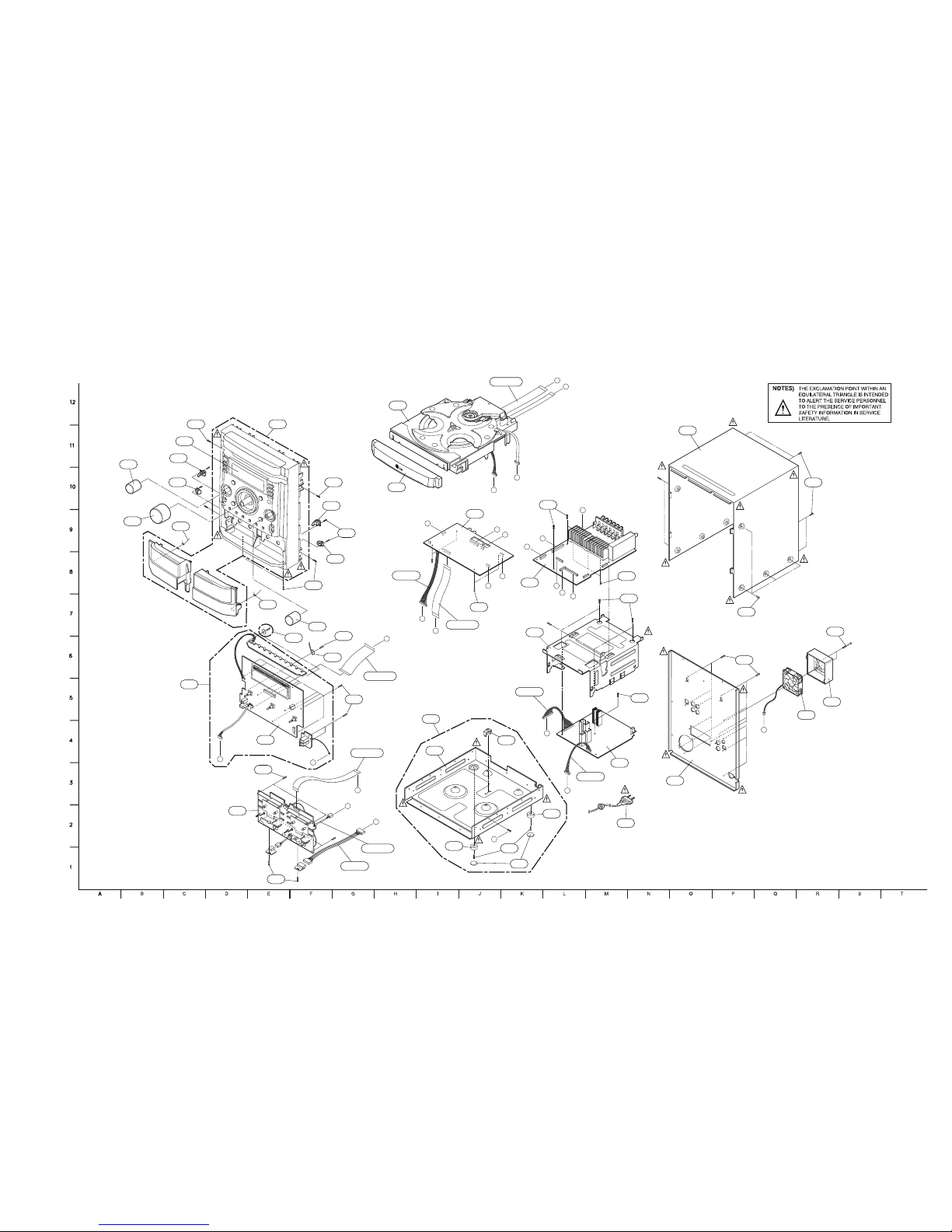
2-1 2-2
SECTION 2 EXPLODED VIEWS
CABINET AND MAIN FRAME SECTION
Page 11
001
A00
002
037
007
006
008
016
017
018
019
020
003
009
009
A02
A01
011
013
022
025
015
023
BRASS MOTOR PULLEY MAYBE CHANGED
FOR WOW FLUTTER WHEN NECESSARY
RING FW MAYBE ADDED
FOR WOW FLUTTER WHEN NECESSARY
RING FW MAYBE ADDED
FOR WOW FLUTTER WHEN NECESSARY
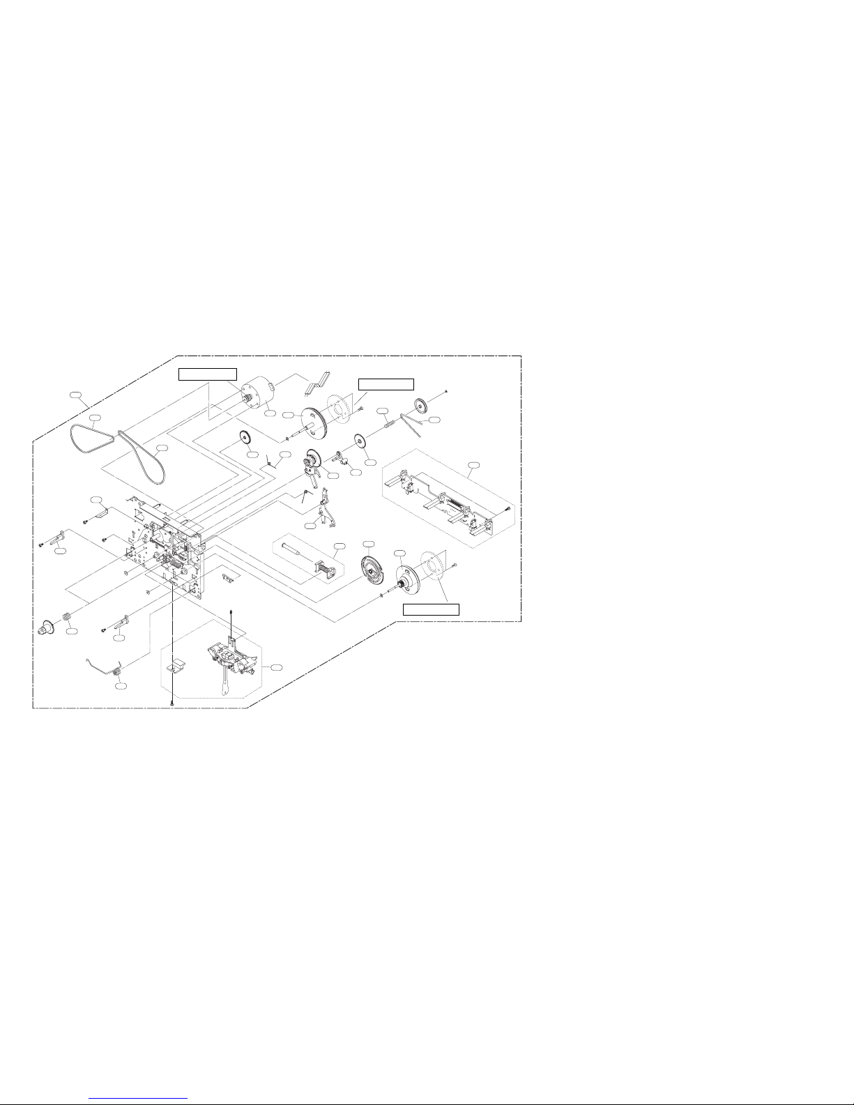
2-3 2-4
TAPE DECK MECHANISM EXPLODED VIEW
1. TAPE DECK MECHANISM (A/R & A/S : RIGHT A/R DECK)
Page 12

2-5 2-6
A00
RING FW MAYBE ADDED
FOR WOW FLUTTER WHEN NECESSARY
013
011
009
009
003
008
015
022
023
024
016
017
018
019
020
007
A03
2. TAPE DECK MECHANISM (A/R & A/S : LEFT A/S DECK)
Page 13
2-7 2-8
416
151
159
165
164
417
166
417
167
416
177
175
172
180
417
170
419
417
418
418
169
A30
A26
181
432
431
435
430
430
438
035
021
035A
036
430
012A
012A
012A
439
025
024
030
156
155
153
173
169A
169B
169C
168
163
162
441
440
422
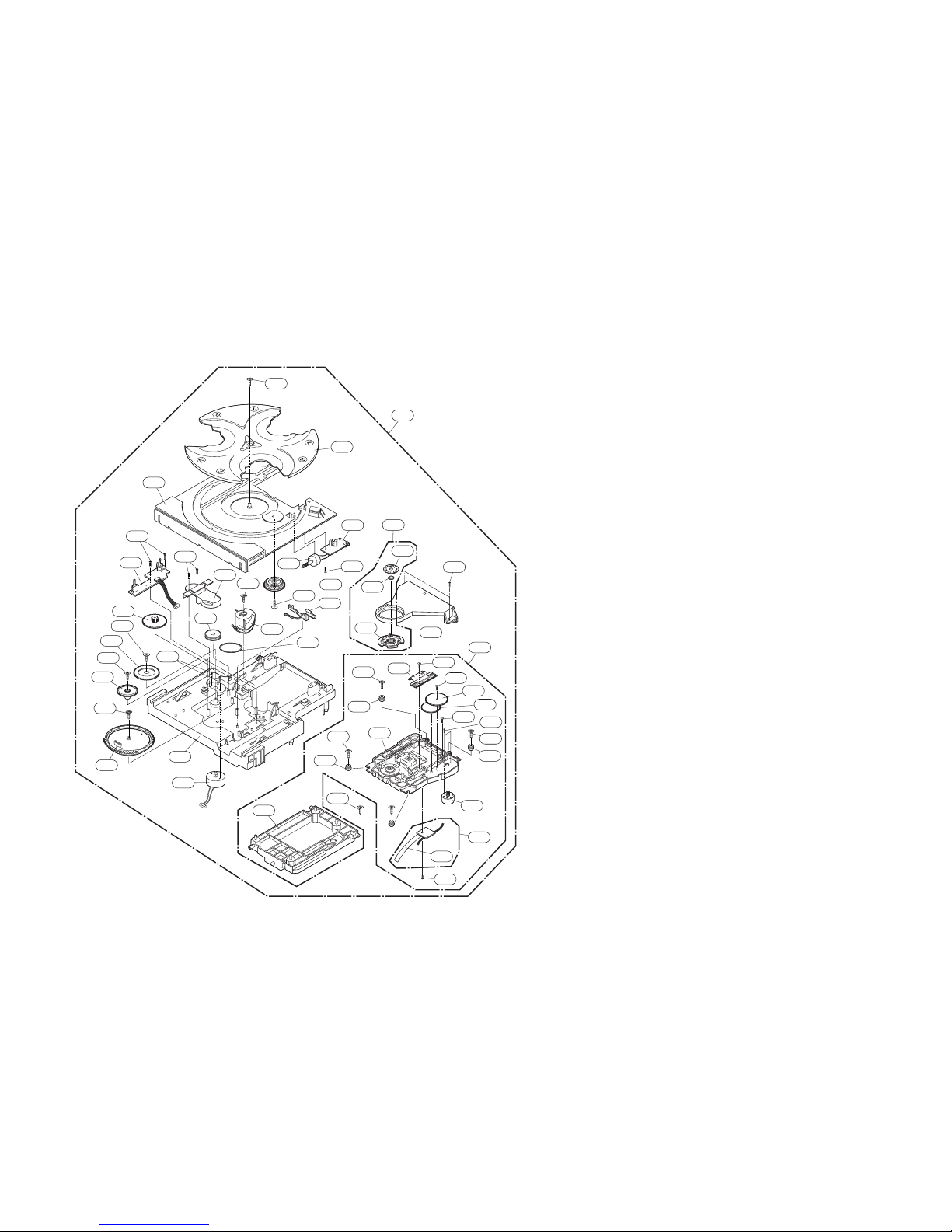
DVD MECHANISM EXPLODED VIEW
Page 14
A80A
A80R
A80L
A80BR
A80BL
WIRE80
WIRE81
850
855
856
857
858
860
861
863
859
851
853
852
854
862
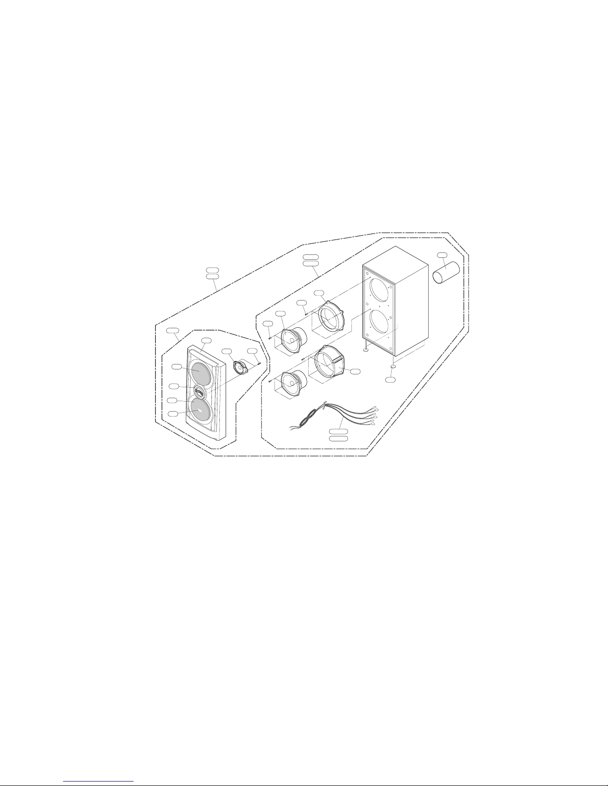
2-9 2-10
SPEAKER EXPLODED VIEW
MODEL : MDS262V (FRONT SPEAKERS)
Page 15

2-11 2-12
MEMO MEMO
Page 16
2-13
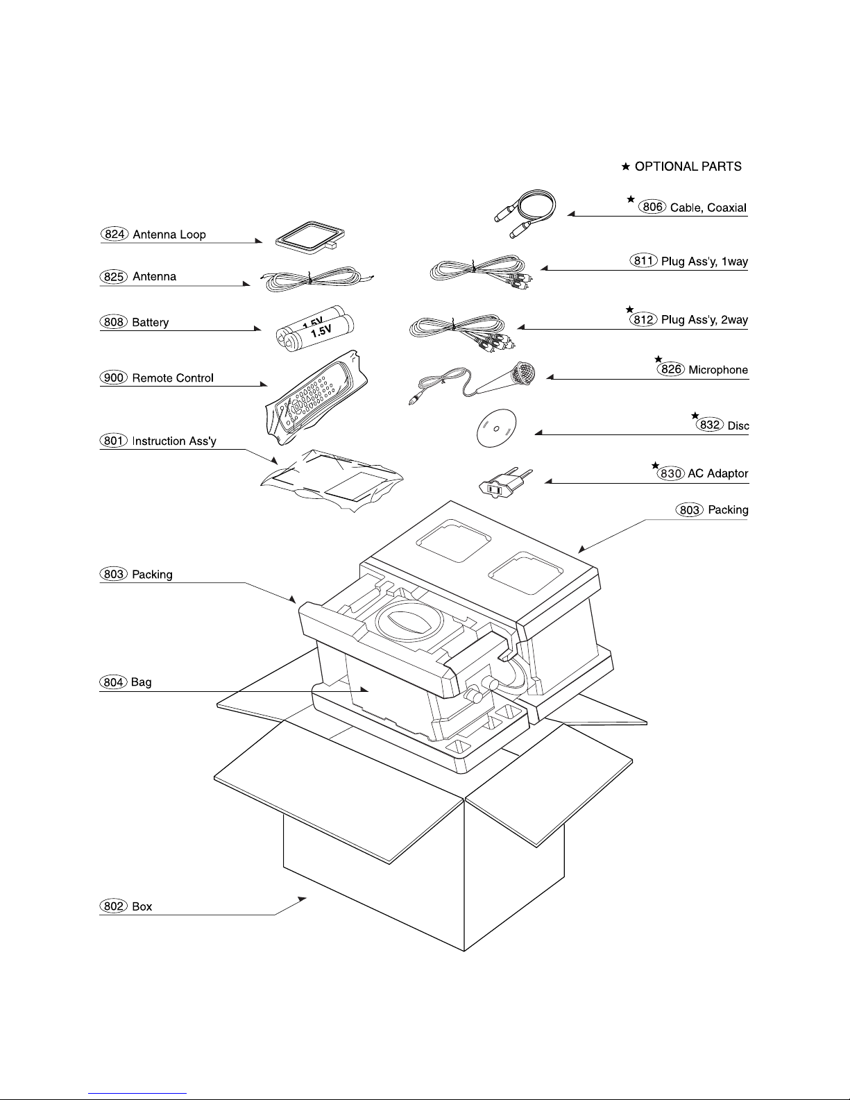
PACKING ACCESSORY VIEW
Page 17
3-1
AUDIO ELECTRICAL TROUBLESHOOTING GUIDE
SECTION 3 AUDIO PART ELECTRICAL
1. POWER (SMPS)
POWER (SMPS)
OK
YES
YES
YES
Replace IC 901,902
Check IC901, 902
Check the fuse
F901
NONO
NO
YES
Check short of
P9701, P9702 line
Replace the fuse
Check
the DC V of C905.
If DC V is over
400V
NO
Check BD901, LF901, 902
Check the
DC V of C981, C945.
If DC V is 6.1V
NO
Check short of P9702 line
YES
YES
Chcek the
DC V of C950, C951
If DC V is in
35.5V
NO
Check short of P9701 line
Chcek the
DC V of C909, C903,
C921 If DC V is in 14~19V
and it is steady.
YES
Page 18

3-2
2. P-SENS
P-SENS
YES
YES
Check
the PIN6 of P9702
If DC V is over 5.6V
Check power circuit Trouble shooting
NO
OK
3. VKK CHECK
VKK check
YES
YES
Check
the PIN3 of P9702
If DC V is over -28V ±2
Check power circuit Trouble shooting
NO
OK
4. MICOM PART CHECK I
MICOM part check I
OK OK
YES
YES
Check P-SENS
(P7904)_PIN6.
NO
Refer to
SMPS troubleshooting.
YES
YES
YES
Check both
end voltage of IC101
(KIA7042).
Check
if input voltage of
IC101(KIA7042) is
over 5V.
YES
NO
Check the
periphery of IC101
(KIA7042).
NO
YES
Check if IC101(KIA7042) of
output voltage is over 4.3V.
Check voltage of IC100
78KO/KF2_PIN1.
NO
Replace IC101
(KIA7042).
Page 19

3-3
5. MICOM PART CHECK II
MICOM part check II
X101 : 32.768kHz
X100 : 9.8304MHz
Check the operation.
Check
Q101_ emitter/collector
5V.
Check Q102_base
0.6V HIGH.
Check if IC103_PIN8 and
IC100_PIN19, 20, 59 are 5V.
NO NO
YES
YES
Check if
voltage of P7904_PIN5
is 5.6V.
NO
Refer to
SMPS troubleshooting.
YES
YES
YES
OK
YES
Check
both end voltage of
D101
YES
YES
Check D101.
NO
Check if output of
D101(1SR35) is 5V.
YES
YES
YES
YES
Check IC101.
Q102_collector 0.6V LOW.
OK
Check if output of IC101
(KIA7042) is over 4.3V.
OK
NO
Replace IC101.
NO
Replace D101.
YES
Check Q102.
OK
NO
Replace Q102.
Page 20

3-4
Check
IC100(78KOKF2)_
PIN 22, 24
OK
YES
YES
Refer to
micom troubleshooting
Check micom
voltage 5V.
PIN22
DATA PIN24 CLK
NONO
YES
Replace micom.
Check micom.
NO
YES
OK
6. IC103(KS4CD21CS) CHECK
Page 21

3-5
FLD display check
YES
YES
Replace P3702.
Check each
PIN voltage.
NO
NO
YES
YES
OK
Replace IC301.
Check IC301.
NO
YES
Replace IC100FLD light on?
Check IC100.
NO
YES
YES
OK
Refer to SMPS
7. FLD DISPLAY CHECK
YES
YES
Check
P7904_PIN1, 2, 3 voltage
input.
NO
Check P3702 connection.
NO
If voltage is not 5V,
check input and output
of D319(1SR35).
YES
Check P3702
connection and power.
Pin1 : FL-22 Pin2 : FL+26
Pin3 : VKK- over
26V.
YES
YES
YES
YES
OKOK
76 PIN - > DO - - >
Check DATA in Check IC100.
NO
IC100
75 PIN - > STB
77 PIN - > 4PIN DI
78 PIN - > 1PIN CLK
Check data output.
IC100 - >
Check IC301
DATA communication.
PIN PIN
75PIN - > 3PIN STB
76PIN - > 2PIN D
78PIN - > 1PIN
CLK
Check
IC301(PT6324) voltage.
Pin50 VKK : -26V
PIN9.52 : +5V
Check if both end votage
of F1, F2 are over 3.7V.
VKK : over 26V.
Page 22

3-6
8. PWM MODULATION PART CHECK
PWM modulation
part check
YES
YES
YES
YES
P7905_PIN9
3.3V checking
Check IC604(PS9829)
VDD PIN voltage(3, 7, 8,
10, 22, 29, 39, 47, 56, 65,
72, 94).
Check X601_PIN2 3.3V.
NO
Refer to
SMPS troubleshooting.
YES
YES
YES
YES
Check IC605_
PIN3 input and PIN2
output.
Check
X601 12.288MHz
operation.
Check IC605_
PIN8 3.3V.
Check IC605_
PIN3 input
Check X601
2.288MHz
NO
NO
IC604
(PS9829) PIN86 CLK
input check
NO
Check FB614
BEAD input, output and
voltage.
NO
Check X601
12.288MHz.
Replace X601.
OK
NO
OK
YES
YES
NO
Replace FB614
NO
Check IC605_
PIN2 output
YES
OK
YES
OK
Replace IC605.
NO
Check R680
(470Ω) output.
Replace R680.
NO
Check
IC604(PS9829) DATA
input.
Check each LINE
registor output.
NO
Check IC604
(PS9829) DATA input.
78 PIN->DATA
79 PIN->CLK
Check PWM
modulator output.
FL:75(+)74(-)
FR:71(+)70(-)
NO
NO
Check
DVD ASS`Y(PS9829)
communication
(P7403).
Refer to
CD troubleshooting.
NO
Check
IC100(78KOKF2)
21->PWM_CLK
22->PWM_DATA
43->PWM_REST
output.
NO
YES
YES
OK
YES
OK
Check IC604(PS9829).OK
Check
LINE registor output.
DATA:R671, CLK:R670
RST:R665
Replace R670, R671
and R665
NO
NO
Replace X601.
OK
YES
YES
YES
YES
Page 23

3-7
Power AMP part check
YES
Check each LINE registor output voltage.
IC700 : R701, 702, 726, 727
NO
Check each
IC700, 701, 702, 703
PIN1,17, 18, 19, 36 +12V
input.
Refer to SMPS troubleshooting.
YES
YES
YES
NO
P7905_3PIN : +12V,
PIN13, 14, 15 : 35V.
YES
Replace the coils
YES
NO
Check output line coil.
Check PWM modulator input.
Each IC PIN4, 6, 14, 16
YES
Power IC700, 701, 702, 703
PIN20, 27, 29, 34 output.
Check each IC700, 701, 702, 703
PIN21, 26, 29, 34 input voltage.
OK
9. POWER AMP PART CHECK
Page 24

3-8
10. AUX FUNCTION CHECK
AUX function check
Check µ-COM(IC301)_
PIN83, 84 commucation.
NO
NO
YES
Replace IC200
YES
YES
YES
Check
IC200(BU4052)_
PIN4, 11 input
waveform.
Check
IC200(BU4052)_PIN16
VDD, PIN8 VSS
power.
Refer to
SMPS troubleshooting.
NO
NO
YES
Replace IC801OK
YES
YES
Check
IC801(MC4580)_PIN 2, 6
input waveform.
Check
IC801(MC4580)_PIN4
VSS, PIN8 VDD
power.
Check IC200(BU4052)_
PIN3, 13 output waveform.
Check JK800 connection.
Page 25

3-9
11. TUNER FUNCTION CHECK
TUNER function check
YES
Check IC200(BU4052)_
PIN16 VDD, PIN8 VSS power.
NO
Check
IC200(BU4052)_PIN3, 13
output waveform and IC601
(BU4052)_PIN2,15 input
waveform.
Check TUNER module voltage(PIN2 : 9V).
YES
YES
YES
YES
NO
Check TUNER
module(TU601) operation.
YES
Check IC801(MC4580)_
PIN4 VSS, PIN8 VDD power.
YES
NO
Check IC801(MC4580)_
PIN2, 6 input waveform.
Replace IC200.
Replace IC200.
Replace IC801.
Check IC200(BU4052)_PIN1, 12 input
waveform.
OK
Page 26

3-10
12. TAPE FUNCTION CHECK
TAPE function check
YES
Check IC200(BU4052)_
PIN16 VDD, PIN8 VSS power
YES
YES
YES
NO
Check
IC200(BU4052)_PIN2, 15 input
waveform.
Check IC200(BU4052)_
PIN16 VDD, PIN8 VSS power
YES
NO
Check IC801(MC4580)_
PIN2, 6 input waveform.
YES
Replace IC200.
Replace IC200.
Replace IC200.
Check IC200(BU4052)_PIN3, 13
output waveform and IC601(BU4052)_
PIN2, 15 input waveform.
YES
TAPE PCB ASS`Y
OK
Page 27

3-11
13. TAPE PLAY PART CHECK
TAPE PALY part check
Replace head wire and tape
deck mechanism.
NO
NO
YES
YES
Check A deck head input
IC201_PIN32, 39 and B deck
head input IC201_PIN34, 37.
YES
YES
YES
YES
Check IC201_
PIN5, 26 signal
output.
Check
IC201(HA12237)_PIN16
12V input.
Check A/B
deck head input.
NO
Refer to
SMPS troubleshooting.
Check IC202_PIN10 "HIGH"
NO
Check IC201_PIN14
mute operation.
Replace IC201.
NO
YES
OK
Check IC201
YES
Replace IC202.
NO
YES
OKOK
Check IC202.
Page 28

3-12
14. TAPE REC PART CHECK
TAPE REC part check
Check IC100_PIN23 "HIGH"
NO
NO
YES
YES
Check IC201_
PIN7, 24 record input.
Check P2203_PIN5, 3 input
and PIN8 erase input.
YES
YES
YES
YES
YES
Check L203_PIN2, 3
oscillation.
Check
IC604(PS9829)_PIN49, 52
PWM output.
Check Q205(D1304)_
base "HIGH".
Replace IC201.
NO
NO
Check IC201_
PIN10, 21 output.
Check IC100_PIN23
"HIGH"
NO
Refer to PWM
modulation troubleshooting.
OK
YES
Replace IC202.
YES
OK
OK
Page 29

3-13
INTERNAL BLOCK DIAGRAM OF ICs
1. ES6838
SDRAM/ROM
Interface
GPIO
+
Gateway
DMA
Controller
Huffman
Decoder
ROM
DRAM
Interface
RAM
Video
Processor
TV-Encoder
VDAC
HDMI I/F
Display
OSD / SPU
Controller
Scaler
DeIntelacer
16 K Cache
32-Bit
RISC
Processor
Audio ADC
Serial Audio
Interface
Audio DAC
USB
DVD
Descrambler
+
Transport
ATAPI
Servo Controller / RF
8051
µController
DSC
ECC
Digital
PLL
Page 30

3-14
2. HA12237F
Page 31

3-15
3. PS9829B
MBCK
SBCK
SLRCK
MLRCK
MSDIN[0:3]
SSDIN[0:3]
MIC_MCLK
DMIX_MCLK
OLRCK
OBCK
DMIX_SDOUT
PWM1_P/M
PWM2_P/M
PWM3_P/M
PWM4_P/M
PWM5_P/M
PWM6_P/M
PWM7_P/M
PWM8_P/M
PWM_HP_L_P/M
PWM_HP_R_P/M
PWM_SWL_P/M
EPD_ENA
OVERLOAD
MIC_BCK
MIC_LRCK
MIC_SDIN
SPI/I2C
SO/SDA
SCK/SCL
SI/I2C_AD0
/
CS/I2C_AD2
EXT_MUTE
CLK_IN
/RESET
PLL_DVDD
PLL_DVSS
PLL_AVDD
PLL_AVSS
DVDD
DVSS
IO_VSS
IO_VDD
Internal Controls
Internal Clock Internal Reset
Host
Interface
(I
2
C, SPI)
Mic,
Input
Processor
Input
Mapper
Sample
Rate
Converter
Input
&
Output
MUX
Serial Audio
Output
Interface
Down
Mixer
Mixer
4 Band
EQ
Bass
Manager
Main
Volume
Trim
Volume
Serial
Audio
Output
Interface
PWM
Modulator
POP
NR
Power Supply
Output Mapper
PLL
Reset & Power Down
Automatic
Gain
Limiter
4. PT6324
SG1/KS1
SG2/KS2
SG3/KS3
SG4/KS4
SG5/KS5
SG6/KS6
SG7/KS7
SG7/KS7
SG8/KS8
SG9/KS9
SG10/KS10
SG11/KS11
SG12/KS12
SG13/KS13
SG14/KS14
SG15KS15
SG16/KS16
SG17
SG18
SG19
SG20
SG21
SG22
SG23
SG24
GR1
GR2
GR3
GR4
GR5
GR6
GR7
GR8
GR9
GR10
GR11
GR12
GR13
GR14
GR15
GR16
Segment Driver
Dimming Circuit
Grid
Driver
Control
DIN/DOUT
CLK
STB
OSC
LED1
K1 K2 VDD GND VEE
Timing Generator
Key Matrix Memory
LED
Driver
CSC
Serial
Data
Interface
Display Memory
Page 32

3-16
5. STR-S6757IF1905
4
Vcc
Start
Stop
Burst
OSC
Protection
latch
DRIVE
Reg
Delay
Burst
Control
BSD
OCP
GND
S
D
FB
FB
OCP/BD
SS/OLP
BD
Q
Q
S
S
R
R
MaxON
RQ
S
OLP
Reg&
Iconst
Soft Start
Counter
Bottom Selector
5
7
6
3
2
1
OVP
Page 33

3-17
6. TAS5142
2nd-Order L-C
Output Filter
for Each
Half-Bridge
Bootstrap
Capacitors
2-Channel
H-Bridge
BTL Mode
System
Microcontroller
OUT_A
OUT_B
OUT_C
OUT_D
BST_A
BST_B
BST_C
BST_D
RESET_AB
RESET_CD
System
Power
Supply
Hardwire
Mode
Control
PVDD
GVDD (12 V)/VDD (12 V)
GND
Hardwire
OC Limit
M1
M3
PVDD
Power
Supply
Decoupling
32 V
12 V
GND
VAC
PWM_A
PWM_C
PWM_D
PWM_B
V
ALID
M2
Left-
Channel
Output
Right-
Channel
Output
Input
HúBridge 1
Input
H-Bridge 2
GVDD
VDD
VREG
Power Supply
Decoupling
4
PVDD_A, B, C, D
GND_A, B, C, D
GVDD_A, B, C, D
4 4
VDD
GND
VREG
AGND
OC_ADJ
Bootstrap
Capacitors
2nd-Order L-C
Output Filter
for Each
Half-Bridge
SD
OTW
Output
H-Bridge 2
Output
H-Bridge 1
OTW
SD
T
AS5508
Page 34

3-18
7. U1739EJ2V1UD00/KF2_E
Port 0 P00 to P06
7
Port 1 P10 to P17
8
Port 2 P20 to P27
7
Port 3 P30 to P33
4
Port 4 P40 to P47
8
Port 5 P50 to P57
8
Port 6 P60 to P678
Port 7 P70 to P778
Port 12 P120 to P124
5
Port 13 P130
Port 14 P140 to P145
6
8
4
2
Key return
Reset control
On-chip debug
Note 2
Multiplier &
divider
System
control
Volt age
regulator
REGC
XT2/EXCLKS/P124
XT1/P123
XT1/P121
RESET
OCD0A
Note 2
/X1, OCD1A
Note 2
/P31
KR0/P70 to
KR7/P77
OCD0B
Note 2
/X2, OCD1B
Note 2
/P32
X2/EXCLK/P122
Internal high-speed
oscillator
8
Buzzer output
BUZ/P141
Clock output
control
Power on clear/
low voltage
indicator
POC/LVI
control
PCL/P140
EXLVI/P120
VDD,
EVDD
VSS,
EVSS
FLMD0
16-bit timer/
event counter 00
TO00/TI010/P01
TO01/TI011/P06
TI000/P00
TI001/P05
TOH0/P15
TOH1/P16
TI50/TO50/P17
TI51/TO51/P33
RxD0/P11
TxD0/P10
RxD6/P14
TxD6/P13
SI10/P11
SO10/P12
SI11/P03
SO11/P02
SCK11/P04
SCK11/P05
SIA0/P143
SOA0/P144
SCKA0/P142
STB0/P145
BUSY0/P141
EXSCL0/P62
SDA0/P61
SCL0/P60
AV
REF
RxD6/P14 (LINSEL)
INTP0/P120
INTP1/P30 to
INTP4/P33
INTP5/P16
INTP6/P140,
INTP7/P141
AV
SS
ANI0/P20 to
ANI7/P27
SCK10/P10
RxD6/P14 (LINSEL)
16-bit timer/
event counter 01
8-bit timer H0
8-bit timer H1
Watchdog timer
78K/0
CPU
core
Internal
high-speed
RAM
Internal
expansion
RAM
Flash
memory
BANK
Note 1
Watch timer
8-bit timer
event counter 50
8-bit timer
event counter 51
Serial
interface UART0
LINSEL
Serial
interface UART6
Serial
interface CSI10
Serial
interface CSI11
Serial
interface CSIA0
Serial
interface IIC0
A/D converter
Interrupt
control
Internal low-speed
oscillator
Page 35

3-19
MEMO
Page 36

4-1
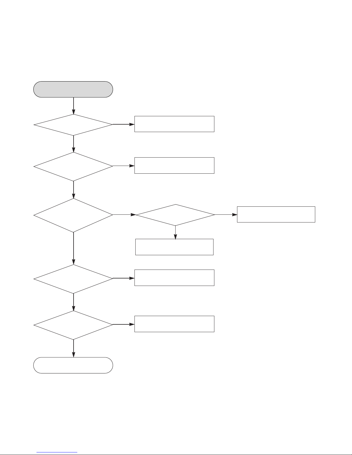
DVD ELECTRICAL TROUBLESHOOTING GUIDE
SECTION 4 DVD PART ELECTRICAL
1. POWER CHECK GUIDE
Power ON
Check DVD MD module.
OK
YES
YES
YES
YES
Does DVD/CD
appear at FLD?
Does
DISK1 appear
at FLD?
Does it
appear DVD ERROR
at FLD?
Func
Power ON
Does
AUX, FM 87.5.AM,
USB appear at
FLD?
YES
Check connector P7501
Check connector
(P400, P4004, P401).
Check an audio micom
or interface reconnect
(P4703)
Does No DISC or
Time are appeared
at FLD?
NO
NO
Check the
voltage of each PIN on
P5701.
NO
NO
NO
NO
YES
OK
Reconnect it.
Page 37

4-2
2. TEST & DEBUG FLOW
Check AV cable
connection to TV set.
Power ON
Check connection lines
between FLASH & ES8380 or
the FLASH access time whether
is suitable or not.
NO NO
YES
Show LOGO?
Flash
memory operates
properly?
Check connection lines
between SDRAM (IC502) &
ES8380 or the SDRAM is
damaged.
NO
YES
SDRAM works
properly?
Check the related
circuit of ES6698FD (IC501)
PIN133,134,137,138,139,140
NO
YES
ES8380
VIDEO outputs
properly?
Check the cable
connection between DVD
PCB and MD (MECHA)
Check the MD mecha
NO NO
YES
Does
tray move
inside when it is at
closed position?
OPEN_SW &
CLOSC_SW signals on
PIN401 are OK
Check the output signal
of ES8380 to IC401 for
control OPEN / CLOSE
NO
YES
OPEN / CLOSE
signals on IC401 are
OK?
Check the tray control
I/O PIN on IC401.
NO
YES
Load+ & load-
signals on P4480
are OK?
YES
YES
B
Page 38

4-3
Do not put in disc
and tray close.
Check the MD
Does
the SLED
move to inner side
when it is at outer
position?
Moter driver DRV-
MMUTE PIN is
high 3
NO
NO
YES
YES
YES
Check the related
circuit of SLED and
motor driver IC (IC401)
SLED
signal is OK?
NO
B
C
Check the cable
connection with MECHA.
Check focus connection on
ES8381 and motor
driver IC.
Optical
Lens is moving
for searching
Focus?
Proper
focus outputs to
motor driver?
NO
NO
YES
YES
YES
YES
Check the motor
driver (IC401).
Proper
F+ & F- outputs?
NO
Check cable connection
with pick-up head.
Page 39

4-4
Put disc in tray. Laser off
Check the laser power circuit
between ES8381 and power
transistor. (Q405, Q406)
Laser
turns on when
reading disc?
DVDLD
or CDLD output
properly?
NO
NO
NO
YES
Check the related circuit of
laser power transistor.
Collector
voltage of power
transistor is OK?
(Q405, Q406)
NO
YES
YES
YES
C
D
Check cable connection
between P400 and
pick-up head.
Check the SPINDLE related
circuit on ES8380
Does SPINDLE
rotate?
Proper
SPINDLE signal
on ES8380.
NO
Check the SPINDLE control
of motor driver (IC404).
SPIN+ &
SPIN- output
properly?
NO
NO
YES
YES
YES
Check the cable
connection between
P400 and MD
Page 40

4-5
Check the connections between
PDM01 and pick-up head.
Check the related circuit of
ES8380 focus signal.
Focus on OK?
Proper
signal on A, B, C, D
from MD?
NO
Proper
FOO signal on
IC401?
NO
NO
YES
YES
YES
D
E
Check cable connection
between P400 and MD.
Check the related circuit
between IC401 and ES8380
Check the tracking control
on motor driver (IC401).
Tracking OK?
Disc play?
Proper
TRO signal on
IC401?
NO
T+ & T- output
properly?
NO
NO
NO
YES
YES
YES
YES
Check cable connection
on pick-up head.
Check RF signal
waveform.
Page 41

4-6
Check the connections between
ES8380 and P4703
All
outputs are OK
during playing
DISK?
Audio
signal data on
P8380 is OK?
NO
NO
YES
YES
E
Check the MAIN PCB
For example composite video,
check the video mute TR
(Q411), output of video buffer
IC (IC407) and ES8380
video signal data
TEST END
Picture
signal data on
ES8380 is OK?
NO
NO
Page 42

4-7
3. USB PART
TURN ON USB
NO
Check the POWER supply circuit.
(Check P5701)
NO
Check the HRST# signal
Check the USB PART and
DVD PART line.
NO
NO
Check the USB DATA LINE. (P5301)
Check the IC501 (ES8380).
(Check DATA LINE PIN 98_USB_NO, 99_PO)
OK
YES
“Checking” or
“USB” display check
NO
YES
Check the USB JACK POWER supply.
(Check P5301)
Reading OK check
NO
Page 43

4-8
WAVEFORMS
1. WHEN POWER ON, RESET & DATA ETC WAVEFORM
1. RESET(DVD)
2. RX
3. TX
4. LCS3# (FLASH)
Playing at USB function
1. HRST#
2. 5V
3. D-
4. D+
Page 44

4-9
2. OPEN / CLOSE WAVEFORM AT POWER ON
1. open
2. UP-sw
3. DOWN-sw
4. close
3. STARTING ACTION WAVEFORM IN MD DEVICE
1. Driver STBY
2. SLEGN
3. SL+
4. SL(At Power on)
Page 45

4-10
4. FOCUS WAVEFORM (AT CD)
1. F+
2. F(NO DISK)
5. FOCUS WAVEFORM (AT DVD)
1.Q401(DVD_LD)
2.Q402(CD_LD)
(INSERT CD)
Page 46

4-11
6. AT POWER ON, SPINDLE SIGNAL AT MD DECK
1. Spind
2. Spin+
3. Spin-
7. AT FIRST ACTION, FOCUS SIGNAL A, B, C, D
1. A
2. B
3. C
4. D
Page 47

4-12
8. TRACKING SIGNAL
1. Tro
2. Tr-
3. Tr+
9. RF WAVEFORM
Page 48

4-13
10. DISK TYPE JUGEMENT WAVEFORM
1. F+
2. FDO
3. SVRRF
(DVD)
(CD)
Page 49

4-14
MEMO
Page 50

4-15 4-16
SCHEMATIC DIAGRAMS
1. MPEG SCHEMATIC DIAGRAM
Page 51

4-17 4-18
2. SERVO SCHEMATIC DIAGRAM
Page 52

3. INTERFACE SCHEMATIC DIAGRAM
4-19 4-20
Page 53

4-21 4-22
DVD P.C.BOARD
(TOP VIEW)
PRINTED CIRCUIT DIAGRAM
Page 54

4-23 4-24
DVD P.C.BOARD
(BOTTOM VIEW)
Page 55

4-25 4-26
MEMO MEMO
 Loading...