

Page 1

MODEL : MDD-K263Q (MDS-K263V)
SERVICE MANUAL
P/NO : AFN62795882
KARAOKE MINI
Hi-Fi SYSTEM
SERVICE MANUAL
CAUTION
BEFORE SERVICING THE UNIT, READ THE “SAFETY PRECAUTIONS” IN THIS MANUAL.
MODEL : MDD-K263Q (MDS-K263V)
Website http://biz.lgservice.com
Internal Use Only
SEPTEMBER, 2008
Page 2

1-1
Copyright © 2008 LG Electronics. Inc. All right reserved.
Only for training and service purposes
LGE Internal Use Only
[CONTENTS]
❍ SECTION 1. GENERAL
• SERVICING PRECAUTIONS ................................................................................................ 1-2
• ESD PRECAUTIONS ............................................................................................................ 1-4
• PROGRAM DOWNLOAD GUIDE.......................................................................................... 1-5
• SPECIFICATIONS ................................................................................................................ 1-6
❍ SECTION 2. EXPLODED VIEWS
• CABINET AND MAIN FRAME SECTION.............................................................................. 2-1
•
MECHANISM EXPLODED VIEW .......................................................................................... 2-3
•
SPEAKER EXPLODED VIEW .............................................................................................. 2-9
• PACKING ACCESSORY
VIEW............................................................................................ 2-10
❍ SECTION 3. ELECTRICAL PART
• TROUBLESHOOTING GUIDE
AUDIO PART TROUBLESHOOTING GUIDE ........................................................................ 3-1
DVD PART TROUBLESHOOTING GUIDE .......................................................................... 3-10
USB PART TROUBLESHOOTING GUIDE .......................................................................... 3-16
• WAVEFORMS OF MAJOR CHECK POINT ........................................................................ 3-17
• WIRING DIAGRAM .............................................................................................................. 3-22
• BLOCK DIAGRAMS ............................................................................................................ 3-23
• CIRCUIT DIAGRAMS .......................................................................................................... 3-25
• INTERNAL BLOCK DIAGRAM OF IC ................................................................................ 3-45
• CIRCUIT VOLTAGE CHART ................................................................................................ 3-59
• PRINTED CIRCUIT DIARGAMS ........................................................................................ 3-65
❍ SECTION 4. REPLACEMENT PARTS LIST ................................................................ 4-1
Page 3
1-2
Copyright © 2008 LG Electronics. Inc. All right reserved.
Only for training and service purposes
LGE Internal Use Only
SERVICING PRECAUTIONS
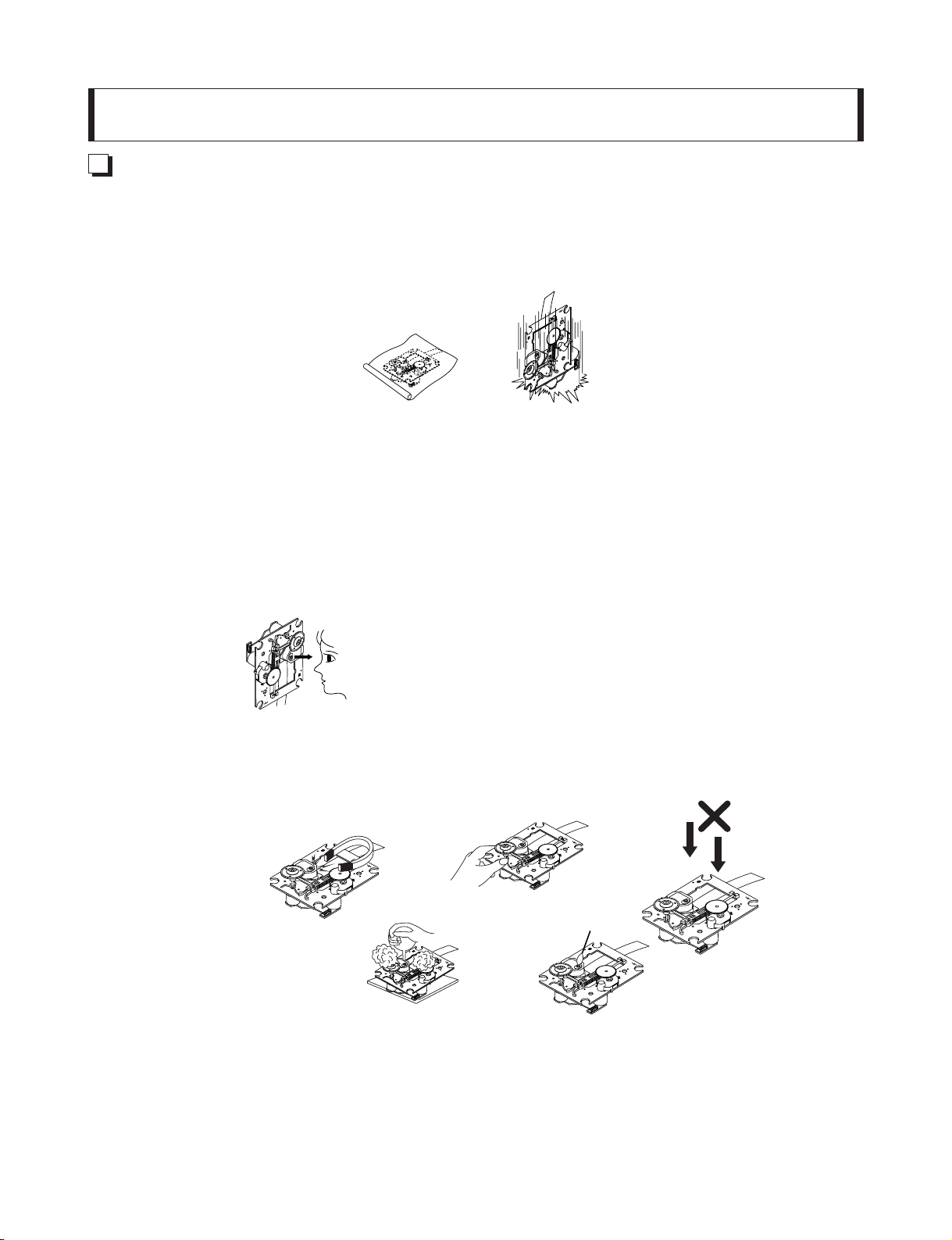
NOTES REGARDING HANDLING OF THE PICK-UP
1. Notes for transport and storage
1) The pick-up should always be left in its conductive bag until immediately prior to use.
2) The pick-up should never be subjected to external pressure or impact.
2. Repair notes
1) The pick-up incorporates a strong magnet, and so should never be brought close to magnetic materials.
2) The pick-up should always be handled correctly and carefully, taking care to avoid external pressure and
impact. If it is subjected to strong pressure or impact, the result may be an operational malfunction and/or
damage to the printed-circuit board.
3) Each and every pick-up is already individually adjusted to a high degree of precision, and for that reason
the adjustment point and installation screws should absolutely never be touched.
4) Laser beams may damage the eyes!
Absolutely never permit laser beams to enter the eyes!
Also NEVER switch ON the power to the laser output part (lens, etc.) of the pick-up if it is damaged.
5) Cleaning the lens surface
If there is dust on the lens surface, the dust should be cleaned away by using an air bush (such as used
for camera lens). The lens is held by a delicate spring. When cleaning the lens surface, therefore, a cotton
swab should be used, taking care not to distort this.
6) Never attempt to disassemble the pick-up.
Spring by excess pressure. If the lens is extremely dirty, apply isopropyl alcohol to the cotton swab.
(Do not use any other liquid cleaners, because they will damage the lens.) Take care not to use too much
of this alcohol on the swab, and do not allow the alcohol to get inside the pick-up.
Storage in conductive bag
Drop impact
NEVER look directly at the laser beam, and don’t allow
contact fingers or other exposed skin.
Magnet
How to hold the pick-up
Conductive Sheet
Cotton swab
Pressure
Pressure
SECTION 1. GENERAL
Page 4
1-3
Copyright © 2008 LG Electronics. Inc. All right reserved.
Only for training and service purposes
LGE Internal Use Only
NOTES REGARDING COMPACT DISC PLAYER REPAIRS
1. Preparations
1) Compact disc players incorporate a great many ICs as well as the pick-up (laser diode). These components
are sensitive to, and easily affected by, static electricity. If such static electricity is high voltage, components
can be damaged, and for that reason components should be handled with care.
2) The pick-up is composed of many optical components and other high-precision components. Care must be
taken, therefore, to avoid repair or storage where the temperature of humidity is high, where strong magnetism is present, or where there is excessive dust.
2. Notes for repair
1) Before replacing a component part, first disconnect the power supply lead wire from the unit
2) All equipment, measuring instruments and tools must be grounded.
3) The workbench should be covered with a conductive sheet and grounded.
When removing the laser pick-up from its conductive bag, do not place the pick-up on the bag. (This is
because there is the possibility of damage by static electricity.)
4) To prevent AC leakage, the metal part of the soldering iron should be grounded.
5) Workers should be grounded by an armband (1M Ω)
6) Care should be taken not to permit the laser pick-up to come in contact with clothing, in order to prevent static electricity changes in the clothing to escape from the armband.
7) The laser beam from the pick-up should NEVER be directly facing the eyes or bare skin.
Resistor
(1 Mohm)
Conductive
Sheet
Resistor
(1 Mohm)
Armband
Page 5

1-4
Copyright © 2008 LG Electronics. Inc. All right reserved.
Only for training and service purposes
LGE Internal Use Only
Electrostatically Sensitive Devices (ESD)
Some semiconductor (solid state) devices can be damaged easily by static electricity. Such components
commonly are called Electrostatically Sensitive Devices (ESD). Examples of typical ESD devices are integrated
circuits and some field-effect transistors and semiconductor chip components. The following techniques should
be used to help reduce the incidence of component damage caused by static electricity.
1. Immediately before handling any semiconductor component or semiconductor-equipped assembly, drain off
any electrostatic charge on your body by touching a known earth ground. Alternatively, obtain and wear a
commercially available discharging wrist strap device, which should be removed for potential shock reasons
prior to applying power to the unit under test.
2. After removing an electrical assembly equipped with ESD devices, place the assembly on a conductive surface
such as aluminum foil, to prevent electrostatic charge buildup or exposure of the assembly.
3. Use only a grounded-tip soldering iron to solder or unsolder ESD devices.
4. Use only an anti-static solder removal device. Some solder removal devices not classified as "anti-static" can
generate electrical charges sufficient to damage ESD devices.
5. Do not use freon-propelled chemicals. These can generate electrical charges sufficient to damage ESD
devices.
6. Do not remove a replacement ESD device from its protective package until immediately before you are
ready to install it. (Most replacement ESD devices are packaged with leads electrically shorted together by
conductive foam, aluminum foil or comparable conductive materials).
7. Immediately before removing the protective material from the leads of a replacement ESD device, touch the
protective material to the chassis or circuit assembly into which the device will by installed.
CAUTION : BE SURE NO POWER IS APPLIED TO THE CHASSIS OR CIRCUIT, AND OBSERVE ALL OTHER
SAFETY PRECAUTIONS.
8. Minimize bodily motions when handing unpackaged replacement ESD devices. (Otherwise harmless motion
such as the brushing together of your clothes fabric or the lifting of your foot from a carpeted floor can generate static electricity sufficient to damage an ESD device).
CAUTION. GRAPHIC SYMBOLS
THE LIGHTNING FLASH WITH APROWHEAD SYMBOL. WITHIN AN EQUILATERAL TRIANGLE, IS
INTENDED TO ALERT THE SERVICE PERSONNEL TO THE PRESENCE OF UNINSULATED
“DANGEROUS VOLTAGE” THAT MAY BE OF SUFFICIENT MAGNITUDE TO CONSTITUTE A RISK OF
ELECTRIC SHOCK.
THE EXCLAMATION POINT WITHIN AN EQUILATERAL TRIANGLE IS INTENDED TO ALERT THE
SERVICE PERSONNEL TO THE PRESENCE OF IMPORTANT SAFETY INFORMATION IN SERVICE
LITERATURE.
SAFETY PRECAUTIONS
Page 6

1-5
Copyright © 2008 LG Electronics. Inc. All right reserved.
Only for training and service purposes
LGE Internal Use Only
PROGRAM DOWNLOAD GUIDE
Caution) Do not perform any other work such as disconnecting USB device, switching to the Function and turning
off the power while downloading it to the set.
The USB device should be disconnected after completing the download.
• AUDIO USB DOWNLOAD GUIDE
1. When the USB device is inserted on the USB function, is displayed on the screen after a while.
“File : MDD263_yymmddx.hex” * x: version.
2. The message “Upgrade” is displayed while downloading.
3. The power is automatically turned off when downloading is completed.
• DVD USB DOWNLOAD GUIDE
The program file to download should be named as BANK.ROM.
- The downloaded file should be modified as BANK30.ROM.
- After safely storing BANK30.ROM at the USB device, perform the following
steps.
1. When the USB device is inserted at the USB function, the screen is changed into downloading
screen.
2. When downloading is completed, the message “Completed” is displayed at the top left on the screen.
3. Turn on the power, press the SETUP button of the remote controller on the USB FUCTION. When the
SETUP window is displayed on the screen, move down once to select the DISPLAY menu. Go to the
TV Aspect on the right menu, move to “16:9”, enter “1397139” by using the numeric key of the remote
controller, and press the Ent er key.
Then, the System Information screen is displayed. If not, retry the steps at the above.
4. When Step 3 is completed, press the Pause key of the remote controller.
5. Disconnect the power cord, and reconnect it after 5 seconds to complete downloading.
6. When the power is turned on, the language selection menu is initially displayed.
After selecting the desired language, press the SELECT/ENTER. ( * not KARAOKE MODEL )
Page 7

1-6
Copyright © 2008 LG Electronics. Inc. All right reserved.
Only for training and service purposes
LGE Internal Use Only
SPECIFICATIONS
General
Power supply Refer to main label.
Power consumption Refer to main label.
Net Weight 6.2 kg
External dimensions (W x H x D) 273 x 326 x 380 mm
Operating conditions Temperature: 5° C to 35° C, Operation status: Horizontal
Operating humidity 5% to 85%
Tuner
FM Tuning Range 87.5 - 108.0 MHz or 65.0 - 74.0 MHz, 87.5 - 108.0 MHz
Intermediate Frequency 10.7 MHz
AM Tuning Range 522 - 1,620 kHz or 520 - 1,720 kHz
Intermediate Frequency 450 kHz
Amplifier
OUTPUT POWER Front: 130 W + 130 W (4 Ω, THD 10 %)
DVD/ VCD/ CD player
Frequency response (audio) 40 - 20000 Hz
Signal- to- noise ratio (audio) More than 75 dB (1 kHz)
Signal- to- noise ratio (video) More than 55 dB (1 kHz)
Dynamic range (audio) More than 80 dB
Video output 1.0 V (p- p), 75 Ω
Component Video output (Y) 1.0 V (p- p), 75 Ω
(Pb)/( Pr) 0.7 V (p- p), 75 Ω
Cassette tape player
F. F/ REW Time 120 sec (C- 60)
Frequency Response 250 - 8000 Hz
Signal to Noise Ratio 43 dB
Channel Separation 45 dB (P/ B)/ 45 dB (R/ P)
Erase Ratio 50dB (MTT- 5511)
Speakers
MDS-K263V
Front Speaker
Type 2Way 3Speaker
Impedance 4 Ω
Rated Input Power 130 W
Max. Input Power 260W
Net Dimensions(W x H x D) 212x 413x 301mm
Net Weight 5.5 kg
Designs and specifications are subject to change without pior notice.
Page 8
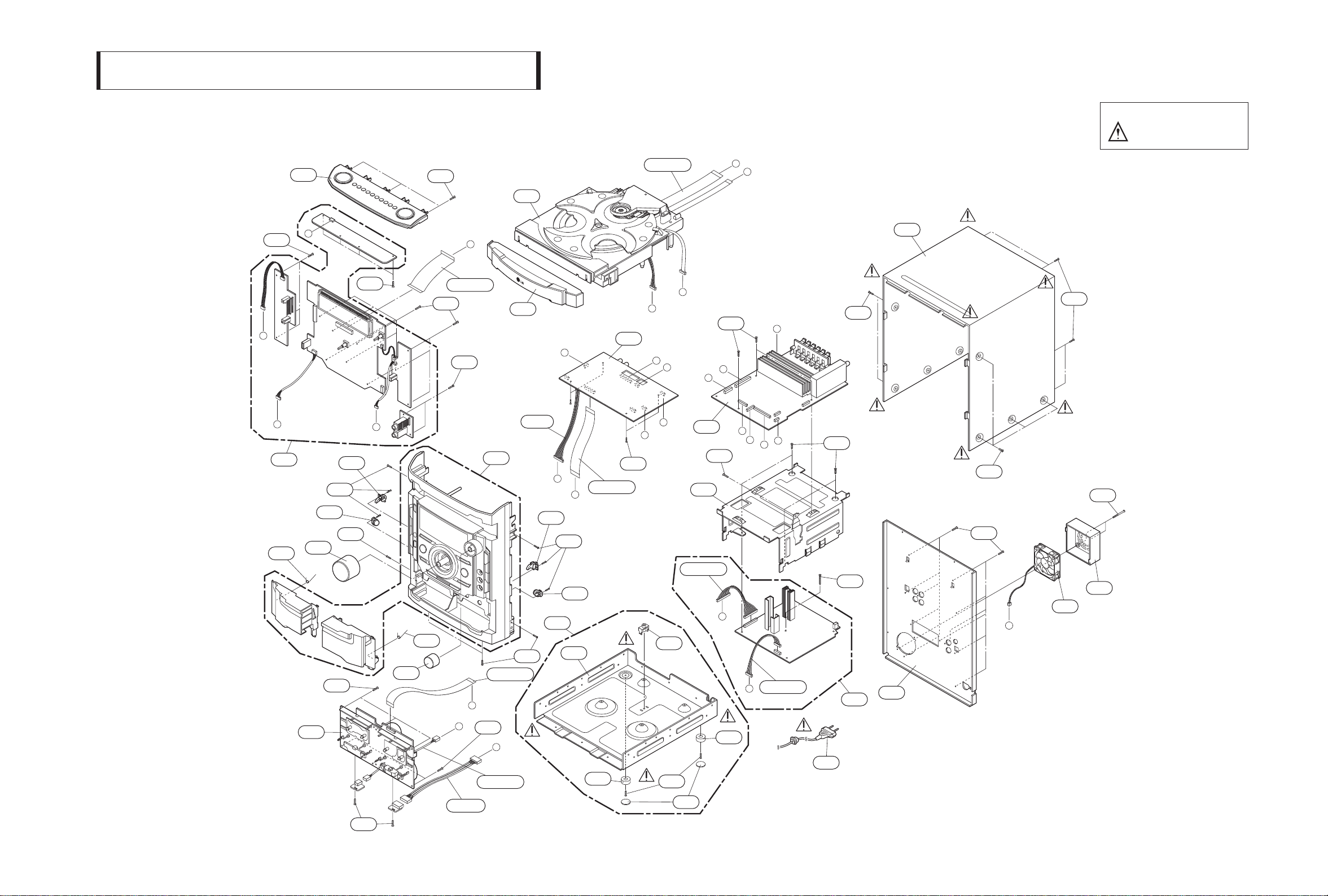
2-1 2-2
Copyright © 2008 LG Electronics. Inc. All right reserved.
Only for training and service purposes
LGE Internal Use Only
• CABINET AND MAIN FRAME SECTION
SECTION 2. EXPLODED VIEWS
252
465
A26
CABLE4
NOTES) THE EXCLAMATION POINT WITHIN AN
EQUILATERAL TRIANGLE IS INTENDED
TO ALERT THE SERVICE PERSONNEL
TO THE PRESENCE OF IMPORTANT
SAFETY INFORMATION IN SERVICE
LITERATURE.
L
K
459
A
KEY2
253
P
A43
A
254
255
465
KEY1
FRONT
256
459
459
459
O
MIC
KEY3
261
253
CABLE3
459
459
H
G
260
251
459
CABLE5
P201
257
A40
J
459
P
255
267
I
A41
DVD
CABLE2
450
266
N
M
465
L
K
N
M
J
A46
D
I
C
MAIN
H
B
O
465
458
465
465
465
264
455
465
CABLE6
289
456
D
SMPS
CABLE7
C
A47
263
B
262
273
A00
465
F
CN201
465
E
CABLE1
290
290
465
291
305
Page 9

2-3 2-4
Copyright © 2008 LG Electronics. Inc. All right reserved.
Only for training and service purposes
LGE Internal Use Only
MECHANISM EXPLODED VIEW
1. TAPE DECK MECHANISM (A/R & A/S : RIGHT A/R DECK)
BRASS MOTOR PULLEY MAYBE CHANGEDFOR WOW FLUTTER WHEN NECESSARY
RING FW MAYBE ADDEDFOR WOW FLUTTER WHEN NECESSARY
RING FW MAYBE ADDEDFOR WOW FLUTTER WHEN NECESSARY
A00
001
002
003
009
011
009
013
A02
015
008
007
006
037
022
023
025
016
017
018
020
A01
019
Page 10

TAPE DECK MECHANISM EXPLODED VIEW
2. TAPE DECK MECHANISM (A/R & A/S : LEFT A/S DECK)
RING FW MAYBE ADDED
FOR WOW FLUTTER WHEN NECESSARY
A00
003
009
011
009
013
A03
015
008
007
022
023
024
016
017
018
020
019
2-5 2-6
Copyright © 2008 LG Electronics. Inc. All right reserved.
Only for training and service purposes
LGE Internal Use Only
Page 11

TAPE DECK MECHANISM EXPLODED VIEW
3. MECHANISM DECK EXPLODED VIEW
2-7 2-8
Copyright © 2008 LG Electronics. Inc. All right reserved.
Only for training and service purposes
LGE Internal Use Only
416
151
159
156 169
422
A26
417
167
416
177
166
164
417
165
440
438
172
175
163
170
419
168
155
162
417
153
173
012A
417
418
169B
169C
430
169A
418
181
A30
430
012A
036
035
180
035A
438
Page 12

2-9
Copyright © 2008 LG Electronics. Inc. All right reserved.
Only for training and service purposes
LGE Internal Use Only
• FRONT SPEAKER (MDS-K263V)
SPEAKER EXPLODED VIEW
A80L
A80R
850
851
853
852
854
A81L
A81R
854
855
856
857
858
860L
860R
861
859
859
Page 13

2-10
Copyright © 2008 LG Electronics. Inc. All right reserved.
Only for training and service purposes
LGE Internal Use Only
• PACKING ACCESSORY
VIEW
808 Battery
900 Remote Control
801 Instruction Ass'y
811
Plug Ass'y, 1Way
Antenna Loop
824
827
825 Antenna
Micro Phone
832
DISC
803 Packing
804 Bag
801S
Song Book
803 Packing
802 Box
Page 14
3-1
Copyright © 2008 LG Electronics. Inc. All right reserved.
Only for training and service purposes
LGE Internal Use Only
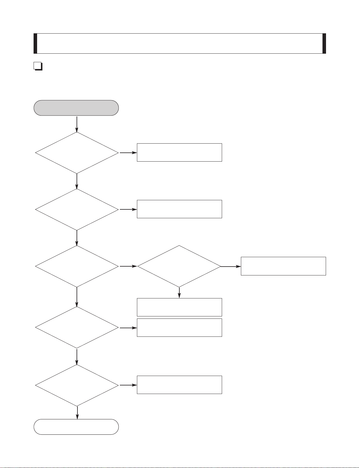
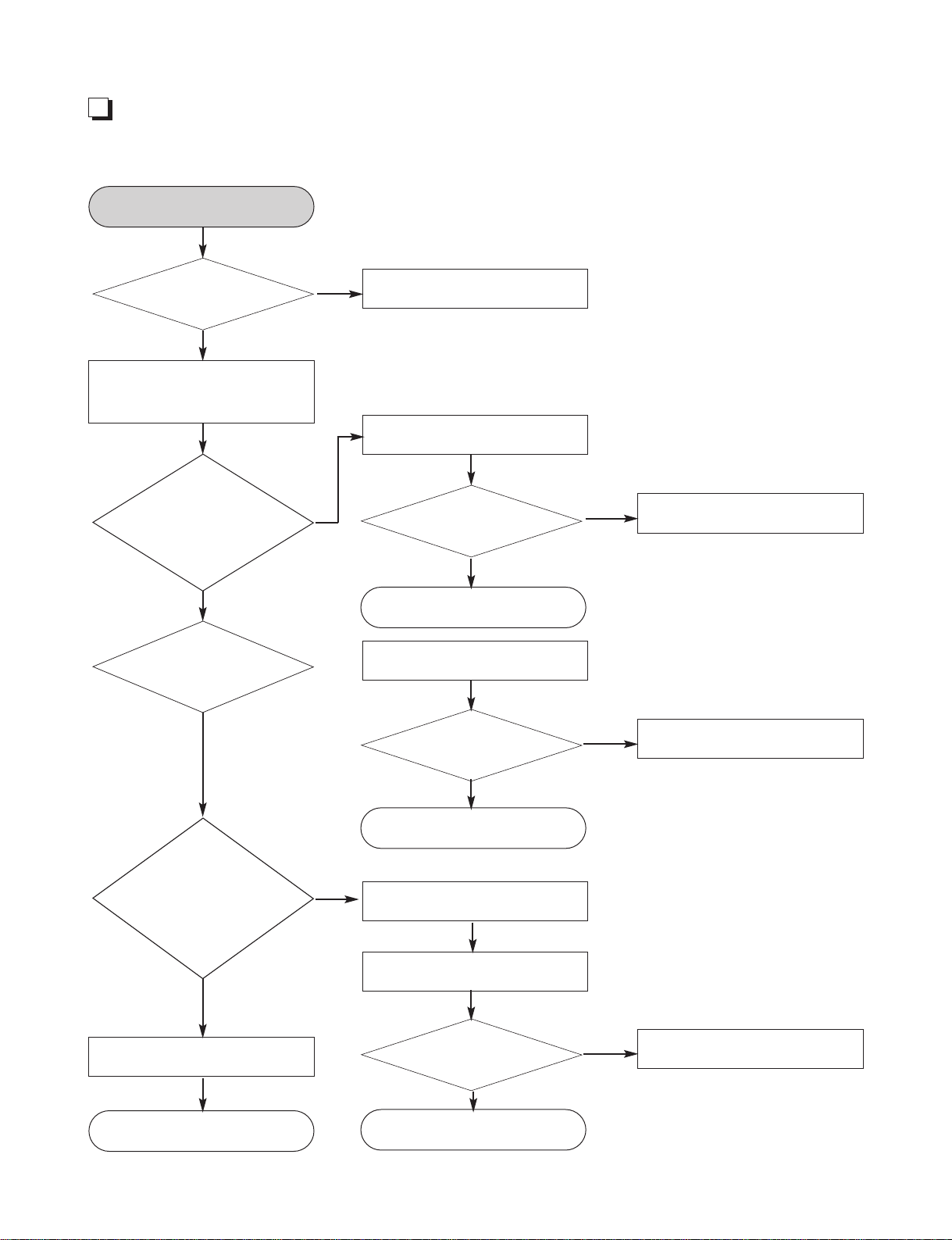
AUDIO ELECTRICAL TROUBLESHOOTING GUIDE
1. POWER (SMPS)
SECTION 3. ELECTRICAL PART
NO
YES
YES
Replace the fuse.
Check the FUSE
F901.
NO
YES
Check BD901,LF901,902.
NO
Check short of P9702 line.
Check short of P9701,P9702 line.
NO
Check short of P9701 line.
NO
Replace IC901,902.
Check
the DC V of C905
if DC V is over
400V.
NO
YES
Check the
DC V of C909,C903,C921
If DC V is in 14~19V
And it is steady
Check IC901,902.
YES
YES
Check the
DC V of C981,C945.
If DC V is 6.1V.
YES
Check the
DC V of C950,C951
If DC V is in
31.68V.
POWER (SMPS)
OK
Page 15

3-2
Copyright © 2008 LG Electronics. Inc. All right reserved.
Only for training and service purposes
LGE Internal Use Only
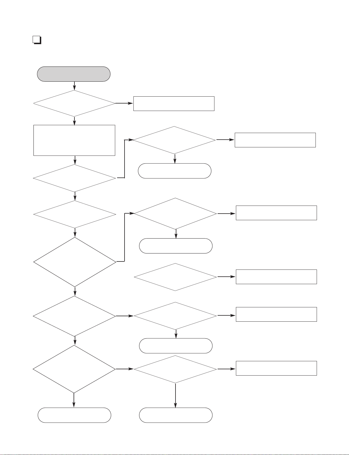
2. P-SENS 3. VKK PART CHECK
4. MICOM PART CHECK I
NO
Check power circuit
Troubleshooting.
YES
P-SENS
Check
the PIN6 of P9702
if DC V is over
5.6V
YES
OK
OK OK
NO
Check power circuit
Troubleshooting.
YES
VKK CHECK
Check
the PIN3 of P9702
if DC V is over
-28V.
YES
OK
NO
NO NO
Replace IC101
(KIA7042)
Check if IC101 of output
voltage is over4.3V
YES
YES
YES YES
YES
Check voltage of
IC100(LC87Fxxx)PIN4
YES
Refer to SMPS
troubleshooting.
MICOM PART
HECK I
Check P-SENS
(P7904_PIN6)
NO
Check both
End voltage of IC101
(KIA7042)
Check
If input voltage of
IC101 is over 5V
Check the
Periphery of IC101
(KIA7042)
AUDIO ELECTRICAL TROUBLESHOOTING GUIDE
Page 16

3-3
Copyright © 2008 LG Electronics. Inc. All right reserved.
Only for training and service purposes
LGE Internal Use Only
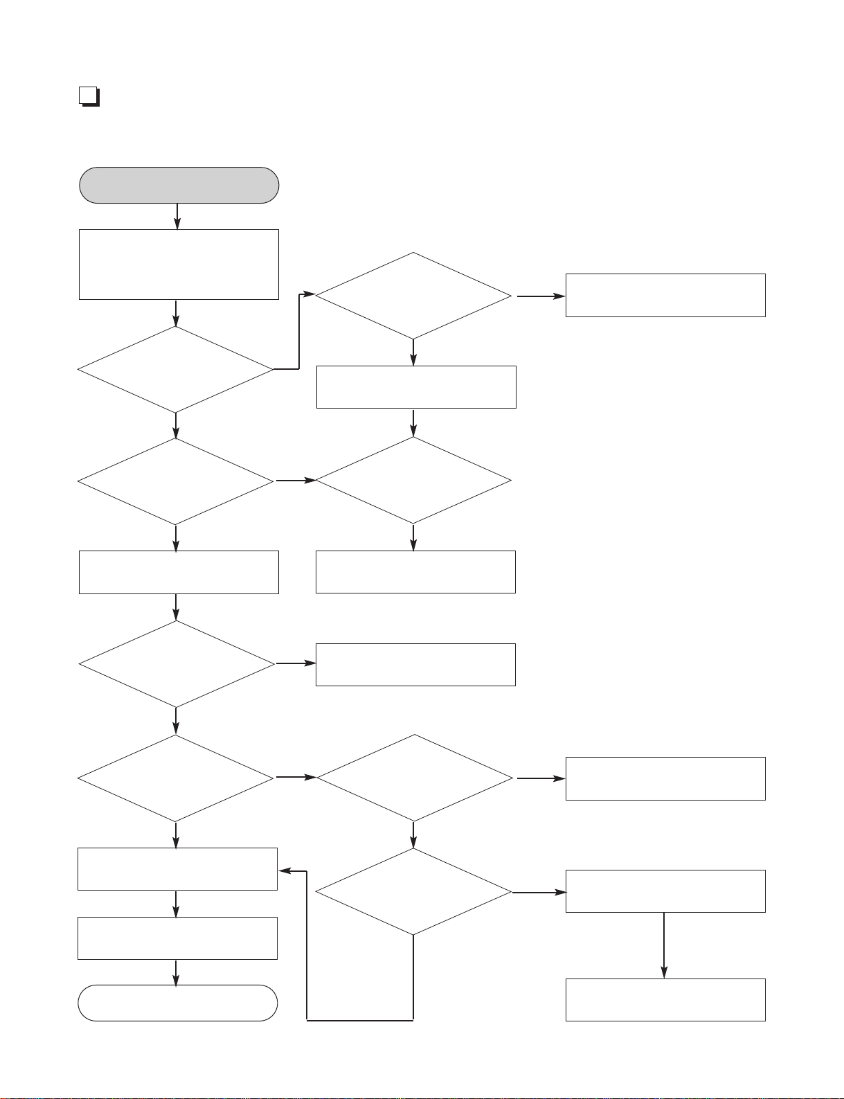
5. MICOM PART CHECK II
6. IC103(S24CS16A01) PART CHECK
NO
NO
YES
YES
YES
YES
YES
YES
YES
Refer to SMPS
troubleshooting.
Check If IC103_PIN8 and
IC100_PIN14,40,55,89 are 5V .
X101:32.768KHz
X100:9.8304MHz
Check the operation.
Check P-SENS
(P7904_PIN6).
Check both
End voltage of D101.
Check
If output of
D101 is 5V.
Check D101.
MICOM PART CHECK II
NO
Replace D101.
OK
OK
YES
YES
YES
YES
PIN81:DATA
PIN82:CLK
Check MICOM.
NO
Check MICOM
Voltage 5V.
CHECK IC100
PIN81,82
NO
Replace MICOM.
NO
Refer to micom
troubleshooting.
OK
OK
AUDIO ELECTRICAL TROUBLESHOOTING GUIDE
Page 17
3-4
Copyright © 2008 LG Electronics. Inc. All right reserved.
Only for training and service purposes
LGE Internal Use Only
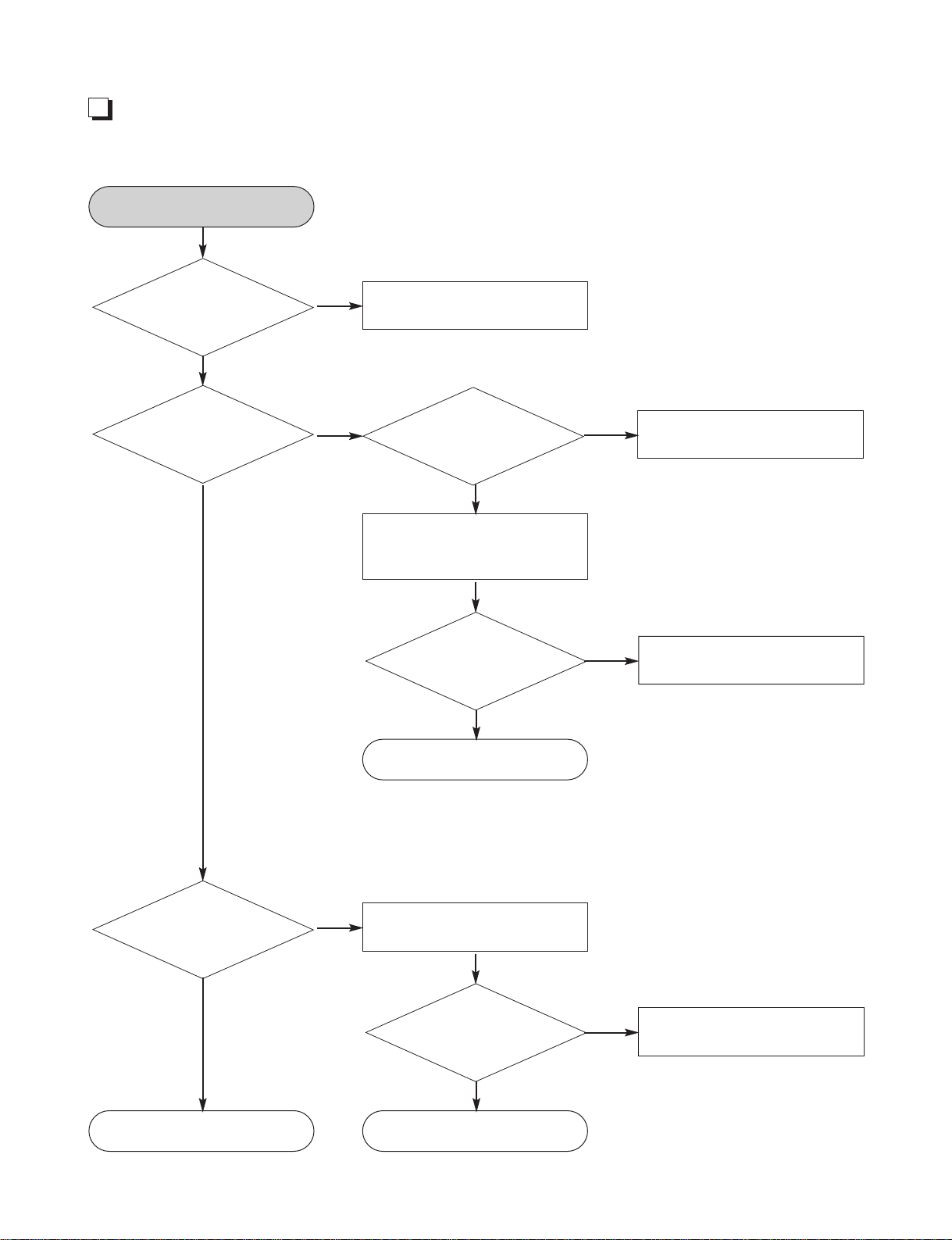
7. FLD DISPLAY PART CHECK
NO
YES
YES
YES
YES
Refer to SMPS.
NO
Replace P3302.
Check P3302 Connection.
Check if both end voltage of
F1,F2 are over 3.7V.
VKK : Over 28V
YES
FLD light on?
Check
P7904 PIN1,2,3
Voltage input
YES
Check P7302
Connection and Power.
pin29:FL+26,pin28:FL-22,
pin27:Vkk over 28V,
pin24:+5.6V
YES
Check
IC301(PT6324)Voltage
Pin50 VKK:-28V
PIN:9,52:+5V
YES
YES
Check each
PIN voltage.
IC100
Check IC301
Data communication.
Pin pin
27pin 3pin STB
26pin 2pin data
28pin 1pin clk
FLD DISPLAY CHECK
OK
OK
OK
NO
Replace IC301.
NO
Replace IC100.
NO
NO
IF voltage is not 5V.
Check input and output of D303.
IC100 : 27,26,28 PIN Check
DATA INPUT.
26PIN DATA OUT
Check DATA INPUT.
YES
YES
YES
Check IC301.
YES
Check IC100.
OK
YES
AUDIO ELECTRICAL TROUBLESHOOTING GUIDE
Page 18
3-5
Copyright © 2008 LG Electronics. Inc. All right reserved.
Only for training and service purposes
LGE Internal Use Only
8. PWM MODULATION PART CHECK
P7905 PIN9,10
3.3V Check
PWM MODULATION
PART CHECK
Refer to SMPS
Troubleshooting
NO
NO
NO
Check
X601 12.288MHz
Operation.
IC604
PIN86 CLK INPUT
Check
Check
IC100(LC87Fxx)
PIN22:PWM REST
PIN79:PWM SDA
PIN80:PWM SCL
OUTPUT
YES
YES
YES
YES
YES
YES
YES
YES
Check
IC604(PS9830)
DATA INPUT PIN23,24,25,26
PWM WAVE
Check.
Check PWM
Modulator output
FL:PIN75(+),74(-)
FR:PIN71(+),70(-)
OTHER OUTPUT
Check
Check IC604(PS9830)
VDD PIN VOLTAGE
(3,10,22,29,39,47,56,65,72,87,94)
Check X601 PIN2 :3.3V
OK
Replace X601.
NO
YES
Check X601
12.288MHz
OK
Replace R671,R670,R665
NO
YES
Check LINE
Resistor output
SDA:R671,SCL:R670
RST:R665
Refer to DVD troubleshooting
NO
Check
DVD ASSY Communication
P7403
Check each LINE
Resistor output
NO
Check
IC604(PS9830) DATA
INPUT
OK
YES
OK
Replace IC604.
NO
Check
IC604(PS9830)
YES
OK
NO
NO
AUDIO ELECTRICAL TROUBLESHOOTING GUIDE
Page 19

3-6
Copyright © 2008 LG Electronics. Inc. All right reserved.
Only for training and service purposes
LGE Internal Use Only
9. PWM MODULATION PART CHECK
YES
YES
NO
Refer to SMPS Troubleshooting.
P7905 PIN3:+12v
PIN13,14,15:32V
YES
YES
NO
Check each line resistor output voltage.
Check each
IC700 PIN1,22,23,44:+12V
INPUT
YES
NO
Replace the coil.
Check output
line coil.
POWER AMP PART CHECK
OK
Check each IC700,701,702,703
PIN27,26,32,35,40,41 INPUT VOLTAGE
YES
Check PWM Modulator input
each PIN6,8,16,18.
YES
POWER IC700
PIN28,31,36,39 output.
AUDIO ELECTRICAL TROUBLESHOOTING GUIDE
Page 20
3-7
Copyright © 2008 LG Electronics. Inc. All right reserved.
Only for training and service purposes
LGE Internal Use Only
10. AUX FUNCTION PART CHECK
OK
Check
IC200 (BU4052)
PIN3,13 each function
output.
Check
IC200 (BU4052)
PIN7:-12V
PIN:16:+12V
Check IC801
(MC4580)
PIN1,7 output.
Check
IC201 (CS5345)
PIN26,27 INPUT.
Check
IC201 (CS5345)
PIN41 data output.
FUNCTION CHECK
Each function
(tuner/tape/portable)
output to IC200(BU4052)
input : L/R_CH.
Check P7501
PIN6(L-CH),PIN8(R-CH).
Each function
output line Check.
Check
IC801 (MC4580)
PIN:-12V
PIN:8:+12V
Check ic201
PIN46:+3.3V
PIN14:+5V
Check ic201
PIN1:SDA
PIN2:SCL
PIN6:RST
Refer to SMPS.
Check CN202 Connection.
IC501(ES8390)
PIN55 INPUT DATA.
IC501(ES8390)
DADATA0 OUTPUT.
Check P7905 connection
After replace IC200.
Check CN202 PIN4,5:+5V
PIN11,12: +3.3V
Check CN206
PIN8:SDA,PIN9:SCL,PIN10:RST
Replace IC201.
YES
YES
YES
YES
YES
YES
YES
YES
YES
YES
YES
YES
YES
YES
YES
NO
NO
NO
NO
NO
NO
NO
AUDIO ELECTRICAL TROUBLESHOOTING GUIDE
Page 21
3-8
Copyright © 2008 LG Electronics. Inc. All right reserved.
Only for training and service purposes
LGE Internal Use Only
11. TUNER/TAPE/PORTABLE FUNCTION PART CHECK
NO
NO
YES
YES
YES
YES
Refer to SMPS troubleshooting.
Check A DECK head input
IC201_PIN32, 39 and B DECK
head input IC201_PIN34, 37.
Check IC210
(HA12237)_PIN16
12V in put.
Check
IC201_ PIN5,
26 signal output.
YES
Check
IC201_PIN14
mute operation.
YES
Check IC201.
Check A/B
DECK head input.
TAPE PLAY PART CHECK
NO
Replace head wire and tape
DECK mechanism.
NO
Replace IC201.
OK
YES
OK
NO
Check IC202_PIN10 "HIGH"
YES
Check IC202.
NO
Replace IC202.
YES
OK
AUDIO ELECTRICAL TROUBLESHOOTING GUIDE
Page 22

3-9
Copyright © 2008 LG Electronics. Inc. All right reserved.
Only for training and service purposes
LGE Internal Use Only
12. TAPE PLAY PART CHECK
NO
NO
Refer to PWM modulation
troubleshooting.
Check
IC604(PS9829)
_PIN49, 52 PWM
output.
Check IC201_
PIN10, 21 output.
Check IC100_
PIN23 "HIGH"
TAPE REC PART CHECK
NO
Replace IC201.
Replace IC202.
Check IC201_PIN7, 24
record input.
YES
OK
NO
Check L203_PIN2, 3
oscillation
Check Q205(D1304)_
base "HIGH"
NO
Check IC202_PIN4 "HIGH".
YES
OK
OK
YES
YES
YES
YES
YES
YES
Check P2203_PIN5, 3inputand
PIN8 erase input.
YES
AUDIO ELECTRICAL TROUBLESHOOTING GUIDE
Page 23

3-10
Copyright © 2008 LG Electronics. Inc. All right reserved.
Only for training and service purposes
LGE Internal Use Only
DVD ELECTRICAL TROUBLESHOOTING GUIDE
1. POWER PART CHECK GUIDE
NO
NO
NO
OK.
NO
NO
Reconnect it.
YES
NO
YES YES
Check an Audio
Micom or interface
reconnect (CN201)
YES
Check DVD MD
Module.
POWER ON
YES
POWER ON
Does
DVD/CD
appear at FLD?
YES
YES
Does No
DISC or Time
are appeared
at FLD?
YES
Check connector
CN701.
Check the
voltage of each pin
on P201.
Does it
appear DVD
ERROR at FLD?
Does
AUX, FM
87.5.AM,USB
appear at
FLD?
Func
Check Connector
(P400,P4004,
P401).
OK
Page 24

3-11
Copyright © 2008 LG Electronics. Inc. All right reserved.
Only for training and service purposes
LGE Internal Use Only
2. TEST & DEBUG FLOW
NO
NO
Check connection lines between
FLASH & ES8390 or the FLASH
access time whether is suitable or not.
YES
Check AV cable connection
to TV set.
Show LOGO?
YESYES
Flash Memory
operates properly?
NO
Check connection lines
between SDRAM (IC502) &
ES8390 or the SDRAM is
damaged.
YES
SDRAM works
properly?
NO
Check the related circuit of
ES8390 (IC501)
PIN133,134,137,138,139,140
YES
ES8390 VIDEO
outputs properly?
NO
NO
Check the MD mecha
Check the cable connection between
DVD PCB and MD (MECHA).
Does tray
move inside when it is
closed position?
YESYES
OPEN_SW&CLOSE_
SW Signals on P401
are OK?
NO
Check the output signal of
ES8390 to IC401 for control
OPEN/CLOSE.
YES
OPEN / CLOSE
signals on IC401 are
OK?
NO
Check the Tray control I/O
Pin on IC401.
YES
Load+ & load- signals
on P4408 are OK?
POWER ON
A
DVD ELECTRICAL TROUBLESHOOTING GUIDE
Page 25

3-12
Copyright © 2008 LG Electronics. Inc. All right reserved.
Only for training and service purposes
LGE Internal Use Only
NO
NO
Check the related circuit of SLED
and Motor driver IC ( IC401)
YES
Check the cable connection
with MECHA.
Do not put in disc
and tray close.
Does the
SLED move to inner side
when it is at outer
position?
YES
YES
YES
SLED signal is OK?
NO
Check the MD
YES
Motor Driver
DRV_MMUTE PINIS
High 3
NO
NO
Check Focus connection on
ES8390 and motor driver IC.
Check cable connection
with pick-up head.
Optical
Lens is moving
for searching Focus?
YESYES
Proper
Focus outputs
to motor driver?
NO
Check the motor driver (IC401).
YES
Proper F+ & F-outputs?
A
B
DVD ELECTRICAL TROUBLESHOOTING GUIDE
Page 26

3-13
Copyright © 2008 LG Electronics. Inc. All right reserved.
Only for training and service purposes
LGE Internal Use Only
NO
NO
NO
Check the laser power circuit between
ES8381 and power transistor.
(Q405, Q406)
YES
YES
Check cable connection
between P400 and pick-up head.
Laser turns on
when reading
disc?
YESYES
DVDLD or CDLD
output properly?
NO
Check the related circuit of laser
power transistor.
YES
Collector
voltage of power transistor
is ok? (Q405, Q406)
NO
NO
Check the SPINDLE related
circuit on ES8390.
Check the cable connection
between P400 and MD.
Does SPINDLE
rotate?
Put disc in tray.
YES
YES
YES
Proper SPINDLE
signal on ES8390.
NO
Check the SPINDLE control of
motor driver (IC404).
SPIN+&SPIN- output
properly?
B
C
DVD ELECTRICAL TROUBLESHOOTING GUIDE
Laser off
Page 27

3-14
Copyright © 2008 LG Electronics. Inc. All right reserved.
Only for training and service purposes
LGE Internal Use Only
NO
NO
Check the connections between
PDM01 and pick-up head.
YES
YES
Check cable connection
between P400 and MD.
Focus On OK?
YESYES
Proper signal on
A,B,C,D from MD?
NO
Check the related circuit of
ES8390 FOCUS signal.
YES
Proper FOD signal on
IC401?
NO
NO
Check the related circuit
between IC401 and ES8390.
Check cable connection on
pick-up head.
Tracking OK?
YES
YES
YES
Proper TRD signal on
IC401?
NO
Check the Tracking control
on motor driver (IC401).
T+ & T- output
properly?
NO
Check RF signal waveform.
Disc play?
C
D
DVD ELECTRICAL TROUBLESHOOTING GUIDE
Page 28

3-15
Copyright © 2008 LG Electronics. Inc. All right reserved.
Only for training and service purposes
LGE Internal Use Only
NO
NO
NO
Check the connections
between ES8390 and CN201.
YES
Check the MAIN PCB.
All
outputs are Ok
during playing
DISK ?
YESYES
Audio signal data on
P8390 is OK?
NO
For example composite video,
Check the video mute TR
(Q507), ES8390
video signal data.
Picture
signal data on
ES8390 is OK?
D
TEST END
Page 29

3-16
Copyright © 2008 LG Electronics. Inc. All right reserved.
Only for training and service purposes
LGE Internal Use Only
1. USB PART
YES
NO
Check the POWER supply circuit.
(Check P201)
Check the HRST # signal.
"Searching" or
"USB" Display check.
YES
YES
Check the USB PART and DVD part line.
YES
NO
Check the USB PART supply.
(Check CN205)
Check the USB DATA LINE. (CN205)
Reading OK check
YES
YES
Check the ES8390.
(Check DATA LINE PIN98_USB_NO, 99_PO)
YES
TURN ON USB
OK
USB ELECTRICAL TROUBLESHOOTING GUIDE
Page 30

3-17
Copyright © 2008 LG Electronics. Inc. All right reserved.
Only for training and service purposes
LGE Internal Use Only
WAVEFORMS OF MAJOR CHECK POINT
1. WHEN POWER ON, RESET & DATA ETC WAVEFORM
1
2
3
1
2
4
1
2
3
4
1
2
IC501
IC501
RESET(DVD)
RX
TX
LCS3# (FLASH)
HRST#
5V
D-
D+
Page 31

3-18
Copyright © 2008 LG Electronics. Inc. All right reserved.
Only for training and service purposes
LGE Internal Use Only
2. OPEN/CLOSE WAVEFORM AT POWER ON
3
1 2
4
1
2
3
4
3. STARTING ACTION WAVEFORM IN MD DEVICE
2
1
1
2
4. FOCUS WAVEFORM (AT CD)
2
1
1
2
open
UP-sw
DOWN-sw
close
SL+
Driver STBY
SLEGN
SL-
F+
F-
Page 32

3-19
Copyright © 2008 LG Electronics. Inc. All right reserved.
Only for training and service purposes
LGE Internal Use Only
5. FOCUS WAVEFORM (AT DVD)
1
2
1
2
6. AT POWER ON , SPINDLE SIGNAL AT MD DECK
1
2
3
1
2
3
7. AT FIRST ACTION, FOCUS SIGNAL A,B,C,D
1
4
3
2
2
1
3
4
Q405(DVD_LD)
Q406(CD_LD)
Spind
Spin+
Spin-
A
B
C
D
Page 33

3-20
Copyright © 2008 LG Electronics. Inc. All right reserved.
Only for training and service purposes
LGE Internal Use Only
8. TRACKING SIGNAL
1
2
3
1
2
3
Tr o
Tr -
9. RF WAVEFORM
1
2
Tr +
Page 34

3-21
Copyright © 2008 LG Electronics. Inc. All right reserved.
Only for training and service purposes
LGE Internal Use Only
3
1
2
10. DISK TYPE JUGEMENT WAVEFORM
1
2
3
DVD CD
F+
F+
FDO
FDO
SVRRF
SVRRF
Page 35

3-22
Copyright © 2008 LG Electronics. Inc. All right reserved.
Only for training and service purposes
LGE Internal Use Only
WIRING DIAGRAM
13P
8P3P
MODULE
AUX
JACK
2 CH SPK TERMINAL
8P
TUNER
3page CHANGER MD
5P
5P
23P
3P
5P
3P
VIDEO
JACK
iPod
JACK
DVD PCB
AUX
JACK
18P
PCB
MAIN
29P
MECHANISM
DOUBLE DECK
FRONT PCB
SMPS PCB
15P
12P
USB MIC H/P
4P
8P
Page 36

3-23
Copyright © 2008 LG Electronics. Inc. All right reserved.
Only for training and service purposes
LGE Internal Use Only
1. MAIN BLOCK DIAGRAM
BLOCK DIAGRAMS
FL
FR
Power
FR +/-
PS9830
AUDIO
Digital
PWM
Modulator
MICOM
N
AMP_PRT, SD, PD
TAS5152orTAS5142
FL +/-
DATA, CLK
PWM_R ST,
K
EEPROM
DATA, CL
M
EEPRO
KS24C021
LC87F5NC8A
P
AM
OPT.
IPOD_DET, RDY
SDRAM
SERIAL
EEPROM
TA
STATIO
N
X
AU
RGB
CVBS
MD
MD
MOTOR
PICK UP
MOTOR
PICK UP
TR +/-, F +/-
SP+/-, SL+/-
LM+/-, TUR+/-
IP9011
MOTOR
DRIVER
A, B, C, D, E, F, RF, MDI, CTL, VR, LDO1/2
DB[0:15]
DMA[0:10]
CS, DI, DO
SPI_ CLK
SDA, SCL
DA_DATA0, 1, 2, 3
MCLK, DA_LRCK, BCK
/CL
SVREF
DRV_MUTE
TRO, FO, SLD
SPO, TUR, OP
MPEG
ES8390
DVD_RST, CS, CLK, DI, DO
5345_RST, CLK, DA
16:9_4:3, RGB_SEL, TV_MODE
FLASH
SCART
O
CVBSY/G, PR/R, PB/B, Y, C
IPOD_VIDE
S/W
VIDEO
MM1225
+6dB
VIDEO
MM1692
SENSOR, OP/CL/UP/DN SW, LIMIT
COMPOSITE
AD_DATA
DOCKING
IPOD
OPTICAL IN
IPOD IN
WITH
6Ch. MUX
IN
MAIN AUDIO
IPOD_RX, TX
Y/G, PR/R, PB/B
AMP
AUX IN
SCART IN
ADC
CS5345
STEREO
/B
D
VFD_STB, DO, CLK
EXP_DATA, CLK
HALL_A/B, LEAF_A
4052_A, B
BT_RST, MPKEY, LE
TA
RDS_CLK, DA
PLL_CLK, DATA, TUNED, STIND
TUNER
TUNER
BU4052
PORTABLE
PT
S/W
AUDIO
IN
IN
BLUETOOTH
AUX
BT /
H/P_L/R
E
PB_MUT
EREC_L/R
HA12237F
TAP
REC L/R
L/R, ERASE
B
DECK
Cassette
REC_MUTE
/B
DECK
TAPE_A
BU2090
MOTOR
SOL_A/B
REC_BIAS
Deck ASP
L/R
A
EXPANDER
D+/D-
MIC SIG.
LC)
PT6324
FLT
DRIVER
BA3308
OPAMP (A
FLT
DECK S/W
DISPLAY
H/P
MIC
USB
Page 37

3-24
Copyright © 2008 LG Electronics. Inc. All right reserved.
Only for training and service purposes
LGE Internal Use Only
2. DVD BLOCK DIAGRAM
P/UP
M
I/F
MICOM
USB CON
I/F
PWM
I/F
POWER
SCI,SDA
EEPROM
DSCK#,CKE,CS0#,RAS0#
DMA[0..11],DB[0..15]
SDRAM
SPI_CS,CLK,DI,KO
SPI
FLASH
DECK MECHANISM
27MHZ
D ,SPINDLE
D ,F ,T
SLE
LOA
3.8V
IC
DRIVE
MOTOR
CD/DVDMDI
CDDVDCT,VRCD,VRDVD
A,B,C,D,E,F,RF
LDO1,LDO2
OPEN/CLOSE
(IP9010)
LRCK,BCK,ADATA[0,3]
CE,CLK,DI,DO, MRST#
USBP, USBN
FOCUS/SLED
AMP_STBY
SPINDLE/TRACKING
MPEG
MPEG
ESS8390 (176PIN)
ESS8390 (176PIN)
3.3V
3.3V
REG
5V
12V
I/F
MIC
(FRONT)
MCLK,BCK
CS5345
MAIN_A
Y,C,Y/G,
Pb/B,
Pr/R
LRCK,DATA
MPEG
Composite
CVBS
MM1692
Composite
Y, Pb, Pr
Component
Page 38

3-25 3-26
CIRCUIT DIAGRAMS
1. SMPS(POWER) CIRCUIT DIAGRAM
2007. 12. 24
A
1
2
3
4
5
6
7
8
9
10
11
12
B C D E F G H I J K L M N O P Q R ST
NOTES) Symbol denotes DC chassis ground.
NOTE) Warning
NOTE) Parts that are shaded are critical
NOTE) With respect to risk of fire or
NOTE) electricial shock.
Copyright © 2008 LG Electronics. Inc. All right reserved.
Only for training and service purposes
LGE Internal Use Only
IMPORTANT SAFETY NOTICE
WHEN SERVICING THIS CHASSIS, UNDER NO CIRCUMSTANCES SHOULD THE ORIGINAL DESIGN BE
MODIFIED OR ALTERED WITHOUT PERMISSION
FROM THE LG CORPORATION. ALL COMPONENTS
SHOULD BE REPLACED ONLY WITH TYPES IDENTICAL TO THOSE IN THE ORIGINAL CIRCUIT. SPECIAL
COMPONENTS ARE SHADED ON THE SCHEMATIC
FOR EASY IDENTIFICATION.
THIS CIRCUIT DIAGRAM MAY OCCASIONALLY DIFFER FROM THE ACTUAL CIRCUIT USED. THIS WAY,
IMPLEMENTATION OF THE LATEST SAFETY AND
PERFORMANCE IMPROVEMENT CHANGES INTO
THE SET IS NOT DELAYED UNTIL THE NEW SERVICE
LITERATURE IS PRINTED.
NOTE :
1. Shaded( ) parts are critical for safety. Replace only
with specified part number.
2. Voltages are DC-measured with a digital voltmeter
during Play mode.
Page 39

3-27 3-38
2. MAIN CIRCUIT DIAGRAM
2008.03.17
A
1
2
3
4
5
6
7
8
9
10
11
12
B C D E F G H I J K L M N O P Q R ST
Copyright © 2008 LG Electronics. Inc. All right reserved.
Only for training and service purposes
LGE Internal Use Only
Page 40

3-29 3-30
3. AMP CIRCUIT DIAGRAM
Copyright © 2008 LG Electronics. Inc. All right reserved.
Only for training and service purposes
LGE Internal Use Only
12
11
10
9
8
7
6
5
4
3
2
1
A
B C D E F G H I J K L M N O P Q R ST
EBY38042101_002.sht
2008.03.17
Page 41

3-31 3-32
4. MPEG CIRCUIT DIAGRAM
Copyright © 2008 LG Electronics. Inc. All right reserved.
Only for training and service purposes
LGE Internal Use Only
12
11
10
9
8
7
6
5
4
3
2
1
A
2008.01.25
B C D E F G H I J K L M N O P Q R ST
Page 42

3-33 3-34
5. SERVO CIRCUIT DIAGRAM
2008.01.25
A
1
2
3
4
5
6
7
8
9
10
11
12
B C D E F G H I J K L M N O P Q R ST
Copyright © 2008 LG Electronics. Inc. All right reserved.
Only for training and service purposes
LGE Internal Use Only
Page 43

3-35 3-36
6. I/O CIRCUIT DIAGRAM
Copyright © 2008 LG Electronics. Inc. All right reserved.
Only for training and service purposes
LGE Internal Use Only
12
11
10
9
8
7
6
5
4
3
2
1
A
2008.01.25
B C D E F G H I J K L M N O P Q R ST
Page 44

3-37 3-38
7. FRONT CIRCUIT DIAGRAM
Copyright © 2008 LG Electronics. Inc. All right reserved.
Only for training and service purposes
LGE Internal Use Only
12
11
10
9
8
7
6
5
4
3
2
1
A
B C D E F G H I J K L M N O P Q R ST
2008.01.25
Page 45

2008.01.25
A
1
2
3
4
5
6
7
8
9
10
11
12
B C D E F G HI
3-39 3-40
8. KEY_1 CIRCUIT DIAGRAM (KARAOKE OPTION) 9. KEY_2 CIRCUIT DIAGRAM
2008.01.25
A
1
2
3
4
5
6
7
8
9
10
11
12
B C D E F G HI
Copyright © 2008 LG Electronics. Inc. All right reserved.
Only for training and service purposes
LGE Internal Use Only
Page 46

3-41 3-42
10. KEY_3 CIRCUIT DIAGRAM 11. MIC CIRCUIT DIAGRAM
Copyright © 2008 LG Electronics. Inc. All right reserved.
Only for training and service purposes
LGE Internal Use Only
2008.01.25
A
1
2
3
4
5
6
7
8
9
10
11
12
B C D E F G HI
2008.01.25
A
1
2
3
4
5
6
7
8
9
10
11
12
B C D E F G HI
Page 47

3-43 3-44
Copyright © 2008 LG Electronics. Inc. All right reserved.
Only for training and service purposes
LGE Internal Use Only
Page 48

3-45
Copyright © 2008 LG Electronics. Inc. All right reserved.
Only for training and service purposes
LGE Internal Use Only
• BU2090
1) BIOCK DIAGRAM
Control circuit
12-bit shift register
Latch
VSS
2
1
3
4
5
6
7
8
DATA
CLOCK
Q0
Q1
Q2
Q3
Q4
16
15
14
13
12
11
10
9
VDD
Q11
Q10
Q9
Q8
Q7
Q6
Q5
Output buffer
(open drain)
Y0
1
Y
2
2
COMMON
Y
3
Y
3
4
Y
1
5
INH
6
V
EE
7
V
SS
8
16
15
14
13
12
11
10
9
V
DD
X2
X1
X
X
0
X3
A
B
Y
0
B
Y
OUT / IN
INH
V
EE
X
OUT / IN
A
COMMON
Y
2
Y3
Y1
X2
X1
X0
X3
INTERNAL BLOCK DIAGRAM OF IC
• BU4052
1) BIOCK DIAGRAM
Page 49

3-46
Copyright © 2008 LG Electronics. Inc. All right reserved.
Only for training and service purposes
LGE Internal Use Only
• ES8390
1) BIOCK DIAGRAM
Motor
OP
U
Motor Driv
DVD/
er
CD
SDRAM
(8/16-MB)
EEPROM
ROM/Flas
deo
ES8390
Vi
Audio
Audi
S/
PDIF
o
TV Display
Speakers
Microphone
A/V Receiver
In
Phoenix II
h
VFD Driver
VFD Panel
IR Remote
Flash Memory Cards / HDD
Page 50

3-47
Copyright © 2008 LG Electronics. Inc. All right reserved.
Only for training and service purposes
LGE Internal Use Only
• HA12237F
1) BIOCK DIAGRAM
RECOUT(L)
21222324252627282930
NC
Test mode
(Open for normal use)
20
IREF
19
GND
EQ
18
+
CC
V
ALC DET
17
REC MUTE OFF/
16
15
ALC
)
High/
A/
MUTE ON/OFF
14
(REC Return ON/OFF
13
12
ALC ON/OFF
11
+
1098
EQ
RECOUT(R)
NC
ALC(L)
RECIN(L)
NC
++
PBOUT(L)
TAI(L)
EQOUT(L)
PB-EQ(L)
PB-NF2(L)
MUTE
93/120
(High/Norm)
+
31
AIN(L)
+
PB-NF1(L)
32
ALC(R)
765432
RECIN(R)
NC
+
PBOUT(R)
MUTE
TAI(R)
EQOUT(R)
93/120
(High/Norm)
BA
Return SW
Return SW
+
BA
1
39
PB-NF1(R)
40
+
RIP
+
33
34
BIN(L)
35
REC-
RETURN
GND
36
37
BIN(R)
38NC
AIN(R)
PB-EQ(R)
PB-NF2(R)
Page 51

3-48
Copyright © 2008 LG Electronics. Inc. All right reserved.
Only for training and service purposes
LGE Internal Use Only
• HA12237F-E
1) BIOCK DIAGRAM
Page 52

3-49
Copyright © 2008 LG Electronics. Inc. All right reserved.
Only for training and service purposes
LGE Internal Use Only
• IP9010
1) BIOCK DIAGRAM
2) PIN CONNECTIONS
Page 53

3-50
Copyright © 2008 LG Electronics. Inc. All right reserved.
Only for training and service purposes
LGE Internal Use Only
• LC87F5NC8AVU-QIP-E
1) BIOCK DIAGRAM
Page 54

3-51
Copyright © 2008 LG Electronics. Inc. All right reserved.
Only for training and service purposes
LGE Internal Use Only
2) PIN ASSIGNMENTS
Page 55

3-52
Copyright © 2008 LG Electronics. Inc. All right reserved.
Only for training and service purposes
LGE Internal Use Only
• 0ILNR00048A
1) BIOCK DIAGRAM
CrOUT
CVBSOUT
YOUT
CYOUT
GND2
CbOUT
COUT
CrIN
VCC
2
5
GND1
CY
IN
15
1
3
Y1IN
BIAS
CbIN
13
11
10
LPF
6.75
MHz
bias
4dB
14
12
9
16
75
Driv
er
2dB
75
Driv
er
8dB
Driver
2dB
Driver
2dB
75
Driv
er
2dB
LPF
6.75
MH
z
clamp
4dB
4
6
7
8
CIN
MU
TE
LPF
13.5
MHz
clamp
4dB
LPF
6.
75MHz
bias
4dB
-6dB
75
Driv
er
2dB
LPF
6.75
MHz
bias
4dB
( TOP VIEW )
VCC
GND1
CYIN C rO
UT
YIN
BIAS
CbIN
CVBSOUT
YOUT
CYOUT
GN
D2
CbOUT
COUT
CrIN
CIN
MUTE
1
2
13
14
15
16
12
11
10
98
7
6
5
4
3
2) PIN CONFIGURATION
Page 56

3-53
Copyright © 2008 LG Electronics. Inc. All right reserved.
Only for training and service purposes
LGE Internal Use Only
PLL
PWM
Modulator
Internal Controls
MLRCK
MBCK
MSDIN[0:3]
SCK/SCL
SO/SDA
SI/I2C_AD0
/CS/I2C_AD
2
PWM2_P/M
PWM3_P/M
PWM4_P/M
PWM5_P/M
PWM6_P
/M
/RESET
OVERLOAD
EXT_MUTE
PWM1_P/M
PWM8_P/M
Internal Clock
SPI/I2C
PWM7_P/M
SLRCK
SBCK
SSDIN[0:3]
PWM_HP_R_P/M
PWM_HP_L_P/M
EPD_ENA
PWM_SWL_P/
M
MIC_LRCK
MIC_BCK
MIC_SDIN
MIC_MC
LK
DMIX_MCLK
OLRCK
OBCK
DMIX_S
DOUT
PLL_DVDD
PLL_DVSS
PLL_AVDD
PLL_AVSS
DVDD
DVSS
IO_VDD
IO_V
SS
Power Supply
Reset & Powe
r Down
Internal Reset
Serial Audio
Output
interfa
ce
Automatic
Gain
Limiter
Main
Volume
Trim
Volume
Bass
Manager
EQ
Down
Mixe
r
Mixe
r
Mic.
Input
Processo
r
Input
Mapper
Sample
Rate
Converte
r
Input
&
Output
MU
X
Host
Interface
(I
2
C, SPI)
Serial
Audio
Output
inter
face
Output Mapper
POP
NR
Crystal
Oscillator
XIN
XO
UT
1
2
3
4
8
7
6
5
OUT2
IN2(-)IN1(+)
Vcc-
Vcc+OUT1
IN1(-)
IN2(+)
• MC4580
1) PIN CONFIGURATION
• PS9830B
1) BIOCK DIAGRAM
Page 57

3-54
Copyright © 2008 LG Electronics. Inc. All right reserved.
Only for training and service purposes
LGE Internal Use Only
2) PIN ASSIGNMENTS
OVERLOAD
EPD_ENA
SO/SDA
SCK/SCL
DVDD
DVSS
SI/I2C_AD0
/CS/I2C_AD2
SPI/I2C
IO_VSS
XIN
XOUT
DMIX_LRCK
DMIX_BCK
DMIX_SDOUT
DVDD
DVSS
_MCLK
DMIX
IO_VDD
IO_VSS
/RESET
TEST_MODE1
TEST_MODE2
SCAN_ENA
TEST_MODE3
IO_VSS
PWM4_P
IO_VSS
PWM8_P
PWM8_M
74
75
6
7
7
7
8
7
9
7
0
8
1
8
8
2
3
8
4
8
8
5
8
6
7
8
8
8
9
8
9
0
1
9
2
9
9
3
4
9
5
9
9
6
7
9
8
9
9
9
0
0
1
1
2
PWM7_P
IO_VDD
71
72
73
PULSUS
3
4
5
PWM7_M
70
6
PWM6_P
IO_VSS
68
69
7
8
PWM6_M
67
9
IO_VSS
IO_VDD
DVDD
66
10111213141516
DVSS
63
64
65
PWM5_P
PWM5_M
61
62
IO_VSS
59
60
171819
PWM4_M
58
IO_VDD
55
56
57
20
2122232425
PWM3_P
PWM3_M
54
PWM2_P
IO_VSS
53
52
PWM2_M
51
50
49
48
47
46
45
44
43
42
41
40
39
38
37
36
35
34
33
32
31
30
29
28
27
26
IO_VSS
PWM1_P
PWM1_M
IO_VDD
PWM_HP_L_P
PWM_HP_L_M
IO_VSS
DVSS
DVDD
PWM_HP_R_P
PWM_HP_R_M
IO_VDD
IO_VSS
PWM_SWL_P
PWM_SWL_M
DVSS
DVDD
MIC_SDIN
MIC_LRCK
MIC_BCK
MIC_MCLK
IO_VDD
IO_VSS
EXT_MUTE
SSDIN3
IO_VSS
PLL_DVSS
PLL_DVDD
IO_VSS
IO_VDD
IO_VDD
MLRCK
MSDIN0
MSDIN1
IO_VSS
IO_VSS
PLL_AVSS
PLL_AVDD
DVSS
DVDD
MBCK
SBCK
MSDIN2
MSDIN3
SLRCK
IO_VSS
SSDIN0
IO_VDD
SSDIN1
SSDIN2
Page 58

3-55
Copyright © 2008 LG Electronics. Inc. All right reserved.
Only for training and service purposes
LGE Internal Use Only
• PT6324
1) BIOCK DIAGRAM
DIN/DOUT
CLK
ST
OSC
LED1
Control
Serial
Data
ace
Interf
B
LED
er
Driv
Display Memory
Timing Genera
Key Matrix Memory
to r
Segment Driver
SG1/KS1
SG2/KS2
SG3/KS3
SG4/KS4
SG5/KS5
SG6/KS6
SG7/KS7
SG8/KS8
SG9/KS9
SG10/KS10
SG11 /KS11
SG12/KS12
SG13/KS13
SG14/KS14
SG15/KS15
SG16/KS16
SG17
SG18
SG19
SG20
SG21
SG22
SG23
SG24
K1 K2
Dimming Circ
uit
VDD GND VEE
Grid
Driv
er
GR1
GR2
GR3
GR4
GR5
GR6
GR7
GR8
GR9
GR1 0
GR11
GR1 2
GR1 3
GR1 4
GR1 5
16
GR
Page 59

3-56
Copyright © 2008 LG Electronics. Inc. All right reserved.
Only for training and service purposes
LGE Internal Use Only
2) PIN CONFIGURATION
GND
VDD
VEE
GR1
GR2
GR4
GR5
GR6
GR7
GR8
GR9
GR3
GR10
CLK
DIN/DOUT
STB
LED1
K1
K2
OSC
GND
VDD
SG1/KS1
SG2/KS2
SG3KS3
SG4/KS4
52 50 49 48
1
2
3
4
5
6
7
8
9
10
11
12
13
14
16
47
PT6324
18 19 20
17
46 45
21 22
44
43
23
42 41
25 2615
24
4051
39
38
37
36
35
34
33
32
31
30
29
28
27
GR11
GR12
GR13
GR14
GR15
GR16
SG24
SG23
SG22
SG21
SG20
SG19
SG18
SG17
SG6/KS6
SG7/KS7
SG8/KS8
SG5/KS5
SG9/KS9
SG11/KS11
SG10/KS10
SG12/KS12
SG14/KS14
SG13/KS13
SG15/KS15
SG16/KS16
Page 60

3-57
Copyright © 2008 LG Electronics. Inc. All right reserved.
Only for training and service purposes
LGE Internal Use Only
• TAS5352
1) BIOCK DIAGRAM
2nd-Order L-C
Output Filter
for Each
Half-Bridge
Bootstrap
Capacitors
2-Channel
H-Bridge
BT
L
Mode
System
Microcontroller
OUT_
A
OUT_
B
OUT_
C
OUT_
D
BST_A
BST_B
BST_C
BST_D
RESET_A
B
RESET_CD
System
Power
Supply
Hardwire
Mode
Control
PVDD
GVDD (12 V)/VDD (12 V)
GND
Hardwire
OC Limit
M1
M3
PVDD
Power
Supply
Decoupling
35.5 V
12
V
GND
VAC
PWM_A
PWM_C
PWM_D
PWM_B
V
ALID
M2
Left-
Channel
Output
Right-
Channel
Output
Inpu
t
H-Bridge 1
Inpu
t
H-Bridge 2
GVDD
VDD
VREG
Power Supply
Decoupling
44 4
Bootstra
p
Capacitors
2nd-Order L-C
Output Filter
for Each
Half-Bridge
Output
H-Bridge 2
Output
H-Bridge
1
OTW
OTW
SD
SD
TAS5518
PVDD_A, B, C, D
GND_A, B, C, D
GVDD_A, B, C, D
GND
VDD
VREG
AGND
OC_ADJ
Page 61

3-58
Copyright © 2008 LG Electronics. Inc. All right reserved.
Only for training and service purposes
LGE Internal Use Only
Page 62

3-59 3-60
Copyright © 2008 LG Electronics. Inc. All right reserved.
Only for training and service purposes
LGE Internal Use Only
CIRCUIT VOLTAGE CHART
IC MAIN
IC 100 (audio Micom) LC87F5NC8A
1 1.31
2 0.35
3 0.21
4 3.81
5 0.86
6 1.09
7 4.44
8 5.02
9 2.34
10 2.54
11 0.01
12 2.45
13 2.55
14 5.07
15 5.02
16 4.98
17 4.99
18 4.9
19 0.01
20 0.9
21 0.83
22 4.98
23 0.02
24 0.23
25 3.37
26 5.03
27 5.03
28 5.03
29 4.64
30 0.01
31 0.01
32 0.01
33 0.01
34 5.03
35 0.01
36 5.03
37 0.01
38 5.04
39 0.01
40 5.04
41 0.32
42 0.39
43 0.01
44 0.01
45 0.01
46 4.95
47 0.23
48 0.27
49 0.26
50 0.28
51 0.3
52 0.28
53 0.39
54 5.02
55 5.04
56 0.01
57 0.81
58 0.02
59 0.01
PIN NO.
60 0.01
61 0.21
62 0.29
63 0.57
64 0.64
65 2.03
66 2.08
67 2.09
68 2.14
69 0.01
70 5.52
71 5.01
72 3.23
73 3.9
74 2.04
75 2.12
76 2.11
77 5.04
78 5.04
79 5.01
80 5.01
81 5.04
82 5.04
83 4.22
84 0.01
85 0.02
86 2.82
87 0.07
88 0.01
89 5.04
90 0.12
91 0.12
92 0.1
93 0.03
94 2.27
95 2.08
96 4.74
97 4.82
98 0.01
99 0.01
100 0.01
IC 604 Pulsus (PS9830)
1 0.001
2 0.001
3 1.93
4 3.46
5 0.001
6 1.95
7 0.001
8 0.001
9 0.001
10 3.44
11 1.79
12 1.8
13 1.9
14 0.001
15 0.03
16 1.69
17 1.68
18 1.76
19 1.68
VOLT
PIN NO.
VOLT
PIN NO.
VOLT
PIN NO.
VOLT
EE Mode (V)
EE Mode (V)
EE Mode (V)
EE Mode (V)
20 1.71
21 0.001
22 3.44
23 0.02
24 0.02
25 0.02
26 0.02
27 0.001
28 0.001
29 3.44
30 1.67
31 1.71
32 1.71
33 0.01
34 1.9
35 0.001
36 1.71
37 1.71
38 0.001
39 3.44
40 1.71
41 1.71
42 1.9
43 0.001
44 0.001
45 1.71
46 1.71
47 3.44
48 1.71
49 1.71
50 0.001
51 1.71
52 1.71
53 0.001
54 1.71
55 1.71
56 3.44
57 0.001
58 1.71
59 1.71
60 0.001
61 1.71
62 1.71
63 0.002
64 0.001
65 3.44
66 1.9
67 1.71
68 1.71
69 0.001
70 1.71
71 1.71
72 3.44
73 0.001
74 1.71
75 1.71
76 3.37
77 3.44
78 4.98
79 4.98
80 1.9
81 0.002
82 0.002
83 0.002
84 0.002
85 0.002
86 1.71
87 1.76
88 1.69
89 1.68
90 1.68
91 1.9
92 0.002
93 1.66
94 3.44
95 0.002
96 5.01
97 0.002
98 0.002
99 0.002
100 0.002
PIN NO.
EE Mode (V)
IC 200 (BU4052)
1 0.01
2 0.01
3 0.01
4 0.01
5 0.01
6 0.01
7 -6.29
8 0.01
9 0.01
10 0.01
11 0.01
12 0.01
13 0.01
14 0.01
15 0.01
16 5.96
IC801 (MC4580)
1 0.06
2 0.04
3 0.04
4 -12.23
5 0.04
6 0.06
7 0.06
8 11.58
IC802 (MC4580)
1 0.01
2 0.01
3 0.03
4 -11.28
5 0.03
6 0.02
7 0.01
8 11.26
IC601 (MSGEQ7N)
1 5.14
2 0.01
3 0.4
38 1.5
39 0.04
40 1.19
41 3.4
42 3.4
43 3.19
44 3.19
45 3.29
46 0.96
47 0.65
48 3.4
49 0.09
50 4.08
51 0.01
52 3.35
53 4.87
54 3.37
55 1.69
56 1.65
57 1.7
58 1.65
59 3.38
60 3.38
61 0.01
62 3.38
63 3.38
64 1.36
65 3.38
66 3.38
67 0.01
68 1.5
69 3.37
70 3.38
71 1.65
72 4.29
73 1.8
74 0.01
75 3.35
76 0.02
77 2.36
78 1.31
79 3.38
80 0.94
81 3.35
82 0
83 0.93
84 0.9
85 0.76
86 3.36
87 3.4
88 0.01
89 3.4
90 0.02
91 0.02
92 0.59
93 1.08
94 1.09
95 0
96 1.69
97 0.02
98 0.02
99 3.37
100 0.01
101 0.02
102 0.02
103 1.68
104 1.5
105 1.81
106 1.75
107 0.01
108 3.35
109 0.01
110 0.02
111 3.37
112 0.01
113 3.38
114 0.01
115 3.36
116 0.01
117 0.63
118 0.56
119 1.97
120 1.65
121 1.95
122 1.7
123 0.08
124 1.29
125 3.4
126 3.41
127 2.14
128 1.54
129 0.59
130 3.29
131 0.09
132 0.5
133 3.37
134 0.02
135 1.7
136 1.7
137 1.88
138 1.88
139 1.88
140 1.88
141 1.84
142 1.84
143 2.13
144 2.14
145 1.65
146 0.02
147 1.71
148 1.71
149 1.71
150 1.73
151 1.35
152 3.37
153 0
154 0
155 1.53
156 3.35
157 0
158 1.5
159 1.23
PIN NO.
EE Mode (V)
4 0.04
5 2.2
6 2.58
7 0.08
8 2.54
IC103(S24CS1)
1 0.01
2 0.01
3 0.01
4 0.01
5 5.04
6 5.04
7 0.01
8 5.04
IC102(KIA70)
1 5.04
2 0.01
3 5.03
IC101(KIA70)
1 5.23
2 0.01
3 4.08
IC DVD
IC 501 Mpeg (ES8390)
1 3.37
20
3 0.22
4 3.26
5 3.2
6 3.3
7 3.46
80
9 1.45
10 0.02
11 0.92
12 0.94
13 0.86
14 3.35
15 0
16 1.5
17 0.71
18 0.91
19 0.71
20 0.71
21 0.6
22 0.83
23 0.89
24 0.77
25 0.76
26 0.68
27 0.87
28 0.95
29 0
30 3.35
31 1.11
32 3.35
33 1.17
34 0.42
35 0.29
36 3.35
37 0.02
Page 63

3-61 3-62
Copyright © 2008 LG Electronics. Inc. All right reserved.
Only for training and service purposes
LGE Internal Use Only
PIN NO.
EE Mode (V)
160 1.23
161 1.38
162 1.53
163 3.47
164 0
165 1.79
166 1.38
167 2.62
168 0
169 0.02
170 1.6
171 0.56
172 0.55
173 0.09
174 0.09
175 0.03
176 0.09
PIN NO.
PB Mode (V)
IC 501 Mpeg (ES8390)
1 3.36
20
14 3.36
15 0
29 0
30 3.36
36 3.36
37 0
38 1.51
51 0
52 3.36
66 3.36
67 0
68 1.51
72 4.31
74 0
75 3.36
81 3.4
82 0
87 3.25
88 0
89 3.4
95 0
99 3.36
100 0
104 1.51
107 0
108 3.36
115 3.35
116 0
122 1.7
127 2.15
133 3.35
134 0
153 0
154 0
155 1.51
156 3.36
157 0
158 1.51
163 3.36
PIN NO.
PB Mode (V)
164 0
IC401 (IP9011)
1 2.12
2 2.16
3 2.05
4 2.18
5 4.9
6 1.72
7 1.71
GND 0
8 3.29
9 1.08
10 0
11 0
12 4.89
13 0.21
14 0.21
15 3.39
16 0.826
17 2.08
18 2.18
19 4.9
20 1.72
21 1.41
GND 0
22 0
23 1.7
24 0.16
25 0
26 1.23
27 2.21
28 1.56
PIN NO.
EE Mode (V)
IC401 (IP9011)
1 0.12
2 0.11
3 0.1
4 0.09
5 4.97
6 1.7
7 1.71
GND 0
8 0.02
9 1.09
10 0
11 0
12 4.97
13 0.09
14 0.09
15 0.04
16 0.36
17 0.11
18 0.11
19 4.97
20 1.7
21 1.7
GND 0
22 0
23 1.7
24 0.08
PIN NO.
EE Mode (V)
25 0
26 1.28
27 2.21
28 1.56
IC502
1 3.39
2 0.6
3 3.39
4 0.71
5 0.71
60
7 0.91
8 0.71
9 3.38
10 0.86
11 0.94
12 0
13 0.92
14 3.38
15 0.02
16 0
17 3.3
18 3.2
19 3.26
20 0.09
21 0.03
22 0.09
23 0.09
24 0.55
25 0.56
26 1.6
27 3.38
28 0.01
29 1.38
30 1.53
31 1.79
32 1.38
33 2.62
34 0
35 0.02
36 0.02
37 3.38
38 1.45
39 0.02
40 0
41 0.01
42 0.83
43 3.38
44 0.89
45 0.77
46 0.01
47 0.76
48 0.68
49 3.39
50 0.87
51 0.95
52 0.01
53 1.11
54 0.01
IC503
1 3.16
PIN NO.
EE Mode (V)
2 1.65
3 3.4
4 0.01
5 0.63
6 2.51
7 3.4
8 3.41
IC504
1 0.01
2 0.01
3 0.01
4 0.01
5 0.19
6 3.47
70
8 3.48
IC TIMER
IC303
1 4.77
2 3.82
3 3.76
4 2.18
5 0.05
6 0.05
7 2.84
80
9 5.06
10 -9.79
11 -19.5
12 0.019
13 -21.2
14 -21.22
15 -19.59
16 -24.62
17 -24.62
18 -21.23
19 -19.51
20 -21.14
21 -24.48
22 -19.59
23 -17.92
24 -24.55
25 -24.62
26 -24.78
27 -24.76
28 -24.74
29 -24.77
30 -24.78
31 -24.79
32 -24.77
33 -24.8
34 -23.33
35 -23.29
36 -23.28
37 -23.28
38 -23.28
39 -23.28
40 -23.29
41 -23.29
42 -23.28
43 -23.28
PIN NO.
EE Mode (V)
44 -23.29
45 -23.3
46 -23.27
47 -23.27
48 -23.27
49 -24.92
50 -24.98
51 5.06
52 0
IC301
10
20
30
4 3.85
5 0.6
6 0.61
7 4.96
8 0.48
9 0.12
10 0.09
11 0.01
12 4.85
13 4.44
14 4.46
15 0.09
16 5.53
IC302
1 1.76
2 0.003
3 1.76
40
50
6 10.21
7 1.76
8 0.017
9 1.76
Page 64

3-63 3-64
Copyright © 2008 LG Electronics. Inc. All right reserved.
Only for training and service purposes
LGE Internal Use Only
AUDIO MAIN
NO VALUE CAPACITOR (UF)
VOLTAGE_SPEC POSITIP (+) NEGATIP (-) GAP MARGIN
C109 220 10V 5.09V 0.006V 5.084V 4.916V
C111 100 10V 5.01 0.006 5.004V 4.996V
C116 2.2 50V 5.09V 0.006V 5.084V 44.916V
C635 10 16V - - 16V
C639 10 16V 1.92V 0.001V 1.919V 14.081V
C647 1000 6.3V 3.44 0.001 3.439V 2.57V
C665 470 10V 1.9 0.01 1.89V 8.11V
C690 100 16V - - 16V
C803 4.7 50V 2.48V 0.54V 1.94V 48.06V
C805 4.7 50V 2.49V 0.52V 1.97V 48.03V
C810 47 16V 0V -12.21V 12.21V 3.79V
C811 47 16V 11.48V 0V 11.48V 4.52V
C814 10 16V - - 16V
C815 47 16V - - 16V
C818 10 16V 1.41V 0V 1.41V 14.59V
C824 47 16V - - 16V
C825 10 16V 5.92V 0V 5.92V 10.08V
C827 10 50V 0V -6.29V 6.29V 43.71V
C840 100 16V - - 16V
C846 220 10V 0 0 10V 0V
C848 220 10V 0.002V 0.001V 0.001V 9.999V
C852 10 16V 1.7 0.026 1.674V 14.326V
C853 10 16V 1.7 0.025 1.675V 14.326V
C859 10 16V 1.7 0.024 1.676V 14.324V
C862 220 10V - - 10V
C725 10 50V 11.84V 0.001V 11.839V 38.161V
C707 47 50V 11.82V 0.001V 11.819V 38.181V
C836 220 16V 9.63V 0.001V 9.629V 6.371V
C741 1000 50V 34.51V 0.008V 34.502V 15.498V
C703 1000 50V 34.5V 0.007V 34.493V 15.507V
DVD MAIN
NO VALUE CAPACITOR (UF)
VOLTAGE_SPEC POSITIP (+) NEGATIP (-) GAP MARGIN
C409 100 16V 4.99V 0.02V 4.97V 11.03V
C408 100 16V 4.99V 0.02V 4.97V 11.03V
C512 47 6.3V 3.38V 0.02V 3.36V 2.64V
C511 220 10V 3.38V 0.02V 3.36V 6.64V
C517 100 16V 3.4V 0.02V 3.38V 12.62V
C515 10 16V 3.4V 0.02V 3.38V 12.62V
C406 47 6.3V 2.1V 0.02V 2.08V 4.22V
C401 47 6.3V 4.99V 0.02V 4.97V 1.03V
C405 4.7 6.3V 4.99V 0.02V 4.97V 1.33V
C404 100 16V 4.99V 0.02V 4.97V 11.03V
C410 100 16V 3.42V 3.41V 0.01V 15.99V
C407 100 16V 3.42V 3.41V 0.01V 15.99V
C510 100 16V 3.42V 0.01V 3.41V 12.59V
C516 100 16V 3.42V 0.01V 3.41V 12.59V
C500 100 16V 1.52V 0.02V 1.5V 14.5V
C5C5 10 16V 1.11V 0.01V 1.1V 14.9V
C5C4 10 16V 1.11V 0.01V 1.1V 14.9V
C231 47 6.3V 3.43V 0.02V 3.41V 2.89V
C232 47 6.3V 4.98V 0.01V 4.97V 1.33V
C242 10 16 2.49V 0.01V 2.48V 13.52V
C241 47 6.3V 4.97V 0.01V 4.96V 1.34V
C223 10 16V 2.5V 0.01 2.49V 13.51V
C230 47 6.3V 5V 0.01 4.99V 1.31V
C224 47 6.3V 0.95 0.95 0V 6.3V
TIMER
NO VALUE CAPACITOR (UF)
VOLTAGE_SPEC EEMODE
POSITIP (+) NEGATIP (-) GAP MARGIN
C323 1 50V 0V 0V 0V 50V
C334 100 16V 10.19V 0V 10.19V 5.81V
C341 100 16V 5.05V 0V 5.05V 10.95V
C315 22 16V 1.785V 0V 1.785V 14.215V
C351 47 16V 11.81V 0V 11.81V 4.19V
C327 47 35V 0V -21.53V 21.53V 13.47V
C338 47 35V 0V -25.03V 25.03V 9.97V
C348 47 35V 0V -17.79V 17.79V 17.21V
C377 100 10V 4.94V 0V 4.94V 5.06V
C382 1 50V 0V 0V 0V 50V
C383 1 50V 0V 0V 0V 50V
Page 65

3-65 3-66
Copyright © 2008 LG Electronics. Inc. All right reserved.
Only for training and service purposes
LGE Internal Use Only
PRINTED CIRCUIT BOARD DIAGRAMS
1. MAIN P.C. BOARD DIAGRAM ( TOP VIEW )
Page 66

3-67 3-68
Copyright © 2008 LG Electronics. Inc. All right reserved.
Only for training and service purposes
LGE Internal Use Only
MAIN P.C. BOARD DIAGRAM ( BOTTOM VIEW )
Page 67

3-69 3-70
Copyright © 2008 LG Electronics. Inc. All right reserved.
Only for training and service purposes
LGE Internal Use Only
2. DVD P.C. BOARD DIAGRAM ( TOP VIEW )
Page 68

3-71 3-72
Copyright © 2008 LG Electronics. Inc. All right reserved.
Only for training and service purposes
LGE Internal Use Only
DVD P.C. BOARD DIAGRAM ( BOTTOM VIEW )
Page 69

3-73 3-74
Copyright © 2008 LG Electronics. Inc. All right reserved.
Only for training and service purposes
LGE Internal Use Only
3. SMPS P.C. BOARD DIAGRAM
NOTE: Warning
Parts that are shaded are critical With
respect to risk of fire or electrical shock.
Page 70

3-75 3-76
Copyright © 2008 LG Electronics. Inc. All right reserved.
Only for training and service purposes
LGE Internal Use Only
4. FRONT P.C. BOARD DIAGRAM
EAX42692302
EAX42692302
EAX42692302
Page 71

3-77 3-78
EAX42692702
EAX42692902
EAX42692802
EAX42692602
Copyright © 2008 LG Electronics. Inc. All right reserved.
Only for training and service purposes
LGE Internal Use Only
5. KEY_1 P.C. BOARD DIAGRAM (KARAOKE OPTION) 6. KEY_2 P.C. BOARD DIAGRAM
8. MIC P.C. BOARD DIAGRAM7. KEY_3 P.C. BOARD DIAGRAM
KEY1
KEY1
EAX42692702
EAX42692702
EAX42692802
EAX42692802
EAX42692902
EAX42692902
EAX42692602
EAX42692602
 Loading...