

LG MD120 Service Manual
Z3X-BOX.COM

y
Table Of Contents
1.INTRODUCTION
1.1 Purpose ........................... .. .................................................................. .................................. 3
1.2 Regulatory Information............................................................................ ..............................3
1.3 Abbreviations .................................................... ........................... ........................... ...............6
2..Circuit Description
2.1 RF Transmit/Receive Part...... ... ..................................................... ......... ...............................8
2.2 Description of Receive Part Circuit......................................................... .............................10
2.3 Description of Transmit Part Circuit…………………………………...................……......11
2.4 Description of Frequency Synthesizer Circuit……………………...................………... ...14
2.5. Digital/Voice Processing Part………………………………………...................……..….14
2.6 Configuration………………………………………………...................……………..…...14
2.7 Briefly Circuit Description……………………………………....................………….…...15
2.8 Power Supply Part…………………………………………………...................……..……17
2.9 Logic Part…………………………………………………...................………………..….18
3. TROUBLE SHOOTING
3.1 RF Component............................................................................ .........................................21
3.2 RX Trouble.............................................................................. .............................................22
3.3 TX Trouble ........... ............. ....... ......... ......... ...... ......... ......... ....... .......... ....... ......... ................28
3.4 Power On Trouble....................................................................... .........................................35
3.5 Charging Trouble .................................................................. ...............................................37
3.6 V ibrator T rouble ....................................................... ...........................................................39
3.7 LCD Trouble........................................................................... .............................................40
3.8 Speaker Trouble .................................................................. .................................................43
3.9 Earphone Trouble ..... . .............................................................. ............................................45
3.10 KEY backlight Trouble .................................................. ...................................................47
3.11 ReceiverTrouble………………………………………………………..…....................…49
3.12 Microphone Trouble............................................................................. ..............................50
3.17 Folder on/off Trouble.................................................................... .....................................53
................................................................................................................ 3
................................................................................. ..............................8
.................................................... .............................................21
Z3X-BOX.COM
4. APPENDIX
Total Ass
Circuit Diagram…………………………………………………………...................……..…56
PCB Layout……………………………………………………………...................……..…...60
BOM LIST………………………………………………………………..................……...….62
…………………………………………………………..................………......55
embly…………………………………………………………….....................……55

1. INTRODUCTION
1.1 Purpose
This manual provides the information necessary to repair, calibration, description
and download the features of this model.
1.2 Regulatory Information
A. Security
Toll fraud, the unauthorized use of telecommunications system by an
unauthorized part (for example, persons other than your company’s employees,
agents, subcontractors, or person working on your company’s behalf) can result in
substantial additional charges for your telecommunications services. System users
are responsible for the security of own system. There are may be risks of toll fraud
associated with your telecommunications system. System users are responsible for
programming and configuring the equipment to prevent unauthorized use. The
manufacturer does not warrant that this product is immune from the above case but
will prevent unauthorized use of common-carrier telecommunication service of
facilities accessed through or connected to it. The manufacturer will not be
responsible for any charges that result from such unauthorized use.
B. Incidence of Harm
If a telephone company determines that the equipment provided to customer is
faulty and possibly causing harm or interruption in service to the telephone
Z3X-BOX.COM
3

1.INTRODUCTION
network, it should disconnect telephone service until repair can be done. A
telephone company may temporarily disconnect service as long as repair is not
done.
C. Changes in Service
A local telephone company may make changes in its communications facilities or
procedure. If these changes could reasonably be expected to affect the use of the
this phone or compatibility with the network, the telephone company is required to
give advanced written notice to the user, allowing the user to take appropriate steps
to maintain telephone service.
D. Maintenance Limitations
Maintenance limitations on this model must be performed only by the
manufacturer or its authorized agent. The user may not make any changes and/or
repairs expect as specifically noted in this manual. Therefore, note that
unauthorized alternations or repair may affect the regulatory status of the system
and may void any remaining warranty.
E. Notice of Radiated Emissions
This model complies with rules regarding radiation and radio frequency emission
as defined by local regulatory agencies. In accordance with these agencies, you may
be required to provide information such as the following to the end user.
Z3X-BOX.COM
F. Pictures
The pictures in this manual are for illustrative purposes only; your actual
4

1.INTRODUCTION
hardware may look slightly different.
G. Interfer ence and Attenuation
Phone may interfere with sensitive laboratory equipment, medical equipment,
etc.Interference from unsuppressed engines or electric motors may cause problems.
H. Electrostatic Sensitive Devices
ATTENTION
Boards, which contain Electrostatic Sensitive Device (ESD), are
indicated
.Service personnel should ground themselves by using a wrist strap when
exchange system boards.
. When repairs are made to a system board, they should spread the floor with
anti-static mat which is also grounded.
. Use a suitable, grounded soldering iron.
. Keep sensitive parts in these protective packages until these are used.
. When returning system boards or parts like EEPROM to the factory, use the
protective package as described.
by the sign. Following information is ESD handling:
Z3X-BOX.COM
5

1.INTRODUCTION
1.3 Abbreviations
For the purposes of this manual, following abbreviations apply:
APC Automatic Power Control
AGC Automatic Gain Control
BB Baseband
BER Bit Error Ratio
CC-CV Constant Current - Constant Voltage
CDMA Code-Division Multiple Access
DAC Digital to Analog Converter
dBm dB relative to 1 milli watt
DSP Digital Signal Processing
EEPROM Electrical Erasable Programmable Read-Only Memory
ESD Electrostatic Discharge
FPCB Flexible Printed Circuit Board
GPIB General Purpose Interface Bus
IF Intermediate Frequency
LCD Liquid Crystal Display
LDO Low Drop Outpu
Z3X-BOX.COM
LED Light Emitting Diode
PA Power Amplifier
6

PAM Power Amplifier Module
PCB Printed Circuit Board
PGA Programmable Gain Amplifie
PLL Phase Locked Loop
RF Radio Frequency
RLP Radio Link Protocol
RMS Root Mean Square
RTC Real Time Clock
1.INTRODUCTION
SAW Surface Acoustic Wave
SRAM Static Random Access Memory
PSRAM Pseudo SRAM
UART Universal Asynchronous Receiver/Transmitter
UIM User Identity Module
USB universal serial bus
Z3X-BOX.COM
VCO Voltage Controlled Oscillator
VCTCXO Voltage Control Temperature Compensated Crystal Oscillator
WAP Wireless Application Protocol
ZIF Zero Intermediate Frequency
7

2.Circuit Description
2.Circuit Description
2.1. RF Transmit/Receive Part
2.1.1 Overview
The RF transmit/receive part employs the direct conversion architecture (ZIF,
Zero IntermediateFrequency). The transmit/receive frequency is respectively
824.04~848.97 MHz and 869.04~893.97MHz. The block diagram is shown in
[Figure 2-1].
RF signals received through the antenna are fed into RFR6122 through the
duplexer. And then, they pass the low noise amplifier (LNA), combined with the
signals of local oscillator (VCO) at the frequency mixer in order to create baseband
signal directly.
Baseband signals created are changed into digital signals by the analog / digital
converter (ADC, A/DConverter) and then, auto gain controlled and, sent to the
MSM6000 (Mobile Station Modem) of the digital circuit part. Then, they are
demodulated by the modulator / demodulator.
In the case of transmission, MSM6000 modulates, interpolates, and converts the
Z3X-BOX.COM
digital signal into an analog baseband before sending it to the RFT6122.RFT6122
receives OQPSK-modulated anlaog baseband signals from the MSM6000’s Tx part.
The RFT6122 upconverts the Tx analog baseband into RF.
The RFT6122 connects directly with MSM6000 using an analog baseband
interface. In RFT6122, the baseband quadrature signals are upconverted to the
Cellular Tx frequency bands and amplified to provide signal drive capability to the
8
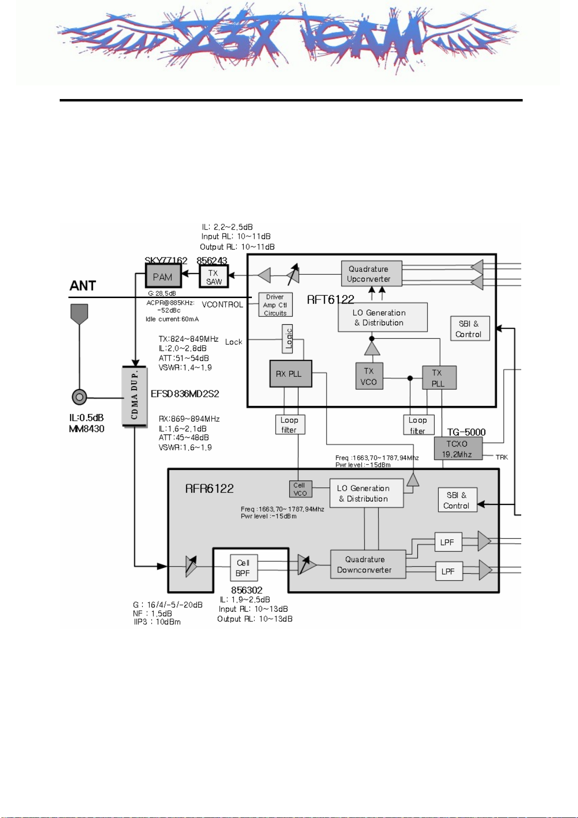
2.Circuit Description
power amp.After that, the RF signal is amplified by the Power Amp in order to
have enough power for radiation.
Finally, the RF signal is sent out to the cell site via the antenna after going through
the duplexer.
Z3X-BOX.COM
[Figure 2-1] RF Block Diagram Of MD120
9

2.Circuit Description
2.2 Description of Receive Part Circuit
2.2.1 Duplexer (DP100)
The duplexer consists of the receive part bandpass filter (BPF) and the transmit part
bandpass filter (BPF) which have the function of separating transmit/receive signals
in the full duplex system using the transmit/receive common antenna. The transmit
part BPF is used to suppress noises and spurious waves entering the receive band
among transmit signals in order to prevent the drop in receive sensitivity
characteristics. The receive part BPF blocks the signals sent out from entering the
receive end in order to improve sensitivity characteristics.
Insertion loss (IL) in the transmit band is 2.8dB (Max), whereas IL in the receive
band is 2.1dB (Max). The receive band attenuation amount of transmit filter is
51dB (Min) and the transmit band attenuation amount of receive filter is 45dB or
more (Min).
2.2.2 LNA (U103)
The RFR6122 has cellular LNA. The characteristics of Low Noise Amplifier (LNA)
are low noise figure, high gain, high intercept point and high reverse isolation. The
frequency selectivity characteristic of mobile phone is mostly determined by LNA.
The specifications of MD120 LNA are described below
Parameter Gain Mode 0(G0) Gain Mode 1(G1) Gain Mode 2(G2) Gain Mode 3(G3 Unit
Gain
Noise Figure
Input IP3
2.2.3 Rx RF SAW FILTER (F101)
16 4 -5 -20 dB
1.5 5 5.5 20 dB
10 7 15 15 dBm
Z3X-BOX.COM
The main function of Rx RF SAW filter is to attenuate mobile phone spurious
10

2.Circuit Description
frequency, attenuate noise amplified by the LNA and suppress second harmonic
originating in the LNA.
2.2.4 Down-Converter Mixers (U103)
The RFR6122 device performs signal direct-down-conversion for Cellular
applications. It contains all the circuitry (with the exception of external filters)
needed to support conversion of received RF signals to baseband signals. The LO
Buffer Amplifier buffers the RF VCO to the RF Transmit Upconverter. RFR6122
offers the most advanced and integrated CDMA Rx solution designed to meet
cascaded Noise Figure (NF) and Third-order Intercept Point (IIP3) requirements of
IS-98C and J-STD-018 specifications for Sensitivity, Two-Tone Intermodulation,
and Single-tone Desense. Operation modes and band selection are specially
controlled from the Mobile Station Modem MSM6000.
The specification of MD120 Mixers are described below:
Parameter High Gain Mode Low Gain Mode Unit
Noise Figure
Input IP3
Input IP2
10 25 dB
4 0 dBm
56 30 dBm
Z3X-BOX.COM
2.3 Description of Transmit Part Circuit
2.3.1 Description on the Internal Circuit of MSM6000 (U201) and RFT6122 (U102)
For the transmit data path(Tx), the MSM6000 modulates, interpolates, and converts
the digital signal into an analog baseband before sending it to the RFT6122. The
RFT6122 upconverts the Tx analog baseband into RF. The MSM6000
communicates with the external RF and analog baseband to control signal gain in
the RF Rx and Tx signal paths, educe base band offset errors, and tune the system
11

2.Circuit Description
frequency reference. The RFT6122 baseband-to-RF Transmit Processor performs
all Tx signal-processing functions required between digital baseband and the Power
Amplifier Module (PAM). The baseband quadrature signals are upconverted to the
Cellular frequency bands and amplified to provide signal drive capability to the
PAM. The RFT6122 includes an mixer for up-converting analog baseband to RF, a
programmable PLL for generating Tx and Rx LO frequency, cellular driver
amplifier and Tx power control through an 85 dB VGA. As added benefit, the
single sideband upconversion eliminates the need for a band-pass filter normally
required between the upconverter and driver amplifier. I, I/, Q and Q/ signals
proceed from the MSM6000 to RFT6122 are analog signal. In CDMA mode,
These signals are modulated by Offset Quadrature Phase Shift King (OQPSK). I
and Q are 90 deg. out of phase, and I and I/ are 180 deg. The mixer in RFT6122
converts baseband signals into RF signals. After passing through the upconverters,
RF signal is inputted into the Power Amplifier Module.
The RFT6122 Cellular CDMA RF specifications are described below:
Rated Output Power
Min Output Power
Rx band noise power
ACPR
2.3.2 Power Amplifier (U104)
Z3X-BOX.COM
Condition Min. Typ. Max. Unit
Average CDMA Cellular 6 dBm
Average CDMA Cellular -75 dBm
CDMA Cellular -132 dBm/Hz
Cellular: Fc±885kHz
Fc±1.98MHz
-52
-63
dBc
dBc
The power amplifier that can be used in the CDMA mode has linear amplification
capability. For higher efficiency, it is made up of one module (Monolithic
12

2.Circuit Description
Microwave Integrated Circuit) for which RF input terminal and internal interface
circuit are integrated onto one IC after going through the GaAs HBT(heterojunction
bipolar transistor) process.
The module of power amplifier is made up of an output end interface circuit
including this module. The maximum power that can be inputted through the input
terminal is +7dBm and conversion gain is about 28.5dB. RF transmit signals that
have been amplified through the power amplifier are sent to the duplexer.
2.4 Description of Frequency Synthesizer Circuit
2.4.1 Voltage Controlled Temperature Compensation Crystal Oscillator (X100)
The temperature range that can be compensated by VC-TCXO which is the
reference frequency generator of a mobile station is -30~+80 °C.
VC-TCXO receives frequency tuning signals called TRK_LO_ADJ from
MSM6000 as 0.5V~2.5V DC via R and C filters in order to generate the reference
frequency of 19.20MHz and input it into the frequency synthesizer of UHF band.
Frequency stability depending on temperature is ±2.0 ppm.
2.4.2 Voltage Controlled Oscillator (U103)
The internal VCO signal of RFR6122 is processed by the LO generation and
Z3X-BOX.COM
distribution circuits in RFR6122 to create Cellular quadrature downconverter’s LO
signals. The LO signals applied at the mixer ports are at the frequency different
than the VCO frequency. This assures that the VCO frequency is different than the
RF frequency, an important consideration for Zero-IF processing. The VCO
frequency used are 1738.08~1787.94MHz for cellular and It is produced in single
13

2.Circuit Description
voltage controlled oscillator of U106.
2.5. Digital/Voice Processing Part
2.5.1 Overview
The digital/voice processing part processes the user's commands and processes all
the digital and voice signal processing in order to operate in the phone. The
digital/voice processing part is made up of a keypad/LCD, receptacle part, voice
processing part, mobile station modem part, memory part, and power supply part.
2.6 Configuration
2.6.1 Keypad/LCD and Receptacle Part
This is used to transmit keypad signals to MSM6000. It is made up of a keypad
backlight part that illuminates the keypad, LCD part that displays the operation
status on to the screen, and a receptacle that receives and sends out voice and data
with external sources.
2.6.2 Voice Processing Part
The voice processing part is made up of an audio codec in MSM6000 used to
convert MIC signals into digital voice signals and digital voice signals into analog
voice signals, amplifying parts for amplifying the voice signals and MIC signals are
Z3X-BOX.COM
on Codec in MSM6000.
2.6.3 MSM6000 (Mobile Station Modem) Part
MSM6000 is the core elements of a CDMA mobile station and carries out the
functions of CPU, encoder, interleaver, deinterleaver, Viterbi decoder, Mod/Demod,
codec, and vocoder.
2.6.4 Memory Part
The memory part is made up of a flash memory and a SRAM
14

2.Circuit Description
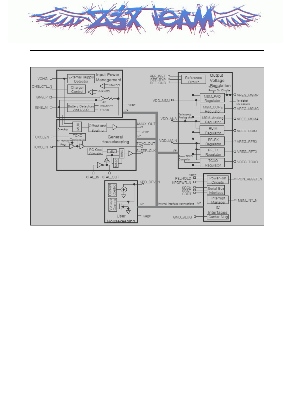
2.6.5 Power Supply Part
The PMIC(PM6610-2) is made up of 7 Regulators and direct connet to Batt.
Regulator(150mA)s give the power each Circuits(RFT6122/RFR6122).
Regulator(150mA) gives the power to the MSM and memory parts. PAM, Motor,
LCD back light LED, Indicator LED, Keypad LED and Audio amplifier are directly
conneted to Battery.
2.7 Briefly Circuit Description
2.7.1 Keypad/LCD and Receptacle Part
Once the keypad is pressed, the key signals are sent out to MSM6000 for
processing. In addition, when the key is pressed, the keypad lights up through the
use of 10 LEDs. The status and operation of a mobile station are displayed on the
screen for the user with the characters and icons on the LCD
Receptacle(CON400) exchanges audio signals and data with external sources and
then, receives power from the battery or external batteries.
2.7.2 MSM Part
MSM6000 is the core element of a CDMA mobile station. Subsystems within the
MSM6000 include a CDMA processor, an EVRC(Enhanced Variable Rate Codec)
.
Z3X-BOX.COM
vocoder, an ARM7TDMI microprocessor ,and assorted peripheral interfaces that
are used to support other functions. MSM6000, when operated in the CDMA mode,
utilizes CHIP×8 (9.8304MHz) as the reference clock primarily for CDMA and
vocoder processing.MSM6000 also uses TCXO/4 (4.92MHz). The CPU controls
total operations of the subscriber unit. Digital voice data, that have been inputted,
are encoded using the EVRC algorithm. Then, they are convolutionally encoded so
15

2.Circuit Description
that error detection and correction are possible. Coded symbols are interleaved in
order to avoid a burst error. Each data channel is scrambled by the long code PN
sequence of the user in order to ensure the confidentiality of calls.
Moreover, binary quadrature codes are used based on Walsh functions in order to
discern each channel. Data created thus are 4-phase modulated by one pair of Pilot
PN code and they are used to create I and Q data.
When received, I and Q data are demodulated into symbols by the demodulator and
then, de-interleaved in reverse to the case of transmission. Then, the errors of data
received from Viterbi decoder are detected and corrected. They are voice decoded
at the vocoder in order to output digital voice data.
The MSM6000 also supports Enhanced Variable Rate Coder (EVRC) operation in
addition to the standard 8k.
2.7.3 Audio Processing Part
MIC signals are inputted into the audio codec, and amplified with programmable
gain, and converted into digital signals(PCM). Then, they are inputted into
MSM6000. In addition, digital audio signals(PCM) outputted from MSM6000 are
Z3X-BOX.COM
converted into analog signals after going through the audio codec. These signals are
amplified with programmable gain on codec’s internal AMP and external Audio
AMP and then transferred to the ear piece. The signals is generated in MSM6000
using SW MIDI.
2.7.4 Memory Part
The memory part consists of a 32Mbits Flash Memory and a 16Mbits SRAM. In the
16

2.Circuit Description
Flash Memory, there are programs used for the operation of a mobile station. The
programs can be changed through down loading after the assembling of mobile
stations. The Flash memory is also emulated as an EEPROM to store
ESN(Electronic Serial Number), Calibration Data, etc. On the SRAM, data
generated during the operation of a mobile station are stored temporarily.
2.8 Power Supply Part
Turn ON
When the battery voltage (4.2V ~ 3.3V) is fed and the PWR key of keypad is
pressed, PMIC is activated by the ON_SW signal, and then the control signal
ON_SW_S/ signal is generated. And then, the regurator 2.4V_MSMC &
2.8V_MSMP, 2.6V_MSMA, are operated.
Operating
During the phone is on operating state, LDO(in PMIC) for MSM is always enable
and gives the power MSM6000 and memory part LDO(in PMIC) for +2.6V_TX
part is enabled on IDLE/ state, and gives the power TX part devices. LDO(in PMIC)
for +2.6V_RX part is enabled on SLEEP/ state, and gives the power RX part
devices
Turn OFF
When the PWR key is pressed during a few seconds, PMIC is turned on by ON_SW
and then, 'Low' is outputted on ON_SW_S/. MSM6000 receives this signal and then,
recognizes that the POWER key has been pressed. During this time, MSM6000
17
.
Z3X-BOX.COM
2.Circuit Description
outputs PS_HOLD as low and turn off all devices
[Figure 1-2] Block Diagram Of Power Management IC
2.9 Logic Part
The Logic part consists of internal CPU of MSM6000, MEMORY. The MSM6000
receives TCXO/4 clock(19.20Mz) and CHIPX8 clock signals, and then controls the
Z3X-BOX.COM
phone during the CDMA and the FM mode. The major components are as follows:
CPU : ARM7TDMI microprocessor core
MEMORY : S71PL064JB06AWOUO
CPU
ARM7TDMI 32-bit microprocessor is used and CPU controls all the circuitry.
Some of the features of the ARM microprocessor include a 3 stage pipelined RISC
18

2.Circuit Description
architecture, both 32-bit ARM and 16bit THUMB instruction setsm, a 32-bit
address bus, and a 32-bit internal data bus.
MEMORY
ARCHITECTURAL ADVANTAGES
■64 Mbit Page Mode devices
—Page size of 8 words: Fast page read access from random locations within the page
■Single power supply operation
—Full Voltage range: 2.7 to 3.6 volt read, erase, and program operations for battery-powered applications
■Simultaneous Read/Write Operation
—Data can be continuously read from one bank while executing erase/program functions in another bank
—Zero latency switching from write to read operations
FlexBank Architecture (PL064J)
—4 separate banks, with up to two simultaneous operations per device
—Bank A: PL064J - 8 Mbit (4 Kw x 8 and 32 Kw x 15)
—Bank B: PL064J - 24 Mbit (32 Kw x 48)
—Bank C: PL064J - 24 Mbit (32 Kw x 48)
—Bank D: PL064J - 8 Mbit (4 Kw x 8 and 32 Kw x 15)
Enhanced VersatileI/OTM (VIO) Control
—Output voltage generated and input voltages tolerated on all control inputs and I/Os is determined by
the voltage on the VIO pin
—VIO options at 1.8 V and 3 V I/O for PL127J devices
—3V VIO for PL064J and PL032J devices
SecSiTM (Secured Silicon) Sector region
—Up to 128 words accessible through a command sequence
—Up to 64 factory-locked words
—Up to 64 customer-lockable words
Both top and bottom boot blocks in one device
■Manufactured on 110 nm process technology
■Data Retention: 20 years typical
■Cycling Endurance: 1 million cycles per sector typical
Z3X-BOX.COM
PERFORMANCE CHARACTERISTICS
■High Performance
—Page access times as fast as 20 ns
—Random access times as fast as 55 ns
19

2.Circuit Description
■Power consumption (typical values at 10 MHz)
—45 mA active read current
—17 mA program/erase current
—0.2 µA typical standby mode current
KEYPAD
For key recognition, key matrix is setup using KEY_SENSE0-4_N signals and
GPIO32~36 of output ports of MSM6000. Backlight circuitry are included in the
keypad for easy operation in the dark.
LCD MODULE
LCD module contains a controller which will display the information onto the LCD
by 8-bit data from the MSM.
Z3X-BOX.COM
20
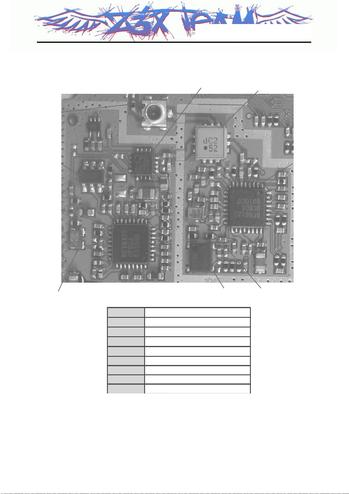
U100
U101
U102
F100
3.1 RF Component
Figure 1
U100 Mobile Switch
U100 Mobile Switch
U101 LOAD-SWITCH
U101 LOAD-SWITCH
U102 RF-TRANSMITTER
U102 RF-TRANSMITTER
Z3X-BOX.COM
U103 RF-RECEIVER
U103 RF-RECEIVER
U104 PAM
U104 PAM
F100 SAW-FILTER
F100 SAW-FILTER
F101 SAW-FILTER
F101 SAW-FILTER
X100 VCTCXO
X100 VCTCXO
DP100 DCN-DUPLEXER
DP100 DCN-DUPLEXER
3.TROUBLE SHOOTING
U104
X100
DP100
F101
U103
21

3.TROUBLE SHOOTING
3.2 RX Trouble
CHECKING FLOW
Z3X-BOX.COM
START
Set RX test(HHP)
。test mode -d
。CH“400”
Set E5515C
。CH:400
。CELL POWER:-30dBm
Spectrum Analyzer Setting
Oscilloscope Setting
(1) Check
PMIC circuit
(2) Check
VCTCXO
(3) Check
Mobile SW
&FEM
(4) Check
RX IQ
Redownload SW or
Do calibration again
22
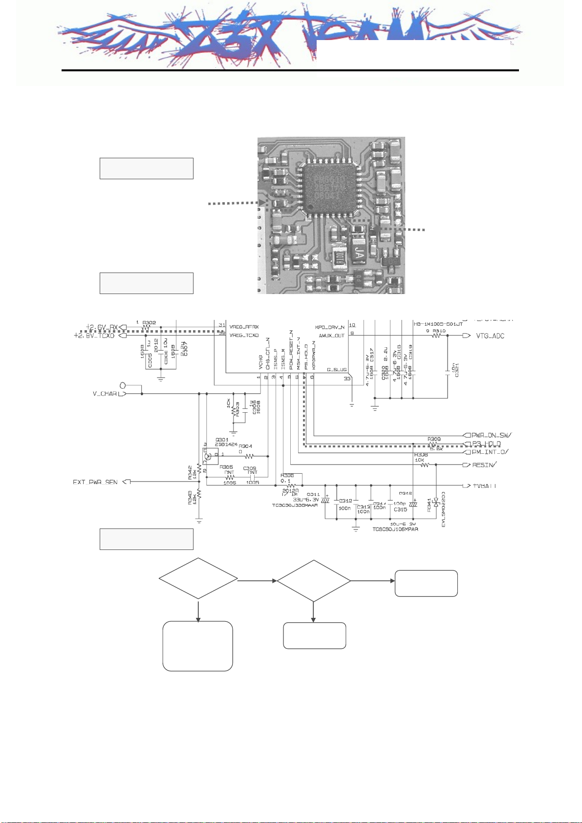
(1) Checking PMIC Circuit
CIRTUIT DIAGRAM
Check pin 31 o
f U300
TEST POINT
U300,PIN31
(+2.6V_RX)
Checking Flow
3.TROUBLE SHOOTING
U300,PIN7
(PS_HOLD)
Check pin 7
of U300
Z3X-BOX.COM
+2.6V_RX
OK?
Yes
PMIC is ok,,see t
he next page
to check the
VCTCXO
NO
PS_HOLD
is high?
Yes
Replace U300
NO
Changing the
board
23
 Loading...