

LG MBS-K62V, MBD-K62Q Schematic

MINI HOME THEATER SYSTEM
SERVICE MANUAL
MODELS: MBD-K62Q, MBS-K62V
CAUTION
BEFORE SERVICING THE UNIT, READ THE “SAFETY PRECAUTIONS”
IN THIS MANUAL.
MODELS: MBD-K62Q, MBS-K62V
SERVICE MANUAL
P/NO : AFN33894946 MAY, 2007
http://biz.lgservice.com

CONTENTS
SECTION 1
SUMMARY
SERVICING PRECAUTIONS ......................................1-2
• NOTES REGARDING HANDLING OF THE PICK-UP
•
NOTES REGARDING COMPACT DISC PLAYER REPAIRS
ESD PRECAUTIONS ...................................................1-4
SPECIFICATIONS ........................................................1-5
SECTION 2
EXPLODED VIEWS
1. CABINET AND MAIN FRAME SECTION..............2-1
2. DECK MECHANISM SECTION (DP-10A).............2-3
3. SPEAKER SECTION (MBS-K62V) ........................2-5
4. PACKING ACCESSORY SECTION .......................2-6
SECTION 3
ELECTRICAL
ELECTRICAL TROUBLESHOOTING
GUIDE OF AUDIO PART.............................................3-1
1. MICOM PART CHECK I ....................................3-1
2. MICOM PART CHECK II ...................................3-2
3. IC103 KS4CD21CS CHECK.............................3-3
4. FLD DISPLAY CHECK ......................................3-4
5. PWM MODULATION PART ..............................3-5
6. POWER AMP PART CHECK............................3-6
7. PORTABLE FUNCTION ....................................3-7
8. TV-AUDIO FUNCTION ......................................3-8
9. TUNER FUNCTION CHECK ............................3-9
10. SMPS POWER TROUBLESHOOTING.........3-10
11. BLUETOOH PART (OPTIONAL PART)..........3-13
12. IPOD PART (OPTIONAL PART) .....................3-14
ELECTRICAL TROUBLESHOOTING
GUIDE OF DVD PART...............................................3-15
1. POWER CHECK GUIDE.................................3-15
2. TEST & DEBUG FLOW...................................3-16
3. USB PART ........................................................3-21
WAVEFORMS.............................................................3-22
1. WHEN POWER ON, RESET & DATA
ETC WAVEFORM ............................................3-22
2. OPEN / CLOSE WAVEFORM AT
POWER ON......................................................3-23
3. STARTING ACTION WAVEFORM
IN MD DEVICE ................................................3-23
4. FOCUS WAVEFORM ......................................3-24
5. AT POWER ON, SPINDLE SIGNAL AT
MD DECK .........................................................3-25
6. AT FIRST ACTION, FOCUS
SIGNAL A, B, C, D............................................3-25
7. TRACKING SIGNAL ........................................3-26
8. RF WAVEFORM ..............................................3-26
9. DISK TYPE JUGEMENT WAVEFORM..........3-27
INTERNAL BLOCK DIAGRAM OF ICs...................3-28
1. AK5358..............................................................3-28
2. EM639165 ........................................................3-30
3. ES29LV160E ....................................................3-32
4. HT1000 .............................................................3-34
5. IP9009...............................................................3-37
6. KS24L161 .........................................................3-38
7. MC4580 ............................................................3-39
8. PS9829B...........................................................3-40
9. PT6324..............................................................3-41
10. STR-A6252 .......................................................3-44
11. µPD78F0546R (R)............................................3-45
WIRING DIAGRAM ....................................................3-49
BLOCK DIAGRAMS ..................................................3-51
1. SMPS BLOCK DIAGRAM...............................3-51
2. MAIN & FRONT BLOCK DIAGRAM ..............3-53
SCHEMATIC DIAGRAMS .........................................3-55
1. SMPS SCHEMATIC DIAGRAM......................3-55
2. MAIN, INTERFACE & PWM
SCHEMATIC DIAGRAM..................................3-57
3. MPEG SCHEMATIC DIAGRAM .....................3-59
4. SERVO SCHEMATIC DIAGRAM ...................3-61
5. INTERFACE SCHEMATIC DIAGRAM ...........3-63
6. FRONT SCHEMATIC DIAGRAM ..................3-65
7. FRONT MIC SCHEMATIC DIAGRAM ...........3-67
8.
IPOD-1 SCHEMATIC DIAGRAM (OPTION)
9.
IPOD-2 SCHEMATIC DIAGRAM (OPTION)
2 CHANNEL AMP SCHEMATIC DIAGRAM
10.
11. BLUTHOOTH MODULE
SCHEMATIC DIAGRAM (OPTION) ................3-75
CIRCUIT VOLTAGE CHART.....................................3-77
PRINTED CIRCUIT BOARD DIAGRAMS ...............3-79
1. MAIN P.C.BOARD............................................3-79
2. FRONT P.C.BOARD ........................................3-83
3. SMPS P.C.BOARD ..........................................3-85
4. MIC JACK P.C.BOARD ...................................3-87
5. IPOD P.C.BOARD (OPTION)..........................3-87
.....3-69
.....3-71
......3-73
SECTION 4
REPLACEMENT PARTS LIST
........4-1
1-1
SECTION 1 SUMMARY
SERVICING PRECAUTIONS
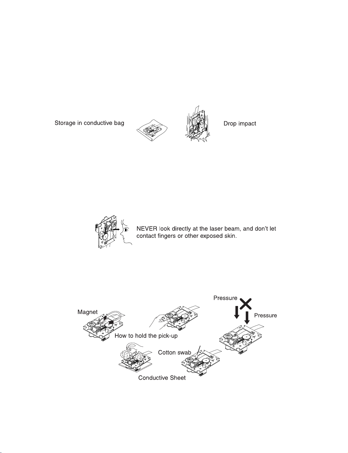
NOTES REGARDING HANDLING OF THE PICK-UP
1. Notes for transport and storage
1) The pick-up should always be left in its conductive bag until immediately prior to use.
2) The pick-up should never be subjected to external pressure or impact.
2. Repair notes
1) The pick-up incorporates a strong magnet, and so should never be brought close to magnetic materials.
2) The pick-up should always be handled correctly and carefully, taking care to avoid external pressure and
impact. If it is subjected to strong pressure or impact, the result may be an operational malfunction and/or
damage to the printed-circuit board.
3) Each and every pick-up is already individually adjusted to a high degree of precision, and for that reason
the adjustment point and installation screws should absolutely never be touched.
4) Laser beams may damage the eyes!
Absolutely never permit laser beams to enter the eyes!
Also NEVER switch ON the power to the laser output part (lens, etc.) of the pick-up if it is damaged.
5) Cleaning the lens surface
If there is dust on the lens surface, the dust should be cleaned away by using an air bush (such as used
for camera lens). The lens is held by a delicate spring. When cleaning the lens surface, therefore, a cotton
swab should be used, taking care not to distort this.
6) Never attempt to disassemble the pick-up.
Spring by excess pressure. If the lens is extremely dirty, apply isopropyl alcohol to the cotton swab. (Do not
use any other liquid cleaners, because they will damage the lens.) Take care not to use too much of this
alcohol on the swab, and do not allow the alcohol to get inside the pick-up.
1-2

NOTES REGARDING COMPACT DISC PLAYER REPAIRS
1. Preparations
1) Compact disc players incorporate a great many ICs as well as the pick-up (laser diode). These components
are sensitive to, and easily affected by, static electricity. If such static electricity is high voltage, components
can be damaged, and for that reason components should be handled with care.
2) The pick-up is composed of many optical components and other high-precision components. Care must be
taken, therefore, to avoid repair or storage where the temperature of humidity is high, where strong
magnetism is present, or where there is excessive dust.
2. Notes for repair
1) Before replacing a component part, first disconnect the power supply lead wire from the unit
2) All equipment, measuring instruments and tools must be grounded.
3) The workbench should be covered with a conductive sheet and grounded.
When removing the laser pick-up from its conductive bag, do not place the pick-up on the bag. (This is
because there is the possibility of damage by static electricity.)
4) To prevent AC leakage, the metal part of the soldering iron should be grounded.
5) Workers should be grounded by an armband (1MΩ)
6) Care should be taken not to permit the laser pick-up to come in contact with clothing, in order to prevent
static electricity changes in the clothing to escape from the armband.
7) The laser beam from the pick-up should NEVER be directly facing the eyes or bare skin.
1-3
ESD PRECAUTIONS
Electrostatically Sensitive Devices (ESD)
Some semiconductor (solid state) devices can be damaged easily by static electricity. Such components
commonly are called electrostatically sensitive devices (ESD). Examples of typical ESD devices are
integrated circuits and some field-effect transistors and semiconductor chip components. The following
techniques should be used to help reduce the incidence of component damage caused by static electricity.
1. Immediately before handling any semiconductor component or semiconductor-equipped assembly, drain
off any electrostatic charge on your body by touching a know earth ground. Alternatively, obtain and
wear a commercially available discharging wrist strap device, which should be removed for potential
shock reasons prior to applying power to the unit under test.
2. After removing an electrical assembly equipped with ESD devices, place the assembly on a conductive
surface such as aluminum foil, to prevent electrostatic charge buildup or exposure of the assembly.
3. Use only a grounded-tip soldering iron to solder or unsolder ESD devices.
4. Use only an anti-static solder removal device. Some solder removal devices not classified as "anti-static"
can generate electrical charges sufficient to damage ESD devices.
5. Do not use freon-propelled chemicals These can generate electrical charges sufficient to damage ESD
devices.
6. Do not remove a replacement ESD device from its protective package until immediately before you are
ready to install it. (Most replacement ESD devices are packaged with leads electrically shorted together
by conductive foam, aluminum foil or comparable conductive materials).
7. Immediately before removing the protective material from the leads of a replacement ESD device, touch
the protective material to the chassis or circuit assembly into which the device will by installed.
CAUTION : BE SURE NO POWER IS APPLIED TO THE CHASSIS OR CIRCUIT, AND OBSERVE ALL
OTHER SAFETY PRECAUTIONS.
8. Minimize bodily motions when handing unpackaged replacement ESD devices. (Otherwise harmless
motion such as the brushing together of your clothes fabric or the lifting of your foot from a carpeted floor
can generate static electricity sufficient to damage an ESD device).
[CAUTION. GRAPHIC SYMBOLS]
THE LIGHTNING FLASH WITH ARROWHEAD SYMBOL. WITHIN AN EQUILATERAL
TRIANGLE, IS INTENDED TO ALERT THE SERVICE PERSONNEL TO THE PRESENCE
OF UNINSULATED "DANGEROUS VOLTAGE" THAT MAY BE OF SUFFICIENT
MAGNITUDE TO CONSTITUTE A RISK OF ELECTRIC SHOCK.
THE EXCLAMATION POINT WITHIN AN EQUILATERAL TRIANGLE IS INTENED TO
ALERT THE SERVICE PERSONNEL TO THE PRESENCE OF IMPORTANT SAFETY
INFORMATION IN SERVICE LITERATURE.
1-4

SPECIFICATIONS
• GENERAL
Power supply Refer to the back panel of the unit.
Power consumption Refer to the back panel of the unit.
Net Weight 3.00kg
External dimensions (WxHxD) 300 x 130 x 243mm
• CD/DVD
Laser Semiconductor laser, wavelength 650nm
Signal system PAL 625/50, NTSC 525/60
Frequency response (audio) 40Hz to 20kHz
Signal-to-noise ratio (audio) More than 75dB (1kHz, NOP -3dB, 20kHz LPF/A-Filter)
Dynamic range (audio) More than 75dB
Harmonic distortion (audio) 0.5 % (1kHz, at 1W position) (20kHz LPF)
• VIDEO
Video output 1.0V (p-p), 75Ω, negative sync./ RCA jack x 1/ SCART (TO TV)
COMPONENT VIDEO OUT (Y) 1.0V (p-p), 75ohms, negative sync, RCA jack x 1
(Pb)/(Pr) 0.7V (p-p), 75ohms, RCA jack x 1
• TUNER
FM Tuning Range 87.5 ~ 108.0MHz or 65 ~ 74MHz, 87.5 ~ 108.0MHz
Intermediate Frequency 10.7MHz
Signal to Noise Ratio 60/55dB
Frequency Response 50 ~ 10000Hz
AM Tuning Range 522 ~ 1620kHz or 520 ~ 1720kHz
Intermediate Frequency 450kHz
Signal to Noise Ratio 30dB
Frequency Response 80 ~ 1800Hz
• AMPLIFIER
Output Power 30W + 30W
T.H.D 0.5%
Frequency Response 40 ~ 20000Hz
Signal-to-noise ratio 75dB
• SPEAKERS
Speaker Name MBS-K62V
Type Bass Reflex 2 Way 2 Speaker
Impedance 4Ω
Frequency Response 60 ~ 20000Hz
Sound Pressure Level 82dB/W (1m)
Rated Input Power 30W
Max. Input Power 60W
Net Dimensions (WxHxD) 160 X 308 X 204mm
Net Weight (1EA) 2.5kg
Designs and specifications are subject to change without notice.
1-5

MEMO
1-6
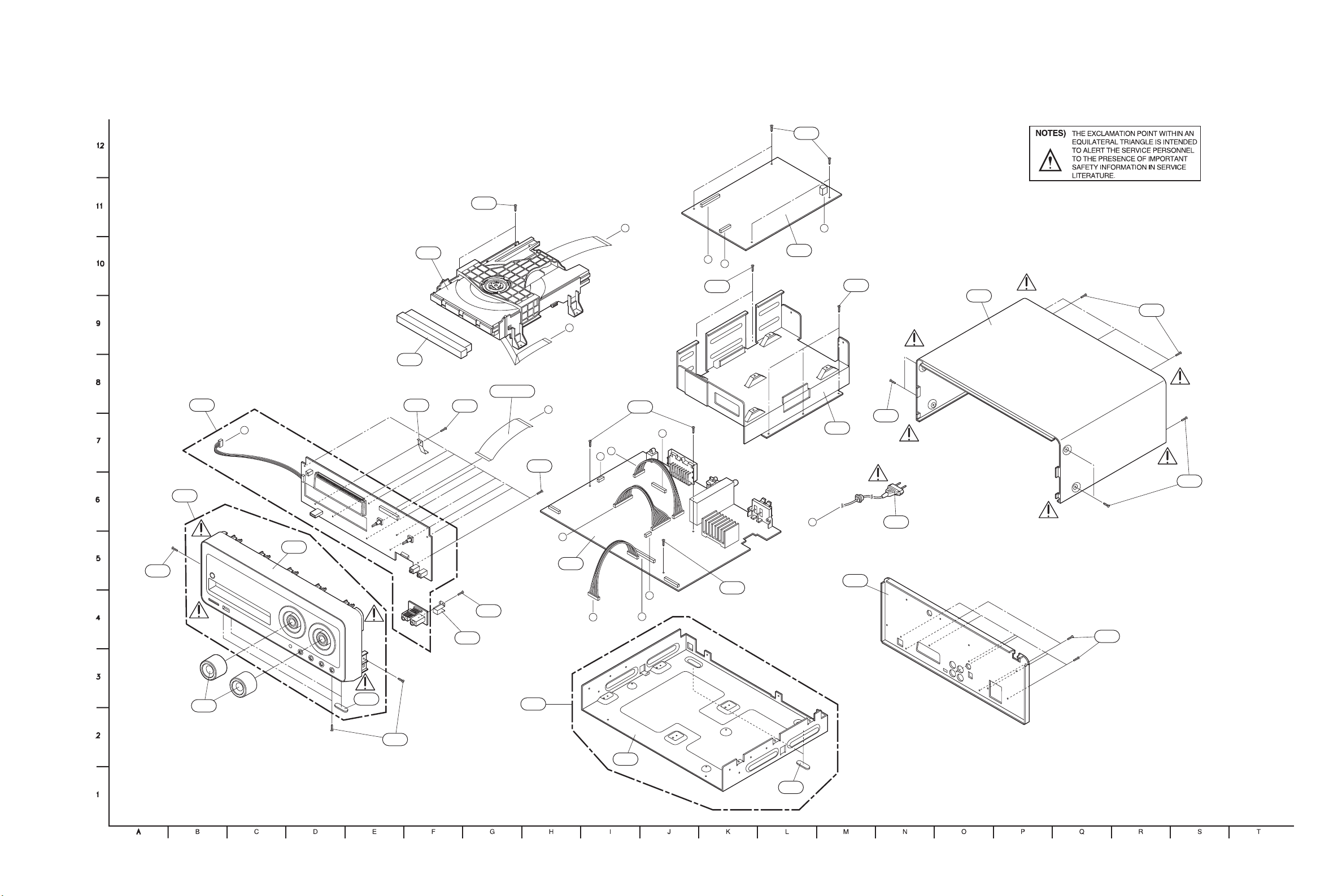
SECTION 2 EXPLODED VIEWS
1. CABINET AND MAIN FRAME SECTION
463
461
463
A43
A50
A26
A
C
D
461
E
A47
463
250
463
B
257
CABLE3
277
G
463
F
G
461
A
H
275
463
463
463
E
C
300
256
A46
276
463
B
D
F
461
258
259
463
272
463
A44
273
274
2-1 2-2
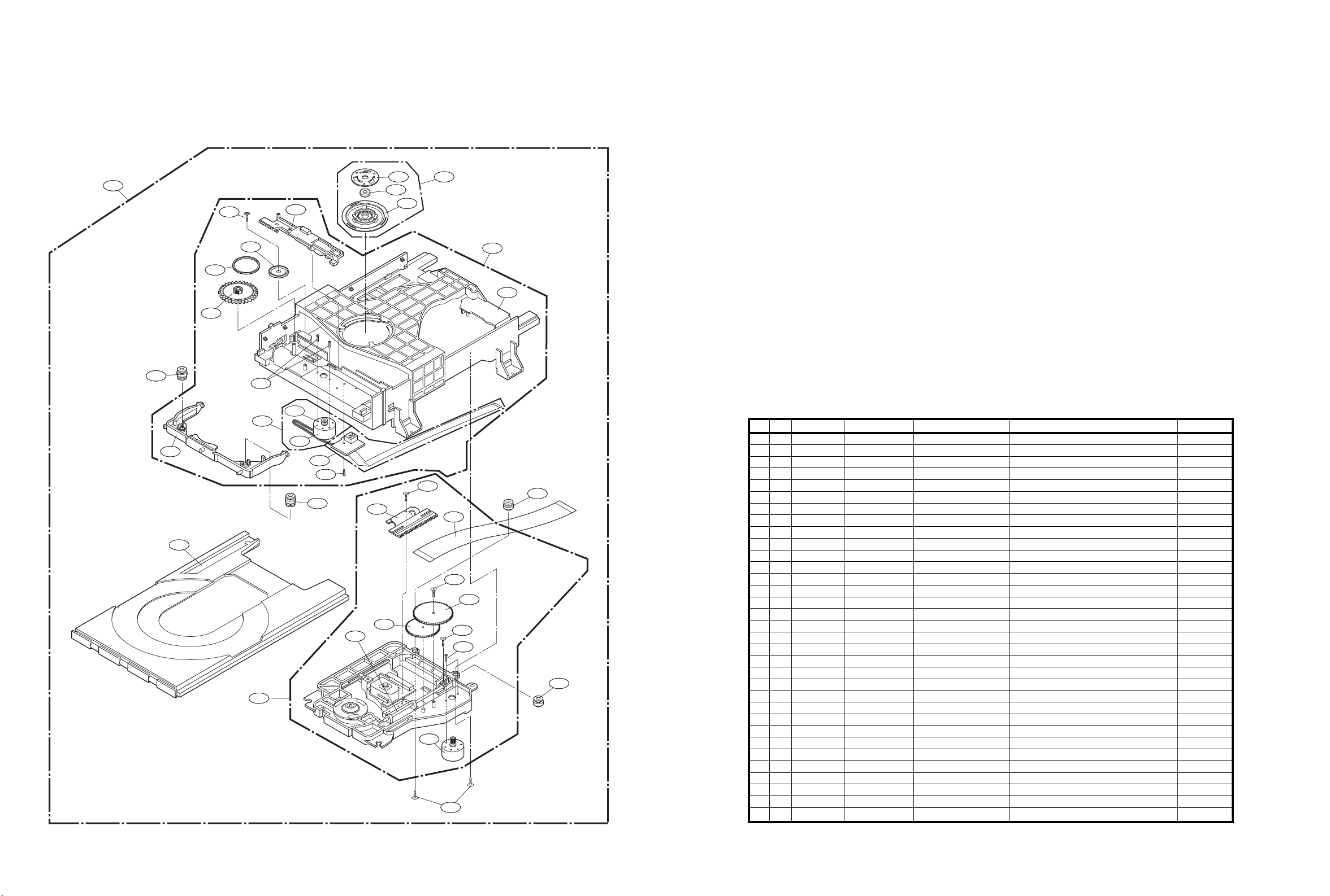
2. DECK MECHANISM SECTION (DP-10A)
A26
012
019
026
013
017
439
014
435
015
A03
018
015B
015A
016
012
440
036
030
025
001
002
003
432
021
A01
430
010
439
431
435
024
A02
020
012A
012A
NSP : Non SVC Parts
SALLOCA. NO. LG PART NO. DESCRIPTION SPECIFICATION REMARKS
A26 6721RJD100T Deck Assembly,DVD HOME THEATER DP-10A (HZ) NSP
A01 4861R-0016B Clamp Assembly DVD DISC DP7 - SH Clamp Assemb
A02 3041R-T010B Base Assembly DP-10A LOADING
A03 3041R-T011C Base Assembly SLED DP-10A (HZ)
001 3300R-0547A Plate PRESS SUS301 0.3 CDM-300 PRESS NSP
002 5016H-1016B Magnet CLAMP(LDM-R608,10*5,1*1.5T) NSP
003 4860R-0021A Clamp MOLD POM UPPER DP7 NSP
010 6850R-JW14B Cable,FFC 1.0 x 23 x 140 x B(0.035 x 0.6
012 5040R-0083A Damper PRINTING DVD DP-6, DP-8 FRONT
012A 5040R-0110A Damper PRINTING DVD REAR DP8 RIGHT 20
013 4400R-0006B Belt MOLD RUBBER DECK/MECHA DP2-5,
014 4470R-0154A Gear COMPLEX DVD DECK/MECHA DP8 PUL
015 4681R-A015A Motor,Unclassified DECK/MECHA LOADING DP-9 SH
015A 4680R-E008A Motor,DC RF-300EA-1D390(80MM) 2V 90MA 2 NSP
015A EAU36590901 Motor,DC FC08I20TLG-1 2V 100MA 0A 1.37K ALTERNATE
015B 4560R-0008A Pulley MOLD POM MOTOR
016 6871R-9297A PCB Assembly DP-10T LOADING/FEEDING
017 4470R-0176A Gear MOLD POM DVD DP-9 LOADING MO
018 4974R-0067A Guide MOLD POM DVD DP-9C UP/DOWN MOL
019 3210R-M008A Frame MOLD ABS DP-9C UP/DOWN MOLD
020 MAM32408101 Base MOLD ABS XR-401 MAIN MOLD DP-1
021 4681R-B009C Motor,Unclassified DECK/MECHA DP-10 FEEDING
024 4470R-0179A Gear MOLD POM DVD DP-9 PINION MOL
025 4470R-0178A Gear MOLD POM DVD DP-9 MIDDLE MOLD
026 3390R-0032A Tray MOLD ABS DVD DP-9MC DISK MOLD
030 4470R-0180A Gear MOLD POM DVD DP-9 RACK MOLD
036 4370R-0136A Shaft CUTTING STS 301 DVD PU, DR-02
430 1SZZR-0064B Screw,Customized - + 1.7MM 7MM SWRCH FZB SIN J
431 1SZZR-0062A Screw,Customized - + 1.7MM 4.5MM SWRCH NI PLT
432 1SZZR-0072A Screw,Customized - + 1.7MM 4.5MM SWRCH FZY SIN
435 1SZZR-0011A Screw,Customized MACHINE
439 1SZZR-0075A Screw,Customized - + 1.7MM 10MM SWRCH FZW SIN
440 1SZZH-1007B Screw,Customized + D2.0 6MM SWRCH16A/ZNBK 4MM 1
2-3 2-4
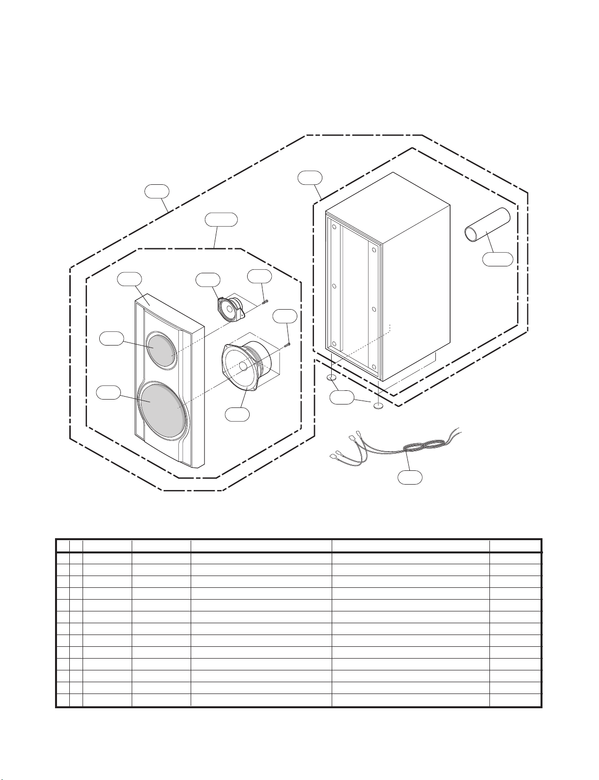
3. SPEAKER SECTION (MBS-K62V)
A70
A70A
757
757A
750
753
755
756
751
752
758
754
759
NSP : Non SVC Parts
SALLOCA. NO. LG PART NO. DESCRIPTION SPECIFICATION REMARKS
A70 EAB38086501 Speaker Assembly MBS62V 049-01368-07 SAMMI MBS6
A70A AGL33753501 Panel Assembly,Front SPK MBS62V BK 1coated spray NSP
750 MGC37897301 Panel,Front MOLD ABS SPK MBS102 MOLD BK GL NSP
751 MDX37897601 Grille PRESS EGI 0.4 MBS102 PRESS T/W NSP
752 MDX37897501 Grille PRESS EGI 0.6 MBS102 PRESS W/F NSP
753 EAB38121201 Speaker,Tweeter CTR-50B30L-1 FERRITE 30W 4OHM NSP
754 EAB38120701 Speaker,Woofer MCW-125B30L FERRITE 30W 4OHM 8 NSP
755 353M025F Screw,Customized - - 3MM 8MM - FZY SIN JIN BOL NSP
756 353M050M Screw,Customized - + 3.5MM 10MM MSWR FZY SIN J NSP
757 ACQ33753301 Cover Assembly SPK MBS62V CABINET ASSY, PB9T, NSP
757A 5208RM0056D Duct CUTTING PAPER SPK MBS102 OTHER NSP
758 3610RM0005A Foot CUTTING EVA HOME EVA EVA PHI 2 NSP
759 EBR36664806 PCB Assembly,Sub SAMMI MBS62 MBS62 NETWORK ASSY NSP
2-5
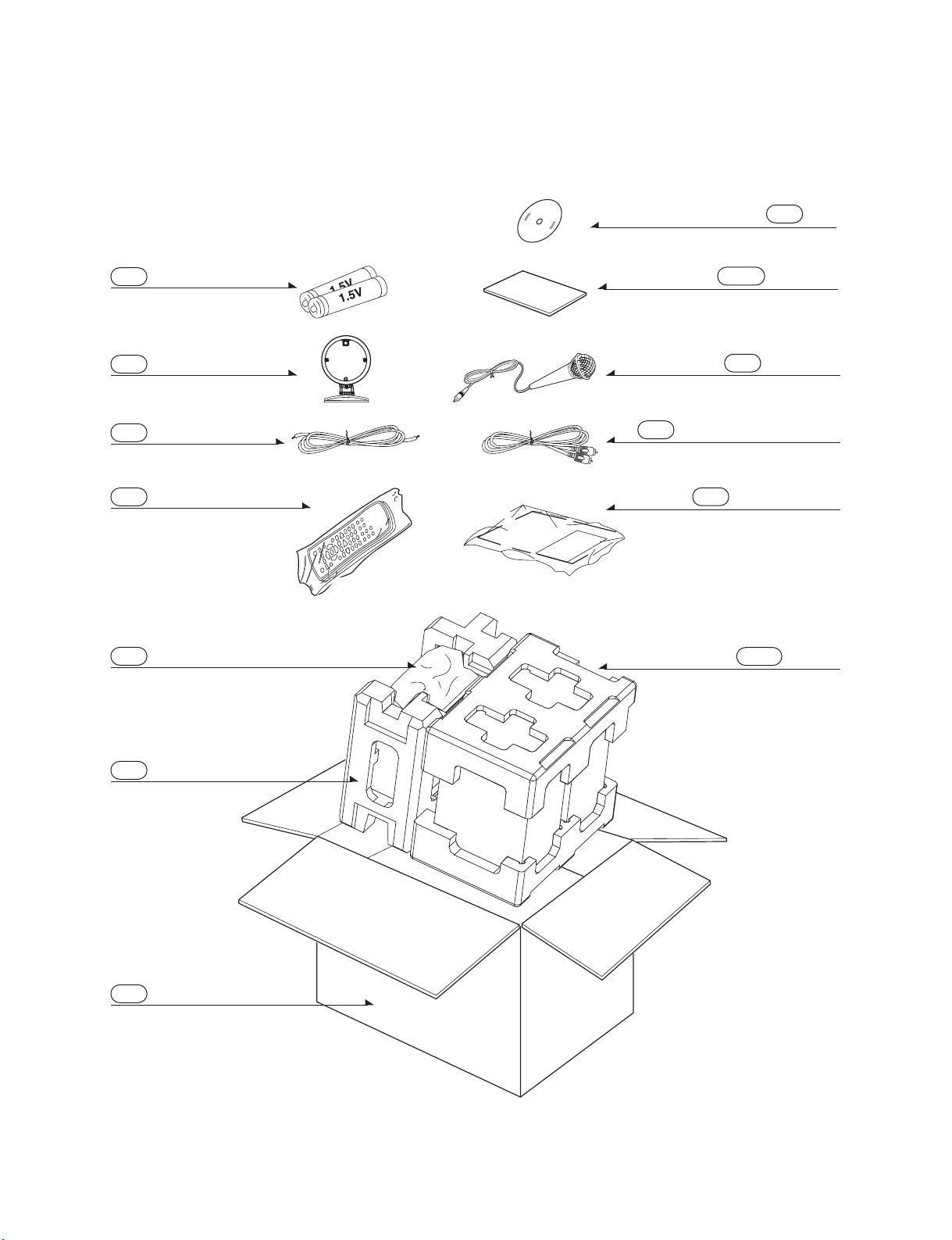
4. PACKING ACCESSORY SECTION
832
Disc
Battery
808
Antenna Loop
824
825
Antenna
900
Remote control
Bag804
827
Plug Ass'y, 1Way(BLACK)
811
Instruction Ass'y
801
803A
Song Book801S
Microphone
Packing
803
Packing
Box802
2-6

SECTION 3 ELECTRICAL
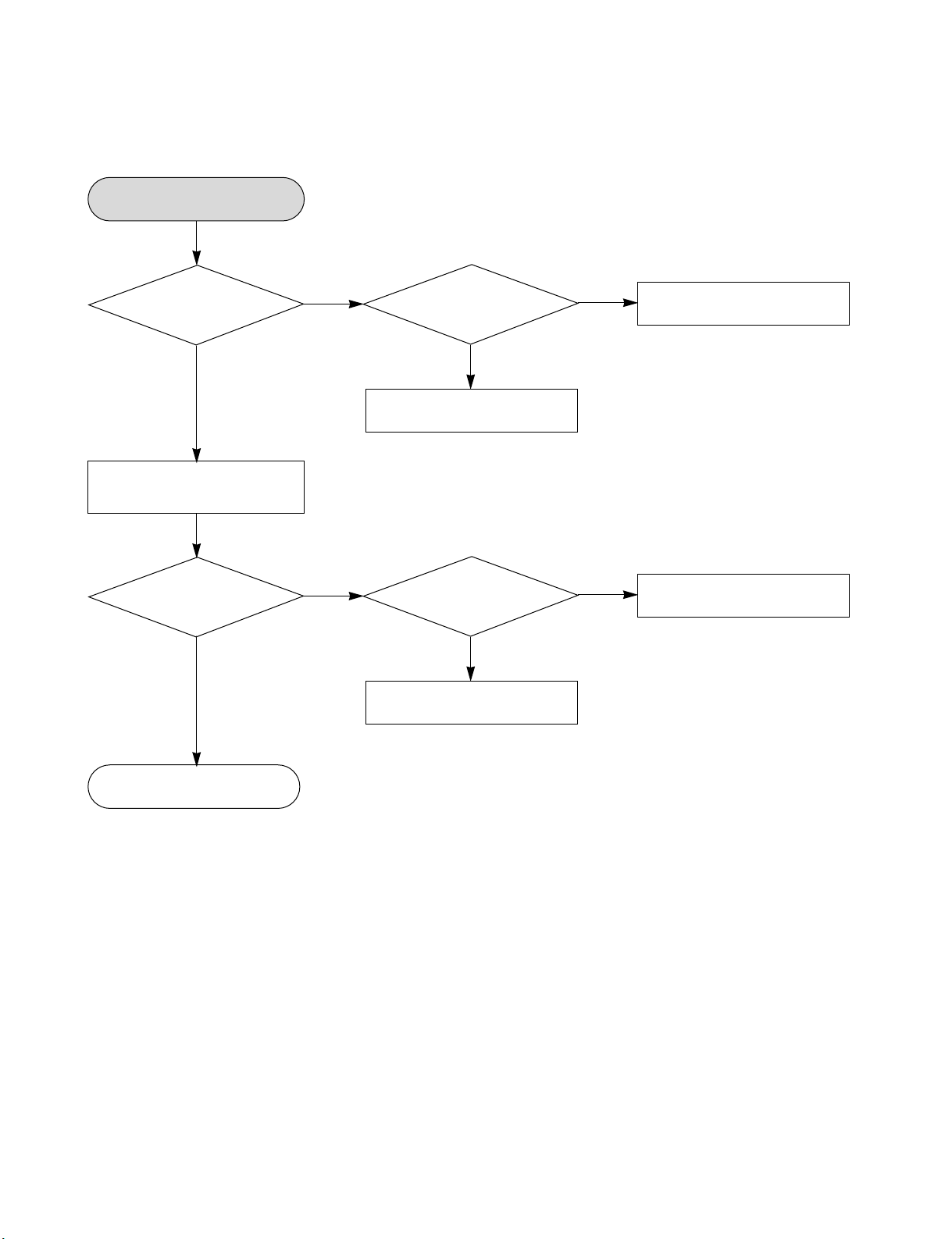
ELECTRICAL TROUBLESHOOTING GUIDE OF AUDIO PART
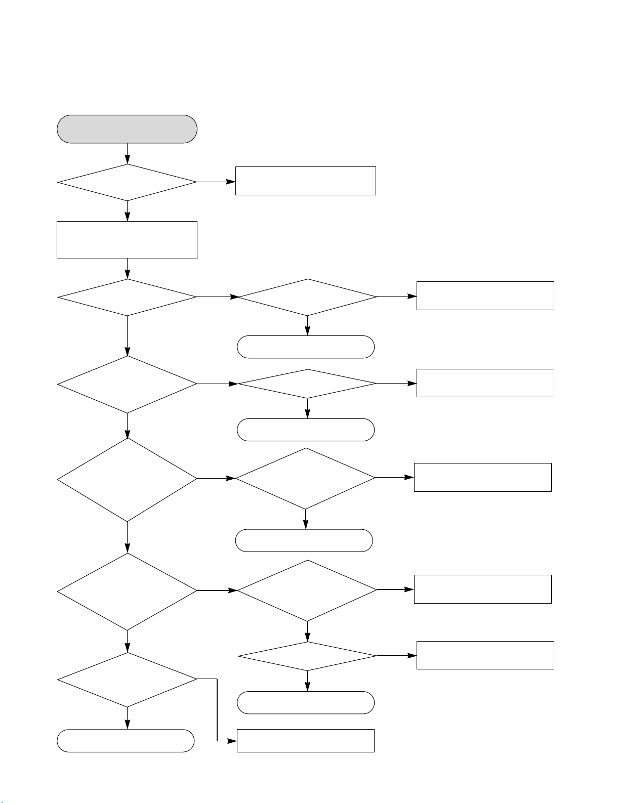
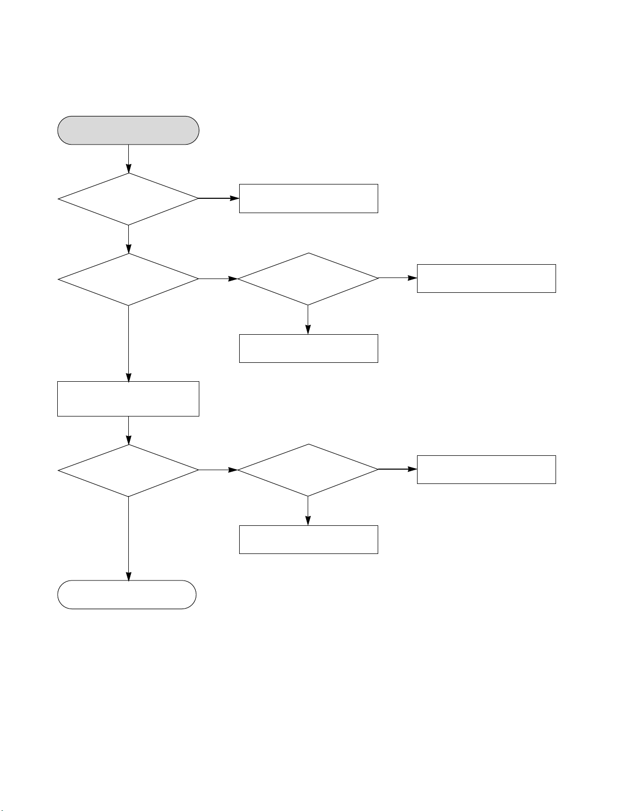
1. MICOM PART CHECK I
MICOM part check I
YES
Check P7904
6PIN P-SENS
YES
Check
power of both
terminals of IC101
KIA7042
YES
Check IC100 78KO/KF2
1PIN power
YES
OK OK
NO
NO
Refer to SMPS
Troubleshooting
Check
if IC101 KIA7042
input is over 5V.
YES
Check if output voltage
of IC101 KIA7042 is 4.3V
YES
NO
Check
the related part of
IC101 KIA7042
YES
NO
Replace the
related parts
3-1
ELECTRICAL TROUBLESHOOTING GUIDE OF AUDIO PART
2. MICOM PART CHECK II
MICOM part check II
YES
Check P7904
5PIN 5.6V
YES
Check power of
both terminals of D101
1SR35
YES
Check
Q101 EMITTER 5V
and COLLECTOR
5V
YES
Check IC103 8PIN IC100
19, 20, 59PIN 5V
NO
NO
NO NO
Refer to SMPS
Troubleshooting
Check D101 1SR35
output is working on 5V
YES
Check the
related part
YES
OK
Check Q102
BASE PIN 0.6V
HIGH
YES
Check Q102 COLLECTOR
NO
Replace the
related parts
Check output power
of IC101 KIA7042 is
over 4.3V.
YES
Check the
related part.
NO
Replace the
related parts
YES
Check the working condition
X101: 32.768kHz
X100: 9.8304MHz
YES
OK
YES
Check the
related part.
YES
OK
3-2
NO
YES
OK
Replace the
related parts
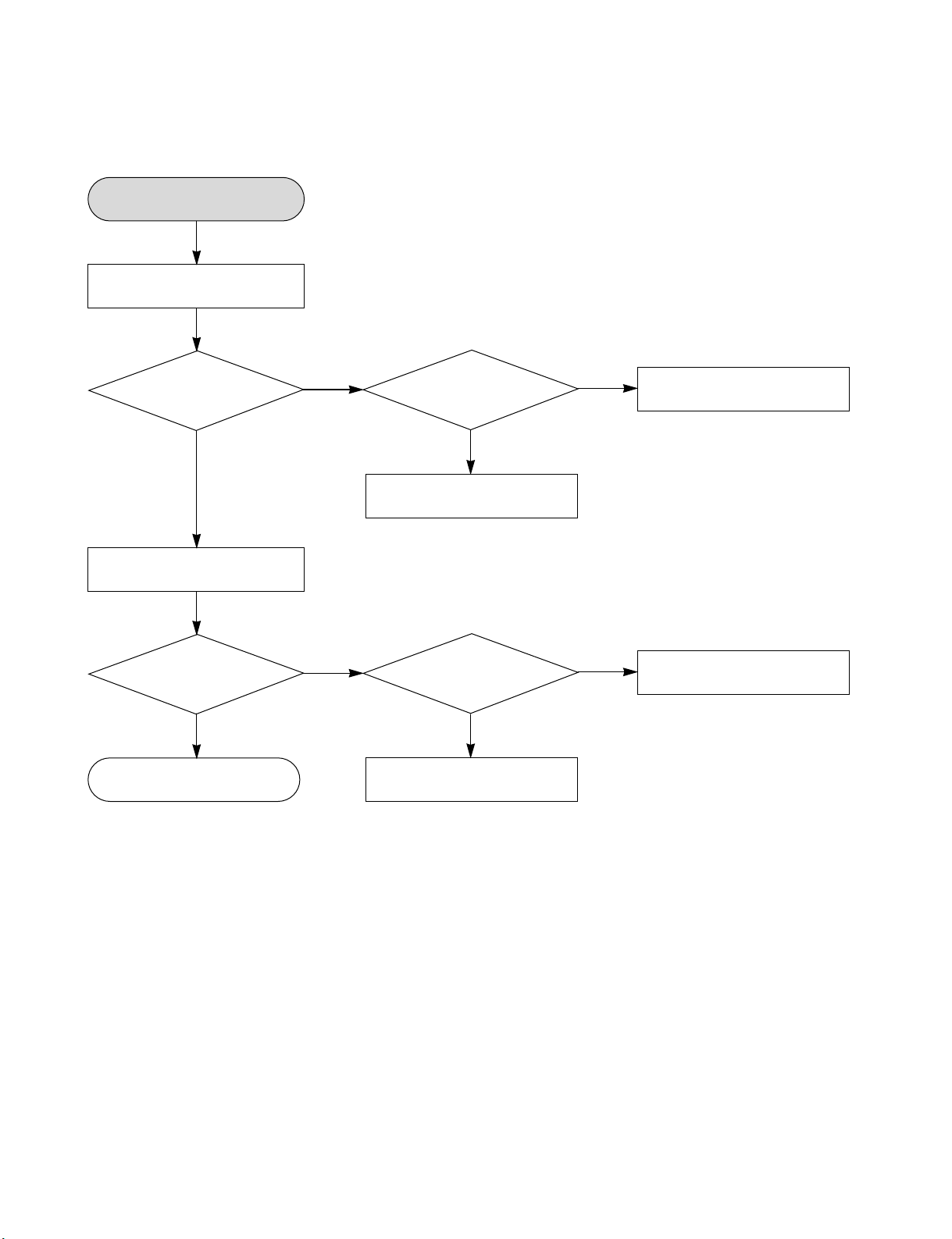
ELECTRICAL TROUBLESHOOTING GUIDE OF AUDIO PART
3. IC103 KS4CD21CS CHECK
Check IC100 78KOKF2
22, 24PIN
YES
22 PIN DATA
24 PIN CLK
YES
OK
Check MICOM
power 5V
YES
Check the
related part
YES
OK
NONO
NO
Refer to MICOM
Troubleshooting
Replace the related parts
3-3

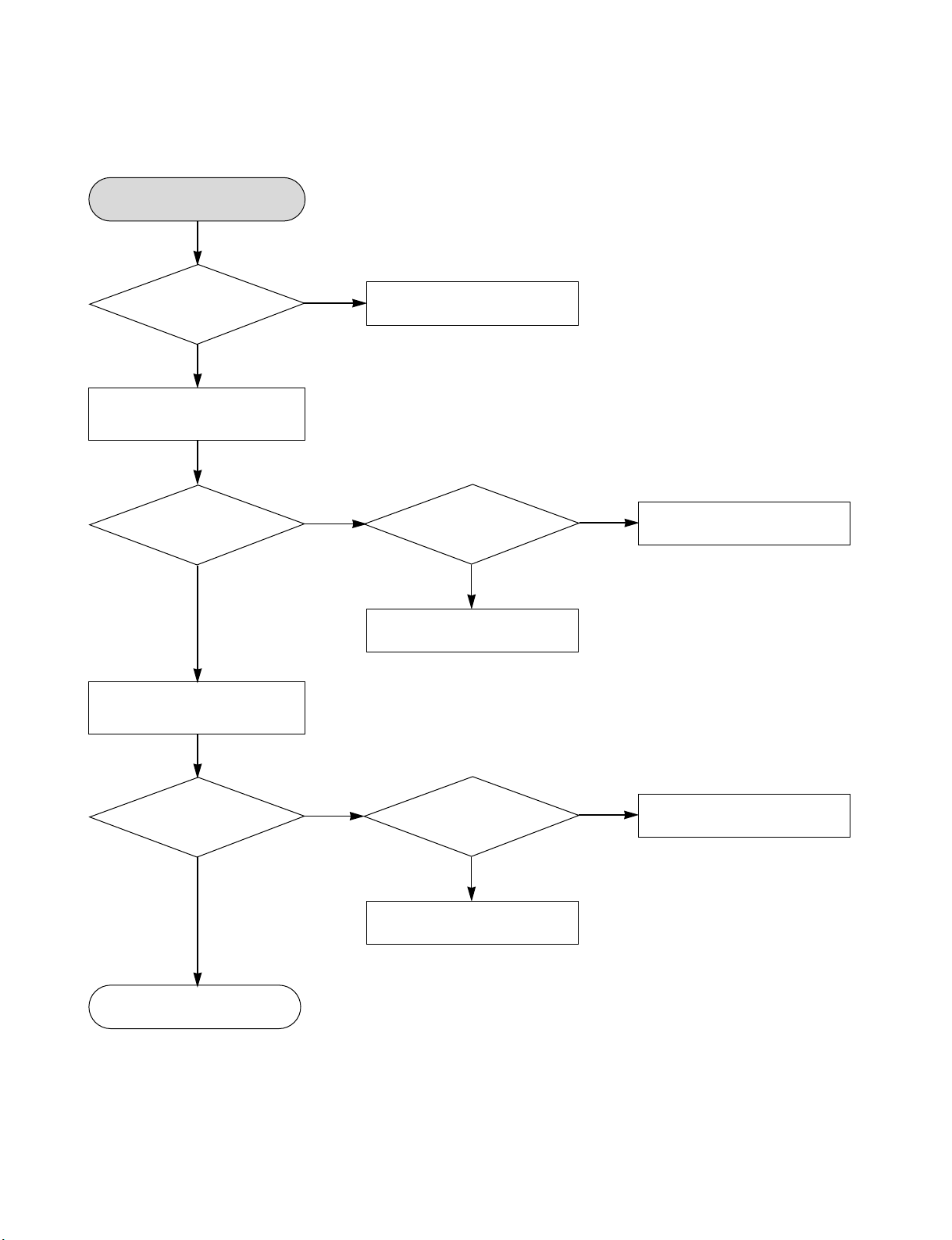
ELECTRICAL TROUBLESHOOTING GUIDE OF AUDIO PART
4. FLD DISPLAY CHECK
FLD display check
YES
Check P7904
1,2,3 power.
YES
F1+,F2- both
terminals: over 3.7V
Check power VKK: over -28V.
YES
Check
P7302 connection
condition and power F1+,
F2- both terminals: over 3.7V
Check power VKK: over
-28V Check 24
PIN:5.6V
YES
Check IC301
PT6324 power
50PIN VKK: -28V
9.51PIN +5V
NO
NO
NO
Refer to SMPS
Troubleshooting
Check P7302 assembly
YES
Check power
of each PIN
YES
OK
When 5V fails, check
D301SR35 input and
output power
YES
NO
Replace the related part
YES
Check IC100
--> IC301 DATA
communication
PIN PIN
75PIN-->3PIN STB
76PIN-->2PIN DO
78PIN-->1PIN
CLK
YES
YES
NO
Check the
related part
YES
OK
IC100
75PIN - > STB
78PIN - > 1PIN CLK
Check Data output.
YES
76PIN--> DO
--> DATA input
YES
Check the
related part
YES
OKOK
3-4
NO
NO
Replace the related part
Replace the related partFLD light on?
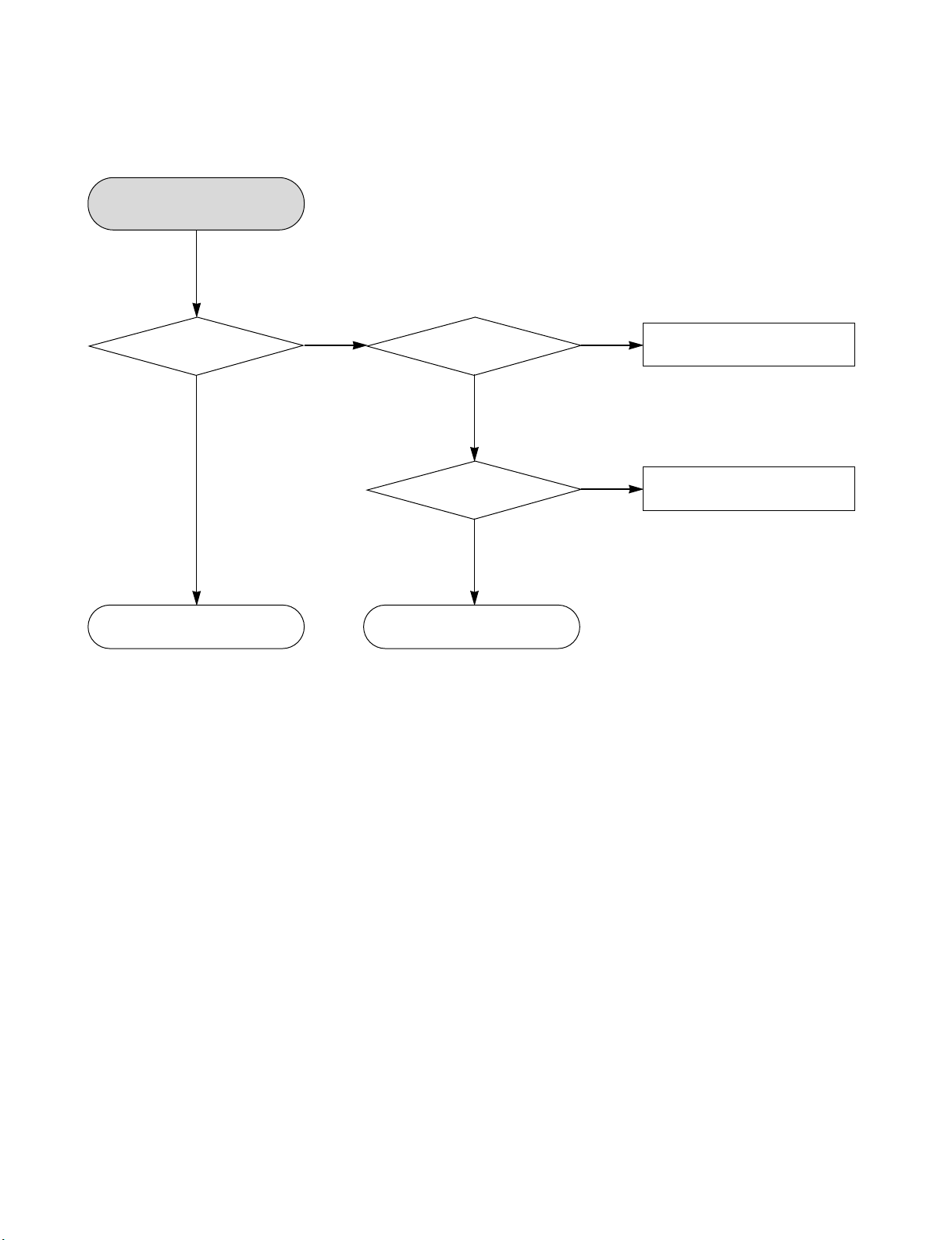
ELECTRICAL TROUBLESHOOTING GUIDE OF AUDIO PART
5. PWM MODULATION PART
PWM modulation part
YES
Check P7905
9PIN 3.3V
YES
Check IC604 PS9829 VDD PIN
power (3,10,22,29,39,47,56,65,
72,87,94) Check X601 2PIN 3.3V
YES
Check if
X601 12.288MHz is
working.
YES
Check IC604
PS9829 86PIN
CLK input
YES
Check
output of IC100
78KOKF2
21-->PWM_CLK
22-->PWM_DATA
43-->PWM_REST
NO
NO
NO
NO
Refer to SMPS
Troubleshooting
Check the
related part of X601
YES
OK
Check R668(470Ω)
output
YES
OK
Check
resistance
output of LINE DATA:
R623 CLK: R624
RST: R619
NO
NO
NO
Replace the related part
Replace the related part
Replace the related part
YES
Check
IC604
PS9829 DATA input
78 PIN-->DATA
79 PIN-->CLK
96 PIN-->REST
YES
Check PWM
MODULATOR
output FL:75(+)74(-)
FR:71(+)70(-)
YES
NO
NO
YES
OK
Check
DVD ASS`Y PS9829
communication condition
(DVD INTERFACE)
YES
Check IC604
PS9829 DATA input
YES
OK
Check IC604 PS9829 part.OK
3-5
NO
NO
Refer to DVD
Troubleshooting
Check resistance
output of each LINE
ELECTRICAL TROUBLESHOOTING GUIDE OF AUDIO PART
6. POWER AMP PART CHECK
Power AMP part check
YES
P7905 3PIN +
13, 14, 15PIN 21.5V
YES
Check input power IC700
34, 29, 26, 21PIN.
YES
Check input power of IC700,
1, 36, 17, 18, 19PIN +12V
YES
Check PWM MODULATOR
input 4, 6, 14, 16PIN
YES
Check POWER IC 700 34,
29, 27, 20PIN output.
NO
NO
Refer to SMPS
Troubleshooting
Check resistance power
IC700: R702, 701, 726, 727, 724
YES
Check output LINE COIL
YES
OK
NO
Replace the related parts
3-6
ELECTRICAL TROUBLESHOOTING GUIDE OF AUDIO PART
7. PORTABLE FUNCTION
Portable function
YES
Check if JK305 contacts with
YES
Check IC200
(BU4052) 4, 11PIN input
waveform.
YES
Check IC200 (BU4052)
3, 13PIN output waveform.
YES
Check IC801
(MC4580) 2, 6PIN input
waveform.
YES
NO
NO
Check IC200
(BU4052) 16PIN V
8PIN VSS power.
Replace the related parts
Check IC801
(MC4580) 4PIN V
8PIN V
DD power.
Replace the related parts.OK
YES
YES
DD
SS,
,
NO
NO
Check u-COM (IC100)
3, 69PIN communication.
Refer to SMPS
Troubleshooting.
3-7
ELECTRICAL TROUBLESHOOTING GUIDE OF AUDIO PART
8. TV-AUDIO FUNCTION
TV-Audio function
YES
Check Video out
YES
Check Audio in
YES
Check IC200
(BU4052) 5, 14PIN
input waveform
YES
Check IC200
(BU4052) 3, 13PIN
output waveform
NO
NO
Check SW4S1
Check IC200
(BU4052) 16PIN VDD
8PIN VSSpower
YES
Replace the related parts.
,
NO
Check u-COM
3, 6PIN communication
YES
Check IC801
(MC4580) 2, 6PIN
waveform
YES
OK
NO
Check IC801
(MC4580) 4PIN VSS,
8PIN VDD power
YES
Replace the related parts.
3-8
NO
Refer to SMPS
Troubleshooting.
ELECTRICAL TROUBLESHOOTING GUIDE OF AUDIO PART
9. TUNER FUNCTION CHECK
TUNER function check
YES
TUNER module (TUN800)
Check
is working.
YES
Check IC200
(BU4052) 1, 12PIN input
waveform.
YES
Check IC200 (BU4052)
3, 13PIN output waveform.
YES
Check IC801
(MC4580) 2, 6PIN input
waveform.
NO
NO
NO
Check TUNER MODUEL
power (Check 2PIN 9V)
Check IC200
(BU4052) 16PIN VDD,
8PIN VSS power
YES
Replace the related parts
Check IC801
(MC4580) 4PIN VSS,
8PIN VDD power
NO
NO
Check u-COM (IC100)
3, 69PIN communication.
Refer to SMPS
Troubleshooting.
OK
YES
YES
Replace the related parts.
3-9
ELECTRICAL TROUBLESHOOTING GUIDE OF AUDIO PART
10. SMPS POWER TROUBLESHOOTING
No. 5.6VA
YES
Is the F101 Normal?
YES
Is the BD101Normal?
YES
Is the TH101 Normal?
YES
NO
NO
NO
Replace the F101 (Use the same Fuse)
Replace the BD101
Replace the R101
Is Vcc (9V ~ 18V)
supplied to IC101
2PIN?
YES
IS the D959 normal?
YES
Is there about 2.5V
at the IC103 1PIN?
YES
Is the IC102 normal?
YES
Is the D947 Normal?
YES
Is the D949 Normal? Replace the D949
YES
Is the D940 Normal?
NO
NO
NO
NO
NO
NO
NO
Is the D102 normal?
NO
Check or Replace the D102
Replace the D959
Replace the IC103
Replace the IC102
Replace the D947
Replace the D940
YES
Is the D943 Normal?
YES
Is the D941 Normal?
YES
Power Line of Main PCB is short
NO
NO
Replace the D943
Replace the D941
3-10
ELECTRICAL TROUBLESHOOTING GUIDE OF AUDIO PART
No 5.0V
YES
Is the Vcc(5.6V)
supplied to IC957
1PIN?
YES
Is the IC957 4PIN “H”?
YES
Check or Replace the IC957
No 3.3V
YES
Is the Vcc(4.2V)
supplied to IC955
1PIN?
YES
Is the IC955 4PIN “H”?
NO
NO
NO
NO
Check or Replace the D959
Check the CD CTL “H”
signal from µ-com
Check or Replace the D943
Check the P CTL “H”
signal from µ-com
YES
Check or Replace the IC955
No 12V
YES
Is the Vcc(13.5V)
supplied to IC947
1PIN?
YES
Is the IC947 4PIN “H”?
YES
Check or Replace the IC947
NO
NO
Check or Replace the D940
Check the P CTL “H”
signal from µ-com
3-11
ELECTRICAL TROUBLESHOOTING GUIDE OF AUDIO PART
No -12V
YES
Is the voltage of
C932 -13V
YES
Is the IC155 2PIN
12V?
YES
Check or Replace the Q942
No VF+
YES
Is the ZD950
Normal?
YES
Replace the R993 or Q950, Q943
NO
NO
NO
Check or Replace the D970
Check the PWR CTL
“H” signal from µ-com
Replace the ZD950
3-12
ELECTRICAL TROUBLESHOOTING GUIDE OF AUDIO PART
11. BLUETOOH PART (OPTIONAL PART)
Check bluetooth module
YES
Check IC200
(BU4052) 2, 15PIN input
waveform.
YES
Check IC200 (BU4052)
3, 13PIN output waveform.
YES
Check IC801
(MC4580) 2, 6PIN input
waveform.
YES
NO
NO
Check IC200
(BU4052) 16PIN V
8PIN VSS
Replace the related parts
Check IC801
(MC4580) 4PIN V
8PIN V
DD power
Replace the related parts.
power
YES
YES
DD
SS,
,
NO
NO
Check u-COM (IC100)
3, 69PIN communication.
Refer to SMPS
Troubleshooting.
OK
3-13
 Loading...