

Page 1
MODEL : MBD-K203Q (FBS203V)
SERVICE MANUAL
P/NO : AFN542679853 MARCH, 2008
KARAOKE MINI
Hi-Fi SYSTEM
SERVICE MANUAL
CAUTION
BEFORE SERVICING THE UNIT, READ THE “SAFETY PRECAUTIONS” IN THIS MANUAL.
MODEL : MBD-K203Q (FBS203V)
Website http://biz.lgservice.com
Internal Use Only
Page 2

1-1
Copyright © 2008 LG Electronics. Inc. All right reserved.
Only for training and service purposes
LGE Internal Use Only
[CONTENTS]
❍ SECTION 1. GENERAL
• SERVICING PRECAUTIONS ................................................................................................ 1-2
• ESD PRECAUTIONS ............................................................................................................ 1-4
• SERVICE INFORMATION FOR EEPROM ............................................................................ 1-5
• PROGRM DOWNLOAD GUIDE ............................................................................................ 1-7
• SPECIFICATIONS .............................................................................................................. 1-11
❍ SECTION 2. EXPLODED VIEWS
• CABINET AND MAIN FRAME SECTION.............................................................................. 2-1
•
DECK MECHANISM EXPLODED VIEW................................................................................ 2-3
•
SPEAKER EXPLODED VIEW .............................................................................................. 2-5
• PACKING ACCESSORY
VIEW.............................................................................................. 2-6
❍ SECTION 3. ELECTRICAL PART
• TROUBLESHOOTING GUIDE
AUDIO PART TROUBLESHOOTING GUIDE ........................................................................ 3-1
DVD PART TROUBLESHOOTING GUIDE .......................................................................... 3-11
• WAVEFORMS OF MAJOR CHECK POINT ........................................................................ 3-19
• WIRING DIAGRAM .............................................................................................................. 3-25
• BLOCK DIAGRAM .............................................................................................................. 3-26
• CIRCUIT DIAGRAMS .......................................................................................................... 3-27
• INTERNAL BLOCK DIAGRAM OF IC ................................................................................ 3-47
• CIRCUIT VOLTAGE CHART ................................................................................................ 3-63
• PRINTED CIRCUIT DIARGAMS ........................................................................................ 3-67
❍ SECTION 4. REPLACEMENT PARTS LIST ................................................................ 4-1
Page 3
1-2
Copyright © 2008 LG Electronics. Inc. All right reserved.
Only for training and service purposes
LGE Internal Use Only
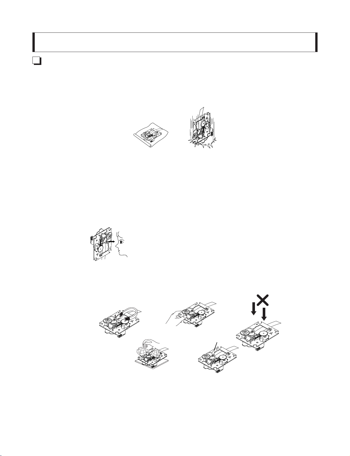
SERVICING PRECAUTIONS
NOTES REGARDING HANDLING OF THE PICK-UP
1. Notes for transport and storage
1) The pick-up should always be left in its conductive bag until immediately prior to use.
2) The pick-up should never be subjected to external pressure or impact.
2. Repair notes
1) The pick-up incorporates a strong magnet, and so should never be brought close to magnetic materials.
2) The pick-up should always be handled correctly and carefully, taking care to avoid external pressure and
impact. If it is subjected to strong pressure or impact, the result may be an operational malfunction and/or
damage to the printed-circuit board.
3) Each and every pick-up is already individually adjusted to a high degree of precision, and for that reason
the adjustment point and installation screws should absolutely never be touched.
4) Laser beams may damage the eyes!
Absolutely never permit laser beams to enter the eyes!
Also NEVER switch ON the power to the laser output part (lens, etc.) of the pick-up if it is damaged.
5) Cleaning the lens surface
If there is dust on the lens surface, the dust should be cleaned away by using an air bush (such as used
for camera lens). The lens is held by a delicate spring. When cleaning the lens surface, therefore, a cotton
swab should be used, taking care not to distort this.
6) Never attempt to disassemble the pick-up.
Spring by excess pressure. If the lens is extremely dirty, apply isopropyl alcohol to the cotton swab.
(Do not use any other liquid cleaners, because they will damage the lens.) Take care not to use too much
of this alcohol on the swab, and do not allow the alcohol to get inside the pick-up.
Storage in conductive bag
Drop impact
NEVER look directly at the laser beam, and don’t allow
contact fingers or other exposed skin.
Magnet
How to hold the pick-up
Conductive Sheet
Cotton swab
Pressure
Pressure
SECTION 1. GENERAL
Page 4
1-3
Copyright © 2008 LG Electronics. Inc. All right reserved.
Only for training and service purposes
LGE Internal Use Only
NOTES REGARDING COMPACT DISC PLAYER REPAIRS
1. Preparations
1) Compact disc players incorporate a great many ICs as well as the pick-up (laser diode). These components
are sensitive to, and easily affected by, static electricity. If such static electricity is high voltage, components
can be damaged, and for that reason components should be handled with care.
2) The pick-up is composed of many optical components and other high-precision components. Care must be
taken, therefore, to avoid repair or storage where the temperature of humidity is high, where strong magnetism is present, or where there is excessive dust.
2. Notes for repair
1) Before replacing a component part, first disconnect the power supply lead wire from the unit
2) All equipment, measuring instruments and tools must be grounded.
3) The workbench should be covered with a conductive sheet and grounded.
When removing the laser pick-up from its conductive bag, do not place the pick-up on the bag. (This is
because there is the possibility of damage by static electricity.)
4) To prevent AC leakage, the metal part of the soldering iron should be grounded.
5) Workers should be grounded by an armband (1M Ω)
6) Care should be taken not to permit the laser pick-up to come in contact with clothing, in order to prevent static electricity changes in the clothing to escape from the armband.
7) The laser beam from the pick-up should NEVER be directly facing the eyes or bare skin.
Resistor
(1 Mohm)
Conductive
Sheet
Resistor
(1 Mohm)
Armband
Page 5
1-4
Copyright © 2008 LG Electronics. Inc. All right reserved.
Only for training and service purposes
LGE Internal Use Only
Electrostatically Sensitive Devices (ESD)
Some semiconductor (solid state) devices can be damaged easily by static electricity. Such components
commonly are called Electrostatically Sensitive Devices (ESD). Examples of typical ESD devices are integrated
circuits and some field-effect transistors and semiconductor chip components. The following techniques should
be used to help reduce the incidence of component damage caused by static electricity.
1. Immediately before handling any semiconductor component or semiconductor-equipped assembly, drain off
any electrostatic charge on your body by touching a known earth ground. Alternatively, obtain and wear a
commercially available discharging wrist strap device, which should be removed for potential shock reasons
prior to applying power to the unit under test.
2. After removing an electrical assembly equipped with ESD devices, place the assembly on a conductive surface
such as aluminum foil, to prevent electrostatic charge buildup or exposure of the assembly.
3. Use only a grounded-tip soldering iron to solder or unsolder ESD devices.
4. Use only an anti-static solder removal device. Some solder removal devices not classified as "anti-static" can
generate electrical charges sufficient to damage ESD devices.
5. Do not use freon-propelled chemicals. These can generate electrical charges sufficient to damage ESD
devices.
6. Do not remove a replacement ESD device from its protective package until immediately before you are
ready to install it. (Most replacement ESD devices are packaged with leads electrically shorted together by
conductive foam, aluminum foil or comparable conductive materials).
7. Immediately before removing the protective material from the leads of a replacement ESD device, touch the
protective material to the chassis or circuit assembly into which the device will by installed.
CAUTION : BE SURE NO POWER IS APPLIED TO THE CHASSIS OR CIRCUIT, AND OBSERVE ALL OTHER
SAFETY PRECAUTIONS.
8. Minimize bodily motions when handing unpackaged replacement ESD devices. (Otherwise harmless motion
such as the brushing together of your clothes fabric or the lifting of your foot from a carpeted floor can generate static electricity sufficient to damage an ESD device).
CAUTION. GRAPHIC SYMBOLS
THE LIGHTNING FLASH WITH APROWHEAD SYMBOL. WITHIN AN EQUILATERAL TRIANGLE, IS
INTENDED TO ALERT THE SERVICE PERSONNEL TO THE PRESENCE OF UNINSULATED
“DANGEROUS VOLTAGE” THAT MAY BE OF SUFFICIENT MAGNITUDE TO CONSTITUTE A RISK OF
ELECTRIC SHOCK.
THE EXCLAMATION POINT WITHIN AN EQUILATERAL TRIANGLE IS INTENDED TO ALERT THE
SERVICE PERSONNEL TO THE PRESENCE OF IMPORTANT SAFETY INFORMATION IN SERVICE
LITERATURE.
SAFETY PRECAUTIONS
Page 6
1-5
Copyright © 2008 LG Electronics. Inc. All right reserved.
Only for training and service purposes
LGE Internal Use Only
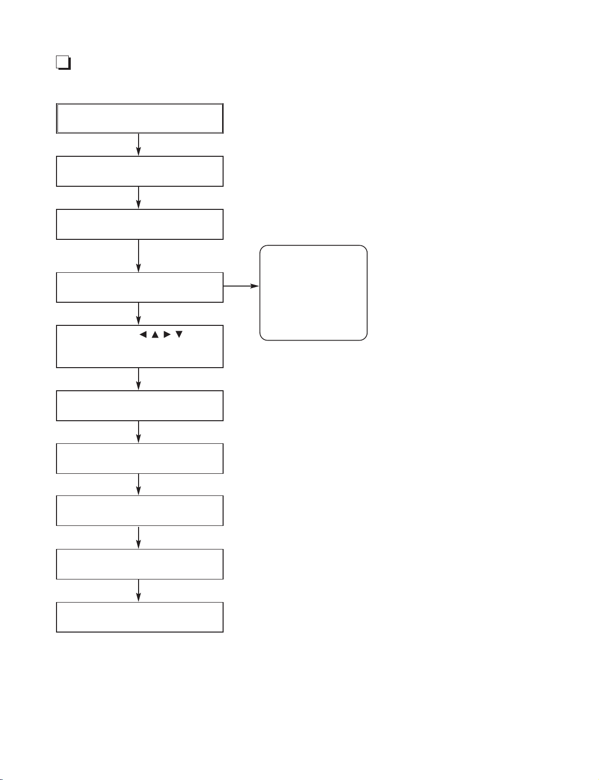
SERVICE INFORMATION FOR EEPROM (MICOM PART)
POWER ON
FLD no disc status
Remote control ‘2’ + Front ‘STOP’
push same timing during 5s
FLD ‘OP-0….
Use arrow key ( ) move
to appropriate position and make
changes
Press ENTER key once
FLD ‘write ok’
Remote control ‘2’ + Front ‘STOP’
push same timing
FLD display E2P CLR or EP CLR
Auto power off
MODEL : FBD203
NAME HEX
OPT 1 00
OPT 2 00
OPT 3 00
OPT 4 00
OPT 5 00
DETECT NEW EEPROM
(OPTION EDIT SCREEN)
Page 7
1-6
Copyright © 2008 LG Electronics. Inc. All right reserved.
Only for training and service purposes
LGE Internal Use Only
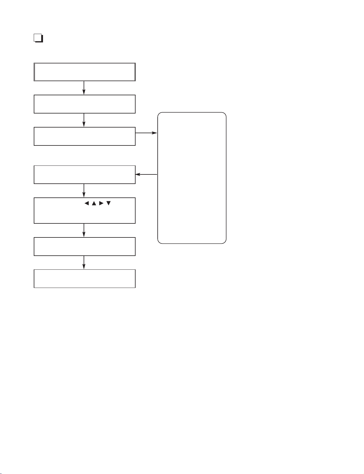
SERVICE INFORMATION FOR EEPROM (DVD PART)
POWER ON
DVD LOGO Status (NO Disk status)
Remote control
Pause key-->1-->4-->7-->2 in order.
Press number 0~9, Press character
A~F (1~6 for a while)
Use arrow key ( ) to
move to appropriate position and
make changes
Press pause key once
Change will be applied when power
OFF-->ON.
NAME
OPT 1
OPT 2
OPT 3
OPT 4
OPT 5
OPT 6
OPT 7
OPT 8
OPT 9
OPT A
OPT B
OPT C
OPT D
OPT E
OPT F
OPT G
HEX
00
00
00
00
00
00
00
00
00
00
00
00
00
00
00
00
DETECT NEW EEPROM
(OPTION EDIT SCREEN)
Page 8
1-7
Copyright © 2008 LG Electronics. Inc. All right reserved.
Only for training and service purposes
LGE Internal Use Only
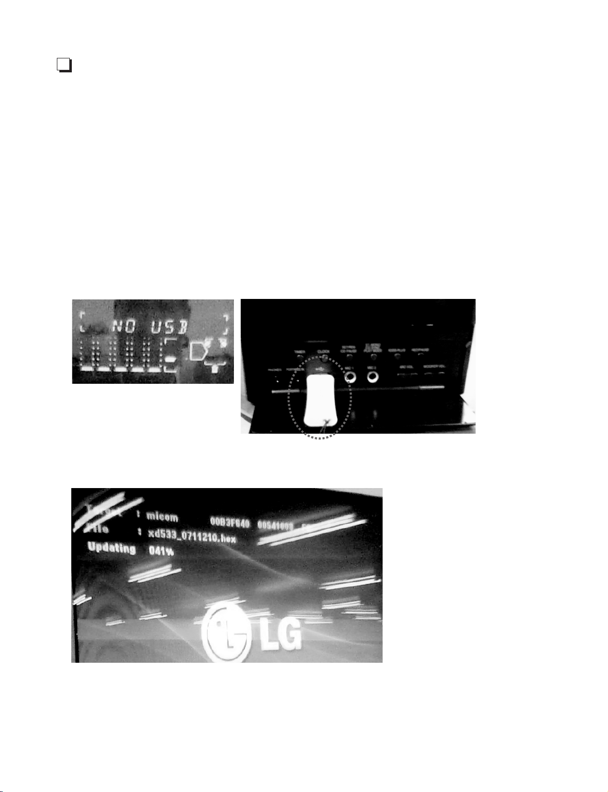
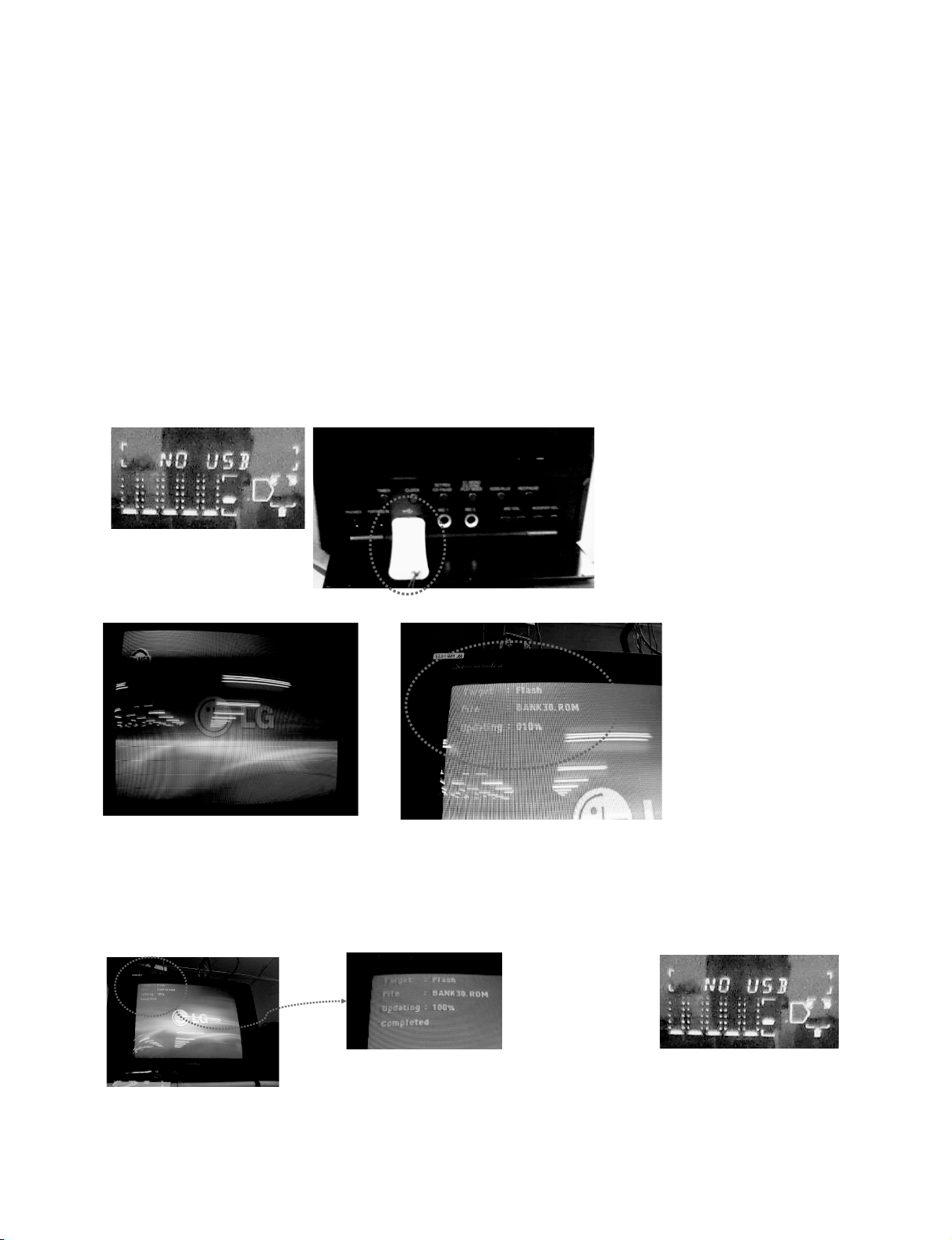
PROGRM DOWNLOAD GUIDE
• AUDIO USB DOWNLOAD GUIDE
The name of the program file to download is FBD203_date.hex.
- At some PCs with the security program (Water Wall) installed, store it at the USB device, disable
the security protection, and download it to the set.
Note) Do not perform any other work such as disconnecting the USB device, switching to the
other Function and turning off the power while downloading it to the set.
The USB device should be disconnected after completing the download.
1. When the USB device is inserted at the USB function a after a while TV screen is displayed on the
as following figure.
Page 9
1-8
Copyright © 2008 LG Electronics. Inc. All right reserved.
Only for training and service purposes
LGE Internal Use Only
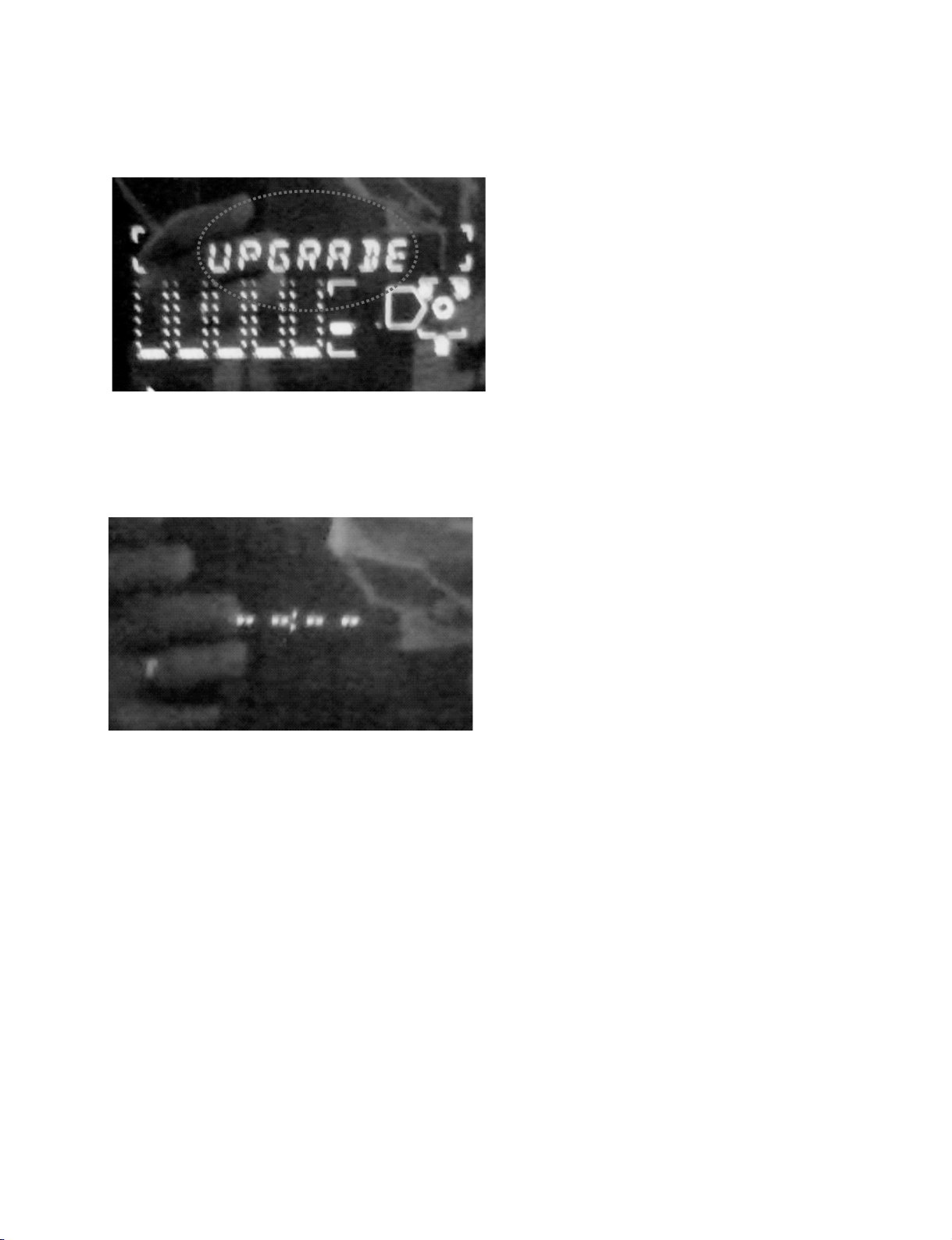
2. The message “Upgrade” is displayed while downloading.
3. The power is automatically turned off when downloading is completed.
Page 10
1-9
Copyright © 2008 LG Electronics. Inc. All right reserved.
Only for training and service purposes
LGE Internal Use Only
• DVD USB DOWN LOAD GUIDE
The program file to download should be named as BANK30.ROM.
- The downloaded file should be modified as BANK30.ROM to use.
- At some PCs with the security program (Water Wall) installed, store BANK30.ROM at the USB
device, disable the security protection, and download it to the set.
- After safely storing BANK30. ROM at the USB device, perform the following steps.
Note) Do not perform any other work such as disconnecting the USB device, switching to the
other Function and turning off the power while downloading it to the set.
1. When the USB device is inserted at the USB functiona after a while TV screen is displayed on the
as following figure.
2. When downloading is completed, the message “Completed” is displayed at the top left of the TV screen
as shown at Figure(1).
If the message “NO USB” is displayed as shown at Figure(2), downloading is completed.
FIG.1
FIG.2
Page 11
1-10
Copyright © 2008 LG Electronics. Inc. All right reserved.
Only for training and service purposes
LGE Internal Use Only
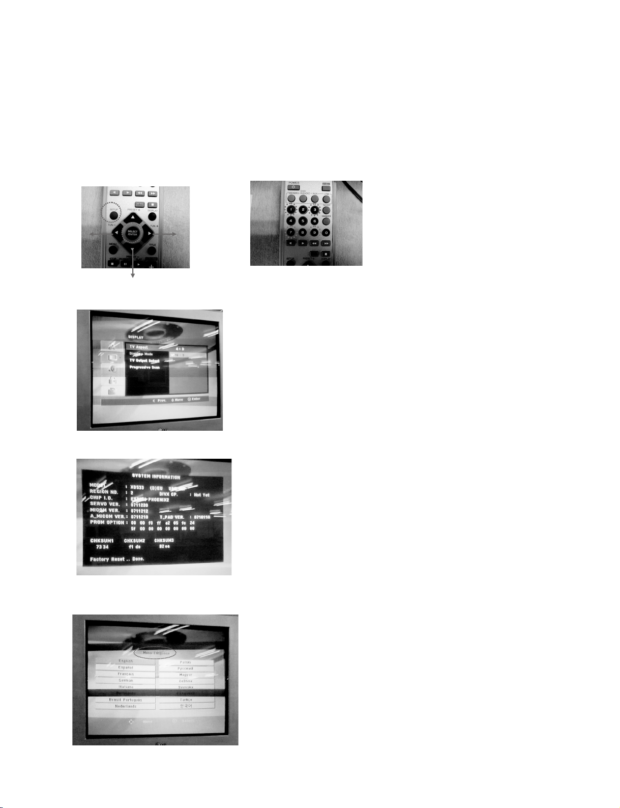
3. Turn on the power, press the SETUP button of the remote controller at the USB FUNCTION.
When the SETUP window is displayed on the screen, move down once to select the DISPLAY menu.
Go to the TV Aspect at the right menu, move to “16:9”, enter “1397139” by using the numeric key of the
remote controller, and then press the Enter key.
Then, the System Information screen is displayed as shown inthe following figure. If not, retry the steps
at the above.
4. When Step 3 is completed, press the PAUSE KEY of the remote controller.
5. Disconnect the power code, and reconnect it after 5 seconds to complete downloading.
7. When the power is turned on again, the language selection menu is initially displayed.
After selecting the desired language, press the SELECT/ENTER.
Left Right
Down
Page 12

1-11
Copyright © 2008 LG Electronics. Inc. All right reserved.
Only for training and service purposes
LGE Internal Use Only
SPECIFICATIONS
General
Power supply Refer to main label.
Power consumption Refer to main label.
Net Weight 3.42 kg
External dimensions (W x H x D) 330 x 138.5x 252.4 mm
Operating conditions Temperature: 5° C to 35° C, Operation status: Horizontal
Operating humidity 5% to 85%
Tuner
FM Tuning Range 87.5 - 108.0 MHz or 65.0 - 74.0 MHz, 87.5 - 108.0 MHz
Intermediate Frequency 10.7 MHz
AM Tuning Range 522 - 1,620 kHz or 520 - 1,720 kHz
Intermediate Frequency 450 kHz
Amplifier
OUTPUT POWER 100 W + 100 W (4Ω, THD 0.5%) : MBD- K203Q
50 W + 50 W( 4Ω, THD 0.5%) : MBD- K103Q
Stereo Mode 100 W + 100 W (4Ω, THD 0.5%) : MBD- K203Q
50 W + 50 W( 4Ω, THD 0.5%) : MBD- K103Q
Frequency Response 40 - 20000Hz
Signal- to- noise ratio 75dB
DVD/ VCD/ CD player
Frequency response (audio) 40 - 20000 Hz
Signal- to- noise ratio (audio) More than 75 dB (1 kHz)
Signal- to- noise ratio (video) More than 55 dB (1 kHz)
Dynamic range (audio) More than 80 dB
Video output 1.0 V (p- p), 75 Ω
Component Video output (Y) 1.0 V (p- p), 75 Ω
Speakers
FBS203V
Type 2Way 2Speaker
Impedance 4 Ω
Rated Input Power 100 W
Max. Input Power 200W
Net Dimensions (W x H x D) 165 X 341 X 261 mm
Net Weight 4.48 kg
Designs and specifications are subject to change without pior notice.
Page 13
1-12
Copyright © 2008 LG Electronics. Inc. All right reserved.
Only for training and service purposes
LGE Internal Use Only
Page 14
2-1 2-2
Copyright © 2008 LG Electronics. Inc. All right reserved.
Only for training and service purposes
LGE Internal Use Only
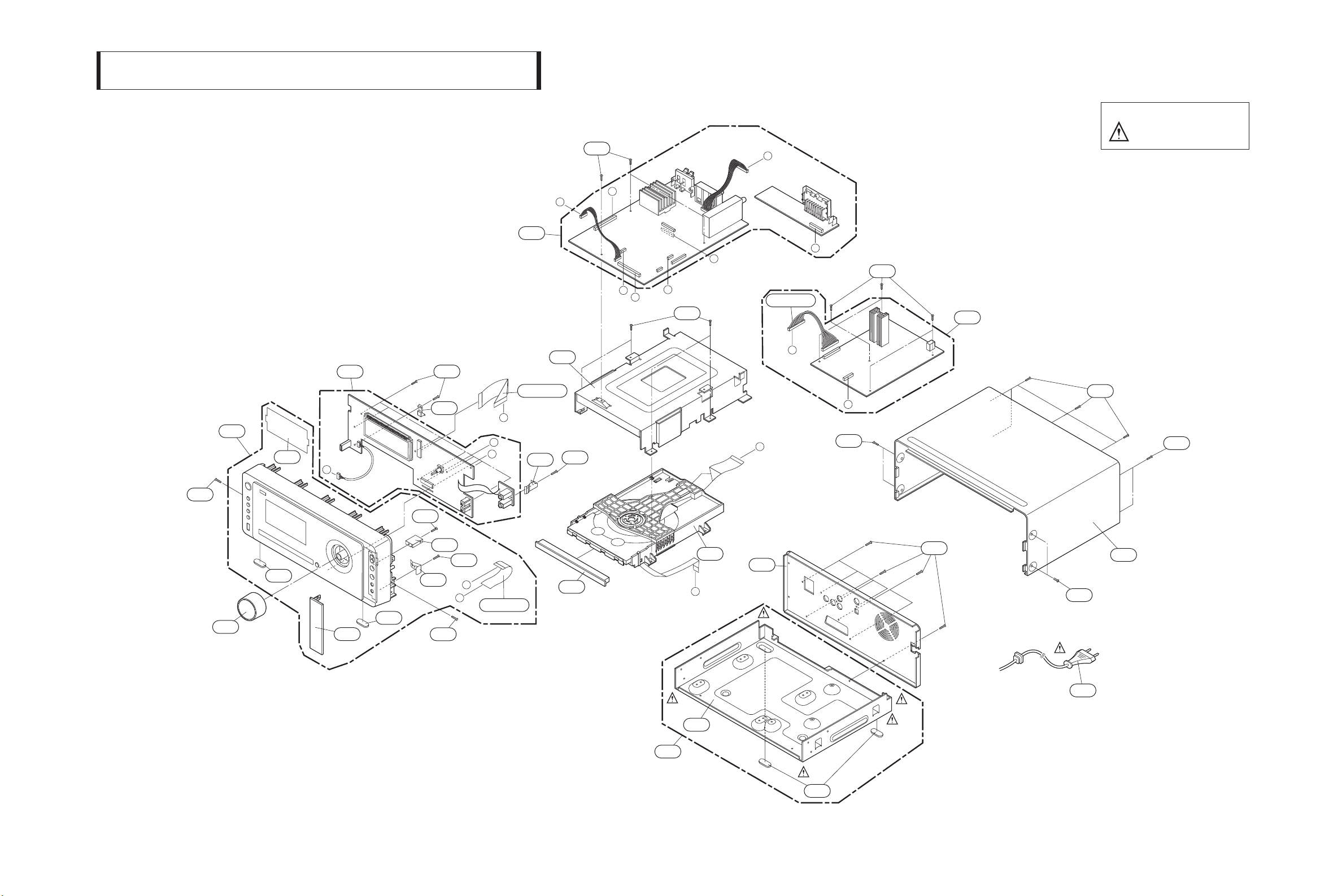
• CABINET AND MAIN FRAME SECTION
SECTION 2. EXPLODED VIEWS
453
NOTES) THE EXCLAMATION POINT WITHIN AN
EQUILATERAL TRIANGLE IS INTENDED
TO ALERT THE SERVICE PERSONNEL
TO THE PRESENCE OF IMPORTANT
SAFETY INFORMATION IN SERVICE
B
LITERATURE.
453
A42
257
A46
A
C
MAIN
E
SCART
B
471
F
273
A43
453
CABLE2
259
FRONT
F
MIC
G
H
I
258
453
D
G
471
CABLE1
A47
C
SMPS
453
A
E
453
453
453
271
254
253
271
255
256
453
453
H
I
CABLE3
260
A26
272
D
270
A44
271
465
250
453
300
Page 15
2-3 2-4
Copyright © 2008 LG Electronics. Inc. All right reserved.
Only for training and service purposes
LGE Internal Use Only
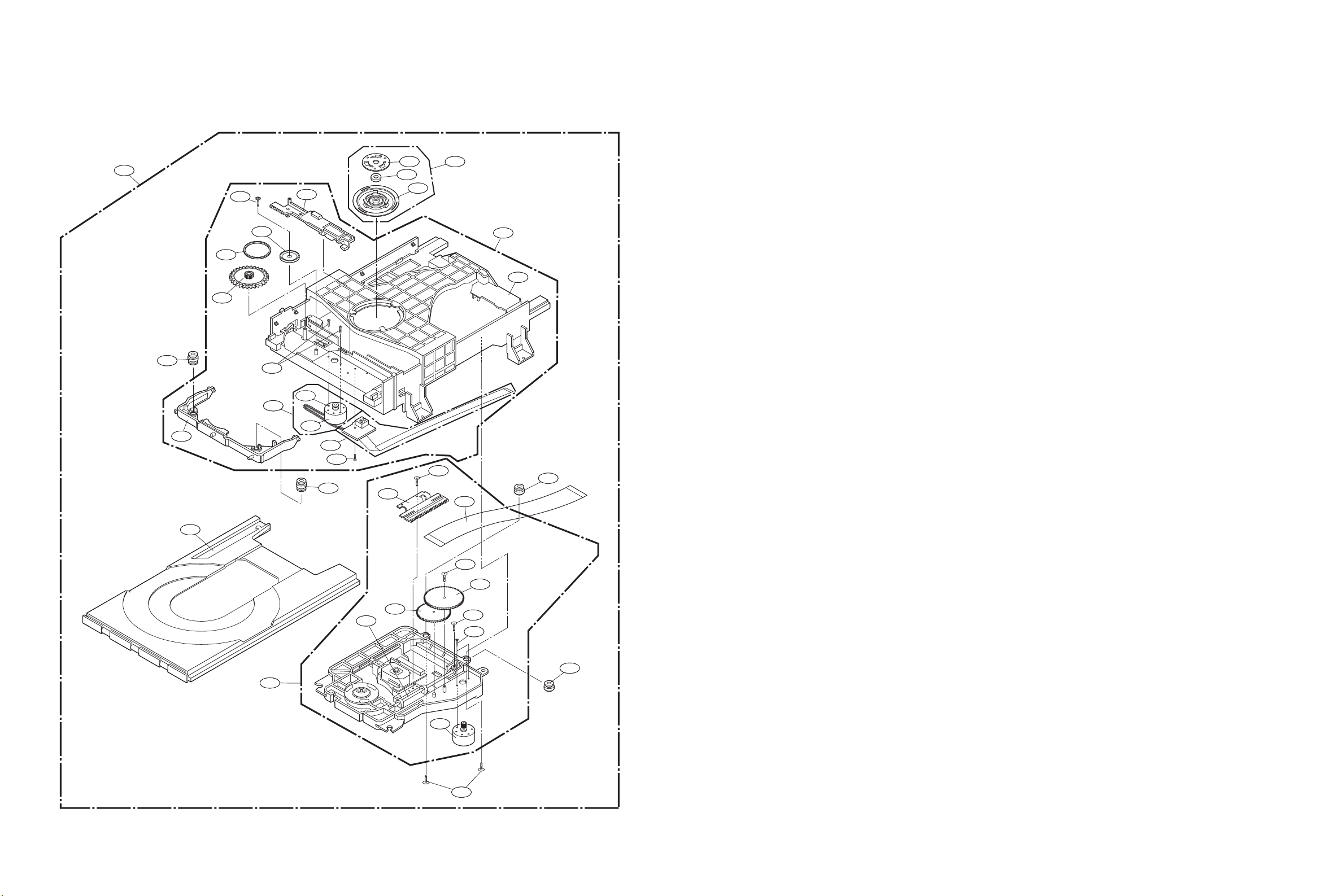
DECK MECHANISM EXPLODED VIEW
1. DECK MECHANISM SECTION (DP-10)
A26
012
019
013
017
439
014
435
015
018
015B
015A
016
012
440
030
001
002
003
432
A01
A02
020
012A
010
026
A03
036
025
021
439
430
431
435
024
012A
Page 16
2-5
Copyright © 2008 LG Electronics. Inc. All right reserved.
Only for training and service purposes
LGE Internal Use Only
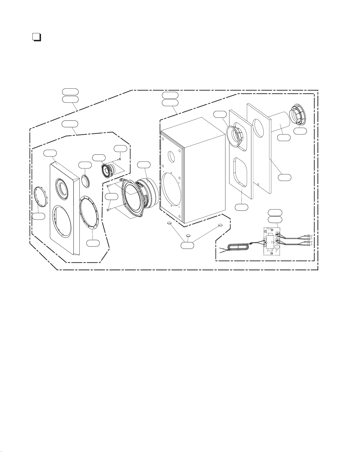
• FRONT SPEAKER (FBS203V)
SPEAKER EXPLODED VIEW
851
852
A80L
A80R
A81A
853
854
A81L
A81R
860
860
863
858
857
856
862
855
861
865L
865R
859
Page 17
2-6
Copyright © 2008 LG Electronics. Inc. All right reserved.
Only for training and service purposes
LGE Internal Use Only
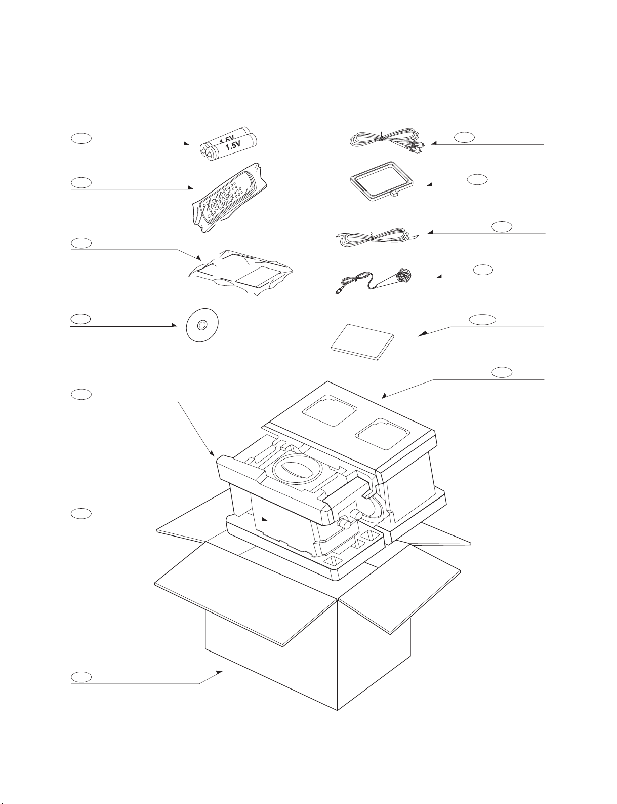
• PACKING ACCESSORY
VIEW
808 Battery
900 Remote Control
801 Instruction Ass'y
811
Plug Ass'y, 1Way
Antenna Loop
824
827
825 Antenna
Micro Phone
832
DISC
803 Packing
804 Bag
801S
Song Book
803 Packing
802 Box
Page 18
3-1
Copyright © 2008 LG Electronics. Inc. All right reserved.
Only for training and service purposes
LGE Internal Use Only
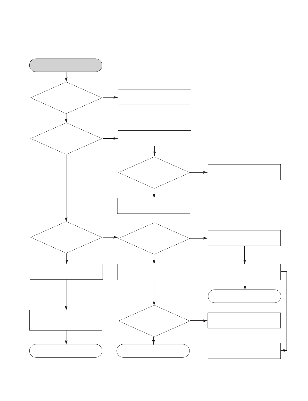
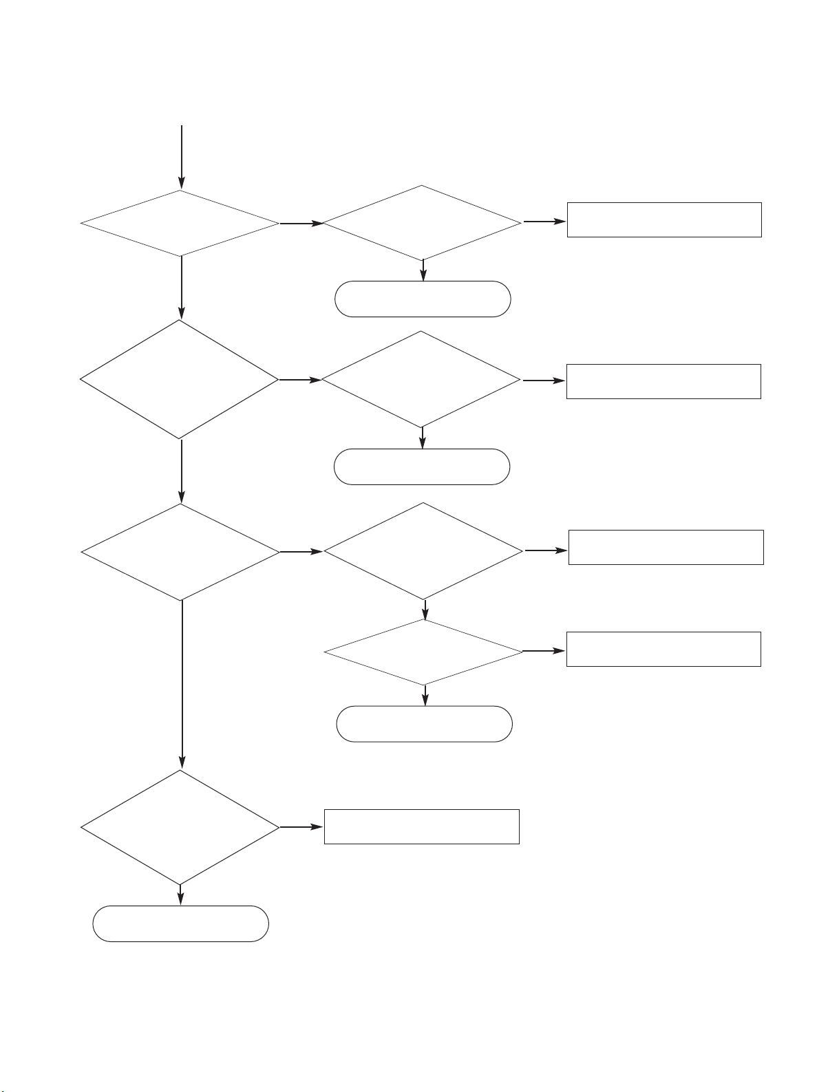
1. MICOM PART CHECK I
OK OK
NO
NO NO
Replace the
related parts.
Check if output voltage
of IC101 KIA7042 is
4.3V.
YES
YES
YES YES
YES YES
Check IC100
LC87F5NC8A 4 PIN
power.
YES
Refer to SMPS
troubleshooting.
MICOM PART
HECK I
Check
CN101 6PIN
P-SENS.
NO
Check
power of both
terminals of IC101
KIA7042
Check if
IC101 KIA7042
input is over 5V.
Check the
related part of IC101
KIA7042.
AUDIO ELECTRICAL TROUBLESHOOTING GUIDE
SECTION 3. ELECTRICAL PART
Page 19
3-2
Copyright © 2008 LG Electronics. Inc. All right reserved.
Only for training and service purposes
LGE Internal Use Only
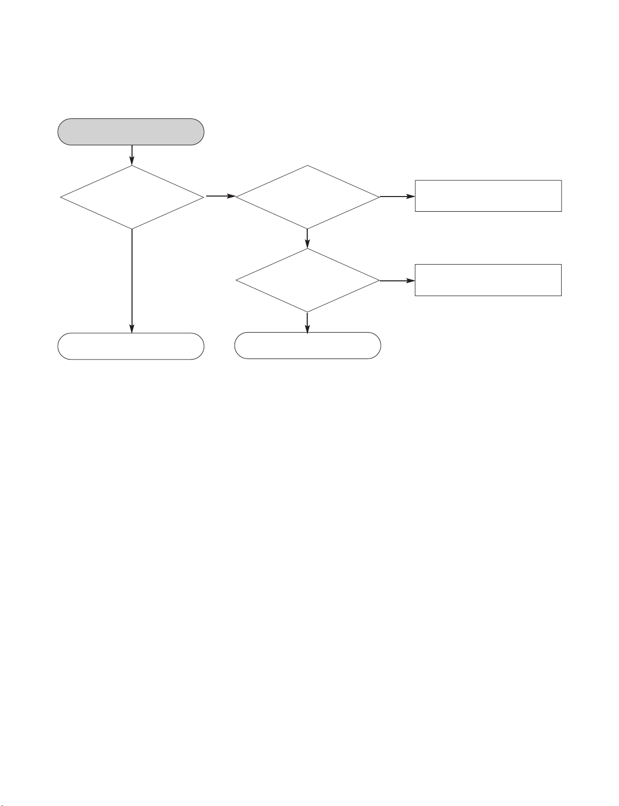
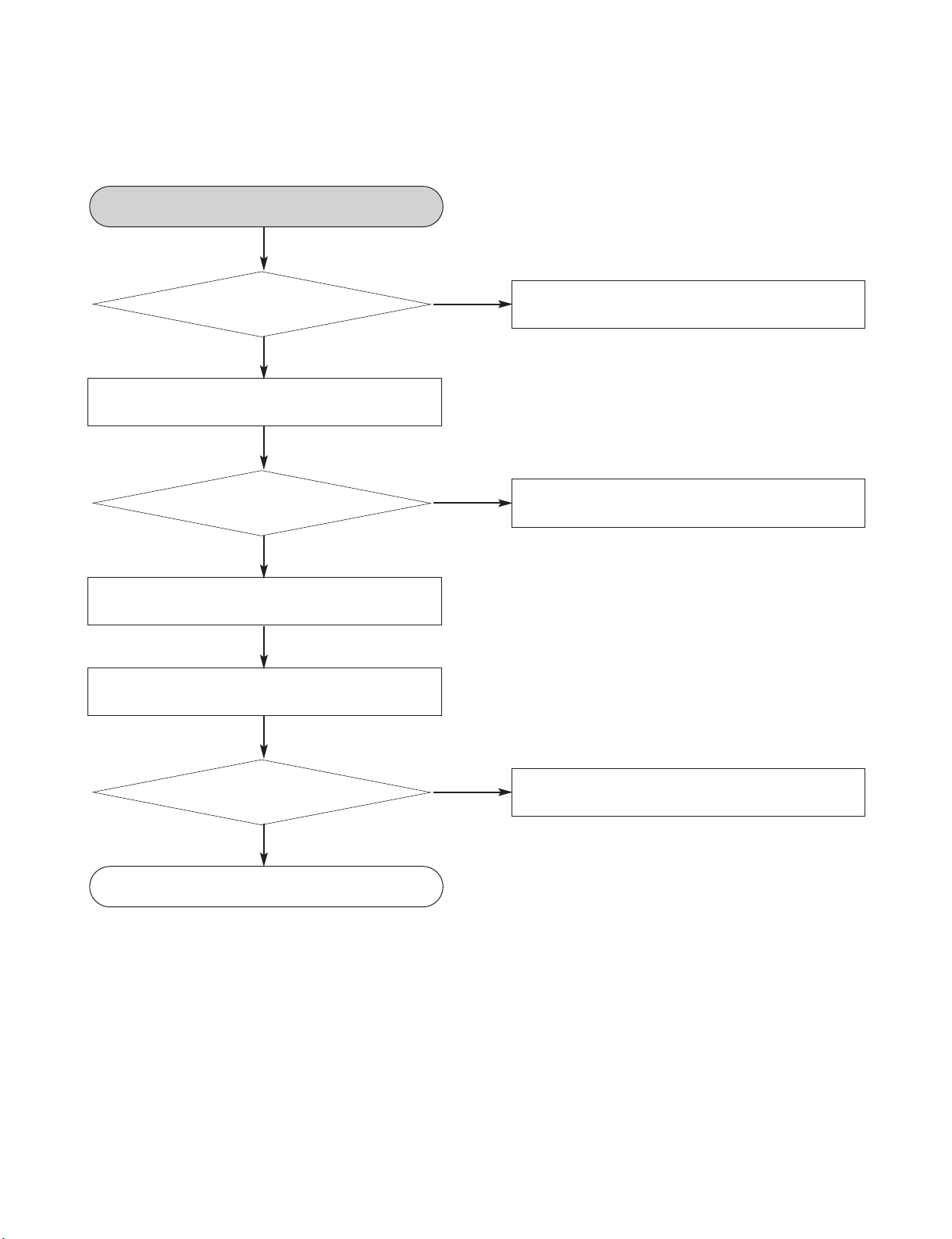
2. MICOM PART CHECK II
NO
YES
YES
YES
YES
YES
Refer to SMPS
Troubleshooting.
NO
Check D101 RS1G
output is working on 5V.
Check IC103 8PIN IC100
14,55,89 PIN 5V
YES
YES
OK
YES
YES
Check Q102 COLLECTOR
YES
Check the related part.
Replace the related parts.
Check the working condition
X100:32.768kHz
X101:9.8304MHz
Check CN101 5PIN 5.6V
Check power
of both terminals of D101
RS1G.
YES
NO
Check Q10
EMITTER 5V and
COLLECTOR 5V
Check the related part
MICOM PART CHECK II
NO
NO
Replace the related parts.
Check Q102 BASE
PIN 0.6V HIGH
NO
Check output power of IC101
KIA7042 is over 4.3V.
Check the
related part.
NO
Replace the related parts.
OK
YES
OK
YES
OK
Page 20
3-3
Copyright © 2008 LG Electronics. Inc. All right reserved.
Only for training and service purposes
LGE Internal Use Only
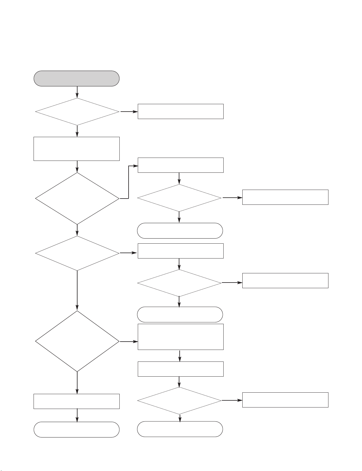
3. IC103 S-24CS16A01 PART CHECK
YES
YES
YES
YES
81 PIN DATA 82 PIN CLK
Check the related part.
NO
Check MICOM power 5V
CHECK IC100 LC87F5NC8A
81,82 PIN
NO
Replace the related parts.
NO
Refer to micom
troubleshooting.
OK
OK
Page 21
3-4
Copyright © 2008 LG Electronics. Inc. All right reserved.
Only for training and service purposes
LGE Internal Use Only
4. FLD DISPLAY PART CHECK
NO
YES
YES
YES
YES
Refer to SMPS
Troubleshooting
NO
Replace the related part
Check P3101 assembly
F1+,F2-both terminals:over
3.7V Check power VKK:over
-28V.
YES
FLT light on?
Check
CN101 1,2,3 power.
YES
Check
P3101 connection
condition and power F1+,F2-
both terminals:over 3.7V
Check power VKK:over -28V
Check 4,5 PIN:5.6V
YES
Check
IC304 PT6324
power 50 PIN VKK:-28V
9.52 PIN +5V
YES
YES
Check
power of each PIN.
IC100
Check→IC304
Data communication.
PIN PIN
27PIN→3PIN STB
26PIN→2PIN DO
28PIN→1PIN CLK
OK
OK
OK
NO
Replace the related part.
NO
Replace the related part.
NO
NO
NO
When 5V fails,check D321SR35
input and output power.
IC100 27 PIN→STB
28 PIN→1PIN CLK
Check Data output.
Check 26 PIN→DO
→DATA input.
YES
YES
YES
Check the related part
YES
Check the related part
OK
YES
FLD DISPLAY CHECK
Page 22
3-5
Copyright © 2008 LG Electronics. Inc. All right reserved.
Only for training and service purposes
LGE Internal Use Only
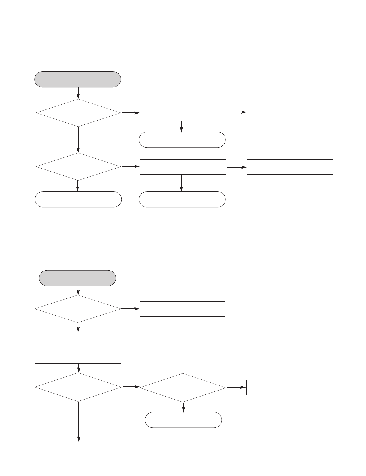
5. TOUCH-PAD PART CHECK
NO
NO
YES
YES
PN3A2 1PIN 5V.
NO
Replace the related part.
NO
Refer to SMPS
Troubleshooting.
Check resistance output of
line CLK :R3A2 DATA :R3A3
IC3A1
28PIN check 5V.
Check
IC3A1 8Pin,9Pin,
IC100 97Pin :CLK,
96Pin :DATA
TOUCH-PAD CHECK
YES
OK
YES
OK
YES
OK
6. PWM MODULATION PART CHECK
Check
PN102 10PIN 3.3V.
PWM MODULATION
PART CHECK
Refer to SMPS
Troubleshooting.
NO
Check if X701
12.288MHz is working.
YES
YES
YES
YES
Check IC702 PS9830 VDD
PIN power (3,10,22,29,39,47,
56,65,72,87,94)Check X701
2PIN 3.3V
Replace the related part.
NO
YES
Check the
related part of
X701.
OK
NO
Page 23
3-6
Copyright © 2008 LG Electronics. Inc. All right reserved.
Only for training and service purposes
LGE Internal Use Only
NO
NO
NO
Check
output of IC100
LC87F5NC8A
21→PWM_CLK
22→PWM_DATA
43→PWM_REST
YES
YES
YES
YES
Check IC702
PS9830 DATA input
78 PIN→DATA
79 PIN→CLK
96 PIN→REST
Check
PWM MODULATOR
output
FL:75(+)74(-)
R:71(+)70(-)
OK
Replace the related part.
NO
Check
resistance output of LINE
DATA:R797
CLK:R795
RST:R790
Refer to DVD Troubleshooting.
NO
Check DVD
ASS`Y PS9830
communication condition
(P7403)
YES
OK
Check IC702 PS9830 part.
Check resistance
output of each LINE.
NO
Check IC702
PS9830 DATA input.
OK
YES
YES
YES
Check IC702 PS9830
86 PIN CLK input
Replace the related part.
NO
YES
Check R791(1M)output
OK
NO
Page 24
3-7
Copyright © 2008 LG Electronics. Inc. All right reserved.
Only for training and service purposes
LGE Internal Use Only
7. PWM AMP PART CHECK
YES
YES
NO
Refer to SMPS Troubleshooting.
PN102
3PIN + 13,14,15 PIN 28V.
YES
YES
NO
Check resistance power
IC700:R702,701,726,727,724.
Check input power of IC700,
1,36,17,18,19 PIN +12V
YES
NO
Replace the related parts.
Check output LINE COIL.
POWER AMP PART CHECK
OK
Check input power IC700
34,29,26,21 PIN.
YES
Check PWM MODULATOR
input 4,6,14,16 PIN.
YES
Check POWER IC 700 34,
29,27,20 PIN output.
Page 25

3-8
Copyright © 2008 LG Electronics. Inc. All right reserved.
Only for training and service purposes
LGE Internal Use Only
8. TUNER FUNCTION PART CHECK
YES
YES
NO
Check TUNER MODUEL
power(Check 4PIN 9V).
Check TUNER
module(TU100)is working.
YES
YES
NO
Check IC201(CS5345)
5,14,30:5V 36,46,:3.3V
Replace the related parts
Check IC201(CS5345)
14PIN output waveform.
TUNER FUNCTION PART CHECK
OK
Check IC201(CS5345)
26,27PIN input waveform.
YES
Page 26

3-9
Copyright © 2008 LG Electronics. Inc. All right reserved.
Only for training and service purposes
LGE Internal Use Only
9. SMPS POWER CIRCUIT
NO
YES
YES
Replace the fuse.
Check the FUSE
F901.
NO
YES
Check BD901,LF901,902.
NO
Check short of P9702 line.
Check short of P9701,P9702 line.
NO
Check short of P9701 line.
NO
Replace IC901,902.
Check
the DC V of C905
if DC V is over
400V.
NO
YES
Check the
DC V of C909,C903,C921
If DC V is in 14~19V
And it is steady
Check IC901,902.
YES
YES
Check the
DC V of C981,C945.
If DC V is 6.1V.
YES
Check the
DC V of C950,C951
If DC V is in
29V.
OK
MAIN PART
MAIN PART
Page 27

3-10
Copyright © 2008 LG Electronics. Inc. All right reserved.
Only for training and service purposes
LGE Internal Use Only
P-SENS VKK PART CHECK
NO
Check power circuit
Troubleshooting.
YES
P-SENS
Check
the PIN6 of P9702
if DC V is over
5.6V
YES
OK
NO
Check power circuit
Troubleshooting.
YES
VKK CHECK
Check
the PIN3 of P9702
if DC V is over
-30V ±1.
YES
OK
10. IPOD PART(ONLY NORTH AMERICA)
YES
YES
YES
YES
YES
NO
Check the JK3C1 13pin, 30pin.
Check the JK3C1 13pin and 30pin line.
LOADING
NO
Check the JK3C1 18pin, 19pin.
Check theJK3C1 18pin and 19pin line
OSD IPOD
TURN ON IPOD
OK
OK
YES
OK
YES
Page 28

3-11
Copyright © 2008 LG Electronics. Inc. All right reserved.
Only for training and service purposes
LGE Internal Use Only
DVD ELECTRICAL TROUBLESHOOTING GUIDE
1. POWER CHECK GUIDE
YES
YES
YES
YES
YES
YES
Does DVD
appear at FLD?
Does No DISC or
Time are appeared at
FLD?
Check Connector
(P4405,P4407,P4408).
NO
NO
Does it
appear DVD ERROR at
FLD?
POWER ON
NO
Check an Audio Micom
Select the DVD Mode
Reconnect it.
YES
Check DVD MD Module.
Check the voltage
of each pin on PN102.
OK
Page 29

3-12
Copyright © 2008 LG Electronics. Inc. All right reserved.
Only for training and service purposes
LGE Internal Use Only
2. TEST & DEBUG FLOW
NO
NO
Check connection lines between
FLASH & ES8390 or the FLASH
access time whether is suitable or not.
YES
Check AV cable connection
to TV set.
Show LOGO?
YESYES
Flash Memory
operates properly?
NO
Check connection lines between
SDRAM.
(IC502) & ES8390 or the SDRAM is
damaged.
YES
SDRAM works
properly?
NO
Check the related circuit of
ES8390 (IC501)
PIN80,83,84,85
YES
ES8390 VIDEO
outputs properly?
NO
NO
Check the MD mecha
Check the cable connection between
DVD PCB and MD (MECHA).
Does DISC was
inserted inside when
you push Disc1~5
button?
YESYES
SW5 & SW7 signals
on PN4402 are OK?
NO
Check the output signal of
ES8390 to IC401 for control
OPEN/CLOSE.
YES
OPEN / CLOSE
signals on IC401 are
OK?
NO
Check the Tray control I/O
Pin on IC401.
YES
Load+ & load- signals
on PN4402 are OK?
POWER ON
A
Page 30

3-13
Copyright © 2008 LG Electronics. Inc. All right reserved.
Only for training and service purposes
LGE Internal Use Only
NO
YES
Check the MD
YES
Check the related circuit of SLED
and Motor driver IC ( IC401)
YES
Check the cable connection
with MECHA.
Do not put in disc and
tray close.
Does the
SLED move to inner side
when it is at outer
position?
YESYES
Motor Drive
DRV_MUTE pin
is high?
YES
YES
SLED signal is OK?
NO
NO
Check Focus connection on
ES8390 and motor driver IC.
Check cable connection
with pick-up head.
Optical
Lens is moving
for searching Focus?
YESYES
Proper
Focus outputs
to motor driver?
NO
Check the motor driver (IC401).
YES
Proper F+ & F-outputs?
A
B
Page 31

3-14
Copyright © 2008 LG Electronics. Inc. All right reserved.
Only for training and service purposes
LGE Internal Use Only
NO
NO
Check the laser power circuit between
ES8390 and power transistor.
(Q405, Q406)
YES
YES
Check cable connection
between PN4401 and pick-up head.
Put disc in SLOT.
Laser turns on
when reading
disc?
YESYES
DVDLD or CDLD
output properly?
NO
Check the related circuit of laser
power transistor.
YES
Collector
voltage of power transistor
is ok? (Q405, Q406)
NO
NO
Check the SPINDLE related
circuit on ES8390
NO
Laser off.
Check the cable connection
between PN4401 and MD.
Does SPINDLE
rotate?
YES
YES
YES
Proper SPINDLE
signal on ES8390.
NO
Check the SPINDLE control of
motor driver IC401.
SPIN+&SPIN- output
properly?
B
C
Page 32

3-15
Copyright © 2008 LG Electronics. Inc. All right reserved.
Only for training and service purposes
LGE Internal Use Only
NO
NO
Check the connections between
PN4401 and pick-up head.
YES
YES
Check cable connection
between PN4401 and MD.
Focus On OK?
YESYES
Proper signal on
A,B,C,D from MD?
NO
Check the related circuit of
ES8390 FOCUS signal.
YES
Proper FOD signal on
IC401?
NO
NO
Check the related circuit
between IC401 and ES8390.
Check cable connection on
pick-up head.
Tracking OK?
YES
YES
YES
Proper TRD signal on
IC401?
NO
Check the Tracking control
on motor driver (IC401).
T+ & T- output
properly?
NO
Check RF signal waveform.
Disc play?
C
D
Page 33

3-16
Copyright © 2008 LG Electronics. Inc. All right reserved.
Only for training and service purposes
LGE Internal Use Only
NO
NO
NO
Check the SERIAL RESISTOR
between ES8390 and IC702.
YES
Check the IC702.
All
outputs are Ok
during playing
DISK ?
YESYES
Audio signal data on
ES8390 is OK?
NO
For example composite video ,
Check the video mute TR
(Q501), Output of Video buffer
IC (IC507) and ES8390
video signal data.
Picture
signal data on
ES8390 is OK?
D
TEST END
Page 34

3-17
Copyright © 2008 LG Electronics. Inc. All right reserved.
Only for training and service purposes
LGE Internal Use Only
3. USB PART
YES
NO
Check the POWER supply circuit.
(Check PN102)
Check the HRST#signal.
Check the HRST#signal.Check the USB PART
and DVD PART line.
"Checking" or
"USB" Display check.
YES
YES
YES
NO
Check the USB JACK POWER supply.
(Check PN205)
Check the USB DATA LINE. (PN205)
Reading OK check.
YES
YES
YES
Check the ES8390.
Check DATA LINE PIN 91(USB-No)90(USB-Po)
TURN ON USB
OK
Page 35

3-18
Copyright © 2008 LG Electronics. Inc. All right reserved.
Only for training and service purposes
LGE Internal Use Only
Page 36

3-19
Copyright © 2008 LG Electronics. Inc. All right reserved.
Only for training and service purposes
LGE Internal Use Only
WAVEFORMS OF MAJOR CHECK POINT
1. WHEN POWER ON, RESET & DATA ETC WAVEFORM
2. WHEN USB FUNCTION OPERATING
1
2 1
3
2
4
1
2
3
4
1
2
IC501
RESET(DVD)
SPI_CS3
DI
DO
5V
D+
D-
Page 37

3-20
Copyright © 2008 LG Electronics. Inc. All right reserved.
Only for training and service purposes
LGE Internal Use Only
3. OPEN/CLOSE WAVEFORM AT POWER ON (OPEN AND CLOSE)
1
2
1
2
4. STARTING ACTION WAVEFORM IN MD DEVICE (SLED HOME)
1
2
3
1
2
3
OPEN(High/Low)
CLOSE(Low/Low)
SLO (from MPEG)
SLED-
SLED+
IC501
IC501
Page 38

3-21
Copyright © 2008 LG Electronics. Inc. All right reserved.
Only for training and service purposes
LGE Internal Use Only
FOCUS WAVEFORM (IN CASE OF CD-RW)
1
2
3
4
TE
PI
FOD
FE
5. FOCUS WAVEFORM (IN CASE OF CD)
4
1
2
3
1
2
3
4
TE
PI
FOD
FE
IC501
FOCUS WAVEFORM (IN CASE OF DVD5)
1
2
3
4
FOCUS WAVEFORM (IN CASE OF DVD-RW)
2
1
3
4
TE
PI
FOD
TE
TE
PI
FOD
TE
IC501
Page 39

3-22
Copyright © 2008 LG Electronics. Inc. All right reserved.
Only for training and service purposes
LGE Internal Use Only
6. WHEN DISC READING , SPINDLE KICK SIGNAL
(SPNN &SPNP BE USED SPINDLE BREAK DIRECTION)
4
12
3
1
2
3
4
SPNN
SPNN
WHEN WE PUSH OPEN OR STOP KEY ,SPIDLE BREAK SIGNAL
(SPNN &SPNP BE USED SPINDLE BREAK DIRECTION)
1
2
3
4
SPD
TE
SPNN
SPNN
SPD
TE
IC501
IC501
Page 40

3-23
Copyright © 2008 LG Electronics. Inc. All right reserved.
Only for training and service purposes
LGE Internal Use Only
7. DVD & CD DISTINCTION
(DISC SURFACE & DATA LAYER DISTANCE IS DIFFERENT)
IN CASE OF CD 30MS
8. DVD & CD DISTINCTION
(DISC SURFACE & DATA LAYER DISTANCE IS DIFFERENT)
IN CASE OF DVD 14MS
13
2
1
2
3
Mirror
PI
FOD
SPNN
IC501
IC501
Page 41

3-24
Copyright © 2008 LG Electronics. Inc. All right reserved.
Only for training and service purposes
LGE Internal Use Only
9. AT FIRST ACTION, FOCUS SIGNAL A,B,C,D
4
3
2
1
1
2
3
4
A
B
C
D
10. RF WAVEFORM (ANALOG SCOPE)
F+
IC501
Page 42

3-25
Copyright © 2008 LG Electronics. Inc. All right reserved.
Only for training and service purposes
LGE Internal Use Only
1page MD
9PIN
18PIN
WIRING DIAGRAM
Page 43

3-26
Copyright © 2008 LG Electronics. Inc. All right reserved.
Only for training and service purposes
LGE Internal Use Only
BLOCK DIAGRAM
SPK FL+
SPK FL-
TAS53X2
TAS53X2
12.288MHZ
1page MD
SPK FR+
SPK FR-
FL+/FL-
FR+/FR-
`
`
PWM
PWM
9830B
9830B
5)
)
PICK_UP
PICK_UP
SLED-/+(6
LOAD-/+,SPIN-/+
MOTOR
BUFFER
BUFFER
N
IP9010
IP9010
DRV. IC
MOTOR
DRV. IC
COMP.
FLASH
SDRAM
FLASH
SDRAM
EEPROM
EEPROM
Composite
Y, Pb, Pr (4)
VIDEO
BCK,LRCK, ADTA0,ADATA3
Composite
Y, Pb, Pr (4)
MC4580
MC4580
HP_L/R
PWM_CLK,DAT,RST,AMP_PD
AMP_SD/PROTECT
CD_DVDCT,VC,DVDMDI,CDLDO,DVDLDO(
RF,PUDET,F,E,A,D,C,B,LOAD_SW1/SW2(10)
Y Pr Pb
VIDEO
DRIVER
DRIVER
27MHZ
L R C
8
8
BH786
BH786
AUX
SERVO
)
SPNN,SPNP(2
DRV_MUTE,SVREF(8)
CLOSE,FOO,TRO,
SLO,SPINO,OPEN,
SCART JACK PCB
R,G,B,V
PART
DVD RST(1)
PART
VIDEO
MPEG
MPEG
DVD_DI_DO_CLK (3)
SCART
ESS8390
ESS8390
IPOD_RX, TX
RT
AUDIO PA
MCLK,BCK,LRCK,
ADTAT
IPOD
TUNER
R,
AUX_L/R,
TUNER_L/R
SCART_L/
ADC
CS5345
,
,
PORT_L/R,
IPOD_VIDEO
BT_L/R,
IPOD_L/R
TUNER_DI,DO,CE,,MUTE,RDS_CLK,DAT / HDRADIO_RX, TX
ADC_CLK, DAT,
FRONT PCB
VFD
RCU
RCU
PT6324
PT6324
TOUCH PCB
IC
IC
DRVER
DRVER
POT HDP
USB
MIC
G
FAN
HP_L/R
MIC_SI
PORT_L/R
USB_N,P
ET
-COM
-COM
sanyo
sanyo
100PIN
CLK
100PIN
DAT
P_CTL (1)
RST IC
RST IC
+12V
-12V
+5V
3.3V
+36V
P_SENS(1)
9.8304MHZ
MIC_VOL,,MIC_D
STBY_LED,KEY,H/P_SENS,
RCU,TOUCH_CLK,TOUCH_DAT
VFD_DO,VFD_STB,VFD_CLK
FAN_CTL
SMPS
EEPROM
EEPROM
+5.6VA
VKK
FL-
FL+
Page 44

3-27 3-28
CIRCUIT DIAGRAMS
1. SMPS(POWER) CIRCUIT DIAGRAM
Copyright © 2008 LG Electronics. Inc. All right reserved.
Only for training and service purposes
LGE Internal Use Only
IMPORTANT SAFETY NOTICE
WHEN SERVICING THIS CHASSIS, UNDER NO CIRCUMSTANCES SHOULD THE ORIGINAL DESIGN BE
MODIFIED OR ALTERED WITHOUT PERMISSION
FROM THE LG CORPORATION. ALL COMPONENTS
SHOULD BE REPLACED ONLY WITH TYPES IDENTICAL TO THOSE IN THE ORIGINAL CIRCUIT. SPECIAL
COMPONENTS ARE SHADED ON THE SCHEMATIC
FOR EASY IDENTIFICATION.
THIS CIRCUIT DIAGRAM MAY OCCASIONALLY DIFFER FROM THE ACTUAL CIRCUIT USED. THIS WAY,
IMPLEMENTATION OF THE LATEST SAFETY AND
PERFORMANCE IMPROVEMENT CHANGES INTO
THE SET IS NOT DELAYED UNTIL THE NEW SERVICE
LITERATURE IS PRINTED.
NOTE :
1. Shaded( ) parts are critical for safety. Replace only
with specified part number.
2. Voltages are DC-measured with a digital voltmeter
during Play mode.
12
11
10
9
8
7
6
5
4
3
2
NOTES) Symbol denotes DC chassis ground.
1
NOTE) Warning
NOTE) Parts that are shaded are critical
NOTE) With respect to risk of fire or
NOTE) electricial shock.
2008.02.19
A
B C D E F G H I J K L M N O P Q RST
Page 45

3-29 3-30
2. MICOM CIRCUIT DIAGRAM
Copyright © 2008 LG Electronics. Inc. All right reserved.
Only for training and service purposes
LGE Internal Use Only
12
11
10
9
8
7
6
5
4
3
2
1
A
2008.02.19
B C D E F G H I J K L M N O P Q R ST
Page 46

3-31 3-32
3. MPEG CIRCUIT DIAGRAM
Copyright © 2008 LG Electronics. Inc. All right reserved.
Only for training and service purposes
LGE Internal Use Only
12
11
10
9
8
7
6
5
4
3
2
1
A
B C D E F G H I J K L M N O P Q R ST
2008.02.19
Page 47

3-33 3-34
4. SERVO CIRCUIT DIAGRAM
2008.02.19
A
1
2
3
4
5
6
7
8
9
10
11
12
B C D E F G H I J K L M N O P Q R ST
Copyright © 2008 LG Electronics. Inc. All right reserved.
Only for training and service purposes
LGE Internal Use Only
Page 48

3-35 3-36
5. I/O CIRCUIT DIAGRAM
Copyright © 2008 LG Electronics. Inc. All right reserved.
Only for training and service purposes
LGE Internal Use Only
12
11
10
9
8
7
6
5
4
3
2
1
A
B C D E F G H I J K L M N O P Q R ST
2008.02.19
Page 49

3-37 3-38
6. AMP CIRCUIT DIAGRAM
Copyright © 2008 LG Electronics. Inc. All right reserved.
Only for training and service purposes
LGE Internal Use Only
12
11
10
9
8
7
6
5
4
3
2
1
A
2008.02.19
B C D E F G H I J K L M N O P Q R ST
Page 50

3-39 3-40
7. SCART CIRCUIT DIAGRAM
Copyright © 2008 LG Electronics. Inc. All right reserved.
Only for training and service purposes
LGE Internal Use Only
12
11
10
9
8
7
6
5
4
3
2
1
A
B C D E F G H I J K L M N O P Q RST
2008.02.19
Page 51

3-41 3-42
8. FRONT CIRCUIT DIAGRAM
Copyright © 2008 LG Electronics. Inc. All right reserved.
Only for training and service purposes
LGE Internal Use Only
12
11
10
9
8
7
6
5
4
3
2
1
A
2008.02.19
B C D E F G H I J K L M N O P Q RST
Page 52

3-43 3-44
9. TOUCH KEY CIRCUIT DIAGRAM
Copyright © 2008 LG Electronics. Inc. All right reserved.
Only for training and service purposes
LGE Internal Use Only
2008.02.19
A
1
2
3
4
5
6
7
8
9
10
11
12
B C D E F G H I J K L M N O P Q RST
Page 53

3-45 3-46
Copyright © 2008 LG Electronics. Inc. All right reserved.
Only for training and service purposes
LGE Internal Use Only
10. MIC CIRCUIT DIAGRAM
12
11
10
9
8
7
6
5
4
3
2
1
A
2008.02.19
B C D E F G H I J K L M N O P Q RST
Page 54

3-47
Copyright © 2008 LG Electronics. Inc. All right reserved.
Only for training and service purposes
LGE Internal Use Only
• PS9830B
1) PIN CONFIGURATION
/
INTERNAL BLOCK DIAGRAM OF IC
2) BLOCK DIAGRAM
/CS/I2C_AD2
DMIX_SDOUT
DMIX_MCL
TEST_MODE1
TEST_MODE2
TEST_MODE3
OVERLOAD
EPD_ENA
SO/SDA
SCK/SCL
DVDD
DVSS
SI/I2C_AD0
SPI/I2C
IO_VSS
XOUT
DMIX_LRCK
DMIX_BCK
DVDD
DVSS
IO_VDD
IO_VSS
/RESET
SCAN_ENA
7
7
7
7
8
8
8
8
8
8
XIN
8
8
8
8
9
9
9
K
9
9
9
9
9
9
9
1
IO_VSS
PWM8_P
PWM8_M
IO_VDD
727374
75
6
7
8
9
0
1
2
3
4
5
6
7
8
9
0
1
2
3
4
5
6
7
8
9
0
0
1234567
IO_VSS
IO_VDD
PLL_DVSS
PLL_DVDD
PWM4_P
PWM6_P
PWM6_M
IO_VSS
PWM7_P
PWM7_M
71
69
70
IO_VSS
IO_VDD
DVSS
DVDD
666768
PWM5_P
62
63
64
65
PWM4_M
IO_VSS
PWM5_M
61
58
59
60
PULSUS
PS9830B
9101112131415
8
MBCK
MLRCK
IO_VSS
IO_VSS
IO_VDD
IO_VSS
PLL_AVSS
PLL_AVDD
DVDD
DVSS
MSDIN0
16
171819
MSDIN1
MSDIN2
MSDIN3
IO_VSS
57
SBCK
IO_VDD
20
SLRCK
PWM2_P
PWM3_P
PWM3_M
IO_VSS
53
545556
52
2122232425
SSDIN0
SSDIN1
IO_VSS
IO_VDD
PWM2_M
51
SSDIN2
50
49
48
47
46
45
44
43
42
41
40
39
38
37
36
35
34
33
32
31
30
29
28
27
26
IO_VSS
PWM1_P
PWM1_M
IO_VDD
PWM_HP_L_P
PWM_HP_L_M
IO_VSS
DVSS
DVDD
PWM_HP_R_P
PWM_HP_R_M
IO_VDD
IO_VSS
PWM_SWL_P
PWM_SWL_M
DVSS
DVDD
MIC_SDIN
MIC_LRCK
MIC_BCK
MIC_MCLK
IO_VDD
IO_VSS
EXT_MUTE
SSDIN3
MBCK
MLRCK
MSDIN[0:3]
SBCK
SLRCK
SSDIN[0:3]
MIC_MC
LK
MIC_BCK
MIC_LRCK
MIC_SDIN
SPI/I2C
SO/SDA
SCK/SCL
SI/I2C_AD0
CS/I2C_AD2
EXT_MUTE
Input
&
Output
MUX
Sample
Rate
Converte
Input
Mapper
Mic.
Input
Processo
Host
Interface
2
(I
C, SPI)
r
r
Internal Controls
Down
Mixe
Mixe
Crystal
Oscillator
XIN
r
r
OXUT
EQ
Internal Clock
Reset & Po
PLL
Serial Audio
Output
interfac
Internal Reset
wer Down
e
Bass
Manager
/RESET
Automatic
Gain
Limiter
Main
Volum
Power Supply
PLL_DVSS
PLL_DVDD
Serial
Audio
Output
inter
face
Trim
e
Volume
Output Mapper
PWM
Modulator
POP
NR
SS
DVSS
DVDD
IO_V
IO_VDD
PLL_AVSS
PLL_AVDD
DMIX_MCLK
OLRCK
OBCK
DOUT
DMIX_S
PWM1_P/M
PWM2_P/M
PWM3_P/M
PWM4_P/M
PWM5_P/M
PWM6_P
/M
PWM7_P/M
PWM8_P/M
PWM_HP_L_P/M
PWM_HP_R_P/M
PWM_
SWL_P/M
EPD_ENA
OVERLOAD
Page 55

3-48
Copyright © 2008 LG Electronics. Inc. All right reserved.
Only for training and service purposes
LGE Internal Use Only
SLRCK 20 I/O PCM word clock (left-right clock) input/output of sub 8-channel
audio. User can select the master/slave mode of this signal.
Schmitt-Trigger i
nput.
SSDIN [3:0] 23, 24, 25, 26 I/O PCM serial data input of sub-channel audio.
User can set this sub-channel data input pins to PCM serial data
output pins. See the Control Register Description part.
Schmitt-Trigger i
nput
3) PIN DESCRIPTIONS
Name Pin NO. Type Description
PLL_AVDD 6 Analog
PLL_AVSS 8 Analog
PLL_DVDD 3 PLL
PLL_DVSS 2 PLL
DVDD 13, 34, 42,
DVSS 14, 35, 43,
IO_VDD 4,
10, 22, 29, 39, 47,
56, 65, 72, 94
IO_VSS 1, 5, 7, 9, 21,
28, 38, 44, 50,
53, 57, 60, 64,
69, 73, 85, 95
/RESET 96 I H/W reset signal. Active Low Schmitt-Trigger input.
XIN 86 Analog Cryst
XOUT 87 Analog Cryst
MBCK 11 I/O PCM bit clock input/output of main 8-channel audio.
MLRCK 12 I/O PCM Word clock (left-right clock) input/output of main 8-channel
MSDIN [3:0] 15, 16, 17, 18 I PCM serial data input of main 8-channel audio.
SBCK 19 I/O PCM bit clock input/output of 8-channel audio.
66, 80, 91
63, 81, 92
Power and Ground
Power
Ground
Power
Ground
Power Core power supply
Ground Core digit
Power I/O power supply. 3.3V Digital power supply.
Ground I/O digital ground.
PCM Audio Input/Output Interface
PLL analog power supply.
analog ground.
PLL
PLL digital power supply.
PLL digit
Reset and Clock
The Schmitt-Trigger input allows a slowly rising input to reset the
chip reliably. The RESET signal must be asserted ‘Low’ during
power up. De-assert ‘High’ for normal operation.
User can select the master/slave mode of this signal.
Schmitt-Trigger i
audio. User can select the master/slave mode of this signal.
Schmitt-Trigger i
Schmitt-Trigger i
User can select the master/slave mode of this signal.
Schmitt-Trigger i
al ground.
al ground.
al Oscillator input pin.
al Oscillator output pin.
.
nput.
nput.
nput.
nput.
Page 56

3-49
Copyright © 2008 LG Electronics. Inc. All right reserved.
Only for training and service purposes
LGE Internal Use Only
MIC_MCLK 30 O Main clock for external microphone input A/DC.
Clock frequency can be selected between 6.144MHz,
12.288MHz, and 24.576MHz.
MIC_BCK 31 I/O PCM bit clock input/output of external microphone.
Bit clock frequency
is 3.072MHz (48kHz x 64, fixed)
MIC_LRCK 32 I/O PCM Word clock (left-right clock) input/output of external
microphone. Word clock rate is 48
kHz (fixed).
MIC_SDIN 33 I PCM serial data input of external microphone.
Schmitt-Trigger i
nput.
DMIX_MCLK 93 O Main clock for external down-mix line output D/AC.
DMIX_BCK 89 O PCM bit clock output of down-mix signal.
Bit clock frequency
is 6.144MHz (96kHz x 64, fixed)
DMIX_LRCK 88 O PCM Word clock (left-right clock) output of down-mix signal.
Word clock rate is 96kHz (fixed).
DMIX_SDOUT 90 O PCM serial dat
a output of down-mix signal.
PWM Audio Output
PWM1_P 49 O Positive PWM output of channel 1.
PWM1_M 48 O
Negative PWM output of channel 1.
PWM2_P 52 O Positive PWM output of channel 2.
PWM2_M 51 O
Negative PWM output of channel 2.
PWM3_P 55 O Positive PWM output of channel 3.
PWM3_M 54 O
Negative PWM output of channel 3.
PWM4_P 59 O Positive PWM output of channel 4.
PWM4_M 58 O
Negative PWM output of channel 4.
PWM5_P 62 O Positive PWM output of channel 5.
PWM5_M 61 O
Negative PWM output of channel 5.
PWM6_P 68 O Positive PWM output of channel 6.
PWM6_M 67 O
Negative PWM output of channel 6.
PWM7_P 71 O Positive PWM output of channel 7.
PWM7_M 70 O
Negative PWM output of channel 7.
PWM8_P 75 O Positive PWM output of channel 8.
PWM8_M 74 O
Negative PWM output of channel 8.
PWM_HP_L_P 46 O Positive PWM output of headphone lef
t channel.
PWM_HP_L_M 45 O Negative PWM output of headphone lef
t channel.
PWM_HP_R_P 41 O Positive PWM output of headphone right channel.
PWM_HP_R_M 40 O Negative PWM output of headphone right channel.
PWM_SWL_P 37 O
Positive PWM output of subwoofer line output.
PWM_SWL_M 36 O
Negative PWM output of subwoofer line output.
Page 57

3-50
Copyright © 2008 LG Electronics. Inc. All right reserved.
Only for training and service purposes
LGE Internal Use Only
4) SPECIFICATIONS
Parameter Min Max Units
Power Supply Voltage (IO_VDD) - 0.5 4.0 V
Power Supply Voltage* (DVDD, PLL_AVDD, PLL_DVDD)
V
Output Current (/Pin) - 25
mA
Input Voltage V
SS
– 0.5 5.5 V
Storage Temperature -65 +150
°
C
Stresses greater than those listed over Absolute Maximum Ratings may cause permanent damage to the device. This is a stress rating
only; functional operation of the device at these or any other conditions above those indicated in the operational section of this
specification is not implied. Exposure to absolute maximum rating conditions for extended periods may affect device reliability
.
The *power supply voltage (DVDD, PLL_AVDD, PLL_DVDD) is supplied by internal regulator.
RECOMMENDED OPERATING CONDITIONS
Parameter Min Typ Max Units
Power Supply Voltage (IO_VDD) 2.97 3.3 3.63 V
Supply Current (IO_VDD = 3.3V) - 160 -
mA
Input Voltage - 0.3 - 5.5 V
Ambient Operating Temperature -20 25 75
°
C
ELECTRICAL CHARACTERISTICS
Parameter Min Typ Max Units
Input Leakage Current
(except Pull-up, Pull-down Input)
- - 10
µ
A
High-Level Input Voltage (except Schmitt Input) 2.0 - 5.5 V
Low-Level Input Voltage (except Schmitt Input) -0.3 - 0.8
V
VT+(Schmitt trigger positive threshold voltage) 1.44 1.5 1.56
V
VT-(Schmitt trigger negative threshold voltage) 0.89 0.94 0.99
V
High-Level Output Voltage (I
O
= 24mA) 2.4 - - V
Low-Level Output Voltage (I
O
= 24mA) - - 0.4 V
Pull-up Resistance 39 65 116
k
Ω
Pull-down Resistance 40 56 108
k
Ω
Input Capacitance (f = 1MHz, VDD = 0V) - - 10 pF
Output Capacitance (f = 1MHz, V
DD
= 0V) - - 10 pF
Low Level output current @Vol=0.4V 2mA
4mA
2.4
4.7
4.0
8.0
5.0
10.0
mA
High Level output current @Voh=2.4V 2mA
4mA
2.8
5.6
5.9
11.9
9.5
19
mA
Page 58

3-51
Copyright © 2008 LG Electronics. Inc. All right reserved.
Only for training and service purposes
LGE Internal Use Only
• LC87F5NC8AVU
1) PIN CONFIGURATION
Page 59

3-52
Copyright © 2008 LG Electronics. Inc. All right reserved.
Only for training and service purposes
LGE Internal Use Only
2) BIOCK DIAGRAM
Page 60

3-53
Copyright © 2008 LG Electronics. Inc. All right reserved.
Only for training and service purposes
LGE Internal Use Only
3) PIN DESCRIPTIONS
Page 61

3-54
Copyright © 2008 LG Electronics. Inc. All right reserved.
Only for training and service purposes
LGE Internal Use Only
Page 62

SR[23]
SR[20]
SR[27]
AUX2[3]
UDAC/YUV0
COMP/YUV3
IDAC/YUV1
YDAC/YUV5
VD33DAC
FDAC/YUV7
VD33
AUX3[0]/CAMIN0
AUX3[2]/CAMIN2
VDD
AUX3[5]/CAMIN5
AUX3[7]/CAMIN7
AUX15/656CLK
VS33
AUX10/TSD[3]
CDAC/YUV2
VS33DAC
VDAC/YUV6
RSET/YUV4
VS33
AUX3[1]/CAMIN1
AUX3[3]/CAMIN3
AUX3[4]/CAMIN4
AUX3[6]/CAMIN6
AUX2[3]
AUX12/RBCK/TDMCL
AUX11/RSD/TDMDR
AUX8/VSYNC/RXD2
VREF
SR[21]
SR[26]
SR[22]
CLK/TDMCLK/RBCK
RESET#
MCLK
AUX9/HSYNC/TXD2
VD33
SPI_C
LK
111
112
113
114
115
116
117
118
119
120
121
122
123
124
125
126
127
128
129
130
131
132
133
134
135
136
137
138
139
140
141
142
143
144
145
146
147
148
149
150
151
152
153
154
155
156
157
158
159
160
161
162
163
164
165
166
167
168
169
170
171
172
173
174
175
176
177
178
179
180
181
182
183
184
185
186
187
188
189
190
191
192
193
194
195
196
197
198
199
200
201
202
203
204
ES8391
1 2 3 4 5 6 7 8 9101112131415161718192021222324252627282930313233343536373839404142434445464748495051
52
205
206
207
208
209
210
211
212
213
214
215
216
67
68
69
70
71
72
73
74
75
76
77
78
79
80
81
82
83
84
85
86
87
88
89
90
91
92
93
94
95
96
97
98
99
100
101
102
103
104
105
106
107
108
109
11
0
53
54
55
56
57
58
59
60
61
62
63
64
65
66
F
DRFP
SLV
MIN
H
G
DRFN
VGA
DMO
FOO
DRAS2#
SR[16]
SR[15]
SLO
SR[17]
VD33
DMA2
TRO
AUX2[6]
VS33
DMA1
CDPD
SR[13]
DMA4
DMA6
DMA0
VPA
REFD
SR[14]
DMA5
DMA7
DMA10
A
D
E
DRAS1#
VBO
SPNN /MNTRN
SPNP /MNTRP /IMS R
AGC1
DVDLD
CDLD
SR[37]
SR[36]
SR[35]
VID_X I
INV_ OUT
REX
AGC2
DVDPD
PI
V165O
OPEN
OPENSW
AUX2[ 4]
SR[30]
SR[31]
SR[34]
TEFEMBDBMP
VGB
VPB
SR[32]
VID_X O
VDD
TBCK/PWM_01R/DAC_O1R
TSD3/PWM_O3R/DAC_O3R
TSD2/PWM_O3L/DAC_O3L
USB_P0
AV D3 3
USB_N0
ADC_ BIAS
SR[33]
DB1
DB2
SR[03]
DB0
SR[04]
SR[00]
SR[01]
AUX4
VD33
DB13
DB12
DB11
DB14
SR[02]
VD33
DB5
DQM
DCAS#/SEL_PLL3
VD33
DOE#/SEL_PLL0
DWE#/SEL_PLL1
DSCK
DB6
VS33
DB7
DB9
DB10
VDD
VS33
DB8
AUX7
AUX6
AUX5
SR[05]
SR[06]
VS33
VDD
AUX3
AUX2
AUX1
SPI_CS3
VD33
SPI_CS2
AUX0
AUX2[1]
SR[07]
VS33
DCS1#
DCS0#
DB4
DB3
DB15
AUX2[0]
CLOSE
CLOSESW
AMPSTBY
LDCO
VD33
VS33
VS33
VD33
TSD1/PWM_O2R/DAC_O2R
TSD0/PWM_O2L/DAC_O2L
TWS/PWM_O1L/DAC_O1L
AVS33
MIC_R
MIC_L
VS33PLL
VD33PLL
SR[24]
SR[25]
VS33
VD33
AUX14/TBCK/TXD1
AUX13/RWS/TDMFS
SPDIF_OUT
SPI_DO
SPI_DI
B
C
AV D3 3
AVS 33
DVCC
VD33
VS33
VDD
SIN
SOUT
AUX2[5]
SR[10]
SR[11]
SR[12]
DMA3
DMA11
DMA9
DMA8
SPDIF_IN
3-55
Copyright © 2008 LG Electronics. Inc. All right reserved.
Only for training and service purposes
LGE Internal Use Only
• ES8391
1) PIN CONFIGURATION
Page 63

3-56
Copyright © 2008 LG Electronics. Inc. All right reserved.
Only for training and service purposes
LGE Internal Use Only
ES8391 Pin Description
Table 1 lists the pin descriptions for the ES8391.
Table 1 ES8391 Pin Description
Names Pin Numbers I/O Definitions
VD33
1, 14, 30, 46, 62,
77, 95, 119, 133,
186, 203
P I/O power supply.
VS33
2, 15, 29, 47, 61,
78, 94, 120, 132,
187, 204
G Ground.
DCS1# 3 O DRAM chip select 1 (active-low).
DCS0# 4 O DRAM chip select 0 (active-low).
DRAS0# 5 I/O DRAM row address strobes (active-low).
SEL_PLL2 I Strap pin: System and DSCK output clock frequency selection is made at the
rising edge of RESET#. The matrix below lists the available PLL bit settings.
Strapped to VD33PLL or VS33PLL via 4.7-kΩ resistor; read-only during reset.
SEL_PLL3 6 I Clock source select: Strapped to VD33PLL or VS33PLL via 4.7-k! resistor; read
only during reset.
DCAS# O DRAM column address strobe (active-low).
SEL_PLL0
7
I Strap pin. Refer to the description and matrix for SEL_PLL2, pin 5.
DOE# O DRAM output enable (active-low).
DWE#
8
O DRAM write enable (active-low).
SEL_PLL1 Strap pin. Refer to the description and matrix for SEL_PLL2, pin 5.
DSCK 9 O Output clock to DRAM.
DQM 1 0 O Data input/output mask.
DB[15:0]
31, 28-22, 11-13,
17-21
I/O DRAM data bus.
VDD 16, 48, 79, 124, 188 P Core power supply.
AUX2[6-0]
200, 191, 138, 93,
70, 41, 32
I/O Aux2 data I/O
6-0.
SEL_PLL2 SEL_PLL1 SEL_PLL0 Clock Type (MHz)
000 Bypass
0 0 1 121.5MHz
0 1 0 128.25MHz
0 1 1 135MHz
1 0 0 141.75MHz
1 0 1 155.25MHz
1 1 0 162MHz
1 1 1 148.5M
Hz
SEL_PLL3 Clock Source
1 Crystal oscillator
0 CLK input
I
2) PIN DESCRIPTIONS
Page 64

3-57
Copyright © 2008 LG Electronics. Inc. All right reserved.
Only for training and service purposes
LGE Internal Use Only
SR[00:07] 33-40 I/O Application specific pins. Refer to Table 2 for details.
AUX7-0 42-45, 49-52 I/O Auxiliary ports 7-0.
SPI_CS2 53 O SPI boot select.
SPI_CS3 54 O SPI bank-swap select.
SPI_CLK 55 O SPI clock.
SPI_DI 56 I SPI data input.
SPI_DO 57 SPI data output.
SPDIF_IN 58 IO S/PDIF input.
SPDIF_OUT 59 O S/PDIF output.
VSYNC#
60
I/O Vertical sync (active-low).
RXD2 I Serial port 2 receive.
AUX8 I/O Auxiliary port 8.
HSYNC
63
I/O Horizontal sync.
TXD2 O Serial port 2 transmit.
AUX9 I/O Auxiliary port 9.
TSD[3]
64
O Audio transmit serial data (for down-mix).
AUX10 I/O Auxiliary port 10.
RSD
65
I Audio receive serial data.
TDMDR I TDM serial data.
AUX11 I/O Auxiliary port 11.
RBCK
66
I/O Audio receive bit clock.
TDMCLK I TDM bit clock.
AUX12 I/O Auxiliary port 12.
RWS
67
I Audio receive frame sync.
TDMFS I TDM frame sync.
AUX13 I/O Auxiliary port 13.
TBCK
68
I/O Audio transmit bit clock.
TXD1 O Serial port 1 transmit.
AUX14 I/O Auxiliary port 14.
656CLK
69
O BT656 clock.
AUX15 I/O Auxiliary port 15.
AUX3[7]
71
I/O Aux3 data I/O 7.
CAMIN7 I Camera input 7.
AUX3[6]
72
I/O Aux3 data I/O 6.
CAMIN6 I Camera input 6.
AUX3[5]
73
I/O Aux3 data I/O 5.
CAMIN5 I Camera input 5.
Names Pin Numbers I/O Definit
ions
Page 65

3-58
Copyright © 2008 LG Electronics. Inc. All right reserved.
Only for training and service purposes
LGE Internal Use Only
AUX3[4]
74
I/O Aux3 data I/O 4.
CAMIN4 I Camera input 4.
AUX3[3]
75
I/O Aux3 data I/O 3.
CAMIN3 I Camera input 3.
CAMIN2 76 I Camera input 2.
AUX3[2] I/O Aux3 data I/O 2.
CAMIN1
80
I Camera input 1.
AUX3[1] I/O Aux3 data I/O 1.
CAMIN0
81
I Camera input 0.
AUX3[0] I/O Aux3 data I/O 0.
MCLK 82 I/O Audio master clock for audio DAC.
RESET# 83 I Reset (active-low).
RBCK
84
I/O Audio receive bit clock.
TDMCLK I TDM bit clock.
CLK I System clock.
SR[20:27] 85-92 I/O Application specific pins. Refer to Table 2 for details.
VREF 96 I Internal voltage reference to video DAC.
COMP
97
I Compensation input.
YUV3 O YUV pixel 3 output data.
RSET
98
I DAC current adjustment resistor input.
YUV4 O YUV pixel 4 output data.
Names Pin Numbers I/O Definit
ions
Page 66

3-59
Copyright © 2008 LG Electronics. Inc. All right reserved.
Only for training and service purposes
LGE Internal Use Only
• IP9010
1) PIN CONFIGURATION
NO SY M B OL I/O DESCRIPTI ON
1 DO1- O CH1 driver output(-)
2DO1+ OCH1driveroutput(+)
3 DO2- O CH2 driver output(-)
4DO2+OCH2driveroutput(+)
5VCC1 -Powersupplyvoltage 1
6 I N2 I CH2 i nput
7 I N1 I CH1 i nput
8MUTE IMute
9 CTL3 I Loading motor speed control
10 REV3 I L oading motor r everse i nput
11 FWD3 I L oadi ng mot or for ward i nput
12 SVCC - Signal supply voltage
13 DO3+ O CH3 dri ver output(+)
14 DO3- O CH3 dri ver output
(-)
NO SY M B OL I/O DESCRIPTI ON
15 DO4- O CH4 dri ver output(-)
16 DO4+ O CH4 dri ver output(+)
17 DO5- O CH5 dri ver output(-)
18 DO5+ O CH5 dri ver output(+)
19 VCC2 - Power supply v ol tage 2
20 IN5 I CH5 input
21 IN4 I CH4 input
22 GND - Ground
23 BI A S I Bi as
24 V DET I Reset detecti on
25 RESET O Reset out put
26 FB I A djustable regulator f eed back
27
REGV CC O Regul ator supply vol tage
28
REO - A dj ust abl e r egul ator out put
2) PIN DESCRIPTIONS
Page 67

3-60
Copyright © 2008 LG Electronics. Inc. All right reserved.
Only for training and service purposes
LGE Internal Use Only
3) BIOCK DIAGRAM
Page 68

3-61
Copyright © 2008 LG Electronics. Inc. All right reserved.
Only for training and service purposes
LGE Internal Use Only
2nd-Order L-C
Output Filter
for Each
Half-Bridge
Bootstrap
Capacitors
2-Channel
H-Bridge
BTL
Mode
System
Microcontroller
OUT_A
OUT_B
OUT_C
OUT_D
BST_A
BST_B
BST_C
BST_D
RESET_AB
RESET_CD
System
Power
Supply
Hardwire
Mode
Control
PVDD
GVDD (12 V)/VDD (12 V)
GND
Hardwire
OC
Limit
M1
M3
PVDD
Power
Supply
Decoupling
35.5 V
12 V
GND
VAC
PWM_A
PWM_C
PWM_D
PWM_B
V
ALID
M2
Left-
Channel
Output
Right-
Channel
Output
Input
H-Bridge
1
Input
H-Bridge
2
GVDD
VDD
VREG
Power Supply
Decoupling
4 44
Bootstrap
Capacitors
2nd-Order L-C
Output Filter
for Each
Half-Bridge
Output
H-Bridge
2
Output
H-Bridge 1
OTW
OTW
SD
SD
TAS5518
PVDD_A,
B, C, D
GND_A,
B, C, D
GVDD_A,
B, C, D
GND
VDD
VREG
AGND
OC_ADJ
• TAS5342
1) TYPICAL SYSTEM BLOCK DIAGRAM
Page 69

3-62
Copyright © 2008 LG Electronics. Inc. All right reserved.
Only for training and service purposes
LGE Internal Use Only
2) FUNCTIONAL BLOCK DIAGRAM
4
Under-
OTW
SD
M1
M2
Internal Pullup
Resistors to VREG
Protection
and
voltage
Protection
Power
On
Reset
4
VREG VREG
I/O Logic
M3
Temp.
Sense
RESET_AB
Timing
Timing
Timing
Timing
Overload
Protection
Gate
Drive
Gate
Drive
Gate
Drive
Gate
Drive
RESET_CD
PWM_D OUT_D
PWM_C OUT_C
PWM_B OUT_B
PWM_A OUT_A
PWM
Rcv.
PWM
Rcv.
PWM
Rcv.
PWM
Rcv.
Ctrl.
Ctrl.
Ctrl.
Ctrl.
I
sense
BTL/PBTLConfiguration
BTL/PBTLConfiguration
BTL/PBTLConfiguration
BTL/PBTLConfiguration
Pulldown Resistor
Pulldown Resistor
Pulldown Resistor
Pulldown Resistor
VDD
AGND
GND
OC_ADJ
GVDD_D
BST_D
PVDD_D
GND_D
GVDD_C
BST_C
PVDD_C
GND_C
GVDD_B
BST_B
PVDD_B
GND_B
GVDD_A
BST_A
PVDD_A
GND_A
B0034-03
Page 70

3-63 3-64
Copyright © 2008 LG Electronics. Inc. All right reserved.
Only for training and service purposes
LGE Internal Use Only
CIRCUIT VOLTAGE CHART
IC MAIN
IC 100 (audio Micom)LC87F5NC8A
1 1.31
2 0.35
3 0.21
4 3.81
5 0.86
6 1.09
7 4.44
8 5.02
9 2.34
10 2.54
11 0.01
12 2.45
13 2.55
14 5.07
15 5.02
16 4.98
17 4.99
18 4.9
19 0.01
20 0.9
21 0.83
22 4.98
23 0.02
24 0.23
25 3.37
26 5.03
27 5.03
28 5.03
29 4.64
30 0.01
31 0.01
32 0.01
33 0.01
34 5.03
35 0.01
36 5.03
37 0.01
38 5.04
39 0.01
40 5.04
41 0.32
42 0.39
43 0.01
44 0.01
45 0.01
46 4.95
47 0.23
48 0.27
49 0.26
50 0.28
51 0.3
52 0.28
53 0.39
54 5.02
55 5.04
56 0.01
57 0.81
58 0.02
59 0.01
60 0.01
61 0.21
PIN NO.
62 0.29
63 0.57
64 0.64
65 2.03
66 2.08
67 2.09
68 2.14
69 0.01
70 5.52
71 5.01
72 3.23
73 3.9
74 2.04
75 2.12
76 2.11
77 5.04
78 5.04
79 5.01
80 5.01
81 5.04
82 5.04
83 4.22
84 0.01
85 0.02
86 2.82
87 0.07
88 0.01
89 5.04
90 0.12
91 0.12
92 0.1
93 0.03
94 2.27
95 2.08
96 4.74
97 4.82
98 0.01
99 0.01
100 0.01
IC 702 Pulsus (PS9830)
1 0.001
2 0.001
3 1.93
4 3.46
5 0.001
6 1.95
7 0.001
8 0.001
9 0.001
10 3.44
11 1.79
12 1.8
13 1.9
14 0.001
15 0.03
16 1.69
17 1.68
18 1.76
19 1.68
20 1.71
21 0.001
22 3.44
23 0.02
EE Mode (V)
PIN NO.
EE Mode (V)
PIN NO.
EE Mode (V)
PIN NO.
VOLT
PIN NO.
EE Mode (V)
PIN NO.
EE Mode (V)
24 0.02
25 0.02
26 0.02
27 0.001
28 0.001
29 3.44
30 1.67
31 1.71
32 1.71
33 0.01
34 1.9
35 0.001
36 1.71
37 1.71
38 0.001
39 3.44
40 1.71
41 1.71
42 1.9
43 0.001
44 0.001
45 1.71
46 1.71
47 3.44
48 1.71
49 1.71
50 0.001
51 1.71
52 1.71
53 0.001
54 1.71
55 1.71
56 3.44
57 0.001
58 1.71
59 1.71
60 0.001
61 1.71
62 1.71
63 0.002
64 0.001
65 3.44
66 1.9
67 1.71
68 1.71
69 0.001
70 1.71
71 1.71
72 3.44
73 0.001
74 1.71
75 1.71
76 3.37
77 3.44
78 4.98
79 4.98
80 1.9
81 0.002
82 0.002
83 0.002
84 0.002
85 0.002
86 1.71
87 1.76
88 1.69
89 1.68
90 1.68
91 1.9
92 0.002
93 1.66
94 3.44
95 0.002
96 5.01
97 0.002
98 0.002
99 0.002
100 0.002
IC703 (MC4580)
1 0.06
2 0.04
3 0.04
4 -12.23
5 0.04
6 0.06
7 0.06
8 11.58
IC704 (MSGEQ7N)
1 5.14
2 0.01
3 0.4
4 0.04
5 2.2
6 2.58
7 0.08
8 2.54
IC103 (S24CS1)
1 0.01
2 0.01
3 0.01
4 0.01
5 5.04
6 5.04
7 0.01
8 5.04
IC102 (KIA70)
1 5.04
2 0.01
3 5.03
IC101 (KIA70)
1 5.23
2 0.01
3 4.08
IC MAIN_AMP
IC 700 Pulsus (PS9830)
1 0.001
2 0.001
3 3.44
4 3.46
5 0.001
6 1.95
7 0.001
8 0.001
9 0.001
10 3.44
11 1.79
12 1.8
76 3.37
77 3.44
78 4.98
79 4.98
80 1.9
81 0.001
82 0.001
83 0.001
84 0.001
85 0.001
86 1.71
87 1.71
88 1.69
89 1.89
90 1.68
91 1.9
92 0.002
93 1.66
94 3.44
95 0.001
96 5.01
97 0.001
98 0.001
99 0.001
100 0.001
IC 501 Mpeg (ES8390)
1 3.37
2 0
3 0.22
4 3.26
5 3.2
6 3.3
7 3.46
8 0
9 1.45
10 0.02
11 0.92
12 0.94
13 0.86
14 3.35
15 0
16 1.5
17 0.71
18 0.91
19 0.71
20 0.71
21 0.6
22 0.83
23 0.89
24 0.77
25 0.76
26 0.68
27 0.87
28 0.95
29 0
30 3.35
31 1.11
32 3.35
33 1.17
34 0.42
35 0.29
36 3.35
37 0.02
38 1.5
39 0.04
40 1.19
41 3.4
42 3.4
43 3.19
44 3.19
45 3.29
46 0.96
47 0.65
48 3.4
49 0.09
50 4.08
51 0.01
52 3.35
53 4.87
54 3.37
55 1.69
56 1.65
57 1.7
58 1.65
59 3.38
60 3.38
61 0.01
62 3.38
63 3.38
64 1.36
65 3.38
66 3.38
67 0.01
68 1.5
69 3.37
70 3.38
71 1.65
72 4.29
73 1.8
74 0.01
75 3.35
76 0.02
77 2.36
78 1.31
79 3.38
80 0.94
81 3.35
82 0
83 0.93
84 0.9
85 0.76
86 3.36
87 3.4
88 0.01
89 3.4
90 0.02
91 0.02
92 0.59
93 1.08
94 1.09
95 0
96 1.69
97 0.02
98 0.02
99 3.37
100 0.01
PIN NO.
EE Mode (V)
13 1.9
14 0.001
15 0.03
16 1.69
17 1.68
18 1.76
19 1.68
20 1.71
21 0.001
22 3.44
23 0.029
24 0.029
25 0.029
26 0.001
27 0.001
28 0.001
29 3.44
30 1.67
31 1.71
32 1.71
33 0.001
34 1.9
35 0.001
36 1.71
37 1.71
38 0.001
39 3.44
40 1.71
41 1.71
42 1.9
43 0.001
44 0.001
45 1.71
46 1.71
47 3.44
48 1.71
49 1.71
50 0.001
51 1.71
52 1.71
53 0.001
54 1.71
55 1.71
56 3.44
57 0.001
58 1.71
59 1.71
60 0.001
61 1.71
62 1.71
63 0.001
64 0.001
65 3.44
66 1.9
67 1.71
68 1.71
69 0.001
70 1.71
71 1.71
72 3.44
73 0.001
74 1.71
75 1.71
Page 71

3-65 3-66
Copyright © 2008 LG Electronics. Inc. All right reserved.
Only for training and service purposes
LGE Internal Use Only
PIN NO.
EE Mode (V)
101 0.02
102 0.02
103 1.68
104 1.5
105 1.81
106 1.75
107 0.01
108 3.35
109 0.01
110 0.02
111 3.37
112 0.01
113 3.38
114 0.01
115 3.36
116 0.01
117 0.63
118 0.56
119 1.97
120 1.65
121 1.95
122 1.7
123 0.08
124 1.29
125 3.4
126 3.41
127 2.14
128 1.54
129 0.59
130 3.29
131 0.09
132 0.5
133 3.37
134 0.02
135 1.7
136 1.7
137 1.88
138 1.88
139 1.88
140 1.88
141 1.84
142 1.84
143 2.13
144 2.14
145 1.65
146 0.02
147 1.71
148 1.71
149 1.71
150 1.73
151 1.35
152 3.37
153 0
154 0
155 1.53
156 3.35
157 0
158 1.5
159 1.23
160 1.23
161 1.38
162 1.53
163 3.47
PIN NO.
EE Mode (V)
164 0
165 1.79
166 1.38
167 2.62
168 0
169 0.02
170 1.6
171 0.56
172 0.55
173 0.09
174 0.09
175 0.03
176 0.09
IC 501 Mpeg (ES8390)
PIN NO.
EE Mode (V)
Playback Mode (V)
1 VD33 3.45 3.36
2 VS33 0 0
14 VD33 3.38 3.36
15 VS33 0 0
29VS33 0 0
30 VD33 3.37 3.36
36 VD33 3.37 3.36
37 VS33 0.02 0
38 VDD 1.53 1.51
51 VS33 0.01 0
52 VD33 3.38 3.36
66 VD33 3.38 3.36
67 VS33 0.01 0
68 VDD 1.53 1.51
72 RESET 4.29 4.31
74 VS33 0.01 0
75 VD33 3.37 3.36
81 VD33DAC 3.4 3.4
82 VS33DAC 0 0
87 VD33PLL 3.4 3.25
88 VS33PLL 0.01 0
89 AVD33 3.4 3.4
95 AVS33 0 0
99 VD33 3.37 3.36
100 VS33 0.01 0
104 VDD 1.53 1.51
107 VS33 0.01 0
108 VD33 3.37 3.36
115 VPB 3.37 3.35
116 VGD 0.01 0
122 V1650 1.95 1.7
127 VBD0 2.14 2.15
133 VPA 3.37 3.35
134 VGA 0.02 0
153 AVD33 0 0
154 AVS33 0 0
155 DVCC 1.53 1.51
156 VD33 3.38 3.36
157 VS33 0 0
158 VDD 1.54 1.51
163 VD33 3.38 3.36
164 VS33 0 0
PIN NO.
EE Mode (V)
IC508
1 3.22
2 3.22
PIN NO.
EE Mode (V)
3 0.15
4 0.15
5 0.15
6 3.26
7 0
8 3.48
9 2.58
10 2.49
11 3.48
12 2.48
13 2.46
14 3.48
IC502
1 3.39
2 0.6
3 3.39
4 0.71
5 0.71
6 0
7 0.91
8 0.71
9 3.38
10 0.86
11 0.94
12 0
13 0.92
14 3.38
15 0.02
16 0
17 3.3
18 3.2
19 3.26
20 0.09
21 0.03
22 0.09
23 0.09
24 0.55
25 0.56
26 1.6
27 3.38
28 0.01
29 1.38
30 1.53
31 1.79
32 1.38
33 2.62
34 0
35 0.02
36 0.02
37 3.38
38 1.45
39 0.02
40 0
41 0.01
42 0.83
43 3.38
44 0.89
45 0.77
46 0.01
47 0.76
48 0.68
49 3.39
50 0.87
PIN NO.
EE Mode (V)
51 0.95
52 0.01
53 1.11
54 0.01
IC503
1 3.16
2 1.65
3 3.4
4 0.01
5 0.63
6 2.51
7 3.4
8 3.41
IC504
1 0.01
2 0.01
3 0.01
4 0.01
5 0.19
6 3.47
7 0
8 3.48
IC401 (IP9010)
PIN NO.
EE Mode (V)
Playback M
1 0.12 2.12
2 0.11 2.16
3 0.1 2.05
4 0.09 2.18
5 4.97 4.9
6 1.7 1.72
7 1.71 1.71
GND 0 0
8 0.02 3.29
9 1.09 1.08
10 0 0
11 0 0
12 4.97 4.89
13 0.09 0.21
14 0.09 0.21
15 0.04 3.39
16 0.36 0.826
17 0.11 2.08
18 0.11 2.18
19 4.97 4.9
20 1.7 1.72
21 1.7 1.41
GND 0 0
22 0 0
23 1.7 1.7
24 0.08 0.16
25 0 0
26 1.28 1.23
27 2.21 2.21
28 1.56 1.56
IC201
PIN NO.
EE Mode (V)
1 4.99
2 4.99
3 3.42
4 3.41
5 4.95
PIN NO.
EE Mode (V)
PIN NO.
EE Mode (V)
PIN NO.
EE Mode (V)
6 5.03
7 2.47
8 2.49
9 2.47
10 2.49
11 0.49
12 0.22
13 0.01
14 4.96
15 2.25
16 2.48
17 2.48
18 0
19 4.98
20 0
21 2.47
22 2.48
23 2.47
24 2.48
25 4.06
26 2.47
27 2.48
28 1.52
29 1.52
30 4.96
31 0
32 0
33 0
34 0
35 0
36 3.42
37 0.01
38 0.01
39 0.01
40 0.01
41 1.62
42 1.65
43 1.71
44 1.65
45 0.01
46 3.42
47 4.96
48 0.04
IC 304 (PT6324)
1 4.65
2 3.8
3 3.7
4 1.4
5 0.059
6 0.06
7 2.82
8 0.14
9 4.99
10 -19.65
11 -25.24
12 -27.09
13 -27.11
14 -25.32
15 -27.09
16 -27.09
17 -27.09
18 -21.75
19 -25.3
20 -25.27
21 -27.05
22 -19.24
23 -19.37
24 -25.31
25 -23.55
26 -18.38
27 -20.04
28 -27.2
29 -23.48
30 -25.43
31 -18.34
32 -27.27
33 -27.27
34 -25.71
35 -25.69
36 -25.69
37 -25.7
38 -25.7
39 -25.7
40 -25.7
41 -25.7
42 -25.7
43 -25.71
44 -25.74
45 -25.73
46 -25.71
47 -25.7
48 -25.74
49 -27.44
50 -27.52
51 4.98
52 0.014
IC 3A1 (touch pad)
1 0.1
2 0.312
3 0.311
4 0.312
5 0.314
6 0.311
7 0.073
8 4.67
9 4.59
10 0.305
11 0.337
12 0.307
13 0.308
14 0.31
15 0.033
16 0.034
17 0.028
18 0.04
19 0.04
20 0.041
21 0.04
22 0.041
23 0.041
24 0.04
25 0.04
26 0.039
27 0.039
28 5.03
29 0.312
30 0.312
31 0.312
32 0.014
IC 303 (BA3308)
1 1.74
2 0.008
3 1.74
4 0.008
5 0.01
6 10.9
7 1.75
8 0.008
9 1.75
Page 72

3-67 3-68
Copyright © 2008 LG Electronics. Inc. All right reserved.
Only for training and service purposes
LGE Internal Use Only
PRINTED CIRCUIT BOARD DIAGRAMS
1. MAIN P.C. BOARD DIAGRAM ( TOP VIEW )
Page 73

3-69 3-70
Copyright © 2008 LG Electronics. Inc. All right reserved.
Only for training and service purposes
LGE Internal Use Only
MAIN P.C. BOARD DIAGRAM ( BOTTOM VIEW )
Page 74

3-71 3-72
Copyright © 2008 LG Electronics. Inc. All right reserved.
Only for training and service purposes
LGE Internal Use Only
2. SMPS P.C. BOARD DIAGRAM
NOTE: Warning
Parts that are shaded are critical With
respect to risk of fire or electrical shock.
Page 75

3-73 3-74
Copyright © 2008 LG Electronics. Inc. All right reserved.
Only for training and service purposes
LGE Internal Use Only
3. SCART P.C. BOARD DIAGRAM ( TOP VIEW )
SCART P.C. BOARD DIAGRAM ( BOTTOM VIEW )
4. TOUCH KEY P.C. BOARD DIAGRAM ( TOP VIEW )
TOUCH KEY P.C. BOARD DIAGRAM ( BOTTOM VIEW )
Page 76

3-75 3-76
Copyright © 2008 LG Electronics. Inc. All right reserved.
Only for training and service purposes
LGE Internal Use Only
5. FRONT P.C. BOARD DIAGRAM
6. MIC P.C. BOARD DIAGRAM
Page 77

3-78 3-79
Copyright © 2008 LG Electronics. Inc. All right reserved.
Only for training and service purposes
LGE Internal Use Only
 Loading...