

LG M6100 - Cell Phone Service Manual
Date: February, 2006 / Issue 1.0
Service Manual
Model : M6100
Service Manual
M6100

- 3 -
1. INTRODUCTION ...............................5
1.1 Purpose .................................................. 5
1.2 Regulatory Information............................ 5
1.3 Abbreviations .......................................... 7
2. PERFORMANCE...............................9
2.1 H/W Features...........................................9
2.2 Technical Specification ..........................10
3. TECHNICAL BRIEF ........................15
3.1 Power Transceiver .................................15
3.2 13 MHz Clock........................................ 22
3.3 FEM for Triband(FL501) ........................22
3.4 Digital Main Processor ...........................24
3.5 Analog Main & Power Management
Processor...............................................30
3.6 Charging IC............................................38
3.7 CAMERA IC ...........................................41
3.8 MIDI IC...................................................43
3.9 Keypad Switches and Scanning ............47
3.10 Microphone ..........................................48
3.11 Main Speaker.......................................48
3.12 Headset Interface.................................49
3.13 MEMORY.............................................50
3.14 BLUETOOTH .......................................51
3.15 CAMERA CONNECTOR,
CAMERA LDO .....................................52
3.16 KEY BACKLIGHT ................................53
3.17 WHITE/FLASH LED LDO ....................54
3.18 NAND MEMORY..................................55
3.19 FLIP SWITCH ......................................56
3.20 VIBRATOR...........................................56
3.21 MULTIMEDIA MIC ...............................57
4. TROUBLE SHOOTING ...................58
4.1 RX Trouble.............................................58
4.2 TX Trouble .............................................64
4.3 Power On Trouble..................................71
4.4 Charging Trouble ...................................73
4.5 Vibrator Trouble .....................................75
4.6 LCD Trouble...........................................77
4.7 BT Trouble .............................................80
4.8 Speaker Trouble ....................................83
4.9 SIM Card Interface Trouble....................85
4.10 Earphone Trouble ................................87
4.11 Key Backlight LED Trouble ..................89
4.12 Receiver Trouble..................................91
4.13 Microphone Trouble .............................93
4.14 RTC Trouble ........................................95
4.15 Slide on/off Trouble..............................97
4.16 Camera and Flash Trouble ..................99
5. DOWNLOAD AND CALIBRATION...102
5.1 Download.............................................102
5.2 Calibration............................................106
6. BLOCK DIAGRAM ........................109
7. Circuit Diagram.............................111
8. pcb layout .....................................120
9. ENGINEERING MODE ..................125
9.1 BB Test [MENU 1]................................126
9.2 RF Test [MENU 2]................................128
9.3 MF mode [MENU 3] .............................128
9.4 Trace option [MENU 4] ........................129
9.5 Call timer [MENU 5] .............................129
9.6 Fact. Reset [MENU 6] ..........................129
9.7 S/W version..........................................129
10. STAND ALONE TEST .................130
10.1 Introduction ........................................130
10.2 Setting Method...................................130
10.3 Means of Test ....................................131
11. AUTO CALIBRATION..................133
11.1 Overview ............................................133
11.2 Requirements.....................................133
11.3 Settings..............................................133
11.4 How to do calibration .........................134
12. EXPLODED VIEW &
REPLACEMENT PART LIST ..... 137
12.1 Exploded View .................................. 137
12.2 Replacement Parts ............................139
12.3 Accessory ......................................... 159
Table Of Contents

- 4 -

1. INTRODUCTION
- 5 -
1.1 Purpose
This manual provides the information necessary to repair, calibration, description and download the
features of this model.
1.2 Regulatory Information
A. Security
Toll fraud, the unauthorized use of telecommunications system by an unauthorized part (for example,
persons other than your company’s employees, agents, subcontractors, or person working on your
company’s behalf) can result in substantial additional charges for your telecommunications services.
System users are responsible for the security of own system. There are may be risks of toll fraud
associated with your telecommunications system. System users are responsible for programming and
configuring the equipment to prevent unauthorized use. The manufacturer does not warrant that this
product is immune from the above case but will prevent unauthorized use of common-carrier
telecommunication service of facilities accessed through or connected to it.
The manufacturer will not be responsible for any charges that result from such unauthorized use.
B. Incidence of Harm
If a telephone company determines that the equipment provided to customer is faulty and possibly
causing harm or interruption in service to the telephone network, it should disconnect telephone
service until repair can be done. A telephone company may temporarily disconnect service as long as
repair is not done.
C. Changes in Service
A local telephone company may make changes in its communications facilities or procedure. If these
changes could reasonably be expected to affect the use of the this phone or compatibility with the
network, the telephone company is required to give advanced written notice to the user, allowing the
user to take appropriate steps to maintain telephone service.
D. Maintenance Limitations
Maintenance limitations on this model must be performed only by the manufacturer or its authorized
agent. The user may not make any changes and/or repairs expect as specifically noted in this manual.
Therefore, note that unauthorized alternations or repair may affect the regulatory status of the system
and may void any remaining warranty.
1. INTRODUCTION

1. INTRODUCTION
- 6 -
E. Notice of Radiated Emissions
This model complies with rules regarding radiation and radio frequency emission as defined by local
regulatory agencies. In accordance with these agencies, you may be required to provide information
such as the following to the end user.
F. Pictures
The pictures in this manual are for illustrative purposes only; your actual hardware may look slightly
different.
G. Interference and Attenuation
Phone may interfere with sensitive laboratory equipment, medical equipment, etc.Interference from
unsuppressed engines or electric motors may cause problems.
H. Electrostatic Sensitive Devices
ATTENTION
Boards, which contain Electrostatic Sensitive Device (ESD), are indicated by the sign.
Following information is ESD handling:
• Service personnel should ground themselves by using a wrist strap when exchange system boards.
• When repairs are made to a system board, they should spread the floor with anti-static mat which is
also grounded.
• Use a suitable, grounded soldering iron.
• Keep sensitive parts in these protective packages until these are used.
• When returning system boards or parts like EEPROM to the factory, use the protective package as
described.

1. INTRODUCTION
- 7 -
1.3 Abbreviations
For the purposes of this manual, following abbreviations apply:
APC Automatic Power Control
BB Baseband
BER Bit Error Ratio
CC-CV Constant Current - Constant Voltage
DAC Digital to Analog Converter
DCS Digital Communication System
dBm dB relative to 1 milli watt
DSP Digital Signal Processing
EEPROM Electrical Erasable Programmable Read-Only Memory
ESD Electrostatic Discharge
FPCB Flexible Printed Circuit Board
GMSK Gaussian Minimum Shift Keying
GPIB General Purpose Interface Bus
GSM Global System for Mobile Communications
IPUI International Portable User Identity
IF Intermediate Frequency
LCD Liquid Crystal Display
LDO Low Drop Output
LED Light Emitting Diode
OPLL Offset Phase Locked Loop

1. INTRODUCTION
- 8 -
PAM Power Amplifier Module
PCB Printed Circuit Board
PGA Programmable Gain Amplifier
PLL Phase Locked Loop
PSTN Public Switched Telephone Network
RF Radio Frequency
RLR Receiving Loudness Rating
RMS Root Mean Square
RTC Real Time Clock
SAW Surface Acoustic Wave
SIM Subscriber Identity Module
SLR Sending Loudness Rating
SRAM Static Random Access Memory
PSRAM Pseudo SRAM
STMR Side Tone Masking Rating
TA Travel Adapter
TDD Time Division Duplex
TDMA Time Division Multiple Access
UART Universal Asynchronous Receiver/Transmitter
VCO Voltage Controlled Oscillator
VCTCXO Voltage Control Temperature Compensated Crystal Oscillator
WAP Wireless Application Protocol
2. PERFORMANCE
- 9 -
2.1 H/W Features
2. PERFORMANCE
Item Feature Comment
Li-Poly, 800mAh
Standard Battery
Battery Size : 34 (W) × 50(H) × 3.8(T) [mm]
Battery Weight : TBD
Under the minimum current consumption environment
Stand by Current (such as paging period 9), the level of standby current
is below 4mA.
Talk time Up to 2 hours (GSM TX Level 5)
Stand by time Up to 200 hours (Paging Period: 9, RSSI: -85 dBm)
Charging time Approx. Under 3.00 hours
RX Sensitivity GSM, EGSM: -104dBm, DCS: -104dBm
TX output power
GSM, EGSM : 33dBm(Level 5),
DCS, PCS : 30dBm(Level 0)
GPRS compatibility Class 10
SIM card type 3V Small Only
Display LCD : TFT 176 × 220 pixel 260K Color
Hard icons. Key Pad
0 ~ 9, #, *,
Status Indicator Menu Key, Clear Key,Confirm Key, Side Key, Shot Key
Send Key, END/PWR Key, Left, Right, Up, Down Key
Soft Key(Left/Right), Hot Key(Left/Right)
ANT Internal
EAR Phone Jack Yes (stereo)
PC Synchronization Yes
Speech coding EFR/FR/HR
Data and Fax Yes
Vibrator Yes
Loud Speaker Yes
Voice Recoding Yes
Microphone Yes
Speaker/Receiver Dual speaker/Receiver
Travel Adapter Yes
MIDI 64 Poly (Stereo SPK)
MP3/AAC Yes
Options Data Cable
2. PERFORMANCE
- 10 -
2.2 Technical Specification
Item Description Specification
EGSM
TX: 890 + (n-1024) x 0.2 MHz
RX: 935 + (n-1024) x 0.2 MHz (n=975~1024)
DCS
1Frequency Band TX: 1710 + (n-512) x 0.2 MHz
RX: 1805 + (n-512) x 0.2 MHz (n=512~885)
PCS
TX: 1810 + (n-512) x 0.2 MHz
RX: 1905 + (n-512) x 0.2 MHz (n=512~885)
2 Phase Error
RMS < 5 degrees
Peak < 20 degrees
3 Frequency Error < 0.1 ppm
GSM, EGSM
Level Power Toler. Level Power Toler.
5 33 dBm 2dB 13 17 dBm 3dB
6 31 dBm 3dB 14 15 dBm 3dB
7 29 dBm 3dB 15 13 dBm 3dB
8 27 dBm 3dB 16 11 dBm 5dB
9 25 dBm 3dB 17 9 dBm 5dB
10 23 dBm 3dB 18 7 dBm 5dB
11 21 dBm 3dB 19 5 dBm 5dB
4 Power Level 12 19 dBm 3dB
DCS, PCS
Level Power Toler. Level Power Toler.
0 30 dBm 2dB 8 14 dBm 3dB
1 28 dBm 3dB 9 12 dBm 4dB
2 26 dBm 3dB 10 10 dBm 4dB
3 24 dBm 3dB 11 8 dBm 4dB
4 22 dBm 3dB 12 6 dBm 4dB
5 20 dBm 3dB 13 4 dBm 4dB
6 18 dBm 3dB 14 2 dBm 5dB
7 16 dBm 3dB 15 0 dBm 5dB
2. PERFORMANCE
- 11 -
Item Description Specification
GSM, EGSM
Offset from Carrier (kHz). Max. dBc
100 +0.5
200 -30
250 -33
400 -60
600~ <1,200 -60
1,200~ <1,800 -60
1,800~ <3,000 -63
3,000~ <6,000 -65
5
Output RF Spectrum 6,000 -71
(due to modulation) DCS, PCS
Offset from Carrier (kHz). Max. dBc
100 +0.5
200 -30
250 -33
400 -60
600~ <1,200 -60
1,200~ <1,800 -60
1,800~ <3,000 -65
3,000~ <6,000 -65
6,000 -73
GSM, EGSM
Offset from Carrier (kHz) Max. (dBm)
Output RF Spectrum 400 -19
6
(due to switching transient) 600 -21
1,200 -21
1,800 -24
2. PERFORMANCE
- 12 -
Item Description Specification
DCS, PCS
Offset from Carrier (kHz). Max. (dBm)
Output RF Spectrum 400 -22
6
(due to switching transient) 600 -24
1,200 -24
1,800 -27
7 Spurious Emissions Conduction, Emission Status
GSM, EGSM
8 Bit Error Ratio
BER (Class II) < 2.439% @-102 dBm
DCS, PCS
BER (Class II) < 2.439% @-100 dBm
9 RX Level Report Accuracy 3 dB
10 SLR 8 3 dB
Frequency (Hz) Max.(dB) Min.(dB)
100 -12 -
200 0 -
300 0 -12
11 Sending Response 1,000 0 -6
2,000 4 -6
3,000 4 -6
3,400 4 -9
4,000 0 -
12 RLR 2 3 dB
Frequency (Hz) Max.(dB) Min.(dB)
100 -12 -
200 0 -
300 2 -7
500
*
-5
13 Receiving Response 1,000 0 -5
3,000 2 -5
3,400 2 -10
4,000 2
*
Mean that Adopt a straight line in between 300 Hz and
1,000 Hz to be Max. level in the range.
2. PERFORMANCE
- 13 -
Item Description Specification
14 STMR 13 5 dB
15 Stability Margin > 6 dB
dB to ARL (dB) Level Ratio (dB)
-35 17.5
-30 22.5
-20 30.7
16 Distortion
-10 33.3
0 33.7
7 31.7
10 25.5
17 Side Tone Distortion Three stage distortion < 10%
18
System frequency
2.5ppm
(13 MHz) tolerance
19 32.768KHz tolerance 30ppm
At least 65 dBspl under below conditions:
20 Ringer Volume 1. Ringer set as ringer.
2. Test distance set as 50 cm
21 Charge Current
Fast Charge : < 440 mA
Slow Charge : < 66 mA
Antenna Bar Number Power
5 -85 dBm ~
4 -90 dBm ~ -86 dBm
22 Antenna Display 3 -95 dBm ~ -91 dBm
2 -100 dBm ~ -96 dBm
1 -105 dBm ~ -101 dBm
0~ -105 dBm
Battery Bar Number Voltage
0 3.36 ~ 3.54 V
23 Battery Indicator 1 3.55 ~ 3.66 V
2 3.67 ~ 3.72 V
3 3.73 ~ 3.84 V
4 3.85 V ~
24 Low Voltage Warning
3.55 0.03V (Call)
3.48 0.03V (Standby)
2. PERFORMANCE
- 14 -
Item Description Specification
25 Forced shut down Voltage 3.35 0.03 V
1 Li-Poly Battery
26 Battery Type
Standard Voltage = 3.7 V
Battery full charge voltage = 4.2 V
Capacity: 800mAh
Switching-mode charger
27 Travel Charger Input: 100 ~ 240 V, 50/60 Hz
Output: 5.2 V, 800 mA

3. TECHNICAL BRIEF
- 15 -
3.1 Power Transceiver (SKY74400, U501)
The RF parts consist of a transmitter part, a receiver part, a frequency synthesizer part, a voltage
supply part, and a VCTCXO part.
The SKY74400 power transceiver is a highly integrated device for quad-band Global System for
Mobile Communications (GSM), General Packet Radio Service (GPRS), and Enhanced Data for GSM
Evolution (EDGE) handsets. The device supports GSM850, EGSM900, DCS1800, and PCS1900
applications. The power transceiver consists of a direct conversion receiver and power amplifier (PA)
with an integrated PA Control (iPAC) function, fully integrated into a single module. All RF inputs and
outputs of the device are fully matched to 50 .
The receiver path implements a direct down-conversion architecture that eliminates the need for
Intermediate Frequency(IF) components. Four integrated Low Noise Amplifiers (LNAs) are internally
matched to 50 , which eliminates the need for external matching components. The receiver path also
contains a quadrature demodulator, selectable receiver baseband filter bandwidths, low droop DCoffset correction sequencer, and integrated 2nd order Intercept Point (IP2) calibration circuitry.
The SKY74400 also features an integrated, fully programmable, sigma-delta fractional-N synthesizer
suitable for EGPRS multi-slot operation. The reference frequency for the synthesizer is supplied by an
integrated Voltage Controlled Crystal Oscillator (VCXO) circuit that enables the use of a low-cost
crystal.
The VCXO also provides a buffered output to supply other devices in the system.
The transmit path uses a translation loop architecture. This architecture consists of an In-phase and
Quadrature (I/Q) modulator and a frequency translation loop to perform frequency up-conversion with
high spectral purity. The translation loop also contains a phase-frequency detector, charge pump,
mixer, programmable dividers, and high power transmit Voltage Controlled Oscillators (VCOs) with no
external tank required. The transmit loop is directly connected to the PA section of the power
transceiver, which consists of separate GSM850/EGSM900 and DCS1800/PCS1900 blocks fabricated
on a single GaAs Heterojunction Bipolar Transistor (HBT) die, impedance matching circuitry for 50
output, and a custom BiCMOS PA control block with an internal current-sense resistor.
• Receive section. Includes four integrated LNAs with 50 Ω inputs, quadrature demodulator circuitry
that performs direct down-conversion, baseband amplifier circuitry with I/Q outputs, baseband filter
with programmable bandwidths, five stages of DC offset correction, and IP2 calibration circuitry.
• Synthesizer section. Includes an integrated VCO locked by a fractional-N synthesizer loop, a crystal
oscillator to supply the reference frequency, a reference frequency output buffer, and an integrated
loop filter.
• Transmit section. The transmit section is designed with a translation loop architecture that consists of
an I/Q modulator, integrated high power VCOs, offset mixer, programmable divider,
Phase/Frequency Detector (PFD), charge pump, and loop filter. The transmit section also includes a
PA for GSM850/EGSM900 and DCS1800/PCS1900 operation with common power supply pins, 50Ω
output impedance matching circuitry, and a Power Amplifier Controller (PAC) block with an internal
current-sense resistor.
3. TECHNICAL BRIEF
3. TECHNICAL BRIEF
- 16 -
Figure. 3-1 SKY74400 FUNCTIONAL BLOCK DIAGRAM

3. TECHNICAL BRIEF
- 17 -
(1) Receiver Part
A. LNA and Quadrature Demodulator
Four separate LNAs are integrated in the SKY74400 to address different bands of operation. These LNAs
have separate singleended 50 inputs. The LNA gain is switchable between high and low settings using the
three-wire bus. The LNA outputs feed into a quadrature demodulator that downconverts the RF signals
directly to baseband. The baseband I and Q paths consist of cascaded amplifiers and low pass filter
sections. The baseband section provides eight programmable bandwidth settings ranging between 90 kHz
and 160 kHz to allow for added flexibility when interfacing to any mixed signal baseband device.
No external capacitors are required for baseband filtering. The filter chain consists of two fixed real poles,
two fixed conjugate pole pairs, and one programmable conjugate pole pair. The result is a flat passband
with minimal group delay distortion at any bandwidth setting.
B. DC Offset Correction
Five DC offset correction loops ensure that DC offsets generated in the SKY74400 do not overload the
baseband chain at any point. After correction, the corrected voltages are held digitally for the duration of the
receive slot(s). The positive edge of the RXENA signal starts the digital DC offset correction. Since the
correction is digital, a system clock is required.
To generate the clock, the reference frequency is divided down internally. A special, fast DC offset
correction is carried out every time the receiver gain is programmed while RXENA is high. This ensures that
a DC offset correction is complete in the time available, even if the gain is changed between slots in
multislot mode.
C. AM Suppression and IP2 Calibration
For direct conversion GSM applications, it is imperative to have extremely low second-order distortion.
Mathematically, secondorder distortion of a constant tone generates a DC term proportional to the square of
the amplitude. In general, a strong interfering Amplitude Modulated (AM) signal is, therefore, demodulated
by second-order distortion, which generates an Acinterfering baseband signal. The SKY74400 can
effectively handle such AM-modulated interferers. A commonly used measure for receiver second-order
distortion is the second-order intercept point, IP2. For example, to ensure that the unwanted baseband
signals are 9 dB below the wanted signal required under the AM suppression test for type approval (see
3GPP TS 51.010-1), an input IP2 of 43 dBm is required. The SKY74400 RF transceiver includes a circuit
that minimizes second-order distortion. This IP2 calibration circuit effectively compensates for any secondorder distortion in the receive chain that would otherwise generate unwanted baseband signals in the
presence of strong interfering signals. When calibrated correctly, the SKY74400 IP2 meets the GSM AM
suppression test requirements in all bands with good margin.
A one-time factory calibration procedure produces a set of I/Q compensation coefficients that are
programmed in the device to minimize the DC voltage shift resulting from the second-order distortion. The
IP2 performance is optimized when the DC due to the interfering signal is minimized. The determined
coefficients are transmitted to the serial interface, stored in nonvolatile memory, and programmed to the
SKY74400 upon each power-up as part of device initialization. The optimization process is performed
internal to the SKY74400.
3. TECHNICAL BRIEF
- 18 -
D. Flexible Receiver Bandwidth Control
The receive baseband filters have programmable bandwidths with eight possible settings.
(2) Synthesizer Section
The SKY74400 includes a fully integrated UHF VCO and 3rd order loop filter. A single sigma-delta
fractional-N synthesizer phaselocks the Local Oscillator (LO) used in both transmit and receive paths to a
precision frequency reference input. Fractional-N operation offers low phase noise and fast settling times,
allowing for multiple slot applications such as GPRS.
The SKY74400 frequency stepping function with a 3 Hz resolution allows quad band operation in both
transmit and receive bands using a fully integrated UHF VCO. The fine synthesizer resolution allows direct
compensation or adjustment for reference frequency errors.
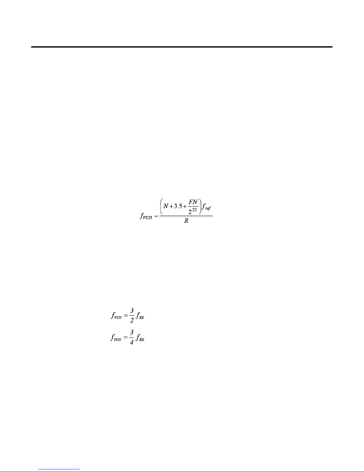
The generated frequency is given by the following equation:
where: fvco = Generated VCO frequency
N = N-divider ratio, integer part
FN = Fractional setting
R = R-divider ratio
fref = Reference frequency
A. UHF VCO Frequency Setting
To tune the receiver’s receive frequency (fRX), the VCO frequency (fVCO) is set according to the following
equations:
GSM850/EGSM900:
DCS1800/PCS1900:
B. Digital Frequency Centering
The SKY74400 re-centers the UHF VCO frequency range each time the synthesizer is programmed. This
proprietary Skyworks technique, called Digital Frequency Centering (DFC) extends the VCO frequency
coverage, speeds up settling time, and ensures robust performance since the VCO is always operated at
the center of its tuning range. Each time the synthesizer is programmed, the DFC circuit is activated and the
VCO is centered to the programmed frequency in less than 20 µs. After this, normal Phase Locked Loop
(PLL) operation is resumed and the fine settling of the frequency is finalized. DFC typically adjusts the VCO
center frequency to within a few MHz and no more than 5 MHz offset, and presets the tuning voltage to the
center of the range before the PLL takes over.

3. TECHNICAL BRIEF
- 19 -
This speeds up frequency settling and ensures that the PLL control voltage never operates close to the
rails. DFC is the result of an adaptive circuit that corrects for any VCO center frequency errors caused by
variations of the integrated VCO circuit such as temperature, supply voltage, or aging. The VCO can be
centered at any frequency in the range from 990 MHz to 1550 MHz. Once centered, the VCO has a
minimum analog tuning range of 20 MHz. No calibration or data storage is needed for DFC operation. It is
activated by one of two events:
• When the synthesizer is programmed, the rising edge of the LE signal starts the DFC cycle
• When the SXENA signal level is changed from low to high, which enables the synthesizer, the rising edge
of the SXENA signal starts the DFC cycle.
C. Integrated Loop Filters
Both loop filters (for the UHF PLL and for the transmit PLL) are fully integrated. Several adjustments can be
made to the loop filter transfer functions. The UHF loop filter has two synchronized charge pumps. The
frequency of the “zero“ factor (z1) in the PLL phase transfer function can be adjusted by varying the charge
pump currents, and the values of the internal R3 resistor and C3 capacitor.
Charge Pump Current Compensation for Constant PLL Bandwidth The VCOs in the SKY74400 use
Skyworks DFC technique. The nature of the DFC circuit increases the VCO control sensitivity (KVCO) as
the VCO frequency is increased. Without any compensation, this leads to an increase in the PLL loop gain
and an increased loop bandwidth for higher frequencies. In a classical PLL design, KVCO is typically
regarded as a constant. In this case, the loop gain decreases with increased frequency as the division ratio
of the loop is increased proportionally to frequency. Since it is usually desirable to keep the loop bandwidth
constant over the frequency range of interest, the SKY74400 includes a circuit that compensates the charge
pump current to keep the overall loop gain constant.
Charge pump current compensation for the UHF PLL can be programmed to one of three settings (nominal,
high, or low) or the charge pump current can be programmed to a constant value without compensation.
Refer to the Skyworks Programming Guide SKY74117 RF Transceiver for Standalone Devices or
Embedded MCMs for details.
D. Crystal Oscillator
A 26 MHz crystal oscillator provides the reference frequency for the synthesizer. the oscillator uses an
external 26 MHz crystal to generate an accurate oscillation frequency. The reference frequency can be
changed through coarse-tuning with an integrated capacitor array or fine-tuning with the integrated varactor
diode. The oscillator is coarse-tuned by switching in and out (using a digital word programmed with the
serial interface) the capacitor network (CAP_A and CAP_B) located at the input of the integrated buffer. The
oscillator is fine-tuned by providing a tuning voltage to the integrated varactor diode.
An output buffer is provided to drive the baseband circuitry. The frequency of the output is determined by
the FREQ_SEL signal. When this signal is connected to ground, the output is 13 MHz; when connected to
VCC or left floating, the output is 26 MHz. The oscillator core powers up when the SXENA signal is set to
logic 1.
3. TECHNICAL BRIEF
- 20 -
(3) Transmitter Part
To minimize the post-PA filtering requirements and any additional post-power amp losses, the transmit
path consists of a vector modulator and a frequency translation loop. The translation loop consists of
the following:
•
PFD and charge pump
•
In-loop modulator
•
One programmable divider
•
Integrated transmit loop filter
•
Two transmit VCOs and output buffers
A. Translation Loop
The translational loop includes a vector modulator and a frequency translation loop to minimize the post-PA
filtering requirements. the loop functions as a PLL with a mixer in the feedback path and a modulator in the
reference path. The loop provides a PFD and charge pump, integrated loop filters, two transmit VCOs,
down-conversion mixer in the feedback path, a frequency divider for frequency plan flexibility, and the
modulator. The mixers in the feedback path provide either high side or low side injection to provide flexibility
in the frequency plan. The modulator in the reference path uses a vector summing technique to reject the
unwanted image and to also sufficiently attenuate the 3rd and 5th harmonics. Therefore, no external IF
filters are required. The loop filter required for the transmit VCOs is integrated in the SKY74400.
B. Transmit VCOs
Two integrated transmit VCOs are designed to meet GSM850, EGSM900, DCS1800, and PCS1900
requirements. The transmit VCOs use the same DFC technique as the synthesizer section to lock the
translation loop. The rising edge on TXENA initializes the transmit DFC. The output buffers feed the signal
to the PAs. Two transmit buffers are provided, one for the low band VCO and the other for the high band
VCO.
Figure. 3-2 Crystal Oscillator BLOCK DIAGRAM

3. TECHNICAL BRIEF
- 21 -
C. Power Amplifier (PA)
The PA functionality of the SKY74400 consists of separate GSM850/EGSM900 and DCS1800/PCS1900
blocks, impedancematching circuitry for 50 output impedances, and a PAC block with an internal
currentsense resistor. The custom BiCMOS integrated circuit provides the internal PAC function and
interface circuitry. Fabricated onto a single Gallium Arsenide (GaAs) die, one Heterojunction Bipolar
Transistor (HBT) PA block supports the GSM850 and EGSM900 bands, and the other supports the
DCS1800 and PCS1900 bands. Both PA blocks share common power supply pins to distribute current. The
RF output ports of the SKY74400 are internally matched to a 50 load to reduce the number of external
components for a quad-band design. The PA also contains band-select switching circuitry to select GSM
(logic 0) or DCS/PCS (logic 1) as determined from the BAND_SELECT signal. The VBAT pin connects to an
internal current-sense resistor and interfaces to an iPAC function, which is insensitive to variations in
temperature, power supply, and process.
The ENABLE input allows initial power-on of PA circuitry to minimize battery drain.
(4) Low Drop-Out (LDO) Linear Voltage Regulators
The SKY74400 includes integrated LDO linear voltage regulators to eliminate the need for a separate
power management integrated circuit or discrete voltage regulators. Each functional block in the
SKY74400 includes a separate, internal LDO voltage regulator.
3. TECHNICAL BRIEF
- 22 -
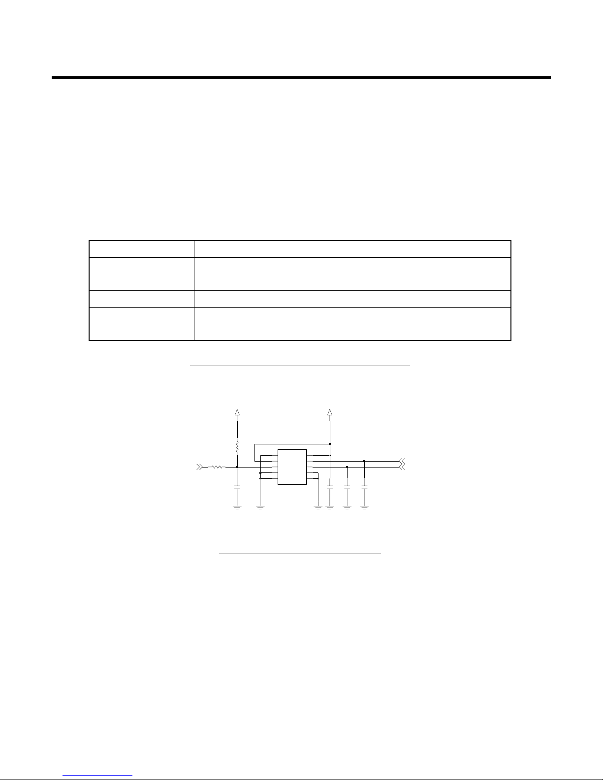
3.2 13 MHz Clock (VCTCXO, X501)
The 13 MHz clock(X501) consists of a TCXO(Temperature Compensated Crystal Oscillator) which
oscillates at a frequency of 13 MHz. It is used within the SKY74400, analog base band chipset (U101,
AD6535), digital base band chipset (U103, AD6527B).
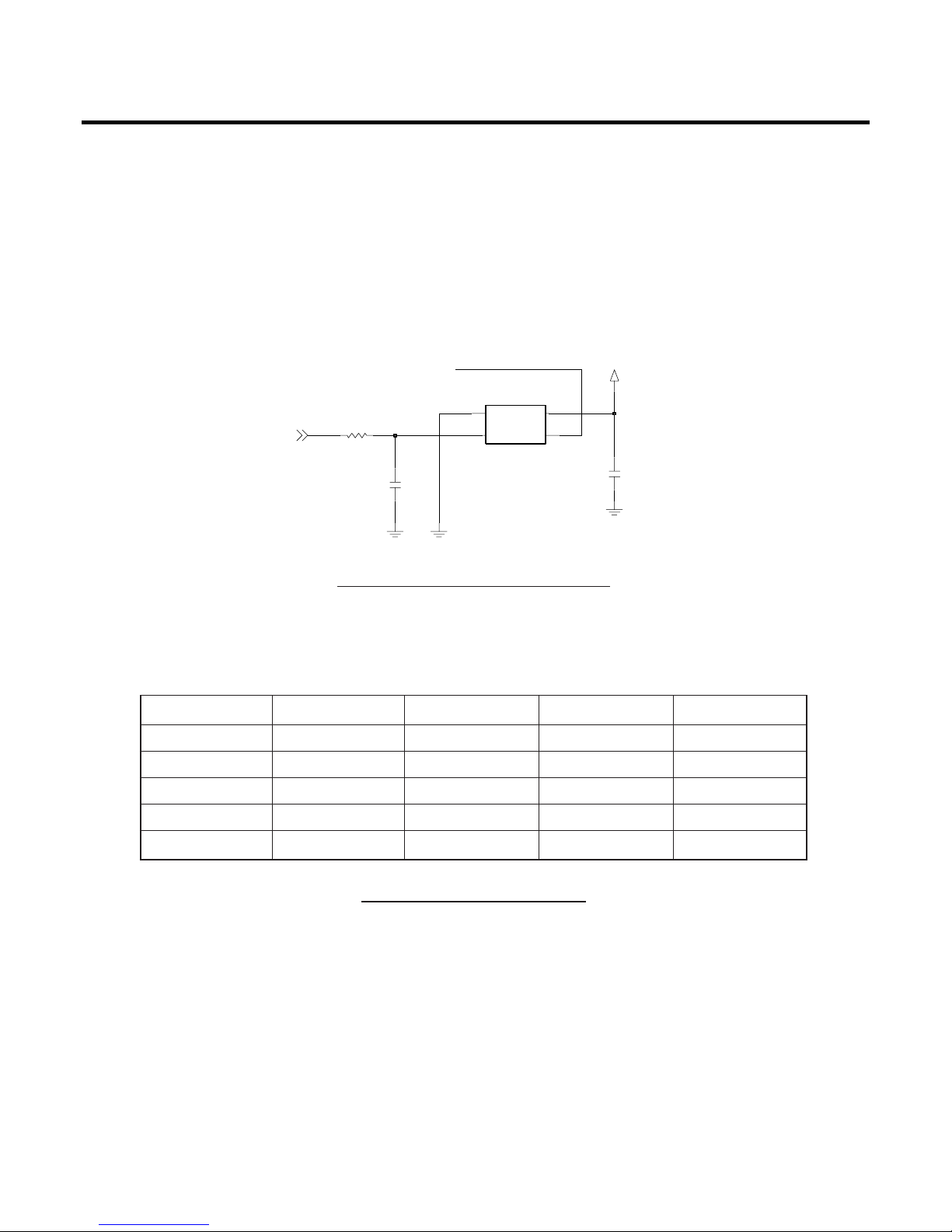
3.3 FEM for Triband(FL501)
(1608)
10KR507
2V75_VVCXO
C533
1000p
C532
2.2u
13MHz
X501
2
GND
3
OUT
4
VCC
1
VCONT
AFC
Figure 3-3 VCTCXO CIRCUIT DIAGRAM
Vc1 Vc2 Vc3 Current
EGSM-Tx 0.0-0.1V 0.0-0.1V 2.3-3.0V 10mA Max
EGSM-Rx 0.0-0.1V 0.0-0.1V 0.0-0.1V ≈ 0mA
DCS/PCS-Tx 0.0-0.1V 2.3-3.0V 0.0-0.1V 10mA Max
DCS-Rx 0.0-0.1V 0.0-0.1V 0.0-0.1V ≈ 0mA
PCS-Rx 2.3-3.0V 0.0-0.1V 0.0-0.1V 10mA Max
Table 3-1 FEM CONTROL LOGIC
3. TECHNICAL BRIEF
- 23 -
8
GSM1800_RX
4
GSM1900_RX
6
GSM900_RX
2
GSM900_TX
10
VC1
11
9
VC2
12
VC3
13
ANT
1
GND1
GND2
3
5
GND3
7
GND4
GND5
14
15
GND6
GND7
16
GSM18001900_TX
27p
LMSP54LA-445TEMP
FL501
C505
C507 27p
C506 27p
ANT_SW3
ANT_SW2
ANT_SW1
GSM900_TX
DCS_PCS_TX
Figure 3-4 FEM CIRCUIT DIAGRAM
3. TECHNICAL BRIEF
- 24 -
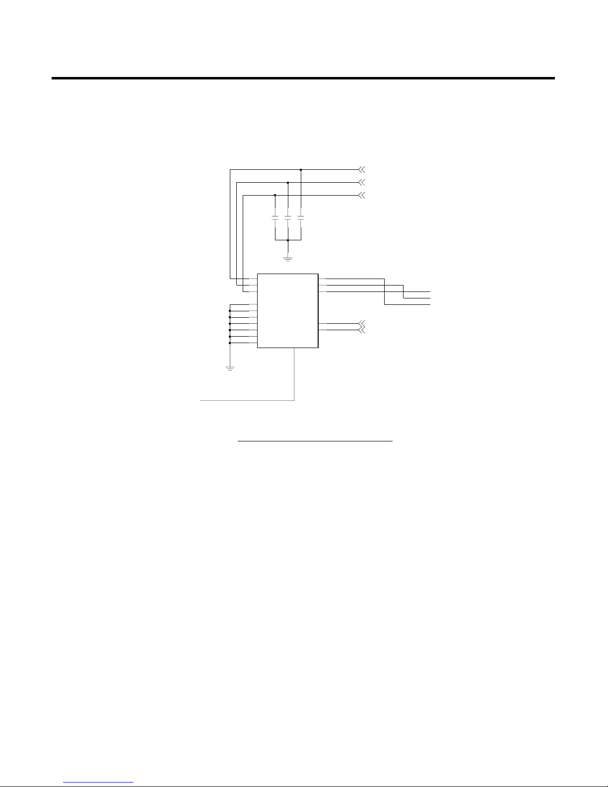
3.4 Digital Main Processor (AD6527B, U103)
Keypad
Matrix
Backlight/
Service Light
Flash
16-bit
SRAM
8 or 16 bit
(optional)
SIM
Application
Processor
USB Host
KEYPADCOL[7:0]
KEYPADROW[7:0]
Servicelight
BACKLIGHT[3.0]
USCTX/RX/CLK
ROMCS[1:0]
ADD[24:0]
DATA[15:0]
RAMCS[1:0]
RD
WR
HWR/UBS
LWR/LBS
DISPLAYCS[1:0]
Generic Serial
Port C
GPCS[1:0]
CLKIN
MicroSM
CSDO
CSFS
BSOFS
CSDI
BSDO
RF Interface
PA Supply
Enable
BSDI
BSIFS
ASDO
ASDI
ASFS
CLKOUT_GATE
CLKOUT
ABBRESET
PWRON
RESET
OSCIN
AD6527/AD6527B GSM-PROCESSOR
JTAGEN
TCK, TMS
TDI, TDO
JTAG
Power
Management
USC
32KHz
CSDI
CSFS
CSDO
BSDI
BSIFS
BSDO
BSOFS
ASDI
ASDO
ASFS
MCLK
RESET
VCXOEN
MCLKEN
DRV-OUT
LNA IN
RADIO
AD6534
AGC Synthesizer
VCO
13/
26MHz
JTAG
VOSC
AFC
RAMP
RF Timing
I/Q Interface
VOICE i/f &
Buzzer
Universal
System
Connector
(USC)
(Parallel)
JTAG, HSL, GPIO
Enhaoced Generic serial port A
Generic serial port B
Generic serial port D
SIM serial
Interface
SPI
USB Interface
*(AD6527B only)
OSCOUT
VDDRTC
VMEM
VEXT
VCC
VMMC
VINT
VDDUSB
VSIM
GND
ABB_INT
serial display
DISPLAY
Accessory
Devices
e.g
BATTERY
AUXCS[1:0]
Generic Serial Port D-A
Generic Serial Port D-B
GPIO[ ] / IRQ
INT
AD6535 Audio & Base band
Processor
Audio
Data
Port
BASE
BAND
I/Q
Serial
Port
control
serial
port
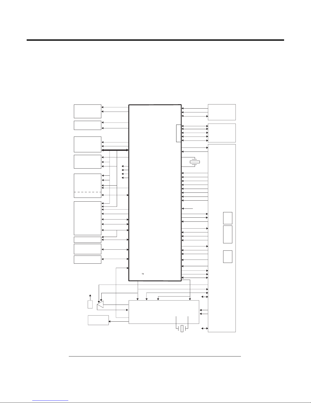
Figure 3-5. SYSTEM INTERCONECTION OF AD6527 EXTERNAL INTERFACE

3. TECHNICAL BRIEF
- 25 -
• AD6527 is an ADI designed processor.
• AD6527 consists of
1. Control Processor Subsystem
• 32-bit ARM7TDMI Control Processor
• 58.5 MHz operation at 1.7V
• On-board 16KB instruction/Data Cache
• 1 Mbits of on-chip System SRAM
2. DSP Subsystem
• 16-bit Fixed Point DSP Processor
• 91 MIPS at 1.7V
• 16K word Data and 16K word Program SRAM
• 4K word Program Instruction Cache
• Architecture supports Full Rate, Enhanced Full Rate, Half Rate, and AMR Speech
Encoding/Decoding Algorithms
3. Peripheral Subsystem
• Shared on-chip peripheral and off-chip interface:
• Support for Burst and Page Mode Flash
• Support for Pseudo SRAM
• Ciphering module for GPRS supporting GAE1 and GAE2 encryption algorithms
• Parallel and Serial Display Interface
• 8 x 8 Keypad Interface
• Four independent programmable backlight plus One Service Light
• 1.8V and 3.0V, 64 kbps SIM interface
• Universal System Connector Interface
• Slow, Medium and Fast IrDA transceiver interface
• Enhanced Generic Serial Port
• Dedicated SPI interface
• Thumbwheel Interface
• JTAG Interface for Test and In-Circuit Emulation
4. Other
• Supports 13 MHz and 26 MHz Input Clocks
• 1.8V Typical Core Operating Voltages
• 204-Ball LFBGA(mini-BGA) Package
5. Applications
• GSM900/DCS1800/PCS1900/PCS850 Wireless Terminals
• GSM Phase 2+ Compliant
• GPRS Class 12 Compliant
• Multimedia Services(MMS)
• Extended Messaging System(EMS)
3. TECHNICAL BRIEF
- 26 -
3.4.1 Interconnection with external devices
A. RTC block interface
Countered by external X-TAL
The X-TAL oscillates 32.768KHz
B. LCD module interface
The LCD module is controlled by AD6527B(U103),DBB.
In operating mode, the AD6527B(U103) controls the LCD module through _LCD_CS,
LCD_DIM_CTRL, LCD_RESET, LCD_WR, LCD_CS, 2V8_MV, IF_MODE.
Signals Description
_LCD_CS MAIN LCD driver chip enable. MAIN LCD driver IC has own CS pin
LCD_DIM_CTRL It controls dimming mode of LCD module.
LCD_RESET
This pin resets LCD module. This signal comes from DBB directly.
(GPIO 15)
_WR Enable writing to LCD Driver.
2V8_MV 2.8V voltage is supplied to LCD driver IC.
Table 3-2. LCD CONTROL SIGNALS DESCRIPTION
3. TECHNICAL BRIEF
- 27 -
The backlight of LCD module is controlled by DBB via AAT2807AIXN-4.5, U802. The control signals
related to Backlight LED are given bellow.
C. RF interface
The AD6527B control RF parts through PA_BAND, ANT_SW1, ANT_SW2, ANT_SW3 , CLKON ,
PA_EN, S_EN, S_DATA, S_CLK, RF_PWR_DWN.
Signals Description
LCD_DIM_CTL
Control LCD backlight level in 16 steps
(GPO 23)
LCD_LED_CTL Control LCD LED
LCD_LED_GND
Table 3-3. DESCRIPTION OF LCD BACKLIGHT LED CONTROL
Signals Description
PA_BAND (GPO 17) PAM Band Select
ANT_SW1 (GPO 9) Antenna switch Band Select
ANT_SW2 (GPO 11) Antenna switch Band Select
ANT_SW3 (GPO 10) Antenna switch Band Select
CLKON RF LDO Enable/Disable
PA_EN (GPO 16) PAM Enable/Disable
S_EN (GPO 19) PLL Enable/Disable
S_DATA (GPO 20) Serial Data to PLL
S_CLK (GPO 21) Clock to PLL
RF_PWR_DWN(GPO 4) Power down Input
Table 3-4. RF CONTROL SIGNALS DESCRIPTION
3. TECHNICAL BRIEF
- 28 -
D. SIM interface
The AD6527B provides SIM Interface Module. The AD6527 checks status periodically during
established call mode whether SIM card is inserted or not, but it doesn't check during deep Sleep
mode. In order to communicate with SIM card, 3 signals SIM_DATA, SIM_CLK,
SIM_RST(GPIO_23) are required. The descriptions about the signals are given by bellow Table 3-6
in detail.
E. Key interface
Include 5 column, 5 row. The AD6527B detects whether key is pressed or not by using interrupt
method.
F. AD6535 Interrupt
AD6535 provides an active-high interrupt output signal. Interrupt signals are generated by the
Auxiliary ADC, audio, and charger modules.
Signals Description
SIM_DATA
This pin receives and sends data to SIM card.
This model can support only 3.0 volt interface SIM card.
SIM_CLK Clock 3.25MHz frequency.
SIM_RST
Reset SIM block
(GPIO_23)
Table 3-5. SIM CONTROL SIGNALS DESCRIPTION
2V85_VSIM
27p
C322
GND5
10
IO
6
RST
2
1
VCC
5
VPP
J301
3
CLK
GND1
4
7
GND2
GND3
89
GND4
0R362
C323
1000p
20K
R361
220n
C320
2V85_VSIM
C321
NA
SIM_RST
SIM_CLK
SIM_DATA
Figure 3-6. SIM Interface of AD6527B
3. TECHNICAL BRIEF
- 29 -
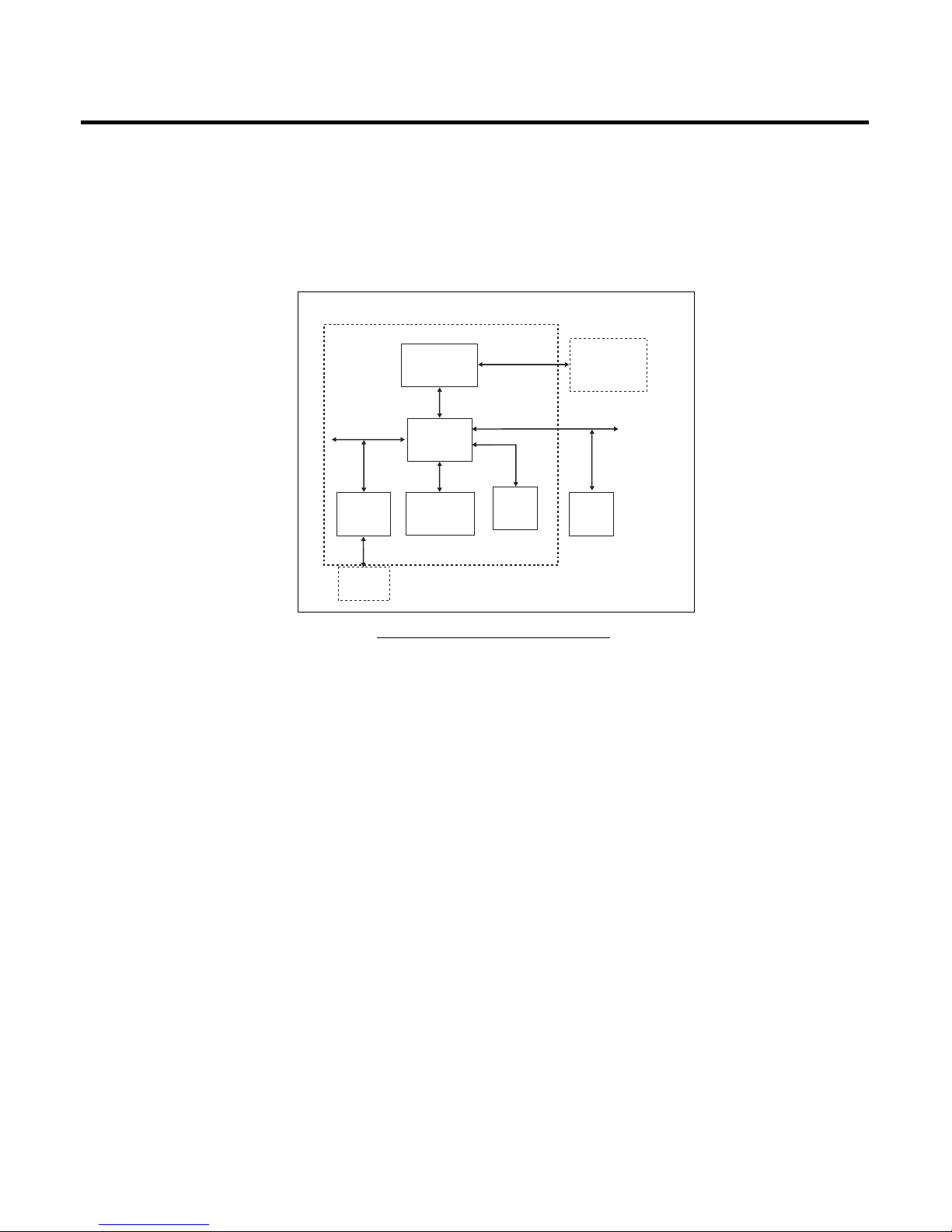
3.4.2 AD6527B Architecture
The internal architecture of AD6527B is shown above Figure 3-7. AD6527 regroups three main subsystems
connected together through a dynamic and flexible communication bus network. It also includes onboard
system RAM (SRAM) and interfaces with external Flash Memory, Baseband converter functions, and
terminal functions like MMI, SIM and Universal System Connector (USC).
The Digital Signal Processing (DSP) subsystem primarily hosts all the speech processing, channel
equalization and channel codec functions. The code used to implement such functions can be stored in
external Flash Memory and dynamically downloaded on demand into the DSP’s program RAM and
Instruction Cache.
The micro-controller subsystem supports all the GSM terminal software, including the layer 1, 2 and 3 of the
GSM protocol stack, the MMI, and applications software such as data services, test and maintenance. It is
tightly associated with on-chip system SRAM and also includes boot ROM memory with a small dedicated
routine to facilitate the initialization of the external Flash Memory via code download using the on-chip serial
interface to the external Flash Memory interface.
The peripheral subsystem is composed of system peripherals such as interrupt controller, real time clock,
watch dog timer, power management and a timing and control module. It also includes peripheral interfaces
to the terminal functions: keyboard, battery supervision, radio and display. Both the DSP and the MCU can
access the peripheral subsystem via the peripheral bus (PBUS).
For program and data storage, both the MCU subsystem and the DSP subsystem can access the on chip
system SRAM and external memory such Flash Memory. The access to the SRAM module is made through
the RAM Bus (RBUS) under the control of the bus arbitration logic. Similarly, access to the Flash Memory is
through the parallel External Bus (EBUS).
Figure 3-7. AD6527B Architecture
AD6527/AD6527B
AD6535
Audio Baseband
and Power
Management
DSP
SRAM
FLASH
MMI
USC
Peripheral
RF-Control
Subsystem
Subsystem
Subsystem
(ARM7TDMI
®
)
DMA and BUS
ARBITRATION
Serial Link
DSP BUS
RBUS IM
EBUS
PBUS
SBUS
MUC
3. TECHNICAL BRIEF
- 30 -
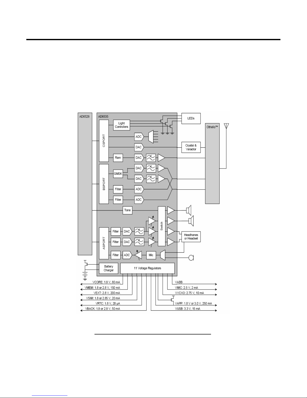
3.5 Analog Main & Power Management Processor
(AD6535, U101)
Figure 3-8. AD6535 FUNCTIONAL BLOCK DIAGRAM

3. TECHNICAL BRIEF
- 31 -
• AD6535 is an ADI designed Analog Baseband processor. AD6535 covers the processing GMSK
modulation interface, Aux ADC, Voice signal processing and Power Management.
• AD6535 consists of
1. BB Transmit section
• GMSK Modulation
• I-channel & Q-channel Transmit DACs and Filters
• Power Ramping DAC
2. BB Receive section
• I-channel & Q-channel Receive ADCs and Filters
3. Auxiliary section
• Voltage Reference
• Automatic Frequency Control DAC
• Auxiliary ADC
• Light Controllers
4. Audio Section
• 8 kHz & 16 kHz Voiceband Codec
• 48 kHz Monophonic DAC
• Power Amplifiers
5. Power Management section
• Voltage Regulators
• Battery Charger
• Battery Protection
6. Digital Processor section
• Control, Baseband, and Audio Serial Ports
• Interrupt Logic
 Loading...