

LG LS670 Service Manual
APCPCWM_4828539:WP_0000001WP_0000001
APCPCWM_4828539:WP_0000001WP_0000001
Table Of Contents
1. Introduction ..................................................2
1.1 Purpose .........................................................................................2
1.2 Regulatory Information ..........................................................2
Product Requirement Spec. ...........................4
1. Product Name ………………………………………………….………...6
2. Supporting Standard ………………………………………….……...6
3. Functions of Major Semi-Conductor ………………………..6
4. HW Feature ………………………………………………………………..7
5. SW Feature …………………………………………………………………8
6. LS670 Figure …………………………………………………………….10
2. Product Specification ……………………….11
2.1 LG-LS670 Main Feature …………………………………………11
2.2 LG-LS670 Main Component ………………………………….12
3. Technical Brief Description ………………15
3.1 Digital Basband(DBB/MSM7627) …………………………...15
3.2 Hardware Architecture …………………………………………...16
3.3 Memory Support Feature ………………….…………………...21
3.4 Power Block ………………………………………….………………...22
3.5 HW Sub System …………………………………….….…………….27
3.6 Audio and sound ……………………………………………………30
3.7 Display ……………………………………………………………………..35
3.8 Proximity Sensor …………………………………………………….36
3.9 Motion Sensor ………………………………………………………..36
3.10 Vibrator ……………………………………………………….………..37
3.11 CDMA RF Transmit/Receive Part ………………….……..38
5. Block Diagram …………………………………….149
6. Circuit Diagram …………………………………...158
7. PCB Layout ………………………..……………….167
8. BGA Pin Map …………………………….………..170
8.1 MSM7627 …………………..............................…………………………..170
8.2 PM7540 ………………………………………………………………………..171
8.3 MCP ……………………………………………………………………………...172
9. Calibration & RF Auto Test Program
(Tachyon) …………………………..………..173
10. Exploded view …………………………………….179
11. Components List ………………………………...181
4. Trouble Shooting ……………………………..44
4.1 CDMA Rx Part Trouble …………………………………..……….44
4.2 CDMA Tx Part Trouble ……………………………………………70
4.3 Power Trouble ……………………………………………………….114
4.4 Audio Trouble ………………………………………………………..123
4.5 3M Camera Trouble ………………………………………………133
4.6 Main LCD Trouble ……………………………………..………….135
4.7 Key Trouble ……………..…………………………………………….137
4.8 Vibrator Trouble …………..…………………………..…………140
4.9 Proximity Sensor on/off Trouble …………………..……...142
4.10 Motion Sensor on/off Trouble ………………..…………..143
4.11 Compass Sensor on/off Trouble ………………………...145
4.12 Touch Sensor Trouble ………………………………………...148
APCPCWM_4828539:WP_0000001WP_0000001
APCPCWM_4828539:WP_0000001WP_0000001
LS670
1. Introduction
1.1. Purpose
This manual provides the information necessary to repair, calibration, description and download the
features of this model.
1.2. Regulatory Information
A. Security
Toll fraud, the unauthorized use of telecommunications system by an unauthorized part (for example,
persons other than your company’s employees, agents, subcontractors, or person working on your
company’s behalf) can result in substantial additional charges for your telecommunications services.
System users are responsible for the security of own system.
There are may be risks of toll fraud associated with your telecommunications system. System users
are responsible for programming and configuring the equipment to prevent unauthorized use. The
manufacturer does not warrant that this product is immune from the above case but will prevent
unauthorized use of common carrier telecommunication service of facilities accessed through or
connected to it. The manufacturer will not be responsible for any charges that result from such
unauthorized use.
B. Incidence of Harm
If a telephone company determines that the equipment provided to customer is faulty and possibly
causing harm or interruption in service to the telephone network, it should disconnect telephone
service until repair can be done. A telephone company may temporarily disconnect service as long as
repair is not done.
C. Changes in Service
A local telephone company may make changes in its communications facilities or procedure. If these
changes could reasonably be expected to affect the use of the phones or compatibility with the net
work, the telephone company is required to give advanced written notice to the user, allowing the user
to take appropriate steps to maintain telephone service.
D. Maintenance Limitations
Maintenance limitations on the phones must be performed only by the manufacturer or its authorized
agent. The user may not make any changes and/or repairs expect as specifically noted in this manual.
Therefore, note that unauthorized alternations or repair may affect the regulatory status of the system
and may void any remaining warranty.
E. Notice of Radiated Emissions
This model complies with rules regarding radiation and radio frequency emission as defined by local
regulatory agencies. In accordance with these agencies, you may be required to provide information
such as the following to the end user.
F. Pictures
The pictures in this manual are for illustrative purposes only; your actual hardware may look slightly
different.
G. Interference and Attenuation
2
APCPCWM_4828539:WP_0000001WP_0000001
APCPCWM_4828539:WP_0000001WP_0000001
LS670
A phone may interfere with sensitive laboratory equipment, medical equipment, etc. Interference from
unsuppressed engines or electric motors may cause problems.
H. Electrostatic Sensitive Devices
ATTENTION
Boards, which contain Electrostatic Sensitive Device (ESD), are indicated by the sign. Following
information is ESD handling:
• Service personnel should ground themselves by using a wrist strap when exchange system boards.
• When repairs are made to a system board, they should spread the floor with anti-static mat which is
also grounded.
• Use a suitable, grounded soldering iron.
• Keep sensitive parts in these protective packages until these are used.
• When returning system boards or parts like EEPROM to the factory, use the protective package as
described.
3
APCPCWM_4828539:WP_0000001WP_0000001
APCPCWM_4828539:WP_0000001WP_0000001
LS670 Product SPEC
LS670
Product Requirement SPEC.
October, 15, 2010
(RevA.0)
LG Electronics Inc.
4

APCPCWM_4828539:WP_0000001WP_0000001
APCPCWM_4828539:WP_0000001WP_0000001
LS670 Product SPEC
− Contents −
1. Product Name ……………………………………………………………6
2. Supporting Standard …………………………………………………..6
3. Main Parts ………………………………………………………………….6
4. H/W Features ………………………………………………………………7
5. S/W Features …………………………………………………………….. 8
6. LS670 Figures …………………………………………………………... 10
5
APCPCWM_4828539:WP_0000001WP_0000001
APCPCWM_4828539:WP_0000001WP_0000001
LS670 Product SPEC
1. Product Name
LS670 : US Cellular/US PCS + GPS
(EVDO Rev_0 / EVDO Rev_A)
2. Supporting Standard
Item Feature Comment
Supporting
Standard
US Cellular / US PCS/GPS
Frequency Range US Cellular TX : 824.82 ~ 848.19 MHz
US Cellular RX : 869.82~893.19 MHz
US PCS TX : 1850~1910 MHz
US PCS RX : 1930~1990 MHz
GPS : 1575.42 MHz
3. Functions of Major Semi-Conductors
Classification Function
MSM7627 Terminal operation control and digital signal processing
Memory
(MT29C4G96MAZAPCJA-5IT)
NAND Flash Memory (4G) + SDRAM (4G)
Storing of terminal operation program
RTR6500 Converts Rx and Tx RF signal to baseband signal
6
APCPCWM_4828539:WP_0000001WP_0000001
APCPCWM_4828539:WP_0000001WP_0000001
LS670 Product SPEC
4. HW Features
Item Feature Comment
Form Factor DOP
Battery
1) Capacity
Standard : Li-Ion, 1500mAh
2) Packing Type : Soft Pack
Size Standard : 113.5 x 59 x 13.3(mm)
Weight 133g
Volume TBD
PCB 3-8 Staggered 10 Layers , 0.8t
Stand by time CDMA DCN/PCS over 168 hrs @ SCI=2(pwr: -75dBm)
Charging time Up to 300 min @ Power Off/ 1500mAh
Talk time CDMA over 180mins @ Rx pwr -92dBm
LCD 3.2” HVGA (480x320 pixel) 16M TFT
LCD
Built-in Camera 3.2Mega Auto Focus 3.2M AF
Keypad Function Key : 4
Side Key : 5
ANT Main : Internal Fixed Type
MRD : Internal Fixed Type
System connector 5 Pin
Ear Phone Jack
4pole, 3.5Φ Ear Jack
Memory NAND Flash : 4Gbit
SDRAM : 4Gbit
Speech coding EVRC, QCELP, AMR
Data & Fax Built in Data support
Vibrator Built in Vibrator
Blue Tooth V2.1 + EDR
MIDI(for Buzzer
SW decoded
Function)
Music Player MP3, AAC, AAC+, WMA, OGG
Video Player H.263, H.264, MPEG-4, WMV
Camcorder MPEG-4
Function Key: Back,
Search, Home, Menu
Side Key : PWR, CAM,
Google VOICE,
Volume up/down
Voice Recording Yes
Speaker Phone mode
Yes
Support
Trave l A dap te r Yes
CDROM No
Stereo Headset No
Data Cable Yes
T-Flash
Yes
(External Memory)
7
APCPCWM_4828539:WP_0000001WP_0000001
APCPCWM_4828539:WP_0000001WP_0000001
LS670 Product SPEC
5. SW Features
Item Feature Comment
RSSI Yes
Battery Charging Yes
Key Volume Yes
Audio Volume Yes
Time / Date Display Yes
Multi-Language Yes English, Spanish, Korean,
Chinese
Quick Access Mode Camera
PC Sync No
Speed Dial No
Profile No
CLIP / CLIR No
Phone Book Given Name/Family Name/
Phone:
Home/Mobile/Work/Work
Fax/Home
Fax/Pager/other/Custom
Email:
Home/Work/Other/Custom
IM:
AIM/Windows
Live/Yahoo/Skype/QQ/Google
Talk/ICQ/Jabber/Custom
Postal address:
Home/Work/Other/Custom
Organization:
Work/Other/Custom
Notes
Nickname
Website
Last Dial Number Yes Last Dial Numbers, Last
Last Received
Yes Last Dial Numbers, Last
Number
Last Missed Number Yes Last Dial Numbers, Last
Search by Number
Name
/ Name
Group Yes There is no limitation on the
There is no limitation on the
number of items.
It depends on Available memory
amount.
Received Numbers and Last
Missed Numbers can store.
Received Numbers and Last
Missed Numbers can store .
Received Numbers and Last
Missed Numbers can store.
number of items.
It depends on
available memory amount.
Group features can not be added
or edited by user.
8
APCPCWM_4828539:WP_0000001WP_0000001
APCPCWM_4828539:WP_0000001WP_0000001
LS670 Product SPEC
Fixed Dial Number No
Service Dial Number No
Own Number No
Voice Memo No Voice Recording is available but
there isn't relevant application in
initial status of this phone.(User
can download it)
Call Reminder No
Network Selection Automatic /Manual
Mute Yes
Call Divert No
Call Barring No
Call Charge (AoC) No
Call Duration No
SMS (EMS) There is no limitation on the
number of items.
It depends on available
memory amount.
SMS Over GPRS No
EMS Melody / Picture
Send / Receive / Save
MMS MPEG4
Send / Receive / Save
No
No
Yes
Yes
Long Message Yes
Cell Broadcast No
Download FUMO / GOTA
Game No
Calendar Yes
Memo No
World Clock No
Unit Convert No
Stop Watch No
Wall Paper Yes
WAP Browser No Support HTML Browser
Download Melody /
Yes Android Market
Wallpaper
SIM Lock No
SIM Toolkit No
MMS Yes
EONS No
CPHS No
Camera Yes 3.2M AF
JAVA No
Voice Dial Yes
IrDa No
Bluetooth Yes Ver. 2.1+EDR
FM radio No
EMS does not support.
(HSP,HFP,A2DP,AVRCP,OPP,FTP)
Hold / Retrieve Yes
Conference Call Yes Max. 3
9
APCPCWM_4828539:WP_0000001WP_0000001
APCPCWM_4828539:WP_0000001WP_0000001
LS670 Product SPEC
DTMF Yes
Memo pad No
TTY Yes
AMR Yes
SyncML No
IM Yes Google Talk
Email Yes
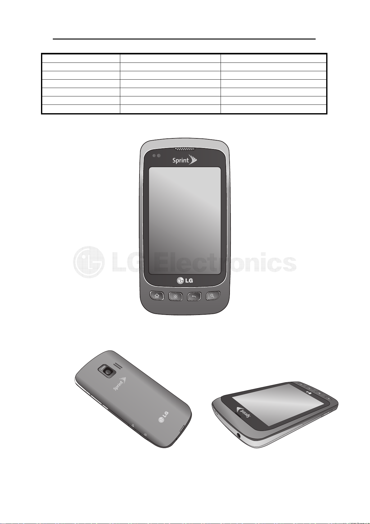
6. LS670 Figures
10
APCPCWM_4828539:WP_0000001WP_0000001
APCPCWM_4828539:WP_0000001WP_0000001
2. Product Specification
2. Product Specification
2.1. LG-LS670 Main Features
■ DOP type
■ Main Chipset : MSM7627, Memory (4Gbits NAND Flash + 4Gbits DDR SDRAM)
■ Display : 3.2”, 480 x 320 pixels, 16M Colors, TFT
■ CMX 4.0 compliant(72 Poly)
■ OS : Android 2.2 Froyo
■ Camera : Built-in Camera (3.2M AF pixels, CMOS Image sensor)
■ PMIC : Power control, Charger controller, Battery Voice Safety Recording/Memo/Playback,
Voice Recognition System
■ E911(gpsOne), TTY/TDD
■ Web Browser : Browser
■ 3D Graphics GUI : Menu, Animations, Flash UI
■ Support Micro-SD Card : External Memory
■ Bluetooth 2.1 EDR
■ WLAN 802.11 b/g
11

APCPCWM_4828539:WP_0000001WP_0000001
APCPCWM_4828539:WP_0000001WP_0000001
2. Product Specification
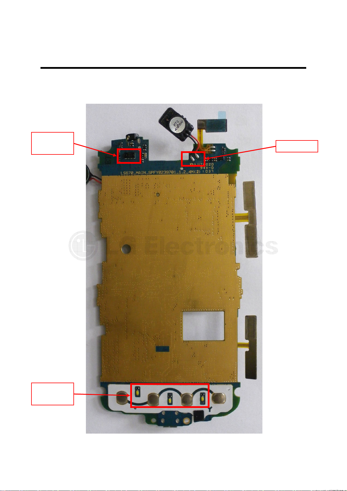
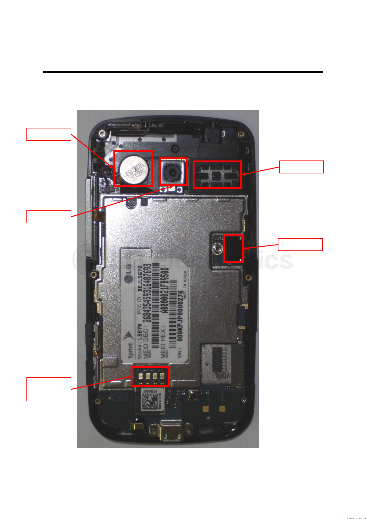
2.2 LG-LS670 Main Component
Ear Jack
CAMERA
Conn
TOUCH
Conn
MOTOR
Conn
RF Circuit
PMIC
3-AXIS
SENSOR
TCXO
Speaker
Audio
WIFI/BT
Memory
LCD Conn
MSM7627
Sub PMIC
Compass
CHARGING
CIRCUIT
MIC
RF Circuit
T-Flash
Socket
Micro USB
Main board, BOTTOM
12
APCPCWM_4828539:WP_0000001WP_0000001
APCPCWM_4828539:WP_0000001WP_0000001
Proximity
Sensor
2. Product Specification
Receiver
Keypad
LED
Main board, TOP
13
APCPCWM_4828539:WP_0000001WP_0000001
APCPCWM_4828539:WP_0000001WP_0000001
2. Product Specification
MOTOR
Speaker
Camera
Battery
Contact
LCD FPCB
Main board, Bottom
14
APCPCWM_4828539:WP_0000001WP_0000001
APCPCWM_4828539:WP_0000001WP_0000001
3. Technical Brief
3. Technical Brief Description
3.1 Digital Baseband(DBB/MSM7627)
3.1.1 General Description
A. Features(MSM7627)
15
APCPCWM_4828539:WP_0000001WP_0000001
APCPCWM_4828539:WP_0000001WP_0000001
3. Technical Brief
3.2 Hardware Architecture
<TOTAL Block>
Figure. Simplified Block Diagram
16
APCPCWM_4828539:WP_0000001WP_0000001
APCPCWM_4828539:WP_0000001WP_0000001
3. Technical Brief
<RF Block>
17
APCPCWM_4828539:WP_0000001WP_0000001
APCPCWM_4828539:WP_0000001WP_0000001
3. Technical Brief
<Power Block>
맑은 고딕
18
APCPCWM_4828539:WP_0000001WP_0000001
APCPCWM_4828539:WP_0000001WP_0000001
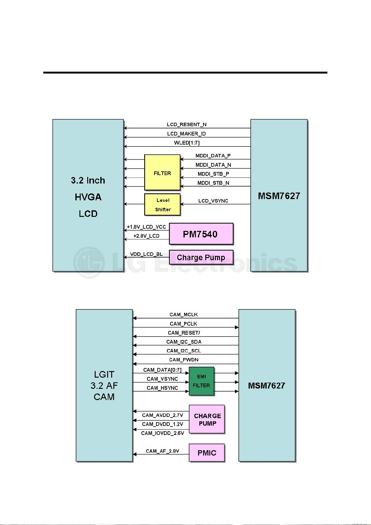
3. Technical Brief
<LCD Interface >
<CAMERA Interface >
19
APCPCWM_4828539:WP_0000001WP_0000001
APCPCWM_4828539:WP_0000001WP_0000001
3. Technical Brief
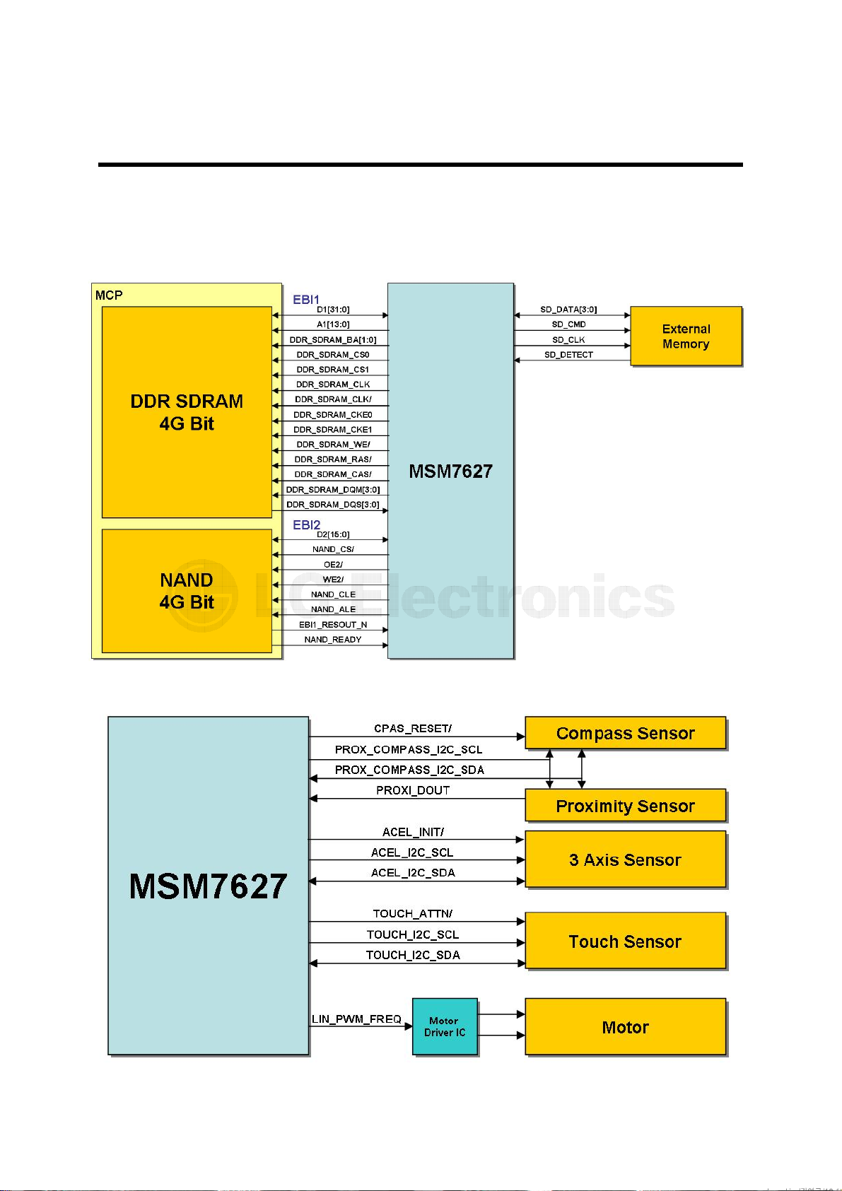
<External Memory >
<SENSOR & MOTOR >
20
APCPCWM_4828539:WP_0000001WP_0000001
APCPCWM_4828539:WP_0000001WP_0000001
3. Technical Brief
3.2.1 Architecture and baseband processing features
3.3 Memory support features
21
APCPCWM_4828539:WP_0000001WP_0000001
APCPCWM_4828539:WP_0000001WP_0000001
3. Technical Brief
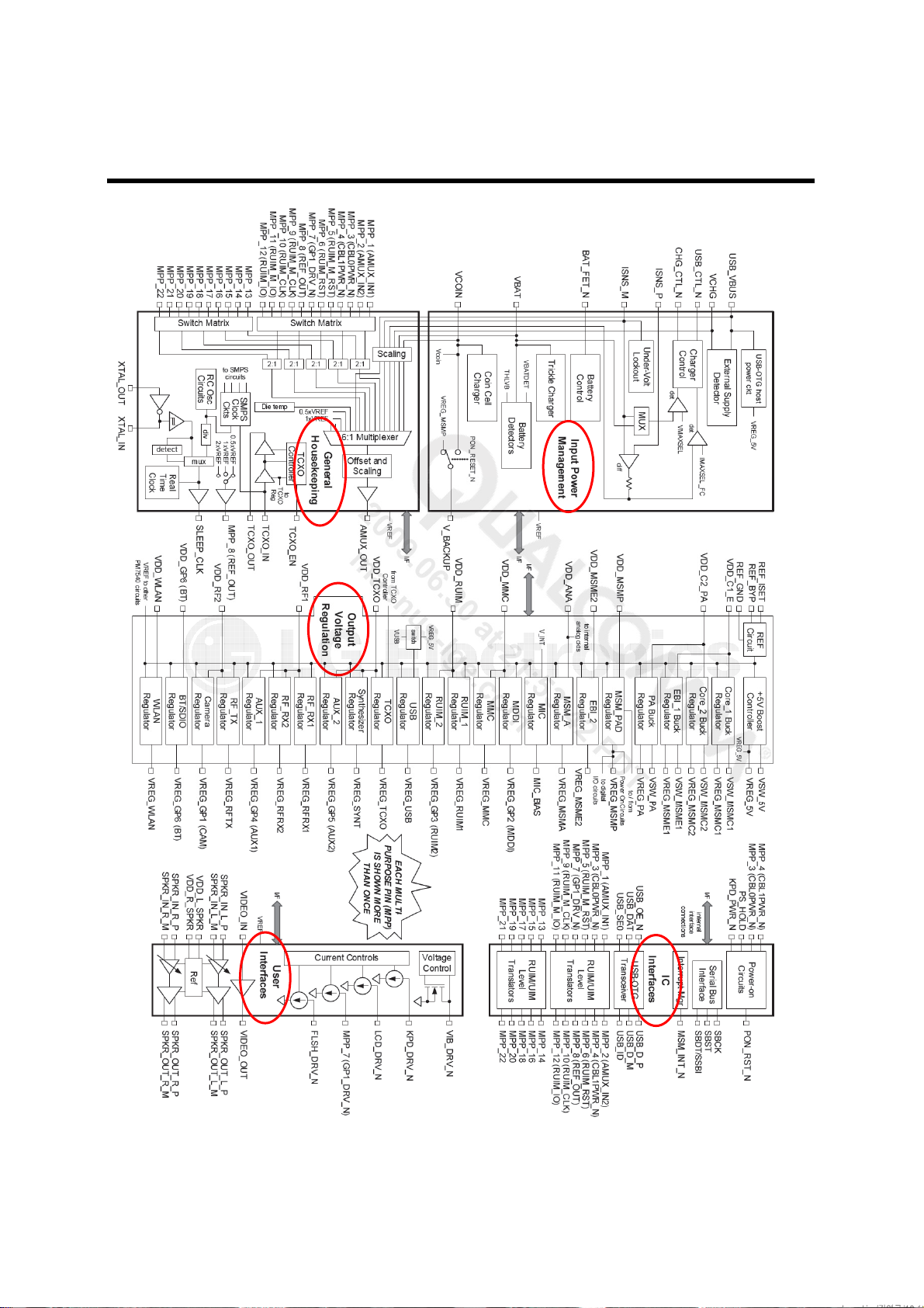
3.4. Power Block
3.4.1. General
MSM7627 is covered by PM7540(Qualcomm PMIC),
PM7540 cover the power of MSM7627, memory, RF block(RTR6500), and TCXO.
Major power components are :
PM7540(U405) : Phone main PMIC
AAT2862(U601) : LCD BLT Charge Pump
NUS5530MN(Q401) : main power path switch( battery charging circuit )
MAX14528(U401) : OVP( Over voltage protection) IC
3.4.2 PM7540
The PM7540 device (Figure) integrates all wireless handset power management. The power
management portion accepts power from all the most common sources – battery, external
charger, adapter, coin cell back-up – and generates all the regulated voltages needed to power
the appropriate handset electronics. It monitors and controls the power sources, detecting which
sources are applied, verifying that they are within acceptable operational limits, and coordinates
battery and coin cell recharging while maintaining the handset electronics supply voltages. Eight
programmable output voltages are generated using low dropout voltage regulators, all derived
from a common trimmed voltage reference.
A dedicated controller manages the TCXO warm-up and signal buffering, and key parameters
(under-voltage lockout and crystal oscillator signal presence) are monitored to protect against
detrimental conditions.
MSM7627 device controls and statuses the PM7540 IC using Single Serial Bus Interface (SSBI)
supplemented by an Interrupt Manager for time-critical information. Another dedicated IC
Interface circuit monitors multiple trigger events and controls the power-on sequence.
22
APCPCWM_4828539:WP_0000001WP_0000001
APCPCWM_4828539:WP_0000001WP_0000001
3. Technical Brief
Figure. PM7540 Functional Block Diagram
23
APCPCWM_4828539:WP_0000001WP_0000001
APCPCWM_4828539:WP_0000001WP_0000001
3. Technical Brief
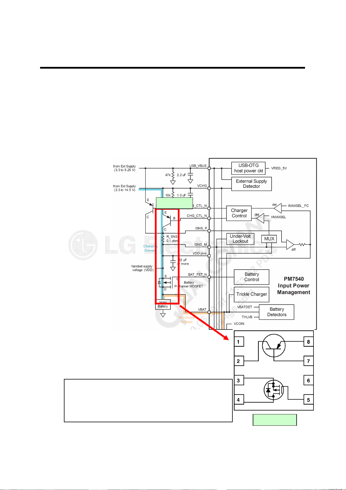
3.4.3. Charging control
A programmable charging block in PM7540 is used for battery charging. It is possible to set
limits for the charging current. The external supply typically connects directly to pin (VCHG). The
voltage on this pin (VCHG) is monitored by detection circuitry to ascertain whether a valid
external supply is applied or not. For additional accuracy or to capture variations over time, this
voltage is routed internally to the housekeeping ADC via the analog multiplexer. PM7540
circuits monitor voltages at VCHARGER and ICHARGE pins to determine which supply should be
used and when to switch between the two supplies. These pins are connected to the Source (or
emitter) and Drain (or collector) contacts of the pass transistor respectively.
1) Pass active transistor is “on” continuously closed-loop controlled
to regulate the total current
2) Battery transistor is turned on,
connecting battery to VDD node
3) Charging current (blue) flows
from the external supply
4) Total current is set by the current
regulation loop as described earlier
5) Battery voltage is routed to MSM
: MSM HKADC measures VBAT
6) Constant current charging is finished when
the battery reaches its target voltage
NUS5503MN
U8210 Charging Control block
PM7540 only include charging controller.
So it is necessary external charging path TR.
This is NUS5530MN.
This part also include battery side power path.
24
NU5530MN
APCPCWM_4828539:WP_0000001WP_0000001
APCPCWM_4828539:WP_0000001WP_0000001
3. Technical Brief
Constant Current Charging
The PM7540 IC supports constant current charging of the main battery by controlling the charger pass
transistor and the battery transistor. The constant current charging continues until the battery reaches its
target voltage, 4.2V.
Constant Voltage Charging
Constant voltage charging begins when the battery voltage reaches a target voltage, 4.2V.
The end of constant voltage charging is commonly detected 10% of the full charging
current.
• Charging Method : CC & CV (Constant Current & Constant Voltage)
• Maximum Charging Voltage : 4.2V
• Maximum Charging Current : 700mA
• Nominal Battery Capacity : 1500mAh
• Charging time : Max 5 Hours
• Full charge indication current (icon stop current) : 200mA
• Cut-off voltage : 3.40V
@ Battery icon display
100 ~ 90%
70% ~ 89%
50% ~ 69%
25
20% ~ 49%
15% ~ 19%
5% ~ 14%
0% ~ 4%

APCPCWM_4828539:WP_0000001WP_0000001
APCPCWM_4828539:WP_0000001WP_0000001
3. Technical Brief
Trickle Charging
Trickle Charging of the main battery, enabled through SBI control and powered from VDD, is
provided by the PM7540 IC, The trickle charger is on-chip programmable current source that
supplies current from V
nickel-based batteries, with its performance specified below (3.2V). The charging current is
set to 80mA.
to pin (VBAT). Trickle charging can be used for lithium-ion and
DD
UnitMaxTypMinParameter
PM7540
Input Power
Management
mA1008060Trickle Current
26
APCPCWM_4828539:WP_0000001WP_0000001
APCPCWM_4828539:WP_0000001WP_0000001
3. Technical Brief
3.5 H/W Sub system
3.5.1. HS-USB
The universal serial bus (USB) is an interconnection standard widely supported by the electronic
industry. The USB2.0 spec defines data rates as low-speed (1.5 Mbps), full-speed (12Mbps) and
hi-speed (480 Mbps). When two devices are connected via a USB interface, one of the devices
must act as a host, and the other device must act as a peripheral. The host is responsible for
initiating and controlling traffic on the bus. The USB specification requires personal computers
(PCs) to act as hosts, and other devices such as printers, keyboards, mice, etc. to act as
peripherals. The OTG supplement creates a new class of devices called OTG devices. OTG
devices can act as either hosts or peripherals, depending upon how they are connected and/or
used.
The MSM7627A device contains a new USB high-speed function that is based on a embedded
UTMI+ core with a UTMI+ low pin interface (ULPI) compatible port. The MSM device’s ULPI
interface connects to an external ULPI PHY chip to complete the design. The ULPI core
embedded in the MSM along with the PM7540 IC and a USB high-speed PHY IC provide support
for the high-speed interface.
Figure. USB block( MSM7627, MAX14528 )
27
APCPCWM_4828539:WP_0000001WP_0000001
APCPCWM_4828539:WP_0000001WP_0000001
3. Technical Brief
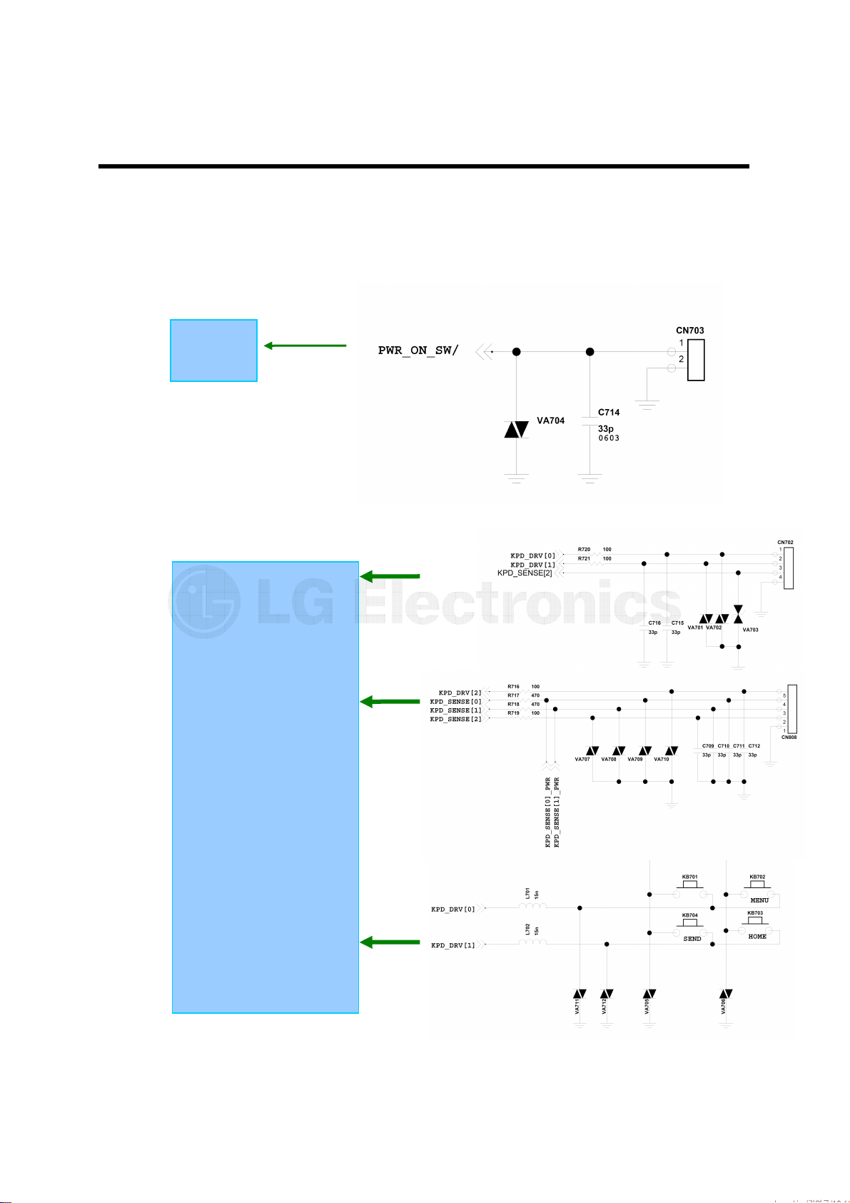
3.5.2. KEY
3.5.2.1 Power key
The power key is controlled by PM7540.
PM7540
3.5.2.2 key
The HOT Keys (Home, Menu, Search, Back) and the SIDE Keys (Volume, Camera, Google
Voice) are controlled by MS7627.
Volume Key
MSM7627
CAM Key
Figure. HOT KEY & SIDE KEY
28
HOT Key
APCPCWM_4828539:WP_0000001WP_0000001
APCPCWM_4828539:WP_0000001WP_0000001
3. Technical Brief
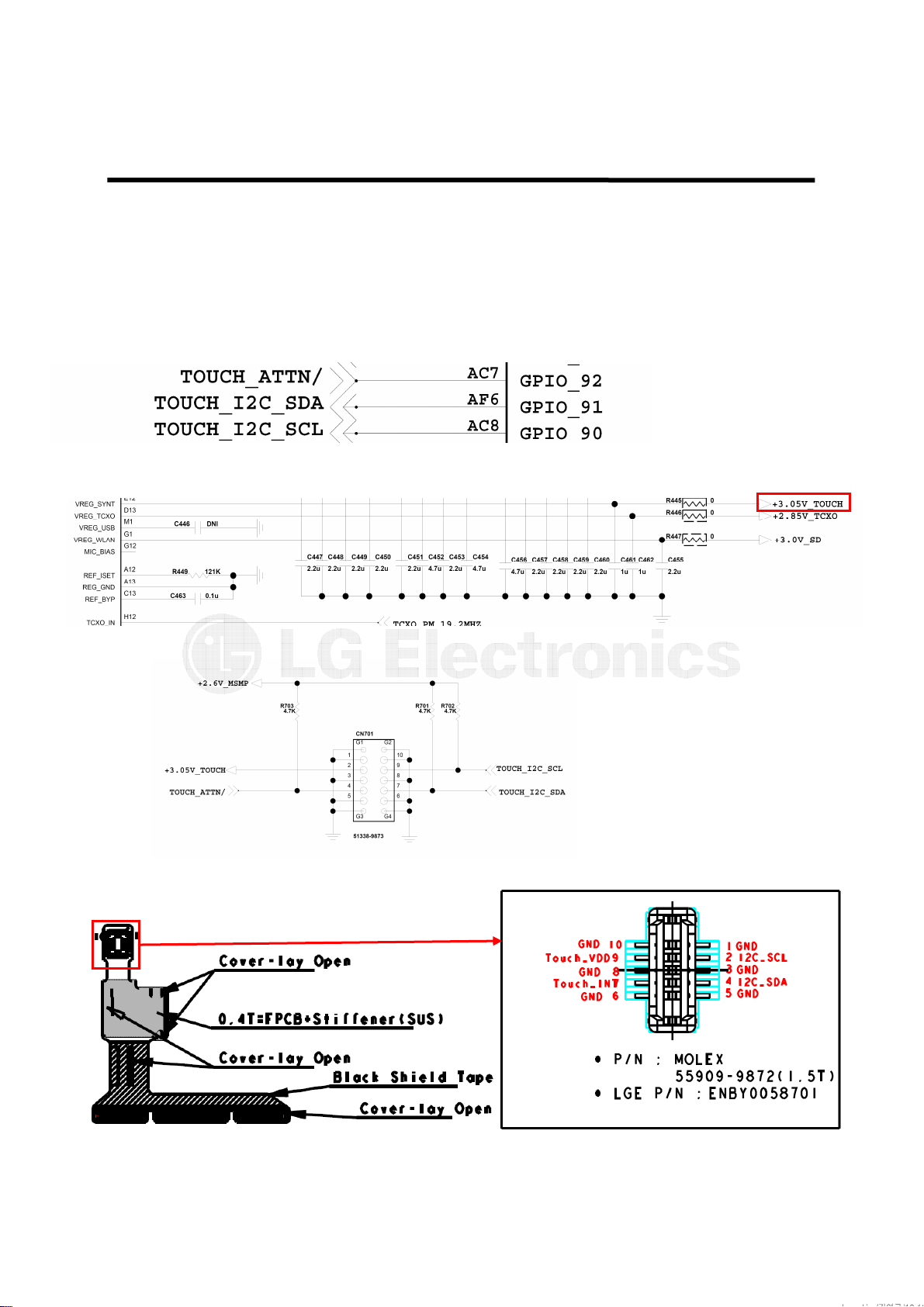
3.5.3.Touch Windows Interface
Touch screen is a capacitive sensor with an attached flexible PCB.
Touch pannel has 1-I2C line, 1-interrupt line, 1-power line.
<MSM7627 Direct Signal >
MSM7627
M
<PM7540 Direct Signal - Power>
P
7
5
4
0
< Main connector to Touch Window FPCB >
< Touch Sensor Module FPCB >
29
APCPCWM_4828539:WP_0000001WP_0000001
APCPCWM_4828539:WP_0000001WP_0000001
3. Technical Brief
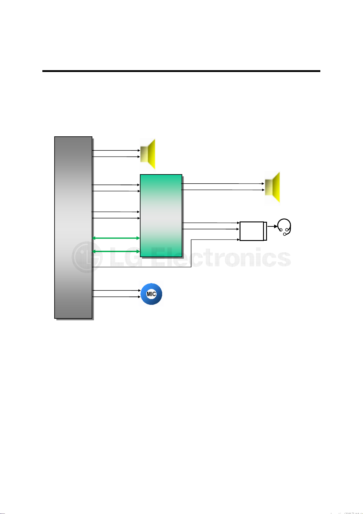
3.6. Audio and sound
3.6.1. Overview of Audio path
MSM7627
EAR10_P
EAR10_N
LINE_P
LINE_N
HPH_R
HPH_L
I2C_SCL
I2C_SDA
EAR_MIC+
MIC+
MIC_BIAS
Receiver
12X07
Audio Sub
System
WM9093
Earjack_R
Earjack_L
Speaker
18X10
Earjack
3.5ø
Figure. Block diagram of Audio path
30
 Loading...