

LG LMX430EMW Owner's Manual [es]

MOBILE PHONE
SERVICE MANUAL
CAUTION
BEFORE SERVICING THE UNIT, READ THE “SAFETY PRECAUTIONS” IN THIS MANUAL
MODEL : LM-X430EMW
Any reproduction, duplication, distribution (including by way of email, facsimile or other electronic means),
publication, modification, copying or transmission of this Service Manual is STRICTLY PROHIBITED unless you
have obtained the prior written consent of the LG Electronics entity from which you received this Service Manual.
The material covered by this prohibition includes, without limitation, any text, graphics or logos in this Service
Manual
Copyright ⓒ 2019 LG Electronics. Inc. All rights reserved.
Only training and service purposes
Date: September 2019 / Issue 1.0

Table Of Contents
1. INTRODUCTION.................................................2
1.1 Purpose
1.2 Regulatory Information
2. PERFORMANCE................................................... 3
2.1 Band Specification
2.2 HW Features
2.3 RSSI Display
2.4 Current consumption
2.5 Battery bar
2.6 SW Specification
3. TROUBLE SHOOTING..........................................11
3.1 Checking XO Block
3.2 Checking Transceiver DC Power Supply Circuit Block
3.3 Checking DC-DC Block
3.4 ASM Block
3.5 GSM, WCDMA, LTE PART
3.5.1 GSM, WCDMA, LTE PART - PRx
3.5.2 WCDMA, LTE PART – Tx
3.5.3 GSM PART – Tx
3.5.4 GSM,WCDMA, LTE PART - DRX
3.6 Power
3.7 Charger
3.8 Audio Block
3.8.1 Audio receiver
3.8.2 Audio speaker
3.8.3 Audio Main Mic
3.8.4 Audio sub Mic
3.8.5 Audio Ear mic jack
3.9 Checking LCD Block
3.10 Checking Touch Block
3.11 Checking Compass sensor Block
3.12 Checking Accel sensor Block
3.13 Checking Proximity sensor Block
3.14 Checking main camera Block
3.15 Checking front camera Block
3.16 Checking Motor Block
3.17 Checking BT/WIFI Block
3.18 Checking GPS Block
3.19 Checking NFC Block
4. BLOCK DIAGRAM…..................................................... 54
5. BGA PIN MAP............................................................ 66
6. PCB LAYOUT…........................................................... 67
7. MEMORY VARIATION.............................................. 74
8. HIDDEN MENU.......................................................... 75
9. DOWNLOAD…............................................................ 79
10. CALIBRATION............................................................ 80
11. DISASSEMBLE GUIDE............................................... 81
12. EXPLODED VIEW………………………………………... 86
13. REPLACEMENT PART LIST..…………………………. 87
Copyright ⓒ 2019 LG Electronics. Inc. All rights reserved.
Only training and service purposes
1. INTRODUCTION
2
1.1 Purpose
This manual provides the information necessary to repair, calibration, description and download the features of this model.
1.2 Regulatory Information
A. Security
This material is prohibited to share and release to unauthorized person, in accordance with the regulations, LG Electronics, Civil / criminal
responsibility in accordance with the relevant provisions violate.
B. Precautions for repair
• In case of Disassembly or Assembly to repair product, be careful of a product failure caused by RF signals and Static electricity.
• When using Magnetic tool for the Phone's SVC repair, you should check affect the Electric parts according to effect of Magnet.
• When fastening the screw, be careful not to damage the head of screw and even product.
C. Attention
Boards, which contain Electrostatic Sensitive Device (ESD), are indicated by the sign.
Following information is ESD handling:
• Service personal should ground themselves by using a wrist, strap when exchange system board.
• When repair are made to a system board, they should spread the floor with anti-static mat which is also grounded.
• Use a suitable, grounded soldering iron.
• Keep sensitive parts in these protective packages until these are used.
• When returning system board or parts like EEPROM to the Factory, use the protective package as described.
Copyright ⓒ 2019 LG Electronics. Inc. All rights reserved.
Only training and service purposes
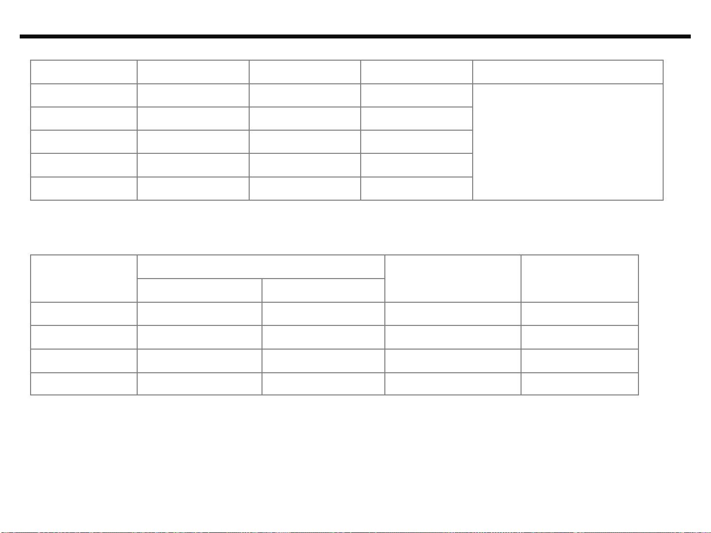
2.1 Band Specification
3
Support Band TX Freq (MHz) RX Freq (MHz)
WCDMA(FDD1) 1920 – 1980 2110 – 2170
WCDMA(FDD2) 1850 – 1910 1930 – 1990
WCDMA(FDD5) 824 – 849 869 – 894
WCDMA(FDD8) 880 – 915 925 – 960
EGSM 880 – 915 925 – 960
GSM850 824 – 849 869 – 894
DCS1800 1710 – 1785 1805 – 1880
PCS1900 1850 – 1910 1930 – 1990
LTE1 1920 – 1980 2110 – 2170
LTE3 1710 – 1785 1805 – 1880
LTE7 2500 – 2570 2620 – 2690
LTE8 880 – 915 925 – 960
LTE20 832 – 862 791 – 821
LTE38 2570 – 2620 2570 – 2620
2. PERFORMANCE
Copyright ⓒ 2019 LG Electronics. Inc. All rights reserved.
Only training and service purposes
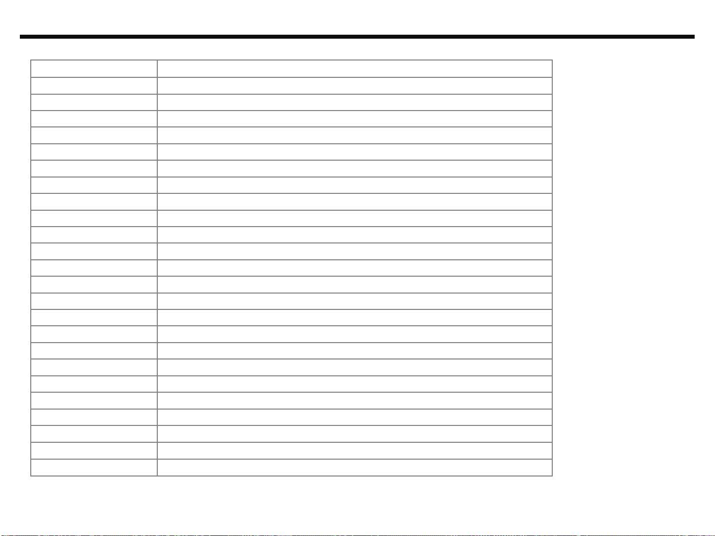
2.2 HW Features
4
List Type / Spec.
1. Phone Type DOP Type
2. Size 156.3mm x 73.9mm x 8.6mm
3. Weight 169g ( with Battery )
4. Battery 3500mAh(Typ), 3400mAh(Min), 3.87V, (Li-ion)
5.Chipset MT6762 2.0GHz Octa core (Quad x Max 2.0G + Quad x Max 1.5G)
2. PERFORMANCE
6. Memory
7. LCD
8. Touch Type 6.088 inch GFF
9. Main Camera (13M)
32GB(eMMC) + 2GB(LPDDR3)
External Memory(SD Card) : Up to 2TB
Size 6.088" HD+ (1560 x 720)
Display Type Active matrix TFT, Transmissive Type
Color 16.7M colors
Resolution HD+(1560(V) x 720(H)), 282ppi
Type CMOS image sensor
Resolution 4160(H) X 3120(V) pixels.
4:3(13.0MP – 4160x3120), 4:3(6.5MP – 2944x2208)
Image Scaling Down
Format Image : JPG, Video : MP4
16:9(9.7MP – 4160x2340), 16:9(4.9MP – 2944x1656)
FullVision(8.0MP – 4160x1920), FullVision(4.0MP – 2944x1360)
1:1(9.7MP – 3120x3120), 1:1(3.4MP – 1840x1840)
Copyright ⓒ 2019 LG Electronics. Inc. All rights reserved.
Only training and service purposes
2.2 HW Features
5
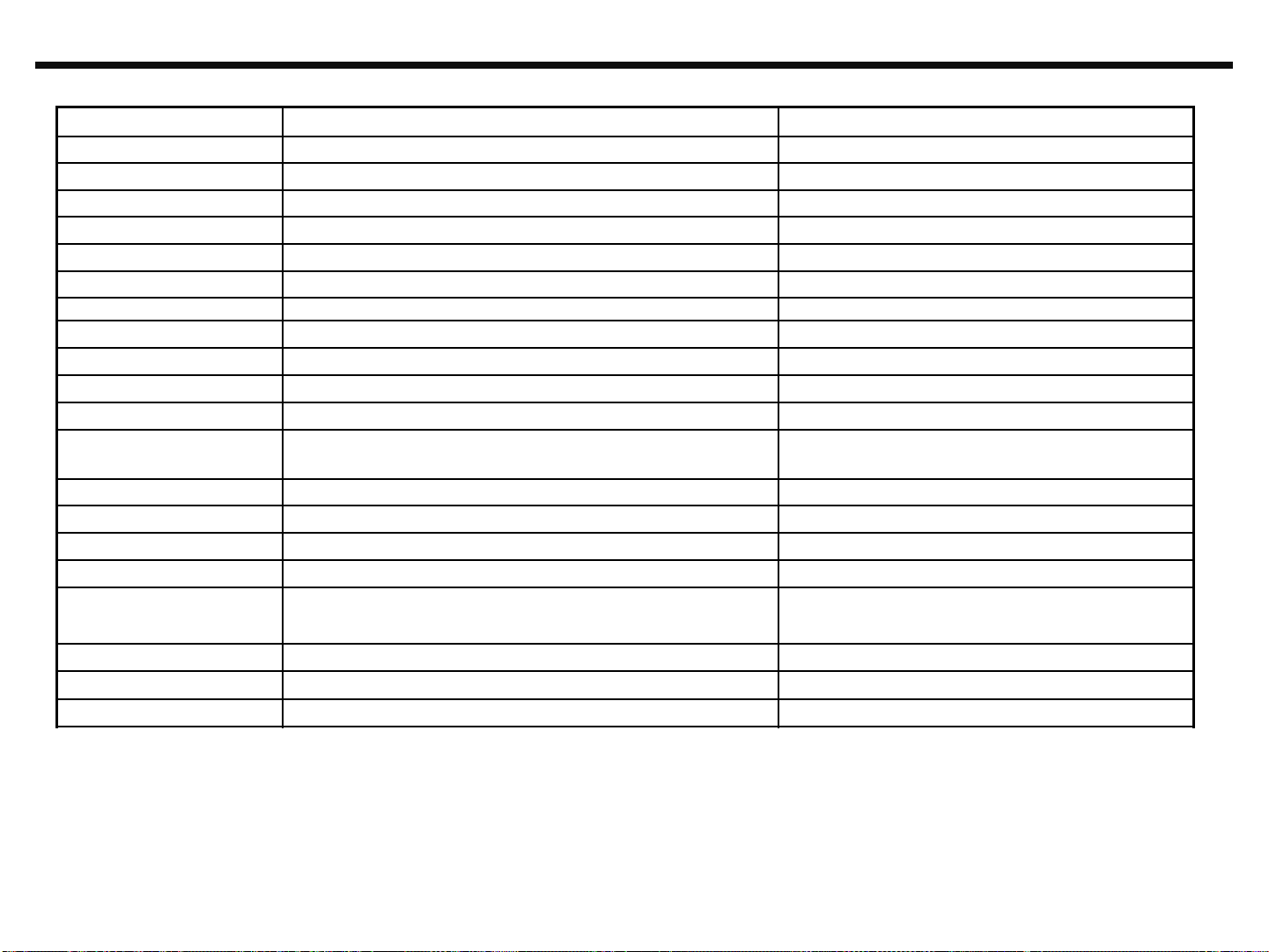
9. Main Wide Camera(W5M) Type CMOS image sensor
Resolution 2560(H) X 1920(V) pixels
Image Scaling Down 4:3(5.0MP – 2560x1920), 4:3(2.5MP – 1824x1368)
16:9(3.7MP – 2560x1440), 16:9(1.9MP – 1824x1026)
FullVision(3.0MP – 2560x1182), Fullvision(1.5MP – 1824x842)
1:1(3.7MP – 1920x1920), 1:1(0.5MP – 720x720)
Format Image : JPG, Video : MP4
2. PERFORMANCE
10. Audio
11. Bluetooth Standard Bluetooth 5.0
12. WLAN Standard IEEE 802.11 b/g/n
Depend on environment 0 ~ 50m (depend on environment)
13. GPS type A-GPS, GLONASS
14. NFC Chipset PN553,NXP
Receiver 08 X 09 X 2.7T Receiver
Speaker 15 X 11 X 2.8T Speaker
Format MP3, AAC, MIDI, EAAC+, OGG, AMR
Effective Distance 10M
Distance 0 m ~ 10 m (depend on environment)
Copyright ⓒ 2019 LG Electronics. Inc. All rights reserved.
Only training and service purposes
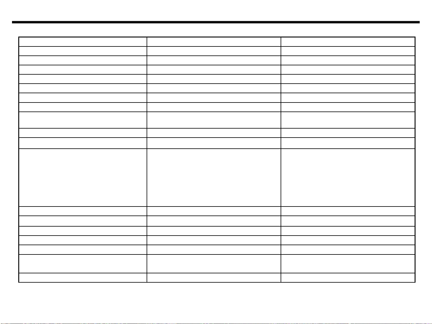
2.3 RSSI Display
6
RSSI BAR GSM RSSI WCDMA RSSI LTE RSSI Comment
2. PERFORMANCE
BAR 5->4
BAR 4->3
BAR 3->2
BAR 2->1
BAR 1->0
- 90dBm± 4dB - 85dBm± 4dB -85dBm ± 4dB
- 95dBm± 4dB - 90dBm± 4dB -95dBm ± 4dB
- 98dBm± 4dB - 96dBm± 4dB -105dBm ± 4dB
- 102dBm± 4dB - 100dBm± 4dB -115dBm ± 4dB
- 104dBm± 4dB - 106dBm± 4dB -128dBm ± 4dB
1. Call Connected & CPIPH Level=-3.3
2. L TE:RSRP
2.4 Current consumption
Stand by
Bluetooth Off Bluetooth Connected
WCDMA Only 11 mA under(DRX=7) 13 mA under(DRX=7) 350mA under(Tx=10dBm) LCD off
GSM Only 11 mA under(PP=5) 13 mA under (PP=5) 360mA under(Lvl=5) LCD off
LTE 11 mA under(LTE 2.56S) 13 mA under(LTE 2.56s) 350mA(@TX 10 dBm)LCD off
Voice Call
(LTE Data connection)
Measurement Condition
VoLTE 11 mA under(LTE 2.56S) 13 mA under(LTE 2.56s) 400mA(@TX 10 dBm) LCD off
Copyright ⓒ 2019 LG Electronics. Inc. All rights reserved.
Only training and service purposes
2.5 Battery bar
7
Battery Bar icon Specification(%)
2. PERFORMANCE
Level 20
Level 19
Level 18
Level 17
Level 16
Level 15
Level 14
Level 13
Level 12
Level 11
Level 10
Level 9
Level 8
Level 7
Level 6
Level 5
Level 4
Level 3
Level 2
Level 1 3 ~ 7
Level 0 0 ~ 2
Low Battery Pop-up
Critical Low battery pop-up
Power off Under 1%
16% 15% : One Time popup (No call) There is no pop-up until 5% if you delete pop-up.
6% 5% : One Time popup (No call) There is no pop-up until 3% if you delete pop-up.
98 ~ 100
93 ~ 97
88 ~ 92
83 ~ 87
78 ~ 82
73 ~ 77
68 ~ 72
63 ~ 67
58 ~ 62
53 ~ 57
48 ~ 52
43 ~ 47
38 ~ 42
33 ~ 37
28 ~ 32
23 ~ 27
16 ~ 22
13 ~ 15
8 ~ 12
Copyright ⓒ 2019 LG Electronics. Inc. All rights reserved.
Only training and service purposes
2. PERFORMANCE
8
2.6 SW Specification
Item Feature Comment
RSSI 0 ~ 5 Levels
Battery Charging 0 ~ 100 Levels
Key Volume 0 ~ 15 Level
Audio Volume 0 ~ 15 Level
Time / Date Display Yes
Multi-Language Yes depending on build language
Quick Access Mode Phone / Messaging / Camera / Gallery / Chrome Phone / Messaging / Camera / Gallery / Chrome
PC Sync No PC Bridge
Speed Dial Yes Voice mail center -> 1 key
Profile Yes not same with feature phone setting
CLIP / CLIR Yes
Phone Book
Last Dial Number Yes
Last Received Number Yes
Last Missed Number Yes
Search by Number/Name Yes
Name / Number / Email / Groups / Postal addresses /
Organizations / IM / Note / Nickname / Website / Event /
There is no limitation on the number of items.
It depends on available memory amount.
Group Yes
Fixed Dial Number Yes
Service Dial Number Yes It depends on operator requirements.
Own Number Yes My Profile (add/edit/delete are supported)
There is no limitation on the number of items.
It depends on available memory amount.
Copyright ⓒ 2019 LG Electronics. Inc. All rights reserved.
Only training and service purposes
2. PERFORMANCE
9
2.6 SW Specification
Voice Memo Yes Support voice recorder
Call Reminder No
Network Selection Automatic
Mute Yes
Call Divert Yes
Call Barring Yes
Call Charge (AoC) No
Call Duration Yes
SMS (EMS)
SMS Over GPRS No
EMS Melody / Picture Send / Receive / Save No
MMS MPEG4
Send / Receive / Save
There is no limitation on the number of items.
It depends on available memory amount.
Yes
EMS does not support.
Send / Receive : Yes
Save : depends on content type
Support video content type list
1. video/mp4
2. video/h263
3. video/3gpp2
4. video/3gpp
Long Message MAX 2000 characters The standard of Open vender
Cell Broadcast Yes CB app supports Cell Broadcast message
Download Over the Web
Game No
Calendar Yes
Memo Yes
World Clock Yes
There is no limitation on the number of items.
It depends on available memory amount.
Copyright ⓒ 2019 LG Electronics. Inc. All rights reserved.
Only training and service purposes
2.6 SW Specification
10
Unit Convert No
Stop Watch Yes
Wall Paper Yes
WAP Browser No Support only web browser via Chrome. WAP stack and wml are not supported.
Download Melody/Wallpaper Yes Over web browser
SIM Lock Yes
SIM Toolkit Yes
MMS Yes Android Message
EONS Yes
CPHS Yes V4.2
ENS No
Camera Yes Front 13M, Rear 13M + W5M
JAVA No
Voice Dial No
IrDa No
Bluetooth Yes Ver. 5.0
FM radio No
GPRS Yes Class 12
EDGE Yes Class 12
Hold / Retrieve Yes
Conference Call Yes Max. 6
DTMF Yes
Memo pad No
TTY No
AMR Yes
SyncML No
IM No Hangout was IM, but it's not preloaded anymore.
Email Yes
2. PERFORMANCE
Copyright ⓒ 2019 LG Electronics. Inc. All rights reserved.
Only training and service purposes

3.TROUBLE SHOOTING
11
3.1 Checking XO Block
The output frequency(26MHz) of VCTXO(X15000) is used as the reference one of MT6176
Checking Flow
START
Image
Check TP1
Is it 26MHz?
NO
Replace U4000 and then check TP1
Is it 26MHz?
NO
The Problem may be
Logic part Refer to
Logic trouble shoot
YES
YES
XO Circuit is OK.
Check next step
XO Circuit is OK.
Check next step
TP1
R4031
U4000
Circuit Diagram
TP1
R4031
Copyright ⓒ 2019 LG Electronics. Inc. All rights reserved.
Only training and service purposes
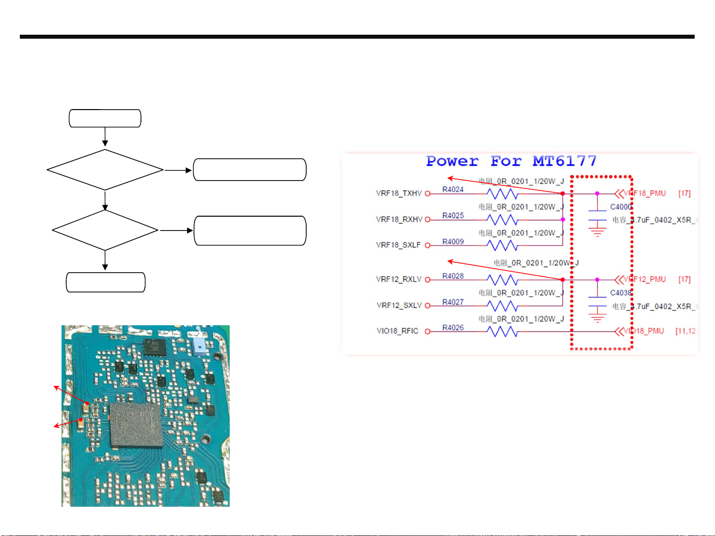
3.2 Transceiver DC Power Supply Circuit
12
Checking Transceiver DC Power Supply Circuit
Checking Flow
START
3.TROUBLE SHOOTING
Circuit Diagram
TP1(1.2V)
C4038
TP2(1.8V)
C4000
Check TP1
+1.2V_RF is OK?
YES
Check TP2
+1.8V_RF is OK?
YES
Check next step
U4000
Image
The Problem may be Logic part
NO
NO
Refer to Logic trouble shoot
The Problem may be Logic part.
Refer to Logic trouble shoot
TP2(1.8V)
TP1(1.2V)
Copyright ⓒ 2019 LG Electronics. Inc. All rights reserved.
Only training and service purposes
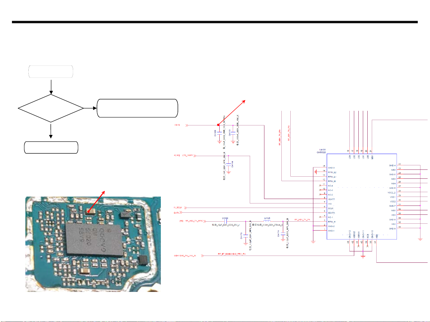
3.3 DC-DC Block
13
Checking DC-DC Block
Checking Flow
START
Check TP1(VSYS)
0.5V ≤ TP1 ≤ 4.2V ?
YES
Check next step
NO
Physical Damage or soldering condition
Check U4103
3.TROUBLE SHOOTING
Circuit Diagram
TP1(VSYS)
C4120
Image
TP1(VSYS)
C4120
U4103
Copyright ⓒ 2019 LG Electronics. Inc. All rights reserved.
Only training and service purposes
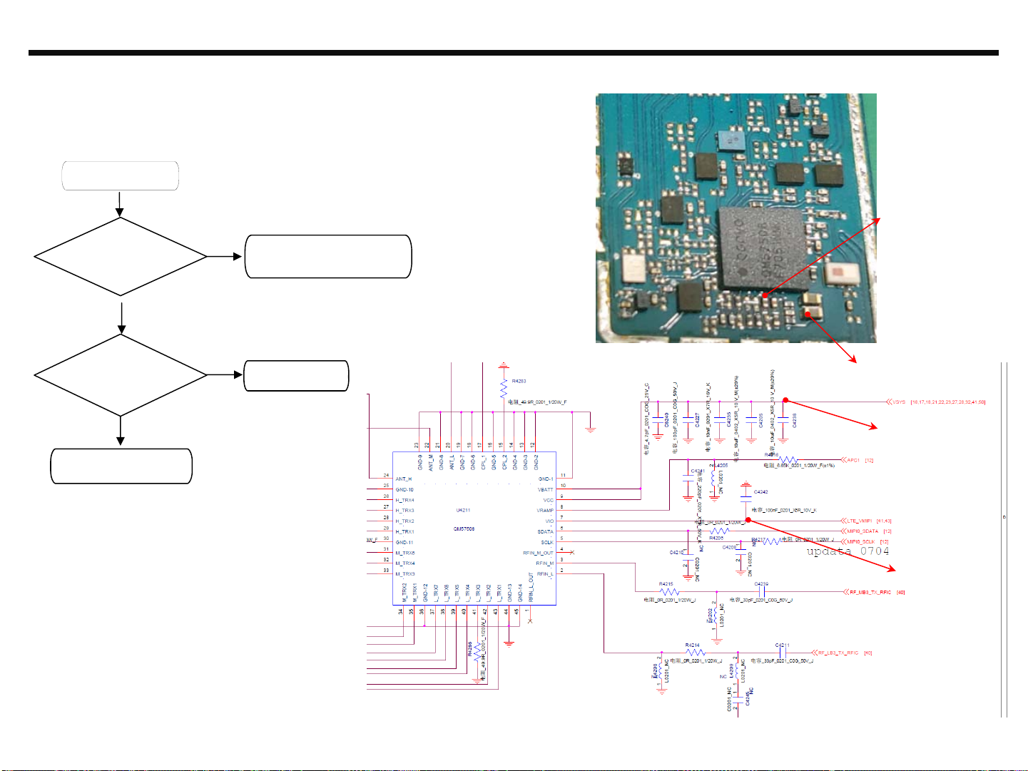
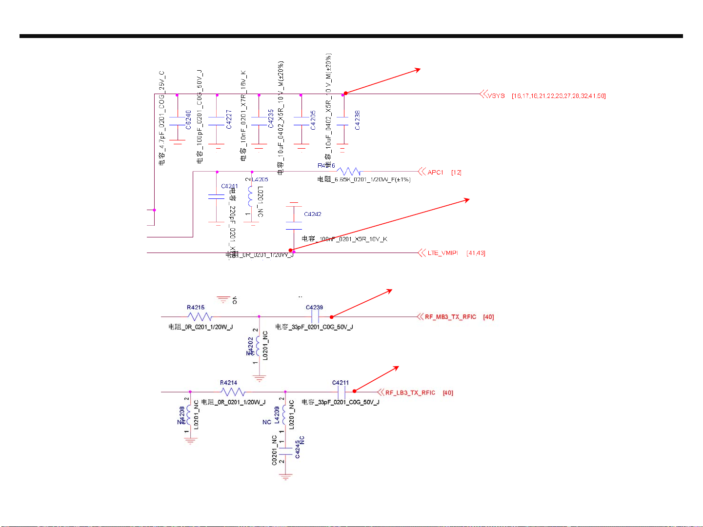
3.4 ASM Block
14
Checking ASM Block
START
3.TROUBLE SHOOTING
Image
Checking Flow
TP2(1.8V)
C4242
Check
TP1, TP2 High Level?
(3.0V≤TP1 ≤4.6V)
(1.65V≤TP2 ≤2.0V)
YES
Check U4211
physical Damage or soldering
condition
OK?
Check Next step
NO
The Problem may be Logic part
Refer to Logic trouble shoot
NOT
GOOD
Replace U4211
U4211
Circuit Diagram
TP1(3.5V)
C4238
TP1(3.5V)
C4238
TP2(1.8V)
C4242
Copyright ⓒ 2019 LG Electronics. Inc. All rights reserved.
Only training and service purposes
3.5 GSM, WCDMA, LTE PART
15
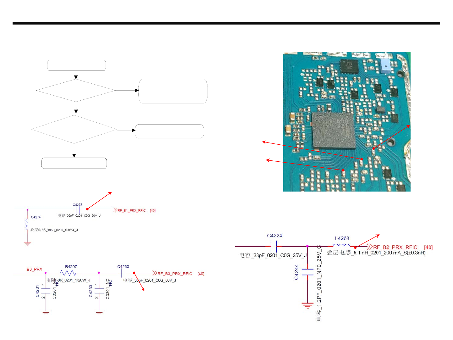
3.5.1 GSM, WCDMA, LTE PART(MB) - PRx
Checking Rx signal path (GSM 1800/1900 WCDMA B1/B2, LTE B1/B3)
Checking Flow
START
3. TROUBLE SHOOTING
Image
TP1/2/3 Signal exist?
Transceiver physical damage
or soldering condition
Check next step
Circuit Diagram
B1
B3/G1800
Check
Check
YES
OK?
NOT GOOD
TP1(B1 PRx)
C4275
NO
Check Component
above RF signal path and
ASM or Switch Block
Replace U4000
TP2(B2/G1900 PRx)
C4230
TP3(B3/G1800 PRx)
L4268
B2/G1900
U4000
(MT6177)
TP1(B1 PRx)
C4275
TP2(B2/G1900 PRx)
L4268
TP3(B3/G1800 PRx)
C4230
Copyright ⓒ 2019 LG Electronics. Inc. All rights reserved.
Only training and service purposes
3.5 GSM, WCDMA, LTE PART
16
3. TROUBLE SHOOTING
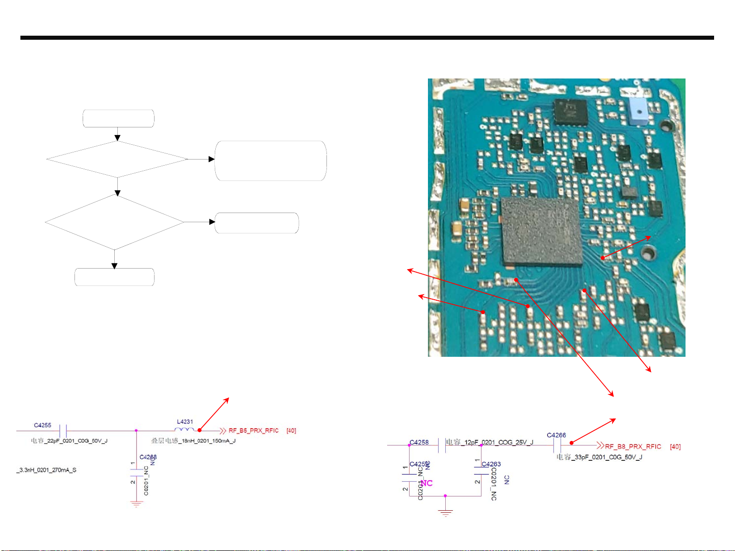
3.5.1 GSM, WCDMA, LTE PART(LB/HB) - PRx
Checking Rx signal path (GSM850/900, WCDMA B5/B8, LTE B7/B8/B20/B38)
Checking Flow
START
Check
TP1/2/3/4/5 Signal exist?
YES
Check
Transceiver physical damage
or soldering condition
OK?
Check next step
NO
NOT GOOD
Check Component
above RF signal path and
ASM or Switch Block
Replace U4000
TP1(B5/G850 PRx)
L4231
TP4(B20 PRx)
C4243
Image
U4000
(MT6177)
TP3(B7 PRx)
C4285
B5/G850
TP1 (B5/G850 PRx)
L4231
Circuit Diagram
TP5(B38 PRx)
C4176
B8/G900
TP2(B8/G900 PRx)
C4266
Copyright ⓒ 2019 LG Electronics. Inc. All rights reserved.
Only training and service purposes
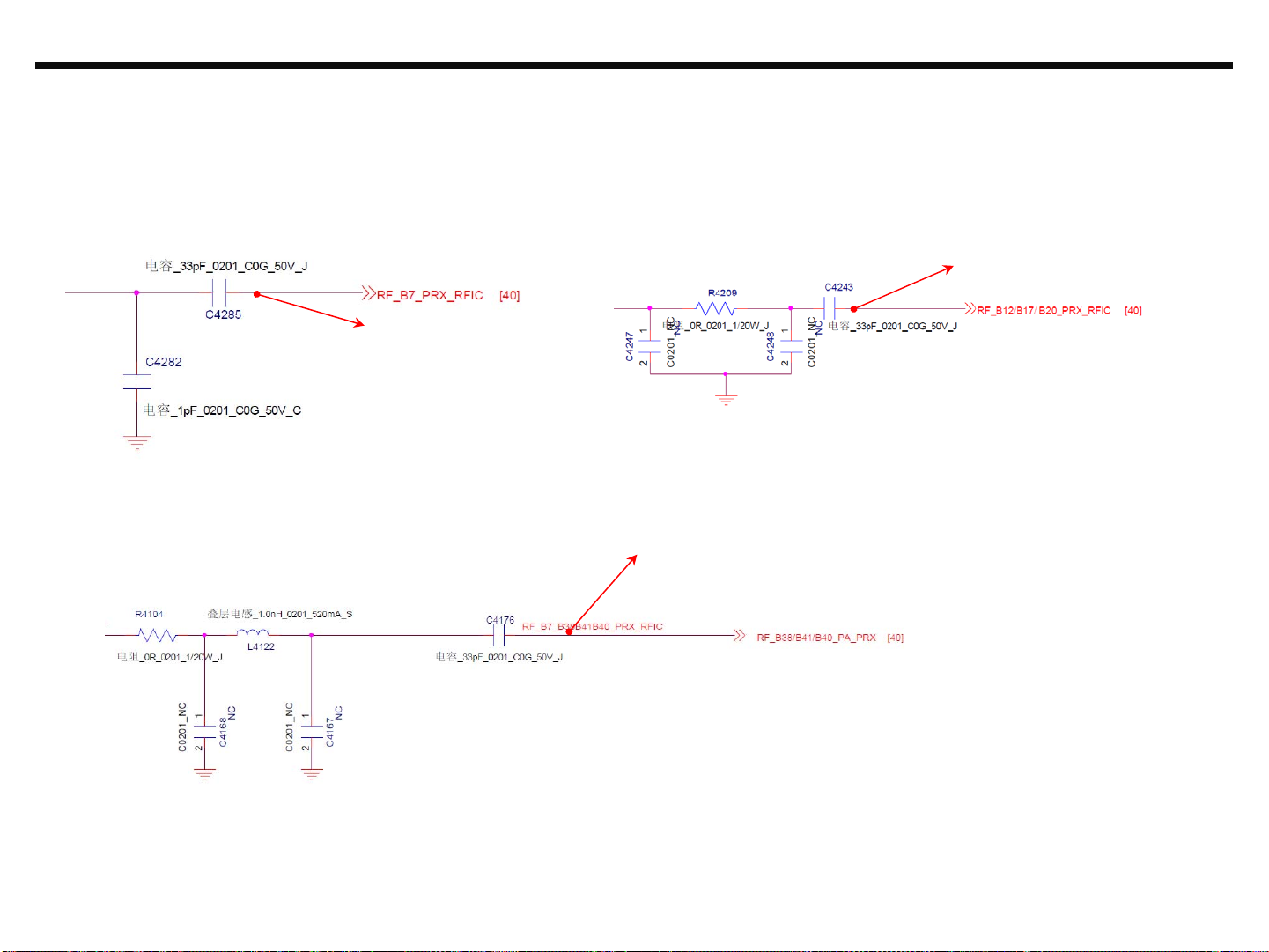
3.5 GSM, WCDMA, LTE PART
17
3.5.1 GSM, WCDMA, LTE PART(LB/HB) - PRx
Checking Rx signal path (GSM850/900, WCDMA B5/B8, LTE B7/B8/B20/B38)
3. TROUBLE SHOOTING
B7
B38
TP3 (B7 PRx)
C4285
B20
TP5(B38 PRx)
C4176
TP4(B20 PRx)
C4243
Copyright ⓒ 2019 LG Electronics. Inc. All rights reserved.
Only training and service purposes
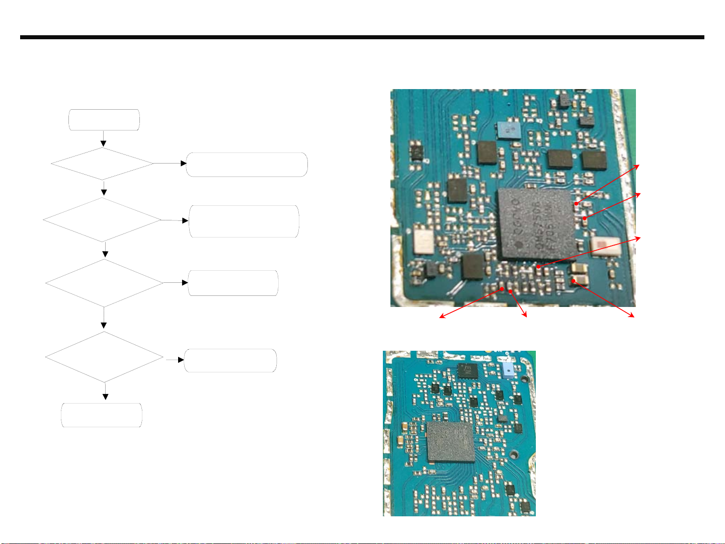
3.5 GSM, WCDMA, LTE PART
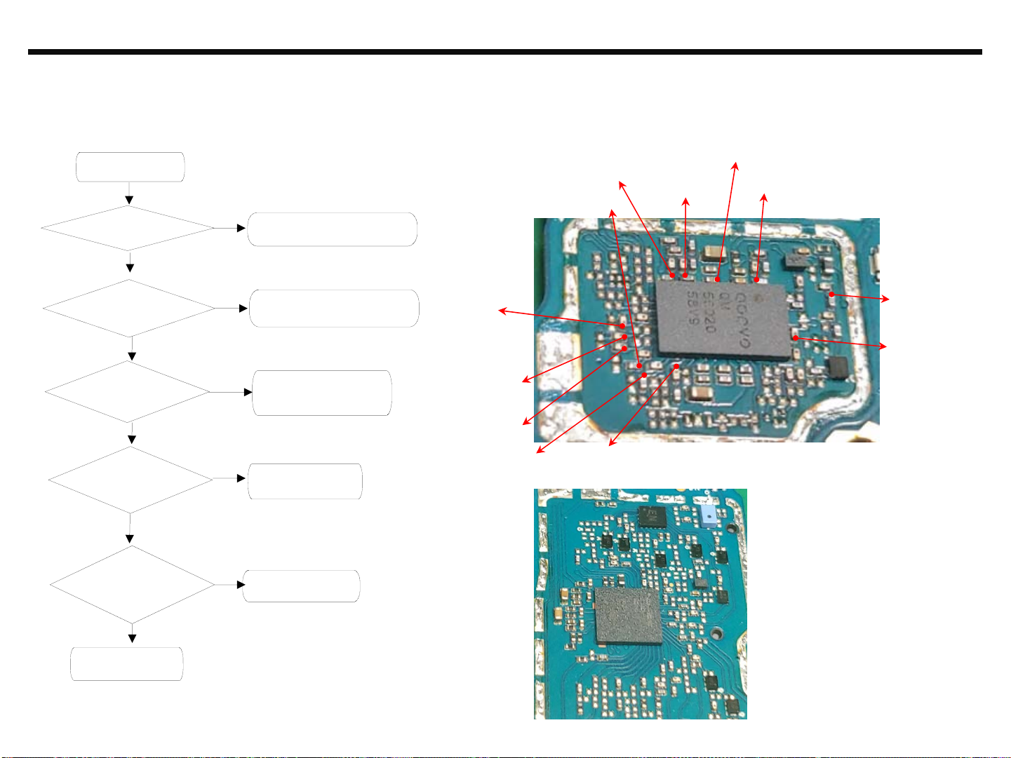
18
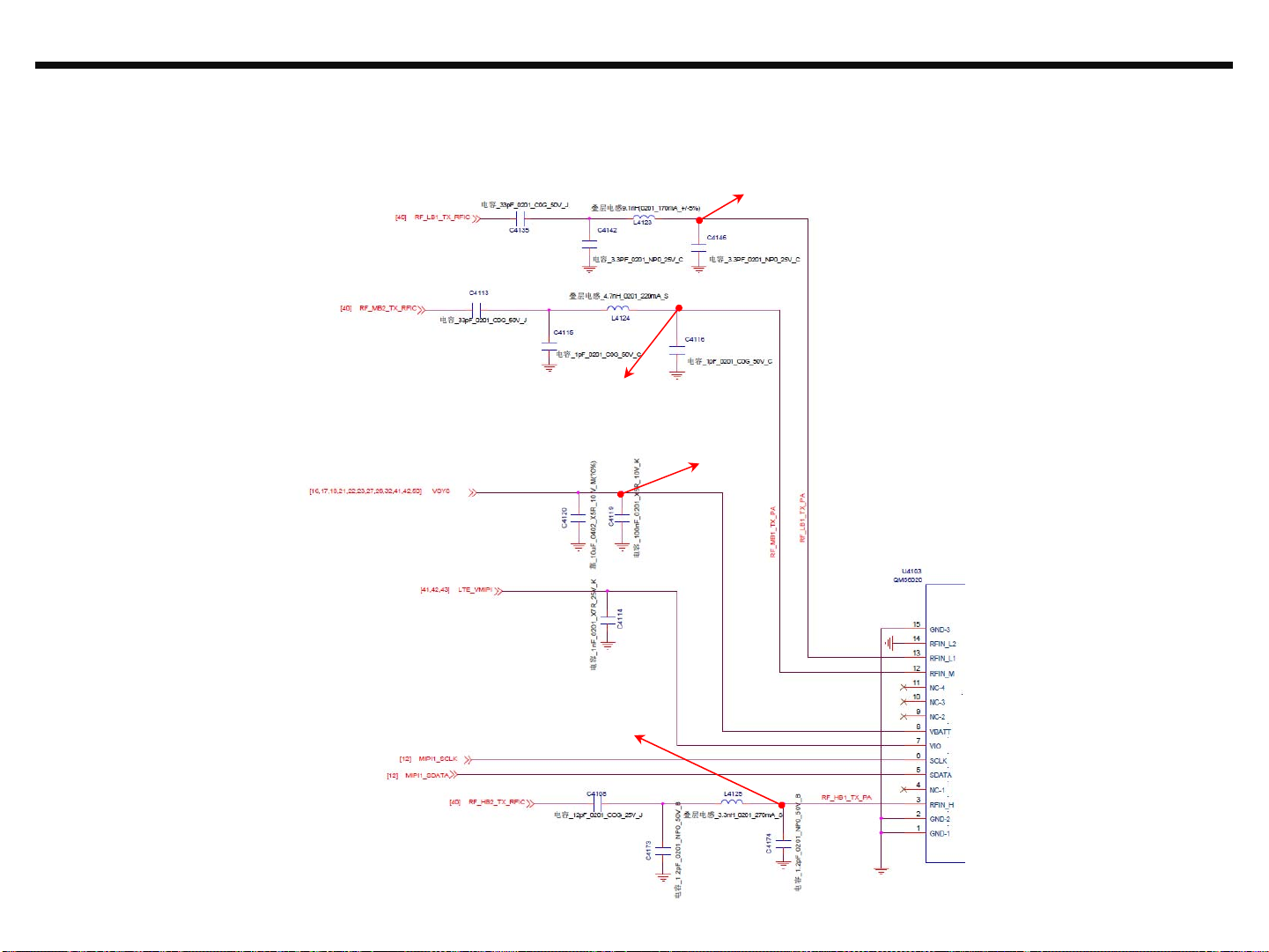
3.5.2 WCDMA, LTE PART - Tx
Checking Tx signal path(WCDMA B1/B2/B5/B8, LTE B1/B3/B7/B8/B20/B38)
3. TROUBLE SHOOTING
Checking Flow
START
Check TP1
VPA_PMU OK?
YES
Check TP1
3.4V≤TP2≤4.4V?
YES
Check TP5~TP14
If LTE of All band
Over 22dBm?
NO
Check TP2~TP4
If WCDMA/LTE of All band
Over 0dBm?
NO
YES
YES
The Problem may be Other part
NO
NO
Check PMIC Logic part
The Problem may be Other part
Check PMIC Logic part
Check component
above RF signal path
and ASM block
Replace U6701
TP11(B8 Tx)
L4121
TP10(B20 Tx)
L4101
TP12(B5 Tx)
L4100
TP6(B3 Tx)
C4126
TP2(LB_input Tx)
C4146
TP7(B2 Tx)
C4128
TP5(B1 Tx)
C4122
Image
TP3
(MB_input TX)
C4116
U4103
(MMPA)
TP1(VBAT)
C4119
TP4(HB_input TX)
C4174
TP8(B38 Tx)
C4105
TP9(B7 Tx)
C4101
Transceiver physical damage
Check
or soldering condition
OK?
Check next step
NOT GOOD
Replace U6701
U4000
(MT6177)
Copyright ⓒ 2019 LG Electronics. Inc. All rights reserved.
Only training and service purposes
3.5 GSM, WCDMA, LTE PART
19
3.5.2 WCDMA, LTE PART - Tx
3. TROUBLE SHOOTING
Circuit Diagram
MMPA Input
LB_input Tx
MB_input Tx
TP2(LB_input Tx)
C4146
TP3(MB_input Tx)
C4116
TP1(VBAT)
C4119
HB_input Tx
TP4(HB_input TX)
C4174
Copyright ⓒ 2019 LG Electronics. Inc. All rights reserved.
Only training and service purposes
3.5 WCDMA, LTE PART
20
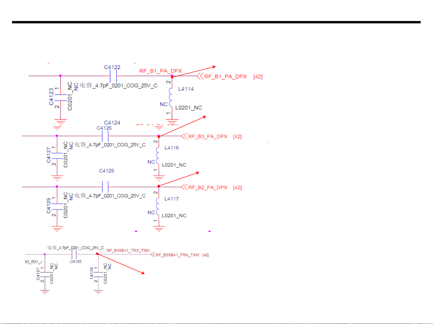
3.5.2 WCDMA, LTE PART - Tx
3. TROUBLE SHOOTING
MMPA Output
Circuit Diagram
TP6(B3 Tx)
C4126
TP7(B2 Tx)
C4128
TP5(B1 Tx)
C4122
B2 Tx
B1 Tx
B3 Tx
B38 Tx
TP8(B38 Tx)
C4105
Copyright ⓒ 2019 LG Electronics. Inc. All rights reserved.
Only training and service purposes
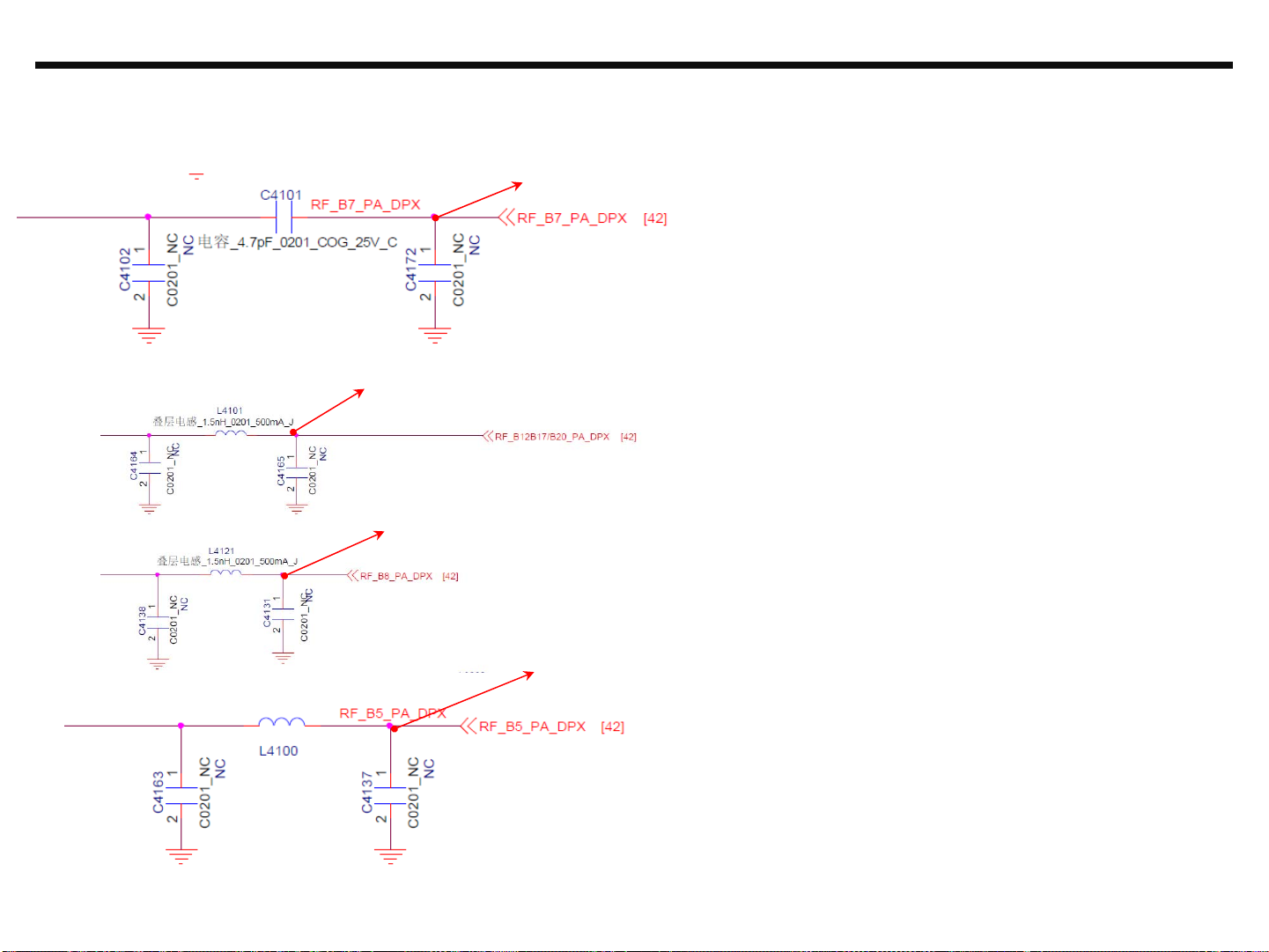
3.5 GSM, WCDMA, LTE PART
21
3.5.2 WCDMA, LTE PART - Tx
3. TROUBLE SHOOTING
MMPA Output
Circuit Diagram
TP10(B20 Tx)
L4101
TP11(B8 Tx)
L4121
TP9(B7 Tx)
B20 Tx
B8 Tx
C4101
B7 Tx
TP12(B5 Tx)
L4100
B5 Tx
Copyright ⓒ 2019 LG Electronics. Inc. All rights reserved.
Only training and service purposes
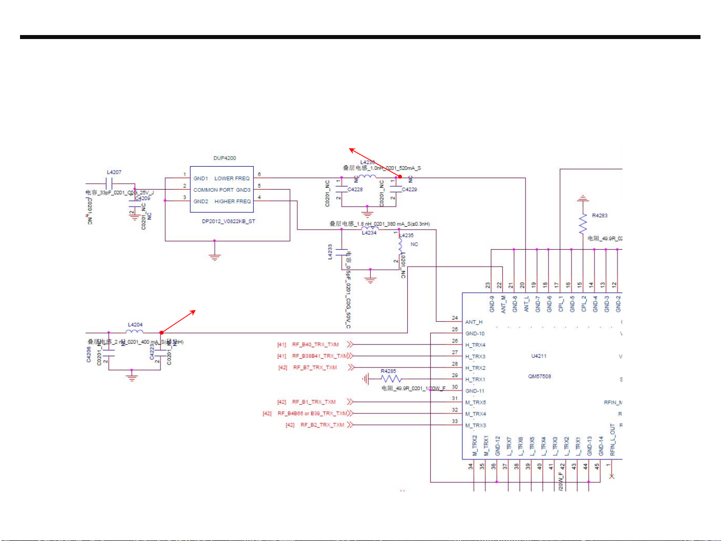
3.5 GSM, WCDMA, LTE PART
22
3.5.3 GSM PART - Tx
Checking Tx signal path(GSM850/900/1800/1900)
Checking Flow
START
3. TROUBLE SHOOTING
Image
Check TP1/2
VBAT/VIO OK?
YES
Check TP5~TP6
If GSM of All band
Over 33/29.5dBm?
NO
Check TP3~TP4
If GSM of All band
Over 0dBm?
NO
Check
Transceiver physical damage
or soldering condition
OK?
Check next step
NO
YES
YES
NOT GOOD
The Problem may be Other part
Check PMIC Logic part
Check component
above RF signal path
and ASM block
Replace U4211
Replace U4211
TP4(LB_input Tx)
C4211
U4000
(MT6177)
U4211
ASM+GSM PA
TP3
(MB_input Tx)
C4239
TP6(GSM MBTx)
C4223
TP5(GSM LB Tx)
L4236
TP2(1.8V)
C4242
TP1(1.2V)
C4238
Copyright ⓒ 2019 LG Electronics. Inc. All rights reserved.
Only training and service purposes
3.5 GSM, WCDMA, LTE PART
23
3. TROUBLE SHOOTING
3.5.3 GSM PART - Tx
Circuit Diagram
TP1(1.2V)
C4238
TP3(MB_input Tx)
C4239
TP2(1.8V)
C4242
MB_input Tx
TP4(LB_input Tx)
C4211
Copyright ⓒ 2019 LG Electronics. Inc. All rights reserved.
GSM Input
LB_input Tx
Only training and service purposes
3.5 WCDMA, LTE PART
24
3.5.3 GSM PART - Tx
GSM Output
3. TROUBLE SHOOTING
Circuit Diagram
GSM850/900 Tx
TP5(GSM LB Tx)
L4236
GSM1800/1900 Tx
TP6(GSM MBTx)
C4223
Copyright ⓒ 2019 LG Electronics. Inc. All rights reserved.
Only training and service purposes

3.5 GSM, WCDMA, LTE PART
25
3.5.4.1 GSM,WCDMA, LTE PART - DRX
Checking DRX RF signal path
(GSM850/900/1800/1900 WCDMA B1/B2/B5/B8 LTE B1/B3/B8/B20)
Checking Flow
3. TROUBLE SHOOTING
Image
TP1(VDD)
C4311
TP2(VIO)
C4313
START
Check TP1, TP2 High Level?
(2.7V≤TP1 ≤2.8V)
(1.7V≤TP2 ≤1.9V)
YES
Check SW4300/DIP4300
physical Damage or soldering condition
OK?
TP3/4/5/6/7/8 Signal exist?
Transceiver physical damage
Check
YES
Check
or soldering condition
NOT GOOD
NO
NOT
GOOD
The Problem may be Logic part
Refer to Logic trouble shoot
Replace SW4300/DIP4300
NO
Check Component
above RF signal path and
ASM or Switch Block
Replace U4000
TP6(WB1/LTE B1 DRx)
C4342
TP7(G1800/LTE B3 DRx)
L4306
TP1(VDD)
C4311
Circuit Diagram
SW4300
TP8(G1900/
WB2 DRx)
L4309
DIP4300
TP3 (G850/
WB5 DRx)
C4354
TP4(G900/WB8
/LTE B8 DRx)
C4370
TP5 (B20 DRx)
C4320
TP2(VIO)
C4313
OK?
Check Next step
Copyright ⓒ 2019 LG Electronics. Inc. All rights reserved.
Only training and service purposes
3.5 GSM, WCDMA, LTE PART
26
3.5.4.1 GSM,WCDMA, LTE PART - DRX
Checking DRX RF signal path
(GSM850/900/1800/1900 WCDMA B1/B2/B5/B8 LTE B1/B3/B8/B20)
3. TROUBLE SHOOTING
TP3(G850/WB5 DRx)
C4354
TP4(G900/WB8/LTE B8 DRx)
C4370
B20 DRX
B1 DRX
TP6(WB1/LTE B1 DRx)
C4342
TP7(G1800/LTE B3 DRx)
L4306
TP8(G1900/WB2 DRx)
L4309
TP5(B20 DRx)
C4320
Copyright ⓒ 2019 LG Electronics. Inc. All rights reserved.
Only training and service purposes
3.5 GSM, WCDMA, LTE PART
27
3.5.4.2 GSM,WCDMA, LTE PART - DRX
Checking DRX RF signal path (LTE B7/B38)
Checking Flow
START
3. TROUBLE SHOOTING
Image
Check J4500/J4303
Connected properly?
YES
Check TP1, TP2 High Level?
(2.7V≤TP1 ≤2.8V)
(1.7V≤TP2 ≤1.9V)
YES
Check W4301
physical Damage or soldering condition
OK?
Check
TP3/4 Signal exist?
YES
Check
Transceiver physical damage
or soldering condition
NO
NOT
GOOD
NO
NOT GOOD
Re-connet coaxial cable properly
The Problem may be Logic part
Refer to Logic trouble shoot
Replace SW4301
Check Component
above RF signal path and
ASM or Switch Block
Replace U4000
TP2(VIO)
C4308
J4500 J4303
(Coaxial Cable Connector)
TP4(B7 DRx)
R4332
SW4301
TP3(B38 DRx)
R4330
TP1(VDD)
C4310
OK?
Check Next step
Copyright ⓒ 2019 LG Electronics. Inc. All rights reserved.
Only training and service purposes
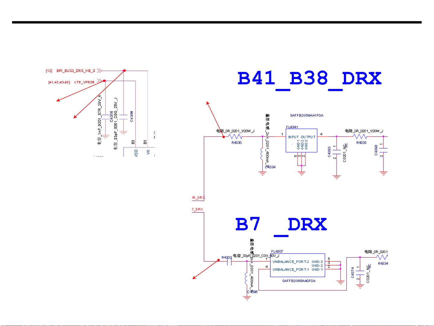
3.5 GSM, WCDMA, LTE PART
28
3.5.4.2 GSM,WCDMA, LTE PART - DRX
Checking DRX RF signal path (LTE B7/B38)
TP1(VDD)
R4310
TP2(VIO)
C4308
3. TROUBLE SHOOTING
Circuit Diagram
TP3(B38 DRx)
R4330
TP4(B7 DRx)
R4332
Copyright ⓒ 2019 LG Electronics. Inc. All rights reserved.
Only training and service purposes
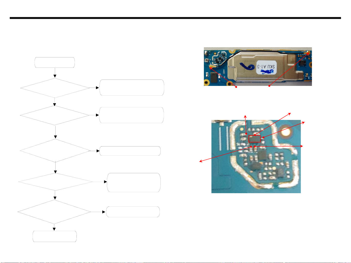
3.6 Power
29
Checking Power signal (Battery connector, Power Key, PMIC Regulator)
Checking Flow
START
BATTERY
CONNECTOR(J2100)
Battery voltage
higher than 3.6V?
YES
Press PWR Key
TP1(TP3204) high to low?
YES
Check
MT6357 Core Voltage level?
NO
Change or charging
the Battery
NO
Check POWER_KEY S/W
NO
L1600, L1601, L1602
(Check MT6357)
3. TROUBLE SHOOTING
TP1 (TP3204)
YES
Check
MT6357 IO Voltage level?
YES
Check Main Clock level ?
YES
Check
Battery connector(J2100)
YES
END
NO
NO
NO
L1604(TP2)
(Check MT6357)
X1800(TP3)
(Check MT6357)
Change MT6357
And Return to Start
TP2(L1604)
TP3
(X1800)
Core DC/DC
Inductor(L1600,L1601, L1602)
Copyright ⓒ 2019 LG Electronics. Inc. All rights reserved.
Only training and service purposes
 Loading...