

LG LM-240WU4-SLA1 Service manual
( ● ) Preliminary Specification
( ● ) Final Specification
LM240WU4
Liquid Crystal Display
Product Specification
SPECIFICATION
FOR
APPROVAL
24.0” WUXGA TFT LCDTitle
BUYER
MODEL
www.jxlcd.com
www.jxlcd.com
APPROVED BY
/
/
/
SIGNATURE
DATE
SUPPLIER LG Display Co., Ltd.
*MODEL LM240WU4
SUFFIX SLA1
*When you obtain standard approval,
please use the above model name without suffix
APPROVED BY
REVIEWED BY
PREPARED BY
SIGNATURE
DATE
Please return 1 copy for your confirmation with
your signature and comments.
Ver. 1.0 Apr. 21 . 2008
MNT Products Engineering Dept.
LG. Philips LCD Co., Ltd
1/ 34
LM240WU4
4
OPTICAL SFECIFICATIONS
72EMC
29
Liquid Crystal Display
Product Specification
Contents
No ITEM Page
COVER
CONTENTS
RECORD OF REVISIONS
1 GENERAL DESCRIPTION
2 ABSOLUTE MAXIMUM RATINGS
3 ELECTRICAL SPECIFICATIONS
3-1 ELECTRICAL CHARACTREISTICS
3-2 INTERFACE CONNECTIONS
3-3 SIGNAL TIMING SPECIFICATIONS
3-4 SIGNAL TIMING WAVEFORMS
3-5 COLOR INPUT DATA REFERNECE
3-6 POWER SEQUENCE
www.jxlcd.com
3-7 POWER SEQUENCE FOR INVERTER
5 MECHANICAL CHARACTERISTICS
www.jxlcd.com
1
2
3
4
5
6
6
8
14
15
16
17
18
19
25
6 RELIABLITY
7 INTERNATIONAL STANDARDS
7-1 SAFETY
-
8PACKING
8-1 DESIGNATION OF LOT MARK
8-2 PACKING FORM
8-3 PALLET FORM 32
9 PRECAUTIONS 33
Ver. 1.0 Apr. 21 . 2008
28
29
29
30
30
31
2/ 34

Product Specification
18
(
)
31
Updated the Packing Form
RECORD OF REVISIONS
LM240WU4
Liquid Crystal Display
Revision
No
0.0 Oct.19. 2007 - First Draft(Preliminary)
0.1 Dec. 20. 2007 4,6,25 TBD is update
1.0 Apr. 21. 2008 4 Update the Power Consumption
Revision Date Page Description
Change the Inverter Power Sequence
T1 Min 1→20, T2 Min 200→500
19
26,27
7 Update the Inverter Input Current, Power
8
13
19 Update the Chromaticity
www.jxlcd.com
www.jxlcd.com
26, 27
Change the Min CR (600→700), Tr/Tf (TBD/TBD→6.0/7.0)
Update the Mechanical Drawing (Tilt 1.0→1.4)
: Inverter Input CNT is moved 4mm inside
Change the Inverter Vbr Min Vlotage (0V→0.3V)
Change the T2 Refer page (page 14 → page 17)
Change the Inverter Vbr Min Vlotage (0V→0.3V)
Updated the Mechanical Drawing
Ver. 1.0 Apr. 21 . 2008
3/ 34
LM240WU4
LM
240WU4isa
Color
Active
Matrix
Liquid
Crystal
Display
withanintegral
Cold
Cathode
Fluorescent
high
high
T
Controller
(H)
)
+24.0V
() () () (yp)
Power Consumption
Total
82
Watt (Typ.) ( 7.02 Watt
@V
LCD
8Watt@V
)
Liquid Crystal Display
Product Specification
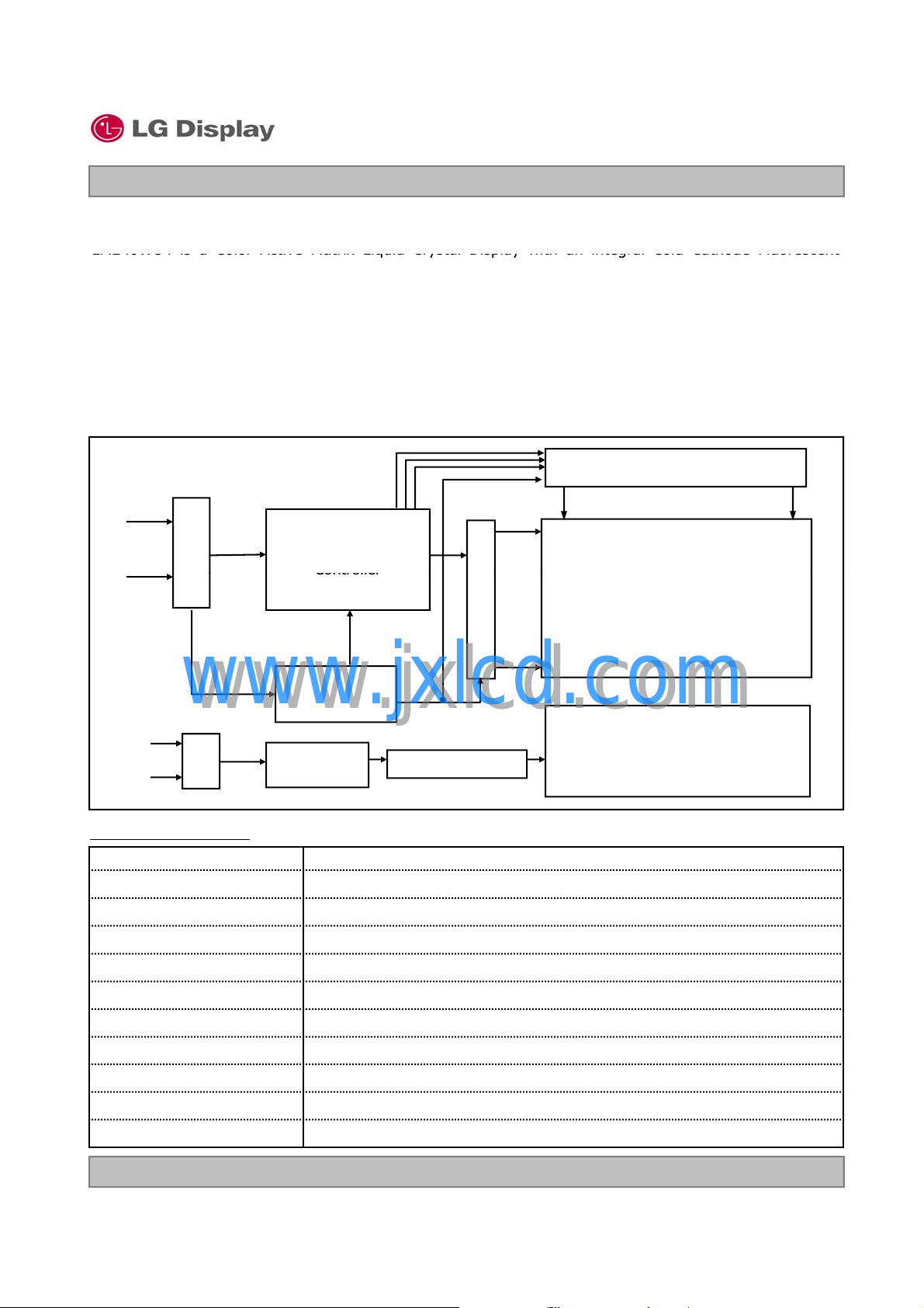
1. General Description
Lamp(CCFL) backlight system. The matrix employs a-Si Thin Film Transistor as the active element.
It is a transmissive type display operating in the normally black mode. It has a 24inch diagonally measured
active display area with WUXGA resolution (1200 vertical by 1920 horizontal pixel array)
Each pixel is divided into Red, Green and Blue sub-pixels or dots which are arranged in vertical stripes.
Gray scale or the brightness of the sub-pixel color is determined with a 8-bit gray scale signal for each dot,
thus, presenting a palette of more than 16,7M(True) colors.
It has been designed to apply the 8Bit 2 port LVDS interface.
It is intended to support displays where high brightness, super wide viewing angle,
color saturation, and
color are important.
RGB
LVDS
2port
+12.0V
GND
CN1
(30pin)
+12.0V
www.jxlcd.com
www.jxlcd.com
CN2
(14Pin)
Timing
Power Circuit
Block
Inverter
Block
2pin x 7CNs (High)
Gate
Driver Circuit
General Features
Active Screen Size 24.1 inches(61.32cm) diagonal
Outline Dimension 546.4
Pixel Pitch 0.270 mm x 0.270 mm
x 352.0(V) x 40.3(D) mm(Typ.
Source Driver Circuit
S1 S1920
G1
FT - LCD Panel
(1920 × RGB × 1200 pixels)
G1200
Back light Assembly
(U-Shape 7CCFL)
Pixel Format 1920 horiz. By 1200 vert. Pixels RGB stripes arrangement
Color Depth 8-bit, 16,777,216 colors
Luminance, White 400 cd/m
Viewing Angle(CR>10) View Angle Free (R/L 178(Typ.), U/D 178(Typ.))
Weight 2790 g (typ.)
Display Operating Mode Transmissive mode, normally black
Surface Treatment Hard coating(3H), Anti-glare treatment of the front polarizer
Ver. 1.0 Apr. 21 . 2008
2
( Center 1 points)
71.
, 64.
DDB
4/ 34
Product Specification
The following
Wet bulb temperature should be 39
Max, and no condensation of water
0
2. Absolute Maximum Ratings
are maximum values which, if exceeded, may cause faulty operation or damage to the unit.
Table 1. ABSOLUTE MAXIMUM RATINGS
LM240WU4
Liquid Crystal Display
Parameter Symbol
Power Input Voltage
Operating Temperature
Storage Temperature
Operating Ambient Humidity
Storage Humidity
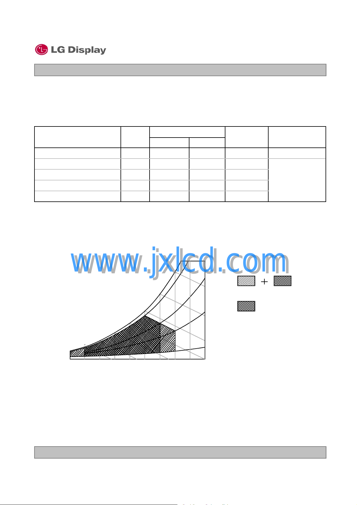
Note : 1. Temperature and relative humidity range are shown in the figure below.
Note : 2. Maximum Storage Humidity is up to 40℃, 70% RH only for 4 corner light leakage Mura.
www.jxlcd.com
www.jxlcd.com
Wet Bulb
Temperature [C]
20
10
VLCD -0.3 14 Vdc at 25 ± 2°C
TOP 050
TST -20 60
HOP 10 90 %RH
HST 10 90 %RH
C
50
40
30
Values
Min Max
°
90%
60
60%
40%
10%
Units Notes
°C
°C
.
Storage
Operation
Humidity [(%)RH]
1, 2
Ver. 1.0 Apr. 21 . 2008
10 20 30 40 50 60 70 800-20
Dry Bulb Temperature [C]
5/ 34
LM240WU4
3-1. El
Parameter
Symbol
Unit
Notes
time, we recommend the bandwidth configuration of oscilloscope is to be under 20Mhz
Liquid Crystal Display
Product Specification
3. Electrical Specifications
ectrical Characteristics
It requires two power inputs. One is employed to power the LCD electronics and to drive the TFT array and
liquid crystal. The second input power for the CCFL, is typically generated by an inverter. The inverter is an
external unit to the LCDs.
Table 2-1. ELECTRICAL CHARACTERISTICS
Values
Min Typ Max
MODULE :
Power Supply Input Voltage V
Permissive Power Input Ripple V
Power Supply Input Current I
Power Consumption
Rush current IRUSH --3.0A4
Note :
1. Permissive power ripple should be measured under V
2. The specified current and power consumption are under the V
whereas mosaic pattern(8 x 6) is displayed and f
3. The current is specified at the maximum current pattern.
4. The duration of rush current is about 2ms and rising time of power Input is 1ms(min.).
www.jxlcd.com
www.jxlcd.com
LCD 11.4 12.0 12.6 Vdc
RF 400 mVp-p 1
LCD
PLCD TYP - 7.02 8.07 Watt 2
PLCD MAX - 9.18 10.56 Watt 2
- 585 673 mA 2
- 765 880 mA 3
=12.0V, 25 ± 2°C,fV=60Hz condition and At that
LCD
=12.0V, 25 ± 2°C,fV=60Hz condition
is the frame frequency.
V
LCD
.
White Pattern
< Permissive Power Input Ripple (V
Ver. 1.0 Apr. 21 . 2008
=12.0V, 25 ± 2°C,f
LCD
Black Pattern
=60Hz) >
V
6/ 34
Typical current pattern
(White : 255Gray, Black : 0Gray)
p
value at the typical lamp current on condition of continuous operating at 25
±
2
C
LM240WU4
Liquid Crystal Display
Product Specification
Maximum current pattern
Mosaic Pattern(8 x 6)
< Power consumption (V
Table 2-2. INVERTER ELECTRICAL CHARACTERISTICS
Parameter Symbol Condition
Inverter :
Input Voltage V
Input Current I
Input Power P
B/L on/off control V
Brightness Adj V
www.jxlcd.com
www.jxlcd.com
LAMP :
Life time
DDB
B
ON/OFF
BR
V
= 3.3V
VBR= 3.3V
Lamp ON = High
Lamp OFF =Low
=12.0V, 25 ± 2°C,f
LCD
White Pattern
=60Hz) >
V
Values
Min. Typ. Max.
22 24.0 26 V 1
- 2.7 3.2 A2
- 64.8 84.5 Watt 2
2.0 - 5.0 V
0.0 - 0.8 V
0.3 -3.3V3
40,000 Hrs 4
Unit Notes
Notes :
1. The input voltage ripple is limited below 400mVp-p.
2. The specified current and power consumption are under the typical supply Input voltage, 24V.
3. Dimming Start voltage will be set at 3.2V±3%(0.096V) considering IC and components deviation.
4. The life is determined as the time at which luminance of the lamp is 50% compared to that of initial
5. Electrical characteristics are determined after the unit has been ‘ON’ and stable for approximately
30min in a dark environment at 25 °C± 2°C.
6. In case of the difference in measured values due to the difference
of measuring device was found, correlated value will be used after discussions between both parties.
Ver. 1.0 Apr. 21 . 2008
°
.
7/ 34
Liquid Crystal Display
ypy
p
11
FR3P
Plus signal of odd channel 3 (LVDS)
26
OPEN
NC
Product Specification
3-2. Interface Connections
3-2-1. LCD Module
-LCD Connector(CN1). : KDF71G-30S-1H (Manufactured by HIROSE) or Equivalent
ISL100-L30B-C23(UJU), GT103-30S-H23 (LS cable)
- Mating Connector : FI-XC30C2L (Manufactured by JAE) or Equivalent
Table 3 MODULE CONNECTOR(CN1) PIN CONFIGURATION
No Symbol Description No Symbol Description
LM240WU4
1FR0M
2FR0P
3FR1M
4FR1P
5FR2M
6FR2P
7 GND
8FCLKINM
9FCLKINP
10 FR3M
12 SR0M
13 SR0P
14 GND
15 SR1M
Minus signal of odd channel 0 (LVDS)
Plus signal of odd channel 0 (LVDS)
Minus signal of odd channel 1 (LVDS)
Plus signal of odd channel 1 (LVDS)
Minus signal of odd channel 2 (LVDS)
Plus signal of odd channel 2 (LVDS)
Ground
Minus signal of odd clock channel (LVDS)
Plus signal of odd clock channel (LVDS)
www.jxlcd.com
www.jxlcd.com
Minus signal of odd channel 3 (LVDS)
Minus signal of even channel 0 (LVDS)
Plus signal of even channel 0 (LVDS)
Ground
Minus signal of even channel 1 (LVDS)
16 SR1P
17 GND
18 SR2M
19 SR2P
20 SCLKINM
21 SCLKINP
22 SR3M
23 SR3P
24 GND
25 OPEN
27 DCR_OUT
ODC on/off
28
29 VLCD
30 VLCD
Plus signal of even channel 1 (LVDS)
Ground
Minus signal of even channel 2 (LVDS)
Plus signal of even channel 2 (LVDS)
Minus signal of even clock channel (LVDS)
Plus signal of even clock channel (LVDS)
Minus signal of even channel 3 (LVDS)
Plus signal of even channel 3 (LVDS)
Ground
NC
Dynamic C/R output
ODC_ON_OFF_Control [* note 4 ]
L : ODC_ON , H : ODC_OFF
Default : ODC_ON ( No connection)
Power Supply +12.0V
Power Supply +12.0V
Note: 1. All GND(ground) pins should be connected together and to Vss which should also be connected to
the LCD’s metal frame.
2. All V
Ver. 1.0 Apr. 21 . 2008
LCD (power input) pins should be connected together.
3. Input Level of LVDS signal is based on the IEA 664 Standard.
4. In ODC off Case , When Power Start up, Sequence must keep as : V
* T2 : Time interval between V
LCD > T2 > ODC_OFF (‘H’)
LCD and RGB data, refer to page 17.
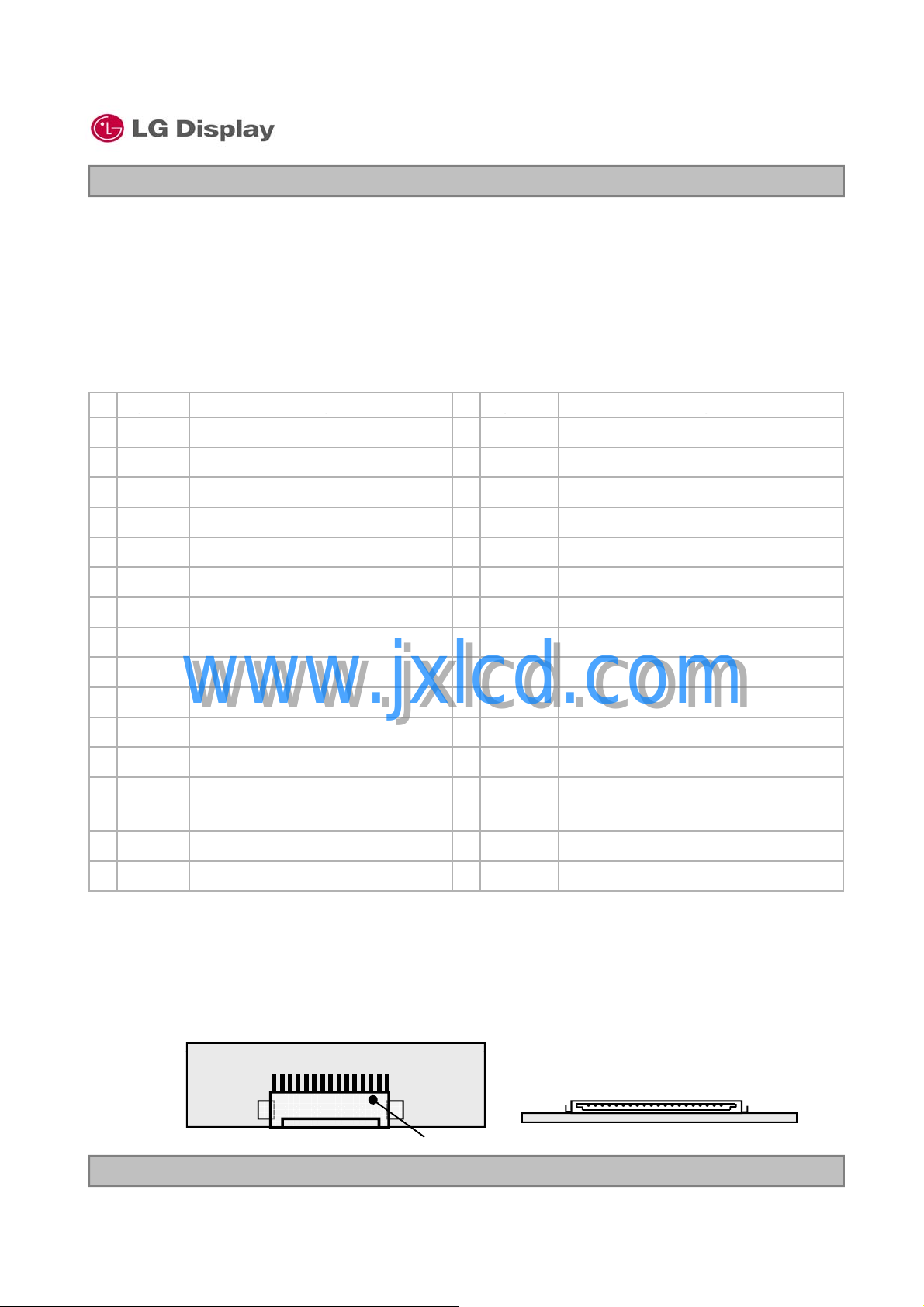
User Connector Diagram
1
30
#1 #30
Rear view of LCM
KDF71G-30S-1H(HIROSE)
8/ 34
LM240WU4
16
TTL Input (B6)
D1644Power Supply for LVDS
LVDS V
CC
T
T
Liquid Crystal Display
Product Specification
Table 4. REQUIRED SIGNAL ASSIGNMENT FOR Flat Link (TI:SN75LVDS83) Transmitter
Pin # Require SignalPin Name Pin # Require SignalPin Name
1 Power Supply for TTL InputVCC 29 Ground pin for TTLGND
2 TTL Input (R7)D5 30 TTL Input (DE)D26
3 TTL Input (R5)D6 31 TTL Level clock InputTXCLKIN
4 TTL Input (G0)D7 32 Power Down InputPWR DWN
5 Ground pin for TTLGND 33 Ground pin for PLLPLL GND
6 TTL Input (G1)D8 34 Power Supply for PLLPLL VCC
7 TTL Input (G2)D9 35 Ground pin for PLLPLL GND
8 TTL Input (G6)D10 36 Ground pin for LVDSLVDS GND
9 Power Supply for TTL InputVCC 37 Positive LVDS differential data output 3
10 TTL Input (G7)D11 38 Negative LVDS differential data output 3
11 TTL Input (G3)D12 39 Positive LVDS differential clock output
12 TTL Input (G4)D13 40 Negative LVDS differential clock output
13 Ground pin for TTLGND 41 Positive LVDS differential data output 2
14 TTL Input (G5)D14 42 Negative LVDS differential data output 2
www.jxlcd.com
15 TTL Input (B0)D15 43 Ground pin for LVDSLVDS GND
17 Power Supply for TTL InputVCC 45 Positive LVDS differential data output 1
18 TTL Input (B7)D17
19 TTL Input (B1)D18
20 TTL Input (B2)D19
22
23 TTL Input (B4)D21
24 TTL Input (B5)D22
25 TTL Input (RSVD)D23
www.jxlcd.com
46 Negative LVDS differential data output 1
47 Positive LVDS differential data output 0
48 Negative LVDS differential data output 0
49 Ground pin for LVDSLVDS GND21 Ground pin for TTL InputGND
TL Input (B3)D20
50
51 TTL Input (R0)D0
52 TTL Input (R1)D1
53 Ground pin for TTLGND
TxOUT3+
TxOUT3-
TXCLKOUT+
TXCLKOUT-
TXOUT2+
TXOUT2-
TXOUT1+
TXOUT1-
TXOUT0+
TXOUT0-
TL Input (R6)D27
26 Power Supply for TTL InputVCC 54 TTL Input (R2)D2
Notes : Refer to LVDS Transmitter Data Sheet for detail descriptions.
Ver. 1.0 Apr. 21 . 2008
55 TTL Input (R3)D327 TTL Input (HSYNC)D24
56 TTL Input (R4)D428 TTL Input (VSYNC)D25
9/ 34
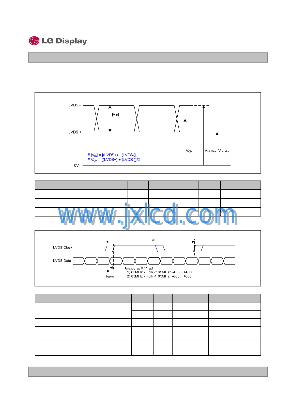
LVDS Input characteristics
F
V
-±3%-
1. DC Specification
LM240WU4
Liquid Crystal Display
Product Specification
Description Symbol Min Max Unit Notes
LVDS Differential Voltage |VID| 100 600 mV -
LVDS Common mode Voltage V
LVDS Input Voltage Range V
www.jxlcd.com
2. AC Specification
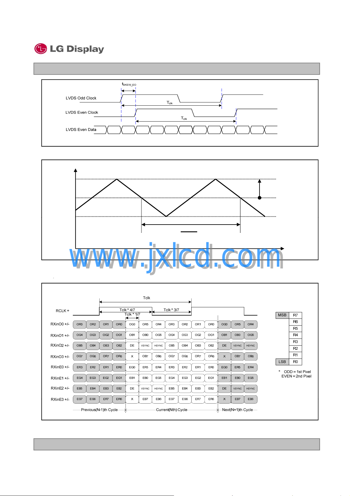
LVDS Clock to Data Skew Margin
LVDS Clock to Clock Skew Margin (Even to Odd) t
Maximum deviation
of input clock frequency during SSC
Maximum modulation frequency
of input clock during SSC
www.jxlcd.com
Description Symbol Min Max Unit Notes
CM
IN
t
SKEW
t
SKEW
SKEW_EO
DE
F
MOD
0.6 1.8 V -
0.3 2.1 V -
- 400 + 400 ps 85MHz > Fclk ≥ 65MHz
- 600 + 600 ps 65MHz > Fclk ≥ 25MHz
-1/7 + 1/7 T
- 200 KHz -
clk
-
Ver. 1.0 Apr. 21 . 2008
10 / 34
Freq.
F
)
F
max
F
center
Product Specification
< Clock skew margin between channel >
LM240WU4
Liquid Crystal Display
F
* F
center
DEV
min
www.jxlcd.com
3. Data Format
1) LVDS 2 Port
www.jxlcd.com
1
F
MOD
< Spread Spectrum >
Time
< LVDS Data Format >
Ver. 1.0 Apr. 21 . 2008
11 / 34
 Loading...