

LG LM-230WU3-SLB1 Service manual
( ● ) Preliminary Specification
www.DataSheet.co.kr
Datasheet pdf - http://www.DataSheet4U.net/
( ) Final Specification
LM230WU3
Liquid Crystal Display
Product Specification
SPECIFICATION
FOR
APPROVAL
BUYER
MODEL
www.jxlcd.com
www.jxlcd.com
APPROVED BY
/
/
SIGNATURE
DATE
23.0” WUXGA TFT LCDTitle
LG.Philips LCD Co., Ltd.SUPPLIER
LM230WU3*MODEL
SLB1SUFFIX
*When you obtain standard approval,
please use the above model name without suffix
APPROVED BY
S.G Hong / G.Manager
REVIEWED BY
K.G Park / Manager
SIGNATURE
DATE
/
Please return 1 copy for your confirmation with
your signature and comments.
Ver. 0.0 Nov. 28 . 2005
PREPARED BY
J.H Kim / Engineer
MNT Products Engineering Dept.
LG. Philips LCD Co., Ltd
1/ 29
Product Specification
www.DataSheet.co.kr
Datasheet pdf - http://www.DataSheet4U.net/
Contents
LM230WU3
Liquid Crystal Display
PageITEMNo
COVER
CONTENTS
RECORD OF REVISIONS
GENERAL DESCRIPTION1
ABSOLUTE MAXIMUM RATINGS2
ELECTRICAL SPECIFICATIONS3
ELECTRICAL CHARACTREISTICS3-1
INTERFACE CONNECTIONS3-2
SIGNAL TIMING SPECIFICATIONS3-3
SIGNAL TIMING WAVEFORMS3-4
COLOR INPUT DATA REFERNECE3-5
POWER SEQUENCE3-6
www.jxlcd.com
OPTICAL SFECIFICATIONS4
MECHANICAL CHARACTERISTICS5
www.jxlcd.com
1
2
3
4
5
6
6
8
11
12
13
14
15
20
RELIABLITY6
INTERNATIONAL STANDARDS7
SAFETY7-1
EMC7-2
PACKING8
DESIGNATION OF LOT MARK8-1
PACKING FORM8-2
PRECAUTIONS9
Ver. 0.0 Nov. 28 . 2005
23
24
24
24
25
25
25
26
2/ 29
Product Specification
www.DataSheet.co.kr
Datasheet pdf - http://www.DataSheet4U.net/
RECORD OF REVISIONS
LM230WU3
Liquid Crystal Display
Revision
No
DescriptionPageRevision Date
First Draft(Preliminary)-Nov. 28. 20050.0
www.jxlcd.com
www.jxlcd.com
Ver. 0.0 Nov. 28 . 2005
3/ 29
LM230WU3
www.DataSheet.co.kr
Datasheet pdf - http://www.DataSheet4U.net/
Liquid Crystal Display
Product Specification
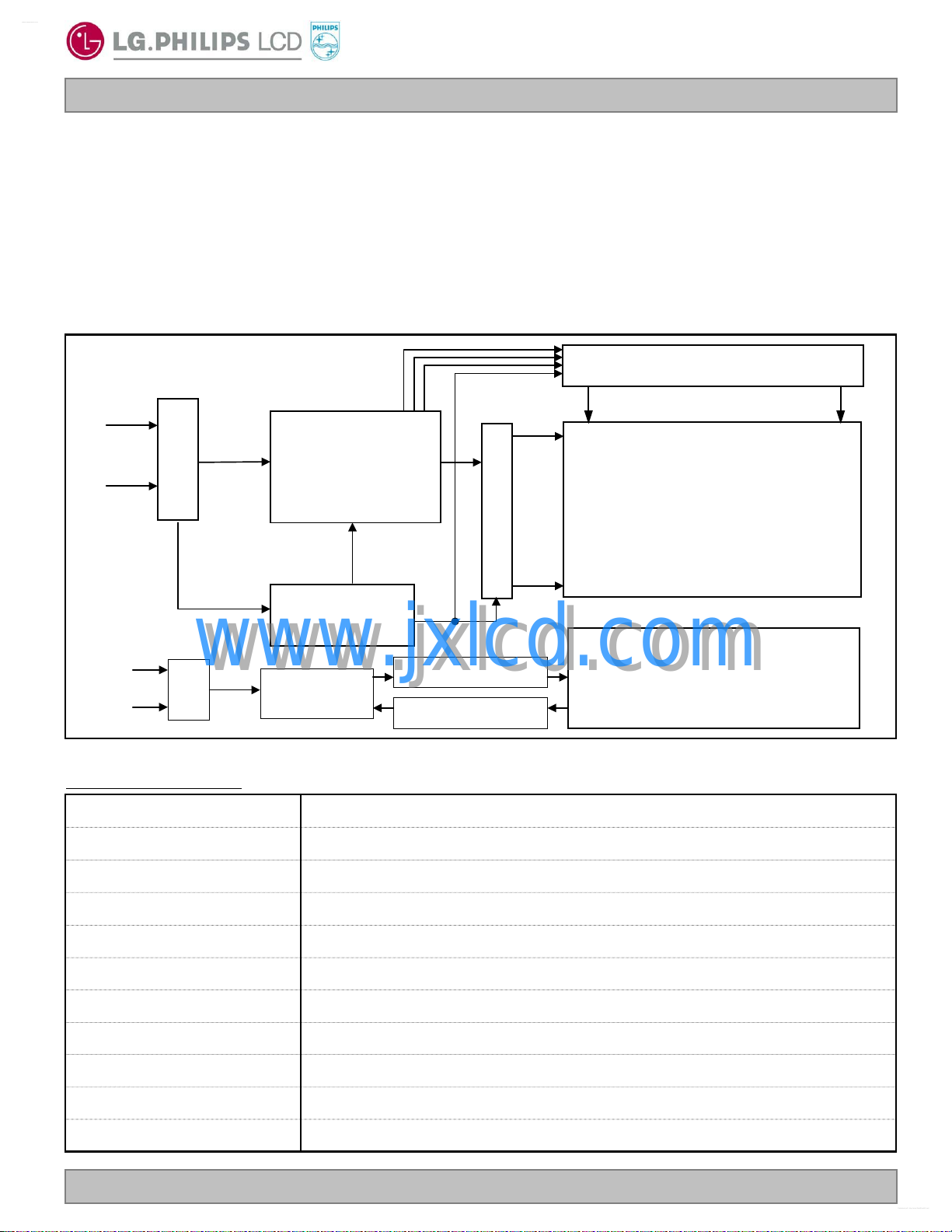
1. General Description
The LM230WU3 LCD is a Color Active Matrix Liquid Crystal Display with an integral Cold Cathode Fluorescent
Lamp(CCFL) back light system. The matrix employs a-Si Thin Film Transistor as the active element. It is a
transmissive type display operating in the normally black mode. This TFT-LCD has a 23.0 inch diagonally
measured active display area with WUXGA resolution(1200 vertical by 1920 horizontal pixel array). Each pixel
is divided into Red, Green and Blue sub-pixels or dots which are arranged in vertical stripes. Gray scale or
the luminance of the sub-pixel color is determined with a 8-bit gray scale signal for each dot, thus, presenting
a palette of more than 16,777,216 colors.
The LM230WU3 has been designed to apply the 2 port LVDS interface.
LVDS
2port
CN1
(30pin)
+18.0V
+18.0V
+24.0V
GND
www.jxlcd.com
www.jxlcd.com
CN2
(14Pin)
General Features
R/G/B
Timing
Controller
Power Circuit
Block
Inverter
Block
23.0 inches(58.4cm) diagonalActive Screen Size
Gate Driver Circuit
2pin x 6CNs (High)
2pin x 1CN (Low)
Source Driver Circuit
S1 S1920
G1
TFT - LCD Panel
(1920 × RGB × 1200 pixels)
G1200
Back light Assembly
(Direct Light Type_12CCFL)
523.4(H) x 335.6(V) x 41.0(D) mm(Typ.)Outline Dimension
0.258 mm x 0.258 mmPixel Pitch
1920 horiz. By 1200 vert. Pixels RGB stripes arrangementPixel Format
8-bit, 16,777,216 colorsColor Depth
2
300 cd/m
View Angle Free (R/L 178(Typ.), U/D 178(Typ.))Viewing Angle(CR>10)
Total 61.5 Watt (Typ.) (7.5 Watt
2,870g(typ.)Weight
Transmissive mode, normally blackDisplay Operating Mode
Hard coating(3H), Anti-glare treatment of the front polarizerSurface Treatment
Ver. 0.0 Nov. 28 . 2005
(Center 1 point)Luminance, White
@VLCD, 54.0 @300cd)Power Consumption
4/ 29
LM230WU3
www.DataSheet.co.kr
Datasheet pdf - http://www.DataSheet4U.net/
Liquid Crystal Display
Product Specification
2. Absolute Maximum Ratings
The following are maximum values which, if exceeded, may cause faulty operation or damage to the unit.
Table 1. ABSOLUTE MAXIMUM RATINGS
Parameter Notes
Power Input Voltage
Operating Temperature
Storage Temperature
Operating Ambient Humidity
Storage Humidity
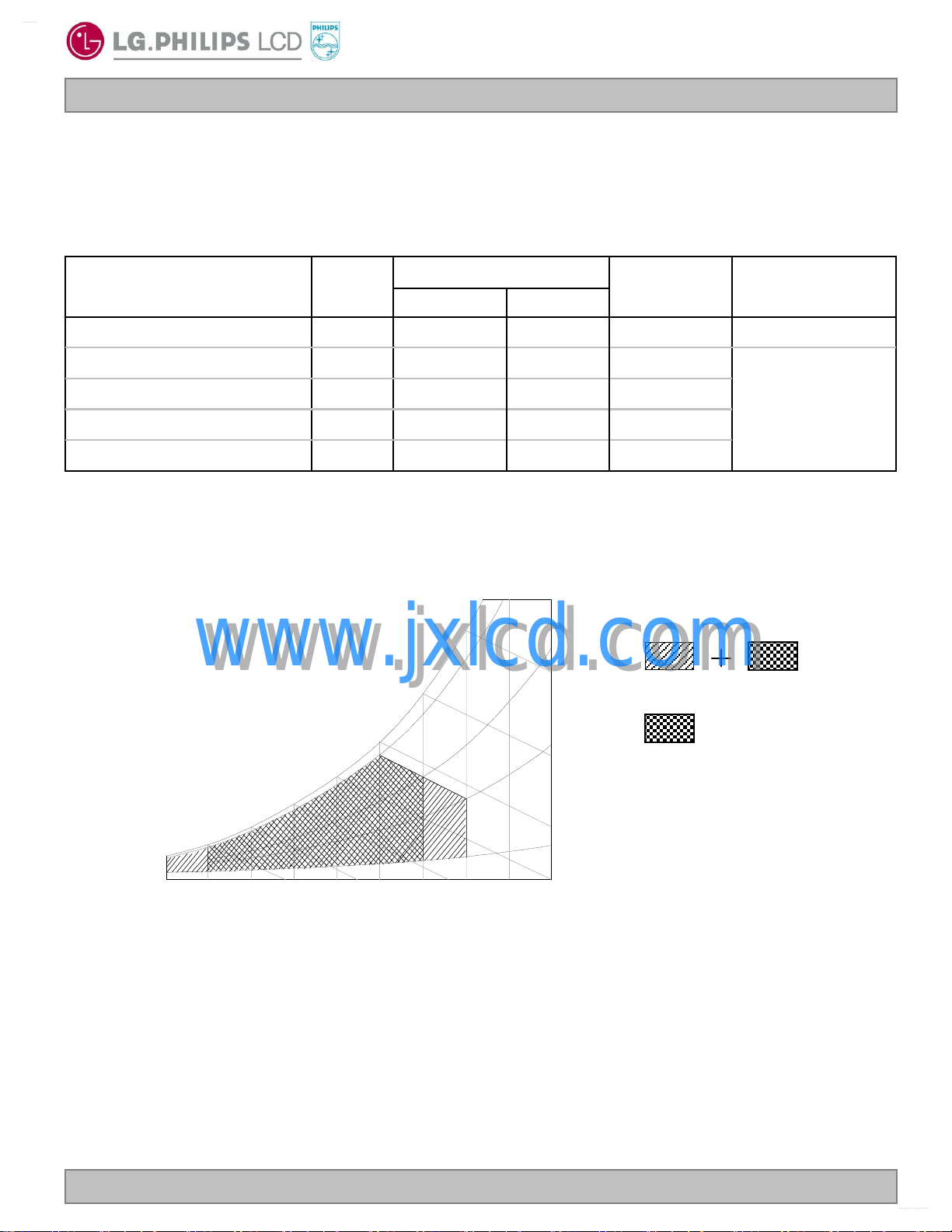
Note : 1. Temperature and relative humidity range are shown in the figure below.
Wet bulb temperature should be 39 °C Max, and no condensation of water.
www.jxlcd.com
www.jxlcd.com
Wet Bulb
Temperature [C]
10
0
Symbol
50
40
30
20
Values
MaxMin
500TOP
60-20TST
90%
60
60%
40%
Humidity [(%)RH]
10%
Units
Vdc21-0.3VLCD
°C
°C
%RH9010HOP
%RH9010HST
at 25 ± 2°C
1
Storage
Operation
10 20 30 40 50 60 70 800-20
Dry Bulb Temperature [C]
Ver. 0.0 Nov. 28 . 2005
5/ 29
LM230WU3
www.DataSheet.co.kr
Datasheet pdf - http://www.DataSheet4U.net/
Liquid Crystal Display
Product Specification
3. Electrical Specifications
3-1. Electrical Characteristics
It requires two power inputs. One is employed to power the LCD electronics and to drive the TFT array and
liquid crystal. The second input power for the CCFL, is typically generated by an inverter. The inverter is an
external unit to the LCDs.
Table 2-1. ELECTRICAL CHARACTERISTICS
Parameter Symbol
MODULE :
ILCDPower Supply Input Current
Note :
1. The specified current and power consumption are under the V
whereas mosaic pattern(8 x 6) is displayed and f
2. The current is specified at the maximum current pattern.
3. The duration of rush current is about 2ms and rising time of power Input is 1ms(min.).
www.jxlcd.com
www.jxlcd.com
White : 255Gray
Black : 0Gray
is the frame frequency.
V
Values
MaxTypMin
=18.0V, 25 ± 2°C,fV=60Hz condition
LCD
Maximum current pattern
Vdc19.018.017.0VLCDPower Supply Input Voltage
mVp-p400VdRFPermissive Power Input Ripple
NotesUnit
1mA470415-
2mA645560-
1Watt8.57.5-PLCDPower Consumption
3A3.0--IRUSHRush current
Mosaic Pattern(8 x 6)
Ver. 0.0 Nov. 28 . 2005
White Pattern
6/ 29
Product Specification
www.DataSheet.co.kr
Datasheet pdf - http://www.DataSheet4U.net/
Table 2-2. INVERTER ELECTRICAL CHARACTERISTICS
ConditionSymbolParameter
Inverter :
Values
LM230WU3
Liquid Crystal Display
Unit
Max.Typ.Min.
Notes
Input Voltage
Input Current
LAMP :
Notes :
1. The input voltage ripple is limited below 400mVp-p.
2.The specified current and power consumption are under the typical supply Input voltage, 24V.
3.The life is determined as the time at which luminance of the lamp is 50% compared to that of initial
value at the typical lamp current on condition of continuous operating at 25 ± 2°C.
4. Electrical characteristics are determined after the unit has been ‘ON’ and stable for approximately
30min in a dark environment at 25 °C± 2°C.
www.jxlcd.com
www.jxlcd.com
ON/OFFB/L on/off control
DDB
DDB
BRBrightness Adj
BR
BR
= 3.3VI
= 3.3VPBInput Power
V26.024.022.0V
A2.62.25-V
Watt5954-V
V5.0-2.0Lamp ON = HighV
V0.8-0.0Lamp OFF =Low
V3.3-0V
1
2
2
3Hrs50,000Life time
Ver. 0.0 Nov. 28 . 2005
7/ 29
LM230WU3
www.DataSheet.co.kr
Datasheet pdf - http://www.DataSheet4U.net/
Liquid Crystal Display
Product Specification
3-2. Interface Connections
This LCD employs Two interface connections, a 30 pin connector is used for the module electronics and a
14Pin Connector is used for the integral backlight system.
3-2-1. LCD Module
- LCD Connector(CN1) : IS100-L30B-C23 (UJU) or Equivalent
- Mating Connector : FI-X30C2L (Manufactured by JAE) or Equivalent
Table 3 MODULE CONNECTOR(CN1) PIN CONFIGURATION
SymbolNo
GND1
GND2
FRX0-3
FRX0+4
FRX1-5
FRX1+6
FRX2-7
FRX2+8
FRXCLK-9
FRXCLK+10
FRX3-11
FRX3+12
SRX0-13
SRX0+14
SRX1-15
Ground
Ground
LVDS Signal of Odd channel 0(-)
LVDS Signal of Odd channel 0(+)
LVDS Signal of Odd channel 1(-)
LVDS Signal of Odd channel 1(+)
LVDS Signal of Odd channel 2(-)
LVDS Signal of Odd channel 2(+)
www.jxlcd.com
www.jxlcd.com
LVDS Signal of Odd channel Clock(-)
LVDS Signal of Odd channel Clock(+)
LVDS Signal of Odd channel 3(-)
LVDS Signal of Odd channel 3(+)
LVDS Signal of Even channel 0(-)
LVDS Signal of Even channel 0(+)
LVDS Signal of Even channel 1(-)
Description
No
16
17
18
19
20
21
22
23
24
25
26
27
28
29
30
Symbol
SRX1+
SRX2-
SRX2+
SRXCLK-
SRXCLK+
SRX3-
SRX3+
GND
GND
GND
VLCD
VLCD
VLCD
NC
NC
Symbol
LVDS Signal of Even channel 1(+)
LVDS Signal of Even channel 2(-)
LVDS Signal of Even channel 2(+)
LVDS Signal of Even channel Clock(-)
LVDS Signal of Even channel Clock(+)
LVDS Signal of Even channel 3(-)
LVDS Signal of Even channel 3(+)
Ground
Ground
Ground
Supply voltage +18.0V
Supply voltage +18.0V
Supply voltage +18.0V
OPEN
OPEN
Notes: 1. All GND(ground) pins should be connected together and should also be connected to the LCD’s
metal frame.
2. All V
(power input) pins should be connected together.
LCD
3. Input Level of LVDS signal is based on the IEA 664 Standard.
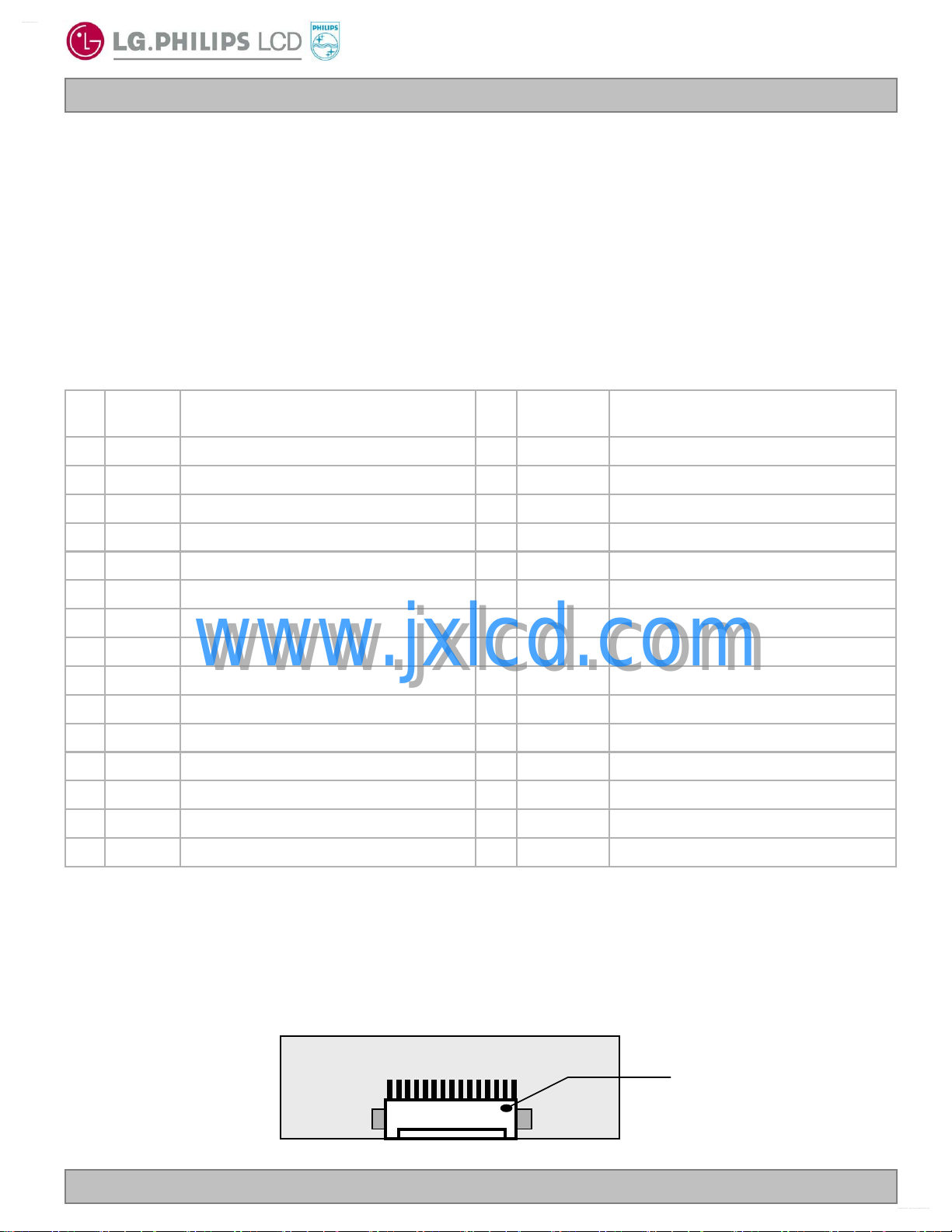
Rear view of LCM
1
Ver. 0.0 Nov. 28 . 2005
30
IS100-L30B-C23(UJU)
8/ 29
LM230WU3
www.DataSheet.co.kr
Datasheet pdf - http://www.DataSheet4U.net/
Liquid Crystal Display
Product Specification
Table 4. REQUIRED SIGNAL ASSIGNMENT FOR Flat Link (TI:SN75LVDS83) Transmitter
Pin # Require SignalPin Name Pin # Require SignalPin Name
1 Power Supply for TTL InputVCC 29 Ground pin for TTLGND
2 TTL Input (R7)D5 30 TTL Input (DE)D26
3 TTL Input (R5)D6 31 TTL Level clock InputTXCLKIN
4 TTL Input (G0)D7 32 Power Down InputPWR DWN
5 Ground pin for TTLGND 33 Ground pin for PLLPLL GND
6 TTL Input (G1)D8 34 Power Supply for PLLPLL VCC
7 TTL Input (G2)D9 35 Ground pin for PLLPLL GND
8 TTL Input (G6)D10 36 Ground pin for LVDSLVDS GND
9 Power Supply for TTL InputVCC 37 Positive LVDS differential data output 3TxOUT3+
10 TTL Input (G7)D11 38 Negative LVDS differential data output 3TxOUT3-
11 TTL Input (G3)D12 39 Positive LVDS differential clock outputTXCLKOUT+
12 TTL Input (G4)D13 40 Negative LVDS differential clock outputTXCLKOUT-
13 Ground pin for TTLGND 41 Positive LVDS differential data output 2TXOUT2+
14 TTL Input (G5)D14 42 Negative LVDS differential data output 2TXOUT2-
www.jxlcd.com
15 TTL Input (B0)D15 43 Ground pin for LVDSLVDS GND
16 TTL Input (B6)D16 44 Power Supply for LVDSLVDS VCC
17 Power Supply for TTL InputVCC 45 Positive LVDS differential data output 1TXOUT1+
19 TTL Input (B1)D18
20 TTL Input (B2)D19
22 TTL Input (B3)D20
23 TTL Input (B4)D21
24 TTL Input (B5)D22
www.jxlcd.com
46 Negative LVDS differential data output 1TXOUT1-18 TTL Input (B7)D17
47 Positive LVDS differential data output 0TXOUT0+
48 Negative LVDS differential data output 0TXOUT0-
49 Ground pin for LVDSLVDS GND21 Ground pin for TTL InputGND
50 TTL Input (R6)D27
51 TTL Input (R0)D0
52 TTL Input (R1)D1
25 TTL Input (RSVD)D23
26 Power Supply for TTL InputVCC 54 TTL Input (R2)D2
Notes : Refer to LVDS Transmitter Data Sheet for detail descriptions.
Ver. 0.0 Nov. 28 . 2005
53 Ground pin for TTLGND
55 TTL Input (R3)D327 TTL Input (HSYNC)D24
56 TTL Input (R4)D428 TTL Input (VSYNC)D25
9/ 29
 Loading...