

(●●●●) Preliminary Specification
( ) Final Specification
LM230WF4
Liquid Crystal Display
Product Specification
SPECIFICATION
FOR
APPROVAL
23” Full HD TFT LCDTitle
BUYER
MODEL
*When you obtain standard approval,
www.jxlcd.com
www.jxlcd.com
APPROVED BY
/
/
/
SIGNATURE
DATE
please use the above model name without suffix
APPROVED BY
G.T. Kim / G.Manager
REVIEWED BY
B.C. Song / Manager
PREPARED BY
H.Y. Kim / Engineer
LG Display Co., Ltd.SUPPLIER
LM230WF4*MODEL
TLA1SUFFIX
SIGNATURE
DATE
Please return 1 copy for your confirmation with
your signature and comments.
Ver. 0.2 Nov. 27. 2009
Products Engineering Dept.
LG. Display Co., Ltd
1 / 34
Product Specification
CONTENTS
LM230WF4
Liquid Crystal Display
ITEMNo
COVER
CONTENTS
RECORD OF REVISIONS
GENERAL DESCRIPTION1
ABSOLUTE MAXIMUM RATINGS2
ELECTRICAL SPECIFICATIONS3
ELECTRICAL CHARACTREISTICS3-1
INTERFACE CONNECTIONS3-2
LVDS CHARACTERISTICS3-3
SIGNAL TIMING SPECIFICATIONS3-4
SIGNAL TIMING WAVEFORMS3-5
COLOR DATA REFERNECE3-6
www.jxlcd.com
www.jxlcd.com
POWER SEQUENCE3-7
OPTICAL SFECIFICATIONS4
Page
1
2
3
4
5
6
6
9
13
17
18
19
20
21
MECHANICAL CHARACTERISTICS5
RELIABLITY6
INTERNATIONAL STANDARDS7
SAFETY7-1
EMC7-2
ENVIRONMENT7-3
PACKING8
DESIGNATION OF LOT MARK8-1
PACKING FORM8-2
PRECAUTIONS9
Ver. 0.2 Nov. 27. 2009
27
30
31
31
31
31
32
32
32
33
2 / 34
Product Specification
RECORD OF REVISIONS
LM230WF4
Liquid Crystal Display
Revision
No
DescriptionPageRevision Date
Preliminary-Nov. 09. 20090.1
Delete Cover shield notch-Nov.25. 20090.2
www.jxlcd.com
www.jxlcd.com
Ver. 0.2 Nov. 27. 2009
3 / 34
LM230WF4
Liquid Crystal Display
Product Specification
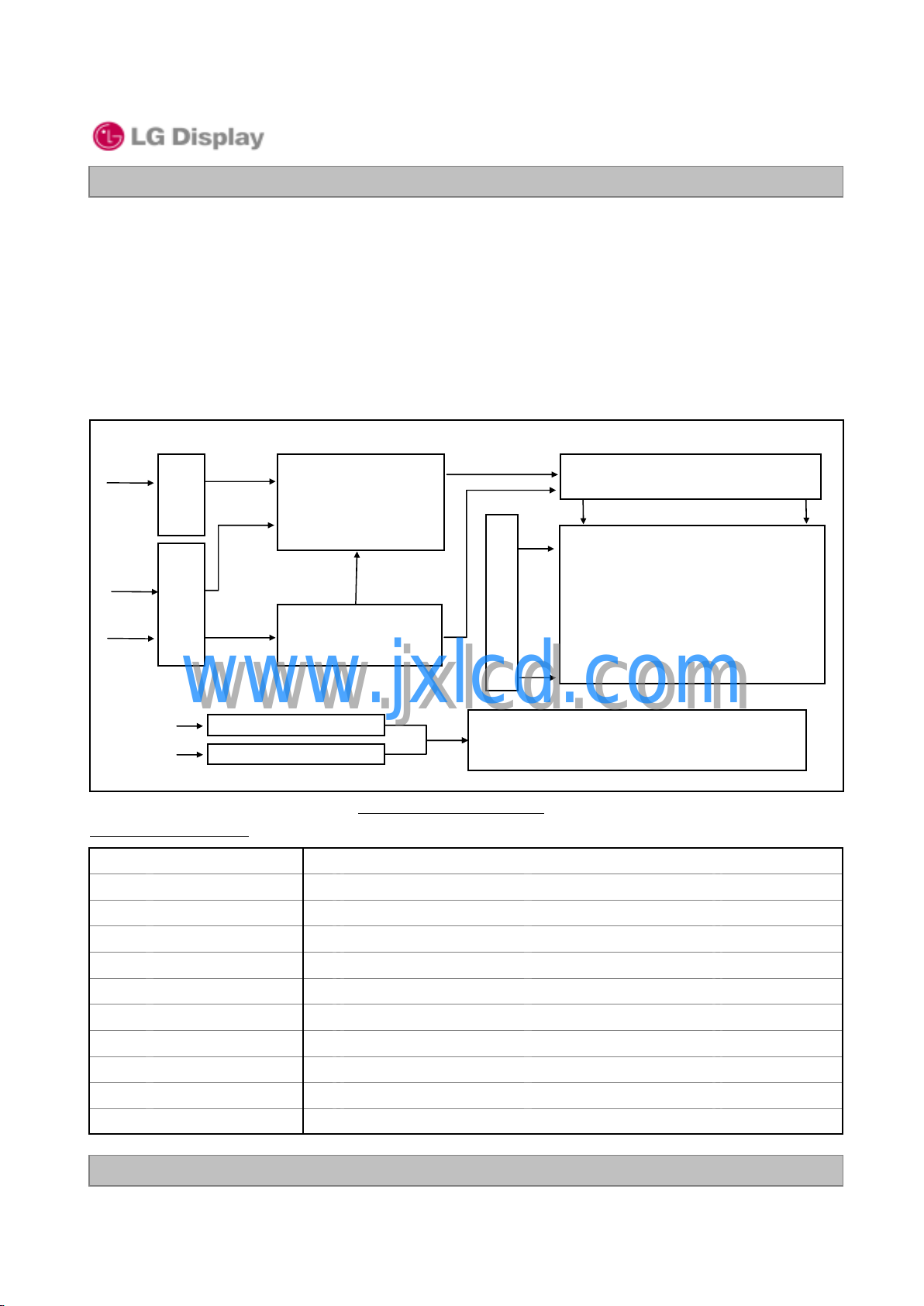
1. General Description
LM230WF4 is a Color Active Matrix Liquid Crystal Display with an integral Cold Cathode Fluorescent Lamp
(CCFL) backlight system. The matrix employs a-Si Thin Film Transistor as the active element.
It is a transmissive type display operating in the normally white mode. It has a 23-inch diagonally measured
active display area with FHD resolution (1080 vertical by 1920 horizontal pixel array). Each pixel is divided into
Red, Green and Blue sub-pixels or dots which are arranged in vertical stripes. Gray scale or the brightness of
the sub-pixel color is determined with a 8-bit gray scale signal for each dot, thus, presenting a palette of more
than 16.7M colors with A-FRC(Advanced Frame Rate Control). It is intended to support displays where high
brightness, super wide viewing angle and high color saturation, etc.
LVDS
2Port
LVDS
2Port
V
LCD
(+12V)
V
Lamp
V
Lamp
LVDS 3,4
CN2
(41pin)
LVDS 1,2
CN1
(51pin)
www.jxlcd.com
www.jxlcd.com
General Features
Power Consumption
Timing Control Block
Power Circuit Block
CN3, 4
CN5, 6
(2Pin)
(2Pin)
23 inches (58.42cm) diagonalActive Screen Size
533.2(H) x 312.0(V) x 20.0(D) mm (Typ.)Outline Dimension
0.0884(H) mm x RGB x 0.2652(V) mmPixel Pitch
1920 horizontal x 1080 vertical Pixels, RGB stripe arrangementPixel Format
16.7M colorsColor Depth
400 cd/m
R/L 170(Typ.), U/D 160(Typ.)Viewing Angle(CR>10)
Total 30.42 W (Typ.) ( 4.92 W @
2,600g (Typ.)Weight
Transmissive mode, Normally WhiteDisplay Operating Mode
Hard coating (3H) & Anti-Glare treatment of the front polarizerSurface Treatment
Mini-LVDS(RGB)
Dual Gate Driver Circuit
G1
G1080
Figure 1. Block Diagram
2
(Center, 1 point)Luminance, White
Source Driver Circuit
S1
TFT - LCD Panel
(1920 × RGB × 1080 pixels)
Backlight Assembly (4 CCFLs)
V
LCD
, 25.50 W @ 400 cd/m2)
S1920
Ver. 0.2 Nov. 27. 2009
4 / 34
Liquid Crystal Display
Product Specification
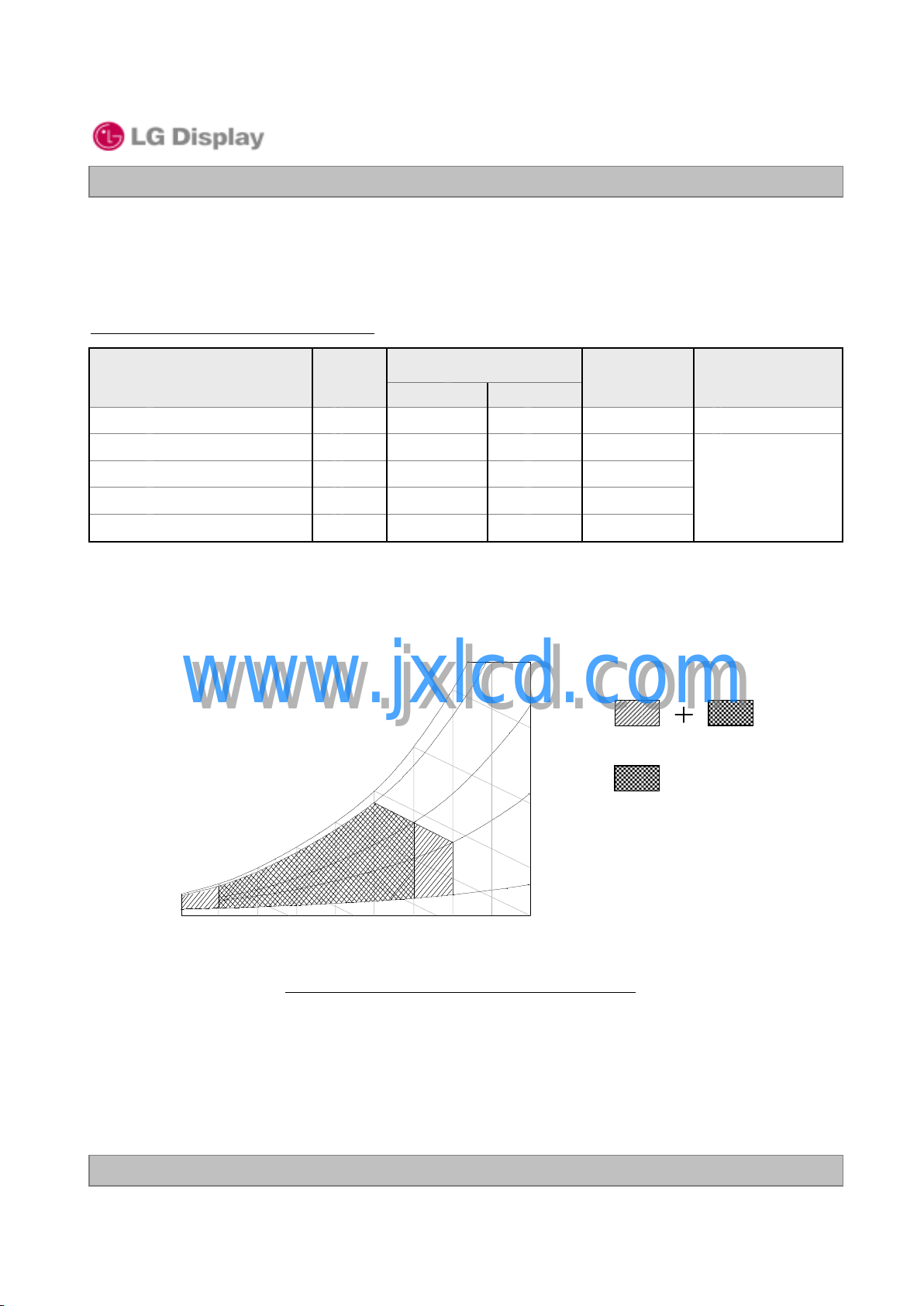
2. Absolute Maximum Ratings
The following are maximum values which, if exceeded, may cause faulty operation or permanent
damage to the unit.
Table 1. Absolute Maximum Ratings
LM230WF4
Parameter Notes
Power Supply Input Voltage
Operating Temperature
Storage Temperature
Operating Ambient Humidity
Storage Humidity
Note : 1. Temperature and relative humidity range are shown in the figure below.
Wet bulb temperature should be 39 °C Max, and no condensation of water.
www.jxlcd.com
www.jxlcd.com
Wet Bulb
Temperature [C]
10
0
Symbol
LCD
OP
ST
OP
ST
50
40
30
20
Values
MaxMin
90%
60
60%
40%
Humidity [(%)RH]
10%
Units
Vdc12.4-0.3V
°C500T
°C60-20T
%RH9010H
%RH9010H
at 25 ± 2°C
1
Storage
Operation
10 20 30 40 50 60 70 800-20
Dry Bulb Temperature [C]
Figure 2. Temperature and Relative Humidity
Ver. 0.2 Nov. 27. 2009
5 / 34
LM230WF4
Liquid Crystal Display
Product Specification
3. Electrical Specifications
3-1. Electrical Characteristics
It requires two power inputs. One is employed to power the LCD electronics and to drive the TFT array
and liquid crystal. The other input power for the CCFL is typically generated by an inverter. The inverter is
an external unit to the LCDs.
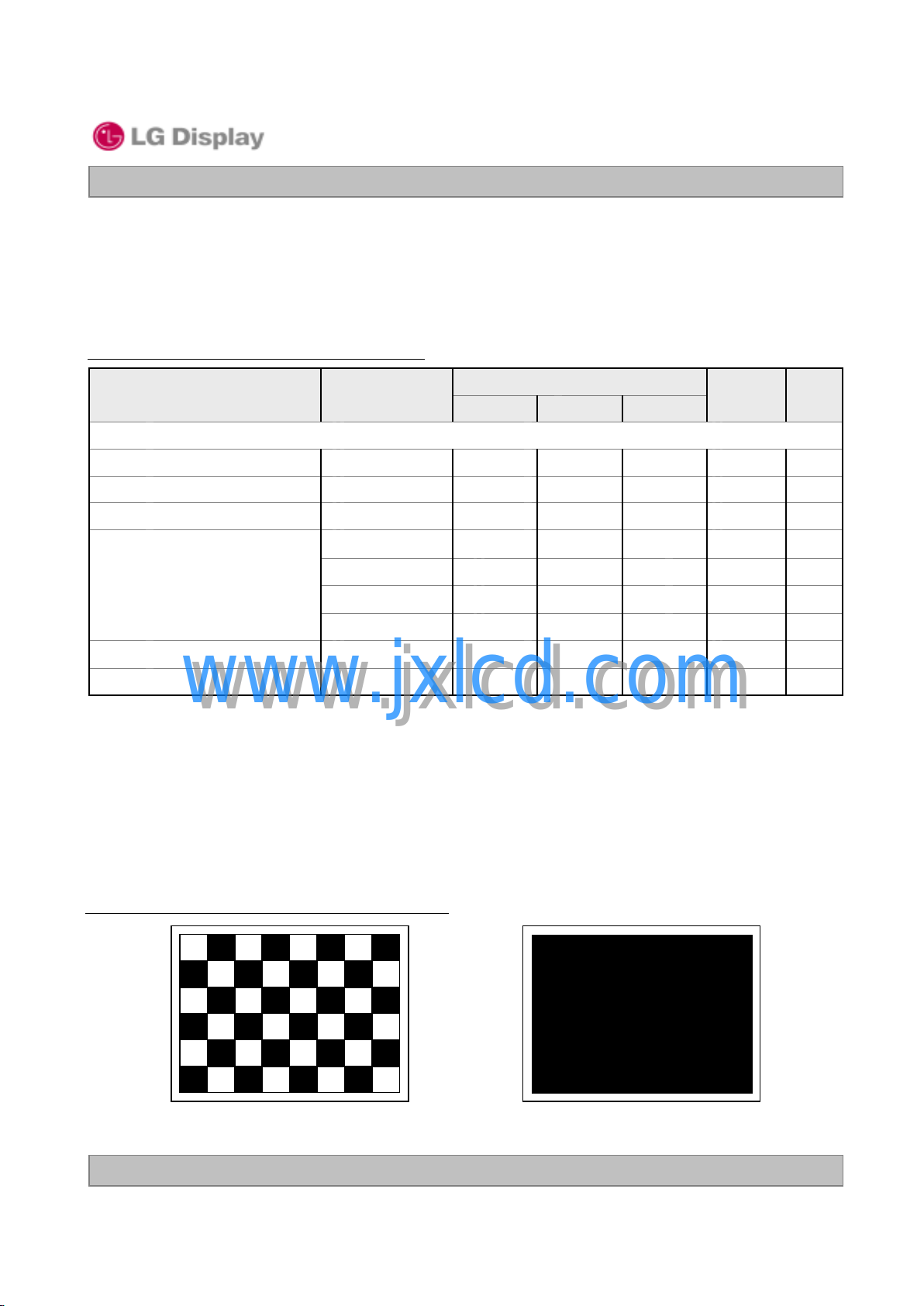
Table 2. Electrical Characteristics (Module)
Parameter Symbol
MODULE :
Power Supply Input Voltage
Permissive Power Input Ripple
Differential Impedance
I
Power Supply Input Current
Power Consumption
Rush current
Note :
1. Permissive power ripple should be measured under V
condition and at that time, we recommend the bandwidth configuration of oscilloscope is to be under 20MHz.
2. The specified current and power consumption are under the V
whereas Mosaic pattern shown in the [ Figure 3. ] is displayed.
3. The specified current is measured at the Full black pattern.
4. The duration of rush current is about 5ms and measured under condition that the rising time of power
input is 500us ± 20%.
www.jxlcd.com
www.jxlcd.com
I
LCD
dRF
m
LCD-MOSAIC_60Hz
LCD-Black_60Hz
LCD-MOSAIC_120Hz
LCD-Black_120Hz
LCD
RUSH
=12.0V, 25±2°C, fV(frame frequency)= 120Hz
LCD
Values
MaxTypMin
Vdc12.412.011.6V
Ohm11010090Z
mA760550I
mA1080680I
=12.0V, 25 ± 2°C, fV= 60Hz condition
LCD
NotesUnit
1mVp-p400V
2mA490410-
3mA580480-
2W12.964.92-P
4A3.0--I
Figure 3. Pattern for Electrical Characteristics
Mosaic Pattern(8 x 6)
White : 255Gray Black : 0Gray
Ver. 0.2 Nov. 27. 2009
Full Black Pattern
6 / 34
Product Specification
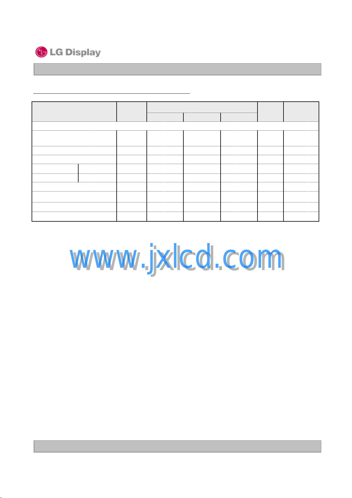
Table 3. Electrical Characteristics (Backlight System)
LM230WF4
Liquid Crystal Display
Parameter Symbol
LAMP :
Operating Voltage
Operating Current
Established Starting Voltage
at 25 °C
at 0 °C
Operating Frequency
Discharge Stabilization Time
Power Consumption
Life Time
Note : The design of the inverter must have specifications for the lamp in LCD Assembly.
The performance of the Lamp in LCM, for example life time or brightness, is extremely influenced by
the characteristics of the DC-AC inverter. So all the parameters of an inverter should be carefully
designed so as not to produce too much leakage current from high-voltage output of the inverter.
When you design or order the inverter, please make sure unwanted lighting caused by the mismatch
www.jxlcd.com
of the lamp and the inverter (no lighting, flicker, etc) never occurs. When you confirm it, the LCD Assembly should be operated in the same condition as installed in you instrument.
※ Do not attach a conducting tape to lamp connecting wire.
If the lamp wire attach to a conducting tape, TFT-LCD Module has a low luminance and the inverter
has abnormal action. Because leakage current is occurred between lamp wire and conducting tape.
1. Specified values are for a single lamp.
2. Operating voltage is measured at 25 ± 2°C. The variance of the voltage is ± 10%.
3. The voltage above VSshould be applied to the lamps for more than 1 second for start-up.
(Inverter open voltage must be more than lamp starting voltage.)
Otherwise, the lamps may not be turned on. The used lamp current is the lamp typical current.
4. Lamp frequency may produce interface with horizontal synchronous frequency and as a result this may
cause beat on the display. Therefore lamp frequency shall be as far as possible from the horizontal
synchronous frequency and from its harmonics in order to prevent interference.
5. Let’s define the brightness of the lamp after being lighted for 5 minutes as 100%.
TSis the time required for the brightness of the center of the lamp to be not less than 95%.
6. The lamp power consumption shown above does not include loss of external inverter.
The used lamp current is the lamp typical current. (PBL= VBLx IBLx N
7. The life time is determined as the time at which brightness of the lamp is 50% compared to that of initial
value at the typical lamp current on condition of continuous operating at 25 ± 2°C.
www.jxlcd.com
V
BL
I
BL
S
f
BL
T
S
P
BL
830
(8.0mA)
50,000
Values
850
(7.5mA)
MaxTypMin
1,000
(3.0mA)
8.07.53.0
1,500
1,800
706040
3
28.125.5
)
LAMP
NotesUnit
RMS
RMS
V
RMS
V
RMS
1, 2V
1mA
1, 3V
4kHz
1, 5min
6W
1, 7Hrs
Ver. 0.2 Nov. 27. 2009
7 / 34
LM230WF4
Liquid Crystal Display
Product Specification
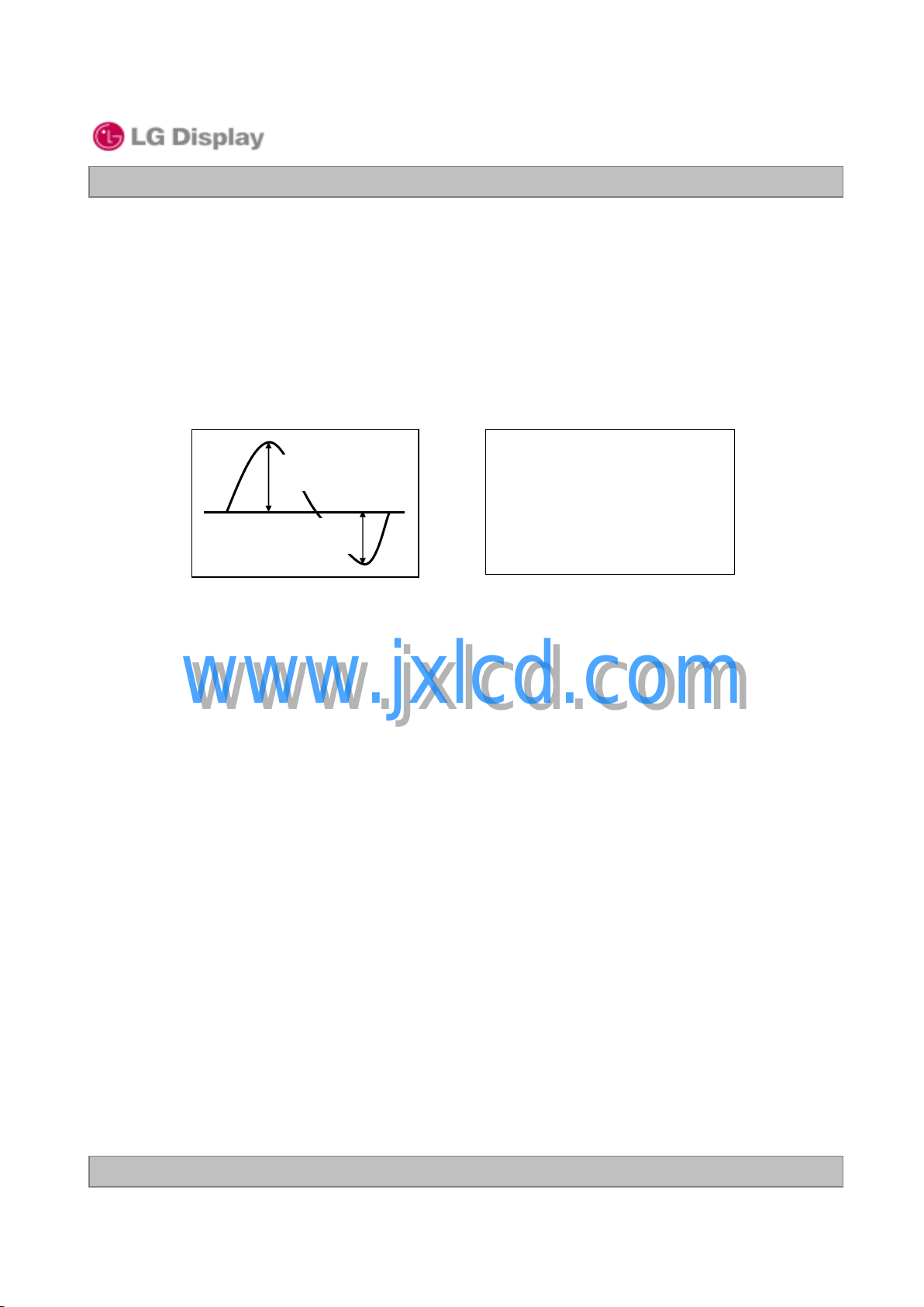
8. The output of the inverter must have symmetrical(negative and positive) voltage waveform and
symmetrical current waveform (Unsymmetrical ratio is less than 10%). Please do not use the inverter
which has unsymmetrical voltage and unsymmetrical current and spike wave.
Requirements for a system inverter design, which is intended to have a better display performance, a
better power efficiency and a more reliable lamp, are following.
It shall help increase the lamp lifetime and reduce leakage current.
a. The asymmetry rate of the inverter waveform should be less than 10%.
b. The distortion rate of the waveform should be within √2 ±10%.
* Inverter output waveform had better be more similar to ideal sine wave.
* Asymmetry rate:
I
p
| I p– I –p| / I
rms
x 100%
I
-p
9. The inverter which is combined with this LCM, is highly recommended to connect coupling(ballast)
condenser at the high voltage output side. When you use the inverter which has not coupling(ballast)
condenser, it may cause abnormal lamp lighting because of biased mercury as time goes.
10.In case of edge type backlight with over 4 parallel lamps, input current and voltage waveform should
be synchronized
www.jxlcd.com
www.jxlcd.com
* Distortion rate
I p(or I –p) / I
rms
Ver. 0.2 Nov. 27. 2009
8 / 34
LM230WF4
Liquid Crystal Display
Product Specification
3-2. Interface Connections
This LCD module employs two kinds of interface connection, 51 pin connector and 41 pin connector are
used for the module electronics.
3-2-1. LCD Module
Table 4. Module Connector (CN1) Pin Configuration
- LCD Connector(CN1): IS050-C51B-C39-A(manufactured by UJU) or compatible
- Mating Connector : FI-R51HL(JAE) or compatible
No Symbol Description No Symbol Description
1 GND Ground 27 NC No Connection (BIT)
2 MST MST Option Enable 28 R2AN 2nd LVDS Channel Signal (A-)
3 PWM_OUT PWM Signal Output 29 R2AP 2nd LVDS Channel Signal (A+)
4 NC No Connection (SDA) 30 R2BN 2nd LVDS Channel Signal (B-)
5 NC No Connection (SCL) 31 R2BP 2nd LVDS Channel Signal (B+)
6 NC No Connection 32 R2CN 2nd LVDS Channel Signal (C-)
7 NC No Connection (DISM) 33 R2CP 2nd LVDS Channel Signal (C+)
8 NC No Connection 34 GND Ground
9 ODC_EN ODC Enable 35 R2CLKN 2nd LVDS Channel Clock Signal(-)
10 FPS_DET H: High Frame rate, L: Legacy 36 R2CLKP 2nd LVDS Channel Clock Signal(+)
11 GND Ground 37 GND Ground
12 R1AN 1st LVDS Channel Signal (A-) 38 R2DN 2nd LVDS Channel Signal (D-)
13 R1AP 1st LVDS Channel Signal (A+) 39 R2DP 2nd LVDS Channel Signal (D+)
14 R1BN 1st LVDS Channel Signal (B-) 40 GND Ground
15 R1BP 1st LVDS Channel Signal (B+) 41 NC No connection
16 R1CN 1st LVDS Channel Signal (C-) 42 NC No connection
17 R1CP 1st LVDS Channel Signal (C+) 43 GND Ground
18 GND Ground 44 GND Ground (AGP)
19 R1CLKN 1st LVDS Channel Clock Signal(-) 45 GND Ground
20 R1CLKP 1st LVDS Channel Clock Signal(+) 46 NC No connection
21 GND Ground 47 NC No connection
22 R1DN 1st LVDS Channel Signal (D-) 48 VLCD Power Supply +12.0V
23 R1DP 1st LVDS Channel Signal (D+) 49 VLCD Power Supply +12.0V
24 GND Ground 50 VLCD Power Supply +12.0V
25 NC No Connection 51 VLCD Power Supply +12.0V
26 NC No Connection
www.jxlcd.com
www.jxlcd.com
Ver. 0.2 Nov. 27. 2009
9 / 34
Liquid Crystal Display
Product Specification
Table 5. Module Connector (CN2) Pin Configuration
- LCD Connector(CN2): IS050-C41B-C39-A(manufactured by UJU) or compatible
- Mating Connector : FI-RE41HL(JAE) or compatible
No Symbol Description No Symbol Description
1 NC No connection 22 GND Ground
2 NC No connection 23 NC No connection
3 NC No connection 24 NC No connection
4 NC No connection 25 GND Ground
5 NC No connection 26 RA4N 4th LVDS Channel Signal (A-)
6 NC No connection 27 RA4P 4th LVDS Channel Signal (A+)
7 NC No connection 28 RB4N 4th LVDS Channel Signal (B-)
8 NC No connection 29 RB4P 4th LVDS Channel Signal (B+)
9 GND Ground 30 RC4N 4th LVDS Channel Signal (C-)
10 RA3N 3rd LVDS Channel Signal (A-) 31 RC4P 4th LVDS Channel Signal (C+)
LM230WF4
11 RA3P 3rd LVDS Channel Signal (A+) 32 GND Ground
12 RB3N 3rd LVDS Channel Signal (B-) 33 RCLK4N 4th LVDS Channel Clock Signal(-)
13 RB3P 3rd LVDS Channel Signal (B+) 34 RCLK4P 4th LVDS Channel Clock Signal(+)
14 RC3N 3rd LVDS Channel Signal (C-) 35 GND Ground
15 RC3P 3rd LVDS Channel Signal (C+) 36 RD4N 4th LVDS Channel Signal (D-)
16 GND Ground 37 RD4P 4th LVDS Channel Signal (D+)
17 RCLK3N 3rd LVDS Channel Clock Signal(-) 38 GND Ground
18 RCLK3P 3rd LVDS Channel Clock Signal(+) 39 NC No connection
19 GND Ground 40 GND Ground
20 RD3N 3rd LVDS Channel Signal (D-) 41 GND Ground
21 RD3P 3rd LVDS Channel Signal (D+)
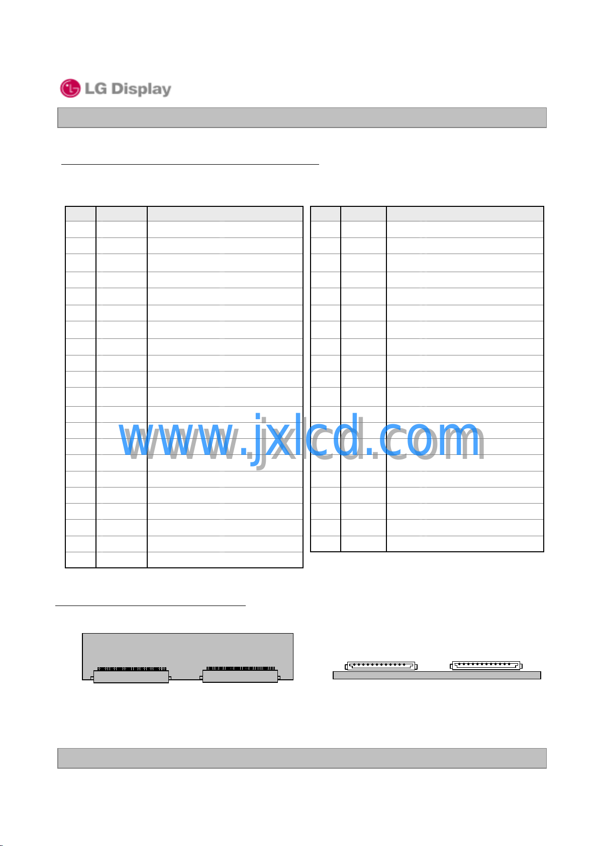
Figure 4. Module Connector Diagram
www.jxlcd.com
www.jxlcd.com
#1
CN1 CN2
#51 #1 #41
#1 #51
#1 #41
[Rear view of LCM]
Ver. 0.2 Nov. 27. 2009
10 / 34

LM230WF4
Liquid Crystal Display
Product Specification
Note :
1. All GND (Ground) pins should be connected together to the LCD module’s metal frame.
2. All V
3. All Input levels of LVDS signals are based on the EIA 664 Standard.
4. Always all LVDS signal and clock input should be 4 channels and synchronized.
5. Specific pins (CN1 pin No. 4~8, 27, 44) are used for internal process of the LCD module manufacturing.
Leave these pins in condition that ‘No Connection’.
6. MST : MST option enable (Input), ‘L’ : Disable, ‘H’ : Enable
7. PWM_OUT : Reference signal (Output) for synchronizing Vsync and Burst frequency of inverter to avoid
8. ODC_EN : ODC enable (Input), ‘L’ : Disable, ‘H’ : Enable
9. FPS_DET : Frame rate detection (Input), ‘L’ : Under 50MHz, ‘H’: Over 50MHz.
(power input) pins should be connected together.
LCD
MST option : Left side image is applied to CN1, 1st& 2ndLVDS channel.
Right side image is applied to CN2, 3rd& 4thLVDS channel.
It should be tided up ‘L’ or ‘H’.
wavy noise, flickering, etc.
It should be tided up ‘L’ or ‘H’.
www.jxlcd.com
www.jxlcd.com
Ver. 0.2 Nov. 27. 2009
11 / 34
 Loading...