

LG LM-230WF1-TLA5 Service manual
Product Specification
LM230WF1
Liquid Crystal Display
www.jxlcd.com
www.jxlcd.com
Ver. 1.0 D
ec. 21, 2009
Product Specification
Contents
LM230WF1
Liquid Crystal Display
No ITEM
COVER 1
CONTENTS 2
RECORD OF REVISIONS 3
1 GENERAL DESCRIPTION 4
2 ABSOLUTE MAXIMUM RATINGS 5
3 ELECTRICAL SPECIFICATIONS 6
1) ELECTRICAL CHARACTERISTICS 6
2) INTERFACE CONNECTIONS 9
3) LVDS characteristics 12
4) SIGNAL TIMING SPECIFICATIONS 15
5) SIGNAL TIMING WAVEFORMS 16
6) COLOR INPUT DATA REFERNECE 17
7) POWER SEQUENCE 18
8) POWER DIP CONDITION 19
4 OPTICAL SPECIFICATIONS 20
5 MECHANICAL CHARACTERISTICS 25
www.jxlcd.com
www.jxlcd.com
Page
6 RELIABILITY 28
7 INTERNATIONAL STANDARDS 29
1) SAFETY
2) EMC
8 PACKING 30
1) DESIGNATION OF LOT MARK 30
2) PACKING FORM 30
9 PRECAUTIONS 31
1) MOUNTING PRECAUTIONS 31
2) OPERATING PRECAUTIONS 31
3) ELECTROSTATIC DISCHARGE CONTROL 32
4) PRECAUTIONS FOR STRONG LIGHT EXPOSURE 32
5) STROAGE 32
6) HANDLING PRECAUTIONS FOR PROTECTION FILM 32
Ver. 1.0 D
ec. 21, 2009
29
29
2 / 32
Product Specification
Record of revisions
Revision No DescriptionDate Page
LM230WF1
Liquid Crystal Display
Ver. 0.1
Ver. 1.0
Feb. 26, 2009
Dec. 21, 2009 9, 10
26
www.jxlcd.com
www.jxlcd.com
Preliminary Specifications.
Change the Maker name of Interface Connector.
(LSC →LSM)
Add the Position of Source D-IC in Rear View Drawing.
Final Specifications.
Ver. 1.0 D
ec. 21, 2009
3 / 32
LM230WF1
Liquid Crystal Display
Product Specification
1. General description
LM230WF1-TLA5 is a Color Active Matrix Liquid Crystal Display with an integral Cold Cathode Fluorescent
amp(CCFL) backlight system. The matrix employs a-Si Thin Film Transistor as the active element. It is a
L
transmissive type display operating in the normally white mode. It has a 23 inch diagonally measured active
display area with FHD resolution (1080 vertical by 1920 horizontal pixel array) Each pixel is divided into Red,
Green and Blue sub-pixels or dots which are arranged in vertical stripes. Gray scale or the brightness of the
sub-pixel color is determined with a 8-bit gray scale signal for each dot, thus, presenting a palette of more than
16,7M colors with Advanced-FRC(Frame Rate Control). It has been designed to apply the interface method
that enables low power, high speed, low EMI. FPD Link or compatible must be used as a LVDS(Low Voltage
Differential Signaling) chip. It is intended to support applications where thin thickness, wide viewing angle, low
power are critical factors and graphic displays are important. In combination with the vertical arrangement of
the sub-pixels, the LM230WF1-TLA5 characteristics provide an excellent flat panel display for office automation
products such as monitors.
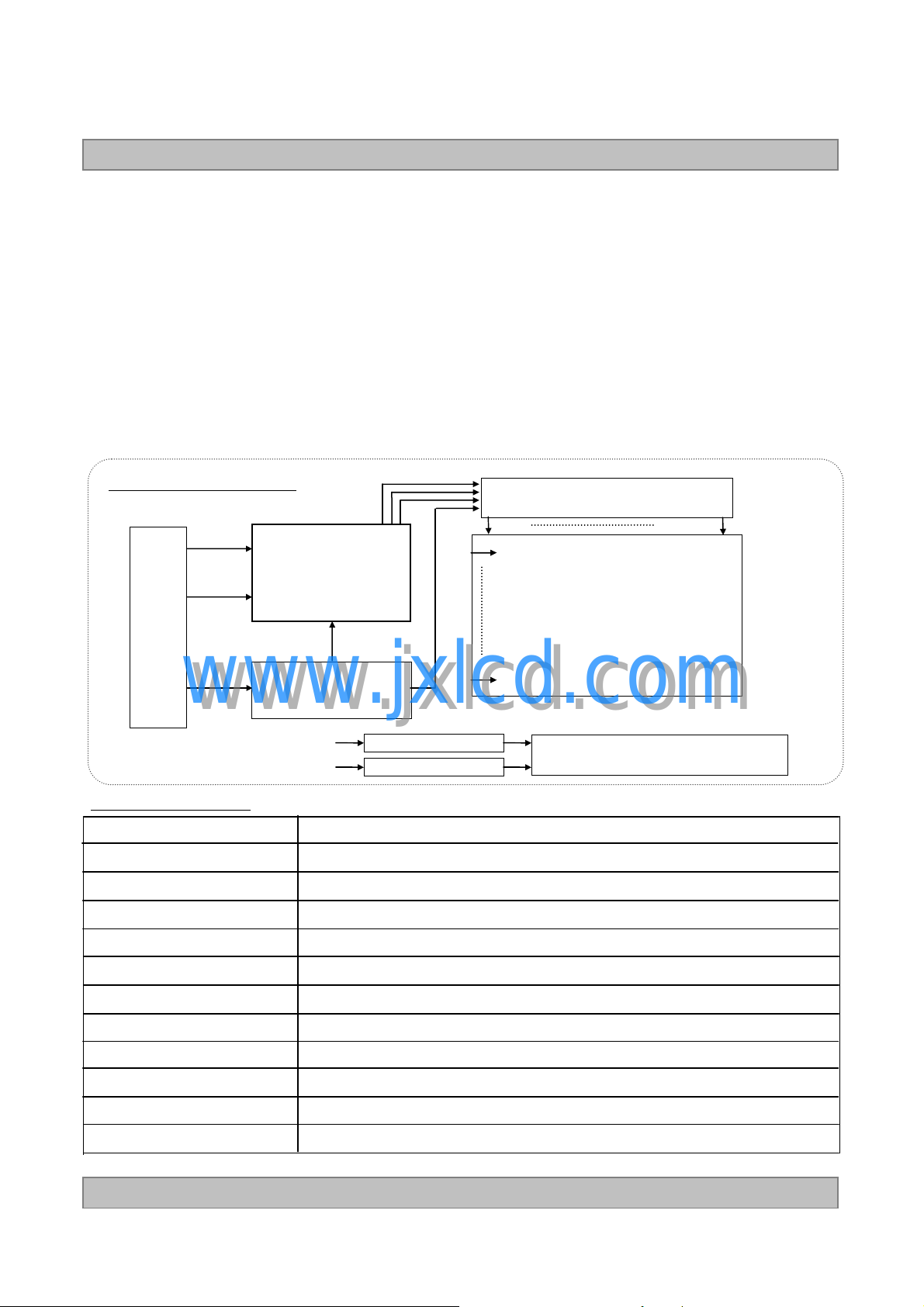
FIG. 1 Block diagram
LVDS
pair #1
LVDS
pair #2
CN1
(30pin)
+5V
LCD
V
www.jxlcd.com
www.jxlcd.com
Power circuit
Timing
controller
block
V
Lamp
V
Lamp
RGB
CN2, 3 (2pin)
CN4, 5 (2pin)
Source driver circuit
S
1
G1
TFT-LCD Panel
(1920× RGB× 1080 pixels)
G1080
Backlight assembly (4 CCFLs)
General features
Active screen size 23 inches(58.42cm) diagonal(Aspect ratio 16:9)
Outline Dimension 533.2(H) x 312.0(V) x 16.5(D) mm(Typ.)
Pixel Pitch 0.265 mm x 0.265 mm
Pixel Format 1920 horiz. By 1080 vert. Pixels RGB stripes arrangement
S1920
Interface LVDS 2Port
Color depth 16.7M colors
Luminance, white 300 cd/m2 ( Center 1Point, typ)
Viewing Angle (CR>10) R/L 170(Typ.), U/D 160(Typ.)
wer Consumption
Po
Weight 2600g(typ.)
Display operating mode Transmissive mode, normally White
Surface treatments Hard coating(3H) & Anti-Glare treatment of the front polarizer
Ver. 1.0 D
Total 30W (Typ.), (4.5W@V
ec. 21, 2009
, 25.5W@IBL=7.5mA)
LCD
4 / 32
Product Specification
2. Absolute maximum ratings
The following are maximum values which, if exceeded,
may cause faulty operation or damage to the unit.
Table 1. Absolute maximum ratings
LM230WF1
Liquid Crystal Display
Parameter Symbol
Power Supply Input Voltage V
Operating Temperature T
Storage Temperature T
Operating Ambient Humidity H
Storage Humidity H
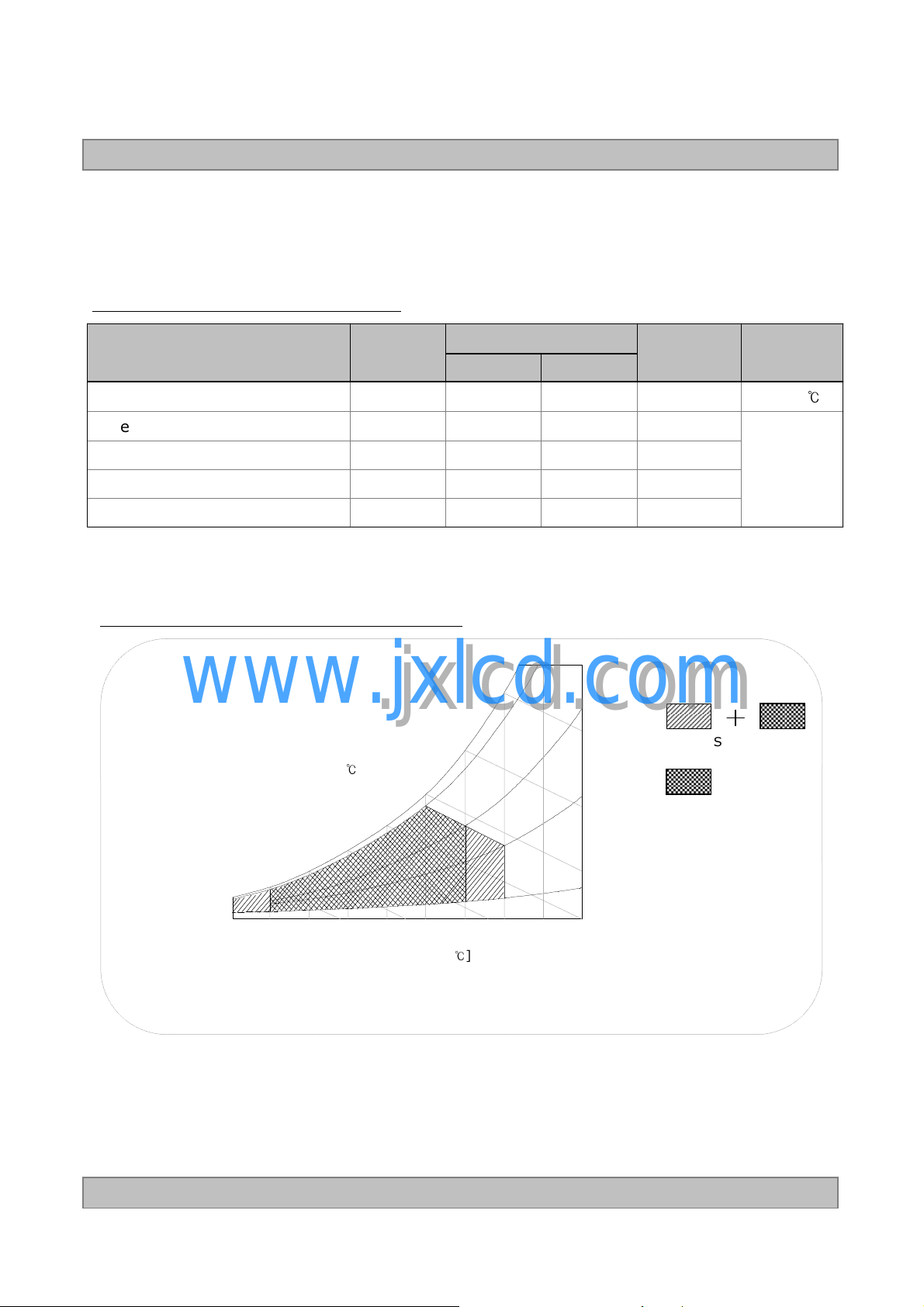
Note : 1. Temperature and relative humidity range are shown in the figure below.
Wet bulb temperature should be 39 °C Max, and no condensation of water.
FIG. 2 Temperature and relative humidity
www.jxlcd.com
www.jxlcd.com
Wet Bulb
Temperature [℃]
20
10
0
LCD
OP
ST
OP
ST
50
40
30
Values
Min Max
-0.3 +6.0 Vdc At 25
0 50 °C
-20 60 °C
10 90 %RH
10 90 %RH
90%
60
60%
40%
10%
Units Notes
Storage
Operation
Humidity
[(%)RH]
℃
1
10 20 30 40 50 60 70 800-20
Dry Bulb Temperature [
Ver. 1.0 D
℃
]
ec. 21, 2009
5 / 32
LM230WF1
Liquid Crystal Display
Product Specification
3. Electrical specifications
-1. Electrical characteristics
3
It requires two power inputs. One is employed to power the LCD electronics and to drive the
FT array and liquid crystal. The second input power for the CCFL/Backlight, is typically
T
generated by an inverter. The inverter is an external unit to the LCDs.
Table 2. Electrical characteristics
Parameter Symbol
MODULE :
Power Supply Input Voltage V
Permissive Power Input Ripple V
Power Supply Input Current
Power Consumption P
Inrush current I
Note :
1. The specified current and power consumption are
under the VLCD=5.0V, 25 ± 2°C,fV=60Hz condition
whereas mosaic pattern(8 x 6) is displayed and fVis the frame frequency.
2. The current is specified at the maximum current pattern.
3. Permissive power ripple should be measured under VCC=5.0V, 25°C, fV(frame frequency)=Max
condition and At that time, we recommend the bandwidth configuration of oscilloscope
is to be under 20MHz.
4. The duration of rush current is about 2ms and rising time of power Input is 500us ± 20%.
FIG.3 pattern for Electrical characteristics
www.jxlcd.com
www.jxlcd.com
LCD
LCD
I
LCD-MOSAIC
I
LCD-BLACK
LCD
RUSH
Min Typ Max
4.5 5.0 5.5 Vdc
- - 0.4 V 3
- 900 1100 mA 1
- 1050 1250 mA 2
- 4.5 5.5 Watt 1
- - 3.0 A 4
Values
Unit Notes
power consumption measurement
White : 255Gray
Black : 0Gray
Mosaic Pattern(8 x 6)
Ver. 1.0 D
ec. 21, 2009
power input ripple
Full Black Pattern
6 / 32
Product Specification
Table 3. Electrical characteristics
LM230WF1
Liquid Crystal Display
Parameter Symbol
LAMP :
Operating Voltage V
Operating Current I
Established Starting Voltage Vs 1, 3
at 25 °C
at 0 °C
Operating Frequency f
Discharge Stabilization Time T
Power Consumption P
Life Time
Note :
The design of the inverter must have specifications for the lamp in LCD Assembly.
The performance of the Lamp in LCM, for example life time or brightness, is extremely influenced
by the characteristics of the DC-AC inverter. So all the parameters of an inverter should be carefully
designed so as not to produce too much leakage current from high-voltage output of the inverter.
When you design or order the inverter, please make sure unwanted lighting caused by the mismatch of
the lamp and the inverter (no lighting, flicker, etc) never occurs. When you confirm it, the LCD–Assembly
should be operated in the same condition as installed in you instrument.
www.jxlcd.com
www.jxlcd.com
BL
BL
BL
S
BL
Min Typ Max
830(8.0mA) 850 (7.5mA) 1000 (3.0mA)
3.0 7.5 8.0
40 6
50000
Values
1500
1800
0 70
25.5 28.1
Unit Notes
V
RMS
mA
RMS
V
RMS
V
RMS
kHz 4
3
Min 1, 5
Watt 6
Hrs 1, 7
1, 2
1
※
Do not attach a conducting tape to lamp connecting wire. If the lamp wire attach to a conducting tape,
TFT-LCD Module has a low luminance and the inverter has abnormal action.
Because leakage current is occurred between lamp wire and conducting tape.
1. Specified values are for a single lamp.
It is only reference voltage in LCM or System.
2. Operating voltage is measured at 25 ± 2°C and follows as below condition,
1) ± 10%@typical operating voltage is based on single lamp.
2) ± 20%@typical operating voltage is based on system & test equipment tolerance.
3. The voltage above VSshould be applied to the lamps for more than 1 second for start-up.
(
Inverter open voltage must be more than lamp starting voltage.)
Otherwise, the lamps may not be turned on. The used lamp current is the lamp typical current.
4. Lamp frequency may produce interface with horizontal synchronous frequency and as a result
this may cause beat on the display. Therefore lamp frequency shall be as away possible from
the horizontal synchronous frequency and from its harmonics in order to prevent interference.
5. Let’s define the brightness of the lamp after being lighted for 5 minutes as 100%.
TSis the time required for the brightness of the center of the lamp to be not less than 95%.
6
. The lamp power consumption shown above does not include loss of external inverter.
The used lamp current is the lamp typical current. (PBL= VBLx IBLx N
7. The life is determined as the time at which brightness of the lamp is 50% compared to that
of initial value at the typical lamp current on condition of continuous operating at 25 ± 2°C.
Ver. 1.0 D
ec. 21, 2009
Lamp
)
7 / 32
Liquid Crystal Display
Product Specification
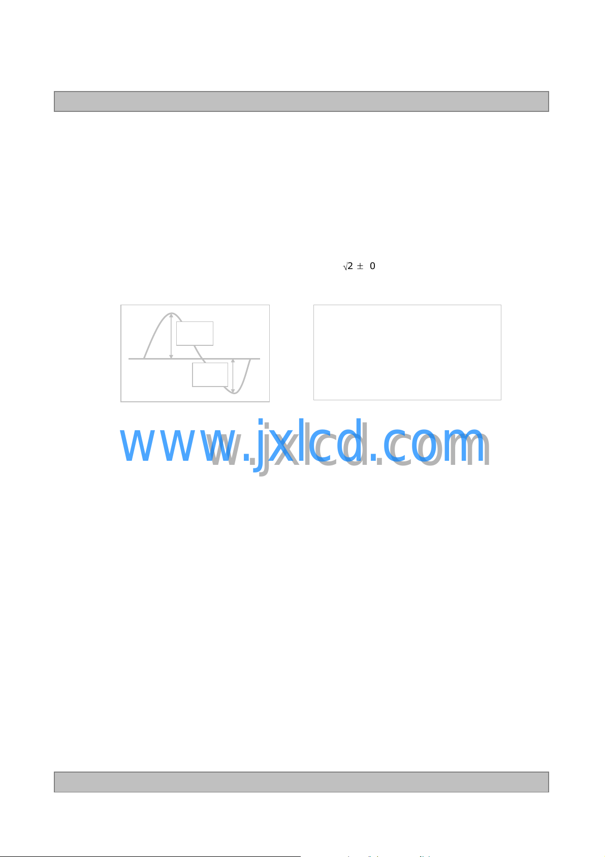
Note :
8
. The output of the inverter must have symmetrical(negative and positive) voltage
waveform and symmetrical current waveform (Unsymmetrical ratio is less than 10%).
Please do not use the inverter which has unsymmetrical voltage and unsymmetrical
current and spike wave. Requirements for a system inverter design, which is intended to
have a better display performance, a better power efficiency and a more reliable lamp,
are following.It shall help increase the lamp lifetime and reduce leakage current.
a. The asymmetry rate of the inverter waveform should be less than 10%.
√2 ±
b. The distortion rate of the waveform should be within
* Inverter output waveform had better be more similar to ideal sine wave.
* Asymmetry rate:
I p
10%.
| I p– I –p| / I
rms
x 100%
LM230WF1
I -p
9. The inverter which is combined with this LCM, is highly recommended to connect
coupling(ballast) condenser at the high voltage output side. When you use the inverter
which has not coupling(ballast) condenser, it may cause abnormal lamp lighting because
of biased mercury as time goes.
10.In case of edgy type back light with over 4 parallel lamps, input current and voltage
wave form should be synchronized
www.jxlcd.com
www.jxlcd.com
* Distortion rate
I p(or I –p) / I
rms
Ver. 1.0 D
ec. 21, 2009
8 / 32
Product Specification
3-2. Interface connections
LCD connector(CN1) : GT103-30S-H23 (LSM) , IS100-L30B-C23 (UJU)
Mating connector : FI-X30H and FI-X30HL (JAE) or Equivalent
Table 4. Module connector(CN1) pin configuration
LM230WF1
Liquid Crystal Display
Pin No
1
2
3
4
5
6
7
8
9
10
11
12
13
14
15
16
17
18
19
20
21
22
23
24
25
26
27
28
29
30
Symbol Description
RXO0RXO0+
RXO1RXO1+
RXO2RXO2+
GND
RXOCRXOC+
RXO3RXO3+
RXE0-
www.jxlcd.com
www.jxlcd.com
RXE0+
GND
RXE1RXE1+
GND
RXE2RXE2+
RXECRXEC+
RXE3RXE3+
GND
NC
NC
NC
VLCD
VLCD
VLCD
Minus signal of 1st channel 0 (LVDS)
Plus signal of 1st channel 0 (LVDS)
Minus signal of 1st channel 1 (LVDS)
Plus signal of 1st channel 1 (LVDS)
Minus signal of 1st channel 2 (LVDS)
Plus signal of 1st channel 2 (LVDS)
Ground
Minus signal of 1st clock channel (LVDS)
Plus signal of 1st clock channel (LVDS)
Minus signal of 1st channel 3 (LVDS)
Plus signal of 1st channel 3 (LVDS)
Minus signal of 2nd channel 0 (LVDS)
Plus signal of 2nd channel 0 (LVDS)
Ground
Minus signal of 2nd channel 1 (LVDS)
Plus signal of 2nd channel 1 (LVDS)
Ground
Minus signal of 2nd channel 2 (LVDS)
Plus signal of 2nd channel 2 (LVDS)
Minus signal of 2nd clock channel (LVDS)
Plus signal of 2nd clock channel (LVDS)
Minus signal of 2nd channel 3 (LVDS)
Plus signal of 2nd channel 3 (LVDS)
Ground
No Connection (For LCD internal use only.)
No Connection (For LCD internal use only.)
No Connection (For LCD internal use only.)
Power Supply (5.0V)
Power Supply (5.0V)
Power Supply (5.0V)
First Pixel data
S
econd Pixel data
Ver. 1.0 D
ec. 21, 2009
9 / 32
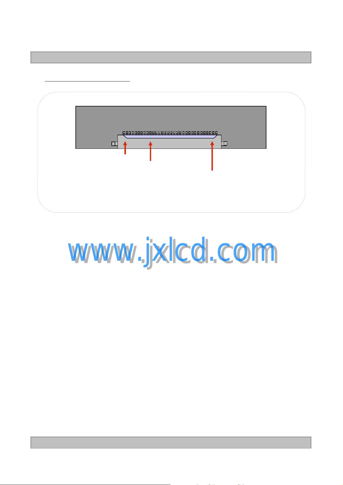
FIG. 4 Connector diagram
#1 #30
1’st signal pairs
LM230WF1
Liquid Crystal Display
Product Specification
GT103-30S-H23 (LSM)
2’nd signal pairs
Power(+5V)
Rear view of LCM
Note:
1. NC: No Connection.
2. All GND(ground) pins should be connected together and to Vss which should also
be connected to the LCD’s metal frame.
www.jxlcd.com
3. All V
4. Input Level of LVDS signal is based on the IEA 664 Standard.
(power input) pins should be connected together.
www.jxlcd.com
LCD
Ver. 1.0 D
ec. 21, 2009
10 / 32
 Loading...