

LG LM-220WE1-TLD3 Service manual
SPECIFICATION
www.DataSheet.co.kr
Datasheet pdf - http://www.DataSheet4U.net/
(◆) Preliminary Specification
( ) Final Spec ific at i on
LM220WE1
Liquid Crystal Display
Product Specification
FOR
APPROVAL
Title
BUYER
MODEL
www.jxlcd.com
www.jxlcd.com
SIGNATURE DATE
/
/
22” WSXGA+ TFT LCD
SUPPLIER LG.Philips LCD CO., Ltd.
*MODEL
SUFFIX TLD3
*When you obtain standard approval,
please use the above model name without suffix
APPROVED BY
K.G. Park / G.Manager
REVIEWED BY
S.J. So / Manager [C]
S.Y. An / Manager [M]
H.S. Lee / Manager [P]
LM220WE1
DATE
/
Please return 1 copy for your confirmation
With your signature and comments.
Ver. 0.1 Jun. 13. 2007
PREPARED BY
J.H. Ji / Engineer
Product Engineering Dept.
LG. Philips LCD Co., Ltd
1/ 31
Product Specification
www.DataSheet.co.kr
Datasheet pdf - http://www.DataSheet4U.net/
Contents
LM220WE1
Liquid Crystal Display
PageITEMNo
COVER
CONTENTS
GENERAL DESCRIPTION1
ABSOLUTE MAXIMUM RATINGS2
ELECTRICAL SPECIFICATIONS3
ELECTRICAL CHARACTREISTICS3-1
INTERFACE CONNECTIONS3-2
SIGNAL TIMING SPECIFICATIONS3-3
SIGNAL TIMING WAVEFORMS3-4
COLOR INPUT DATA REFERNECE3-5
POWER DIP CONDITION3-6
V
www.jxlcd.com
LCD
www.jxlcd.com
POWER SEQUENCE3-7
OPTICAL SFECIFICATIONS4
MECHANICAL CHARACTERISTICS5
1
2
3RECORD OF REVISIONS
4
5
6
6
9
15
16
17
18
19
20
24
RELIABILITY6
INTERNATIONAL STANDARDS7
SAFETY7-1
EMC7-2
PACKING8
DESIGNATION OF LOT MARK8-1
PACKING FORM8-2
Ver. 0.1 Jun. 13. 2007
27
28
28
28
29
29
29
30PRECAUTIONS9
2/ 31
Product Specification
www.DataSheet.co.kr
Datasheet pdf - http://www.DataSheet4U.net/
RECORD OF REVISIONS
Preliminary Specification of LM220WE1-TLD3.-Jun. 13. 20070.1
LM220WE1
Liquid Crystal Display
DESCRIPTIONPageRevision DateRevision No
www.jxlcd.com
www.jxlcd.com
Ver. 0.1 Jun. 13. 2007
3/ 31
LM220WE1
www.DataSheet.co.kr
Datasheet pdf - http://www.DataSheet4U.net/
Liquid Crystal Display
Product Specification
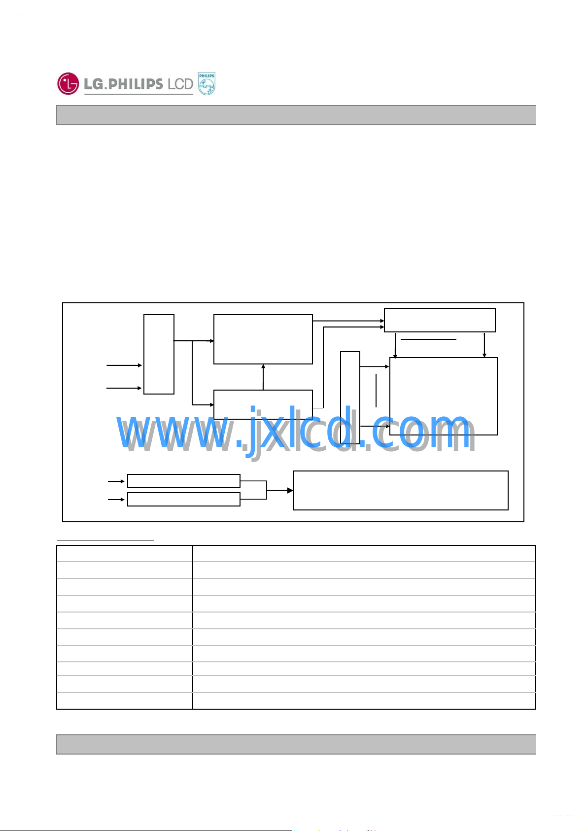
1. General Description
LM220WE1 is a Color Active Matrix Liquid Crystal Display with an integral Cold Cathode Fluorescent
Lamp(CCFL) backlight system. The matrix employs a-Si Thin Film Transistor as the active element.
It is a transmissive type display operating in the normally White mode. It has a 22 inch diagonally measured
active display area with WSXGA+ resolution (1050 vertical by 1680 horizontal pixel array)
Each pixel is divided into Red, Green and Blue sub-pixels or dots which are arranged in vertical stripes.
Gray scale or the brightness of the sub-pixel color is determined wi th a 8-bit gray scale signal for each dot,
thus, presenting a palette of more than 16,7M colors with A-FRC(Advanced Frame Rate Control).
It has been designed to apply the 8Bit 2 port LVDS interface.
It is intended to support displays where high brightness, super wide viewing angle,
high color saturation, and high color are important.
RGB, Dclk, DE
Hsync, Vsync
(LVDS 2 port)
(+5V)
V
LCD
www.jxlcd.com
www.jxlcd.com
V
Lamp
V
Lamp
General Features
CN1
(30pin)
CN2, 3(2PIN)
CN4, 5(2PIN)
Timing Control
Block
Power Circuit Block
21.995 inches(558.673mm) diagonal (Aspect ratio 16:10)Active Screen Size
493.7(H) x 320.1 (V) x 16.5(D) mm (Typ.)Outline Dimension
0.282mm x 0.282mmPixel Pitch
1680 horiz. By 1050 vert. Pixels RGB strip arrangementPixel Format
16,7 M colorsColor Depth
300 cd/m2 (Center 1 point, Typ.)Luminance, White
Total 29.25 Watt(Typ.) (4.370 Watt@VLCD, 24.88 Watt@300cd/[LAMP=7.5mA])Power Consumption
2800 g (Typ.)Weight
Transmissive mode, Normally WhiteDisplay Operating Mode
Hard coating(3H) & Anti-glare treatment of the front polarizerSurface Treatment
Source Driver Circuit
S1680S1
Gate Driver circuit
G1
TFT-LCD Panel
(1680 × 1050 pixels)
G1050
Backlight Assembly(4 CCFL)
Ver. 0.1 Jun. 13. 2007
4/ 31
LM220WE1
www.DataSheet.co.kr
Datasheet pdf - http://www.DataSheet4U.net/
Liquid Crystal Display
Product Specification
2. Absolute Maximum Ratings
The following are maximum values which, if exceeded, may cause faulty operation or damage to the unit.
Table 1. ABSOLUTE MAXIMUM RATINGS
Parameter Notes
Power Input Voltage
Operating Temperature
Storage Temperature
Operating Ambient Humidity
Storage Humidity
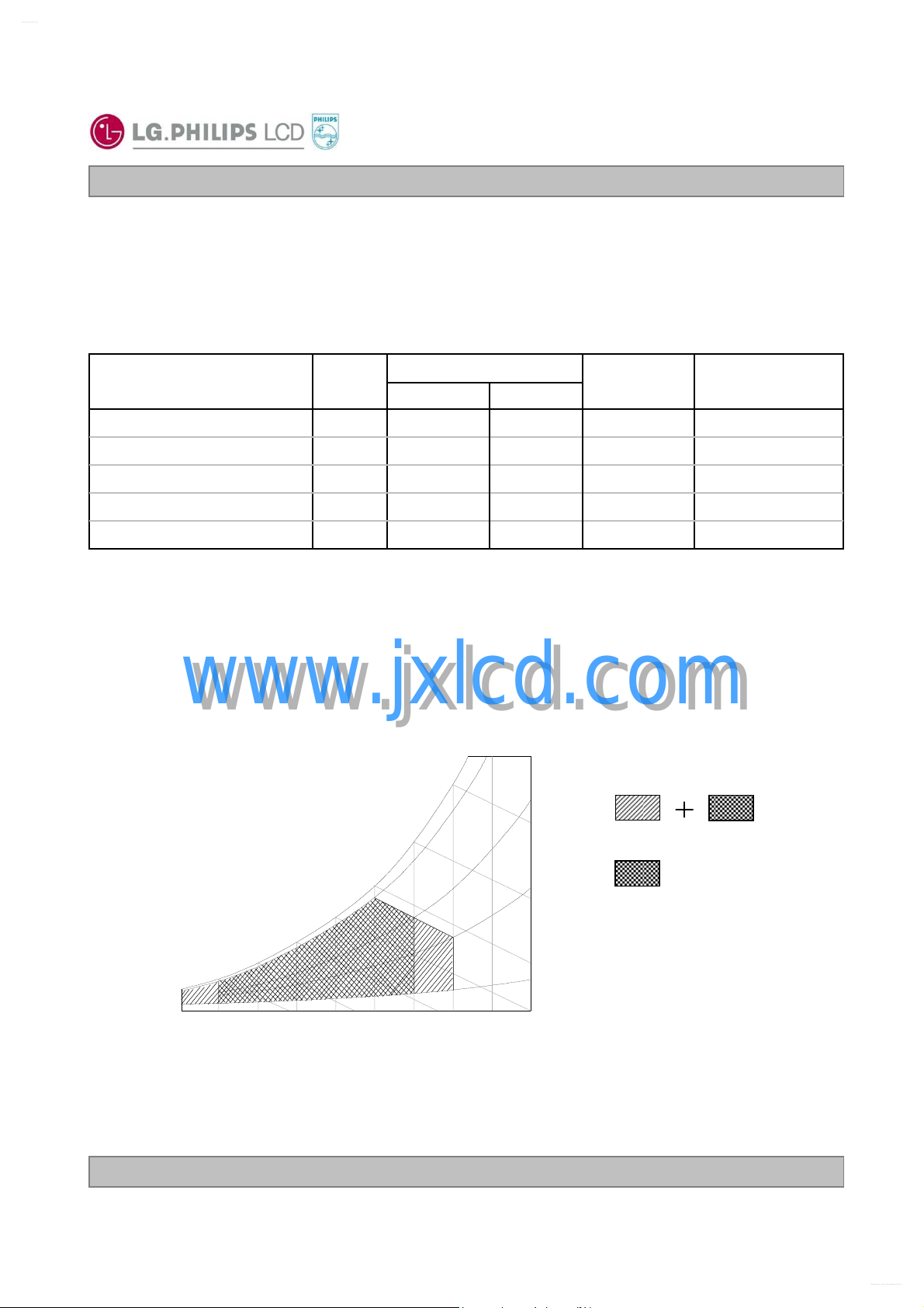
Note : 1. Temperature and relative humidity range are shown in the figure below.
Wet bulb temperature should be 39 °C Max, and no condensation of water.
www.jxlcd.com
www.jxlcd.com
Symbol
Values
MaxMin
+5.5-0.3VLCD
500TOP
60-20TST
90%
60
60%
Units
°C
°C
DC
at 25 ± 2 °CV
1
1
1%RH9010HOP
1%RH9010HST
Wet Bulb
50
Temperature [C]
40
30
20
10
0
10 20 30 40 50 60 70 800-20
Dry Bulb Temperature [C]
Ver. 0.1 Jun. 13. 2007
40%
10%
Storage
Operation
Humidity [(%)RH]
5/ 31
LM220WE1
www.DataSheet.co.kr
Datasheet pdf - http://www.DataSheet4U.net/
Liquid Crystal Display
Product Specification
3. Electrical Specifications
3-1. Electrical Characteristics
It requires two power inputs. One is employed to power the LCD electronics and to drive the TFT array and
liquid crystal. The second input power for the CCFL, is typically generated by an inverter. The inverter is an
external unit to the LCDs.
Table 2_1. ELECTRICAL CHARACTERISTICS
Parameter Symbol
MODULE :
ILCDPower Supply Input Current
Note :
1. The specified current and power consumption are under the V
whereas mosaic pattern(8 x 6) is displayed and f
2. The current is specified at the maximum current pattern.
3. The duration of rush current is about 2ms and rising time of power Input is 500us ± 20%.(min.).
White : 255Gray
Black : 0Gray
www.jxlcd.com
www.jxlcd.com
is the frame frequency.
V
Maximum current pattern
Values
MaxTypMin
Vdc5.55.04.5VLCDPower Supply Input Voltage
=5.0V, 25 ± 2°C,fV=60Hz condition
LCD
NotesUnit
1mA10058742mA142210941Watt5.0254.370-PLCDPower Consumption
3A3--IRUSHRush current
Mosaic Pattern(8 x 6)
Ver. 0.1 Jun. 13. 2007
Black Pattern
6/ 31
Product Specification
www.DataSheet.co.kr
Datasheet pdf - http://www.DataSheet4U.net/
Table 2_2. ELECTRICAL CHARACTERISTICS
LM220WE1
Liquid Crystal Display
Parameter Symbol
LAMP :
at 25 °C
at 0 °C
Operating Frequency
Discharge Stabilization Time
Power Consumption
Life Time
Note : The design of the inverter must have specifications for the lamp in LCD Assembly.
The performance of the Lamp in LCM, for e xample life time or brightness, is e xtremely influenced by
the characteristics of the DC-AC inverter. So all the parameters of an inverter should be carefully
designed so as not to produce too much leakage current from high-voltage output of the inverter.
When you design or order the inverter, please make sure unwanted lighting caused by the mismatch
www.jxlcd.com
of the lamp and the inverter (no lighting, flicker, etc) ne ver occurs. When you confirm it, the LCD–
Assembly should be operated in the same condition as installed in you instrument.
※ Do not attach a conducting tape to lamp connecting wire.
If the lamp wire attach to a conducting tape, TFT-LCD Module has a low luminance and the inverter
has abnormal action. Because leakage current is occurred between lamp wire and conducting tape.
www.jxlcd.com
Values
MaxTypMin
1000830810VBLOperating Voltage
8.07.53.0IBLOperating Current
1250
1550
RMS
RMS
V
RMS
V
RMS
NotesUnit
1, 2V
1mA
1, 3VsEstablished Starting Voltage
4kHz806040fBL
1, 5Min3Ts
6W27.424.9PBL
1, 7Hrs50,000
1. Specified values are for a single lamp.
2. Operating voltage is measured at 25 ± 2°C. The variance of the voltage is ± 10%.
3. The voltage above V
(Inverter open voltage must be more than lamp starting voltage.)
Otherwise, the lamps may not be turned on. The used lamp current is the lamp typical current.
4. Lamp frequency may produce interface with horizonta l synchronous frequency and as a result this may
cause beat on the display. Therefore lamp frequency shall be as away possible from the horizontal
synchronous frequency and from its harmonics in order to prevent interference.
5. Let’s define the brightness of the lamp after being lighted for 5 minutes as 100%.
T
is the time required for the brightness of the center of the lamp to be not less than 95%.
S
6. The lamp power consumption shown above does not include loss of external inverter.
The used lamp current is the lamp typical current. (P
7. The life is determined as the time at which brightness of the lamp is 50% compared to that of initial
value at the typical lamp current on condition of continuous operating at 25 ± 2°C.
Ver. 0.1 Jun. 13. 2007
should be applied to the lamps for more than 1 second for start-up.
S
= VBLx IBLx N
BL
Lamp
)
7/ 31
LM220WE1
www.DataSheet.co.kr
Datasheet pdf - http://www.DataSheet4U.net/
Liquid Crystal Display
Product Specification
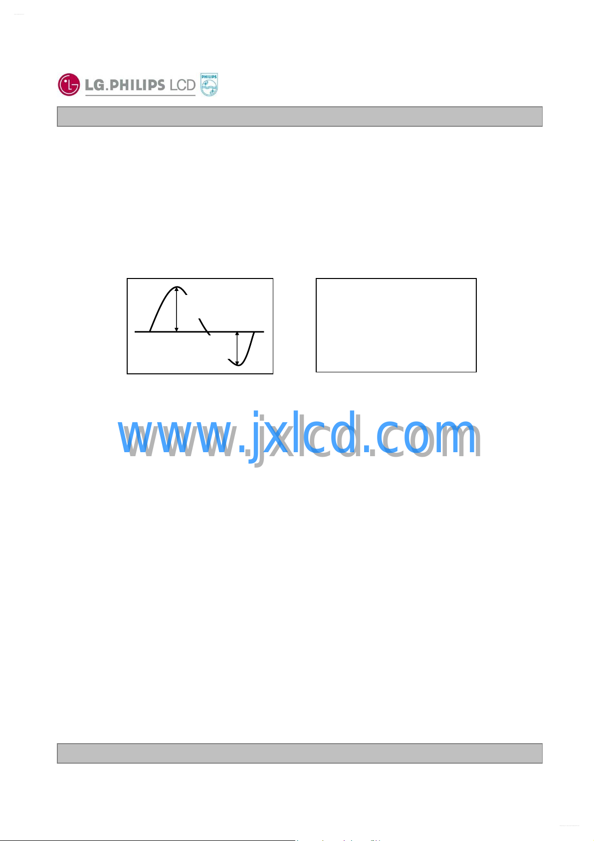
8. The output of the inverter must have symmetrical(negative and positive) voltage waveform and
symmetrical current waveform (Unsymmetrical ratio is less than 10%). Please do not use the inverter
which has unsymmetrical voltage and unsymmetrical current and spike wave.
Requirements for a system inverter design, which is intended to have a better display performance, a
better power efficiency and a more reliable lamp, are following.
It shall help increase the lamp lifetime and reduce leakage current.
a. The asymmetry rate of the inverter waveform should be less than 10%.
b. The distortion rate of the waveform should be within √2 ±10%.
* Inverter output waveform had better be more similar to ideal sine wave.
* Asymmetry rate:
I p
| I
p
–I –p| / I
rms
x 100%
I -p
9. The inverter which is combined with this LCM, is highly recommended to connect coupling(ballast)
condenser at the high voltage output side. When you use the inverter which has not coupling(ballast)
condenser, it may cause abnormal lamp lighting because of biased mercury as time goes.
10.In case of edgy type back light with over 4 parallel lamps, input current and voltage wave form should
be synchronized
www.jxlcd.com
www.jxlcd.com
* Distortion rate
I
(or I –p) / I
p
rms
Ver. 0.1 Jun. 13. 2007
8/ 31
LM220WE1
www.DataSheet.co.kr
Datasheet pdf - http://www.DataSheet4U.net/
Liquid Crystal Display
Product Specification
3-2. Interface Connections
Interface chip must be used LVDS, part No. SN75LVDS83 (Tx, Texas Instrument) or compatible.
This LCD employs a interface connection, a 30 pin connector is used for the module electronics interface.
Four 2pin connectors are used for the integral backlight system. The electronics interface connector is
a model MDF76LBRW-30S-1H manufactured by HIROSE or FI-XB30SRL-HF11 manufactured by JAE.
The pin configuration for the connector is shown in the table 3 and the signal mapping with LVDS transmitter
is shown in the table 4.
Table 3. MODULE CONNECTOR(CN1) PIN CONFIGURATION
Pin No
1
2
3
4
5
6
7
8
9
10
11
12
13
14
15
16
17
18
19
20
21
22
23
24
25
26
27
28
29
30
Symbol Description
RxO0RxO0+
RxO1RxO1+
RxO2RxO2+
GND
RxOCRxOC+
RxO3RxO3+
www.jxlcd.com
www.jxlcd.com
RxE0RxE0+
GND
RxE1RxE1+
GND
RxE2RxE2+
RxECRxEC+
RxE3RxE3+
GND
NC
NC
PWM_OUT
VCC
VCC
VCC
Minus signal of odd channel 0 (LVDS)
Plus signal of odd channel 0 (LVDS)
Minus signal of odd channel 1 (LVDS)
Plus signal of odd channel 1 (LVDS)
Minus signal of odd channel 2 (LVDS)
Plus signal of odd channel 2 (LVDS)
Ground
Minus signal of odd clock channel (LVDS)
Plus signal of odd clock channel (LVDS)
Minus signal of odd channel 3 (LVDS)
Plus signal of odd channel 3 (LVDS)
Minus signal of even channel 0 (LVDS)
Plus signal of even channel 0 (LVDS)
Ground
Minus signal of even channel 1 (LVDS)
Plus signal of even channel 1 (LVDS)
Ground
Minus signal of even channel 2 (LVDS)
Plus signal of even channel 2 (LVDS)
Minus signal of even clock channel (LVDS)
Plus signal of even clock channel (LVDS)
Minus signal of even channel 3 (LVDS)
Plus signal of even channel 3 (LVDS)
Ground
No Connection
No Connection
PWM_OUT signal for control burst frequency of Inverter
Power Supply +5.0V
Power Supply +5.0V
Power Supply +5.0V
First Pixel data
Second Pixel data
Ver. 0.1 Jun. 13. 2007
9/ 31
Product Specification
www.DataSheet.co.kr
Datasheet pdf - http://www.DataSheet4U.net/
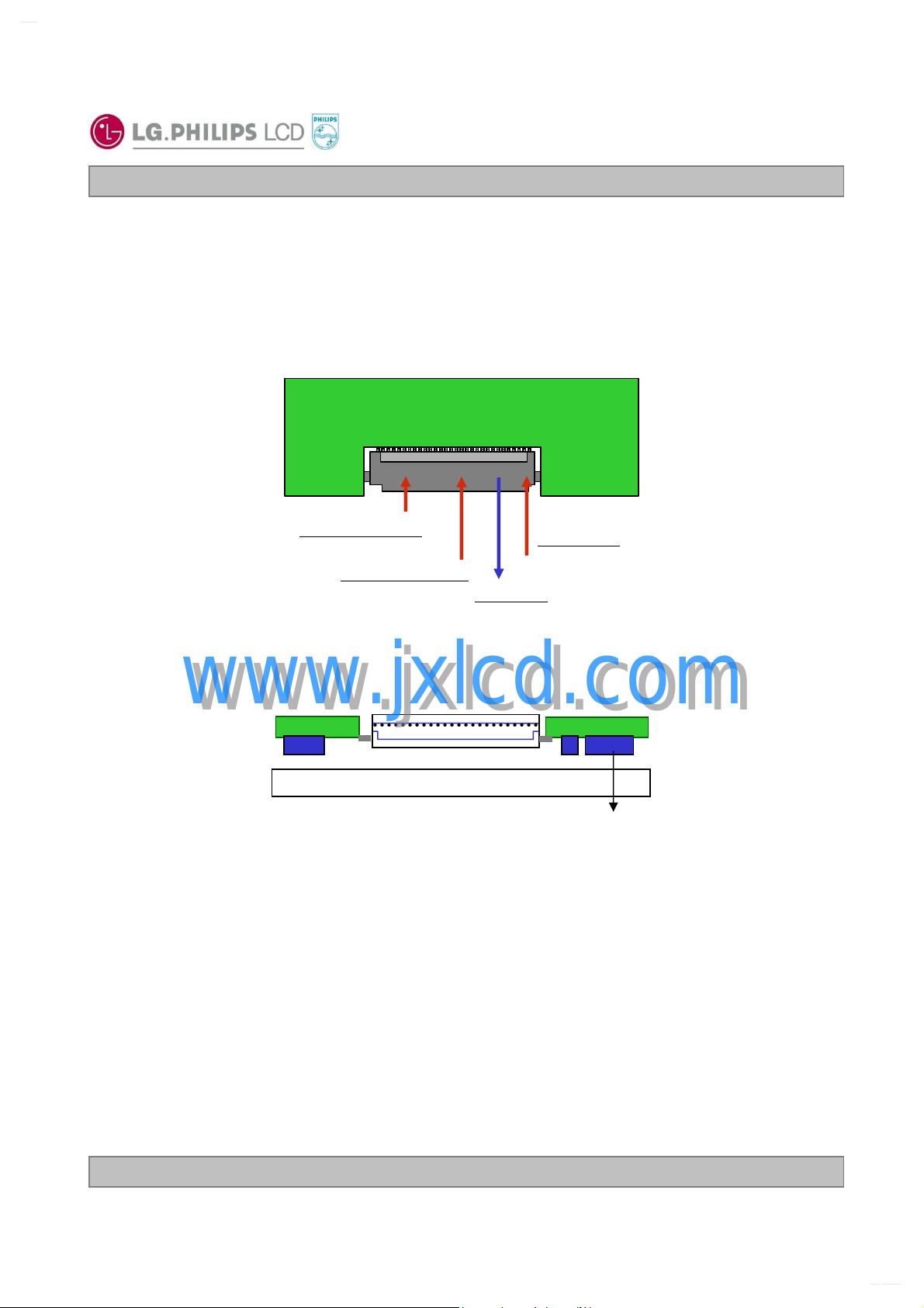
User Connector Diagram
MDF76LBRW-30S-1H(Hirose)
FI-XB30SRL-HF11 (JAE)
CN1
120
#30#1
LM220WE1
Liquid Crystal Display
1’st signal pairs
2’nd signal pairs
PWM_out
Input connector
www.jxlcd.com
www.jxlcd.com
Notes: 1. All GND(ground) pins should be connected together and should also be
connected to the LCD’s metal frame.
2. All V
(power input) pins should be connected together.
CC
#1 #30
Back Light
Rear view of LCM
Power(5V)
PCB
Components
3. All NC pins should be separated from other signal or power.
4. PWM_OUT signal controls the burst frequency of a inverter.
This signal is synchronized with vertical frequency,
it’s frequency is 3 times of vertical frequency, and it’s duty ratio is 50%.
If you don’t use this pin, it is no connection.
Ver. 0.1 Jun. 13. 2007
10 / 31
 Loading...