

SPECIFICATION
( ) Preliminary Specification
(◆) Final Specification
Title 21.5” Full HD TFT LCD
LM215WF4
Liquid Crystal Display
Product Specification
FOR
APPROVAL
BUYER
MODEL
www.jxlcd.com
www.jxlcd.com
SIGNATURE DATE
/
/
/
Asus
SUPPLIER LG Display Co., Ltd.
*MODEL LM215WF4
SUFFIX TLE7
*When you obtain standard approval,
please use the above model name without suffix
APPROVED BY
K.G. Park / G.Manager
REVIEWED BY
K.H. Oh / Manager [C]
H.D. Joo / Manager [M]
C.S. Shin / Manager [P]
PREPARED BY
S.H. Kim / Engineer
DATE
Please return 1 copy for your confirmation
With your signature and comments.
Ver. 1.0 Feb. 28. 2011
Product Engineering Dept.
LG Display Co., Ltd
1 / 32
Product Specification
Contents
LM215WF4
Liquid Crystal Display
No ITEM
COVER 1
CONTENTS 2
RECORD OF REVISIONS 3
1 GENERAL DESCRIPTION 4
2 ABSOLUTE MAXIMUM RATINGS 5
3 ELECTRICAL SPECIFICATIONS 6
1) ELECTRICAL CHARACTERISTICS 6
2) INTERFACE CONNECTIONS 8
3) LVDS characteristics 11
4) SIGNAL TIMING SPECIFICATIONS 14
5) SIGNAL TIMING WAVEFORMS 15
6) COLOR INPUT DATA REFERNECE 16
7) POWER SEQUENCE 17
8) POWER DIP CONDITION 18
4 OPTICAL SFECIFICATIONS 19
Page
5 MECHANICAL CHARACTERISTICS 25
6 RELIABILITY 28
7 INTERNATIONAL STANDARDS 29
8 PACKING 30
9 PRECAUTIONS 31
www.jxlcd.com
www.jxlcd.com
1) SAFETY 29
2) EMC 29
3) ENVIRONMENT 29
1) DESIGNATION OF LOT MARK 30
2) PACKING FORM 30
1) MOUNTING PRECAUTIONS 31
2) OPERATING PRECAUTIONS 31
3) ELECTROSTATIC DISCHARGE CONTROL 32
4) PRECAUTIONS FOR STRONG LIGHT EXPOSURE 32
5) STROAGE 32
6) HANDLING PRECAUTIONS FOR PROTECTION FILM 32
Ver. 1.0 Feb. 28. 2011
2 / 32
Product Specification
Record of revisions
LM215WF4
Liquid Crystal Display
Revision
No
Ver. 0.1 Dec. 10. 2010 - Preliminary Specifications
Ver. 0.2 Jan.21.2011 4
Ver. 1.0 Feb. 28. 2011 - Final Specifications
www.jxlcd.com
www.jxlcd.com
Date Page Description
integral Light Emitting Diode(LED) a Light Emitting
Diode (LED)
4 Update Fig.1 (W-LEDs)
7 Update LED string voltage (min -. min 46.4V)
10 Change 10019HR-06 to 10019HR-H06B
23 Change Notes 7 (Test pattern, Test point)
23 Update FIG.12
27 Update Rear View
30 Update 8-1. Note 1
Ver. 1.0 Feb. 28. 2011
3 / 32
LM215WF4
Liquid Crystal Display
Product Specification
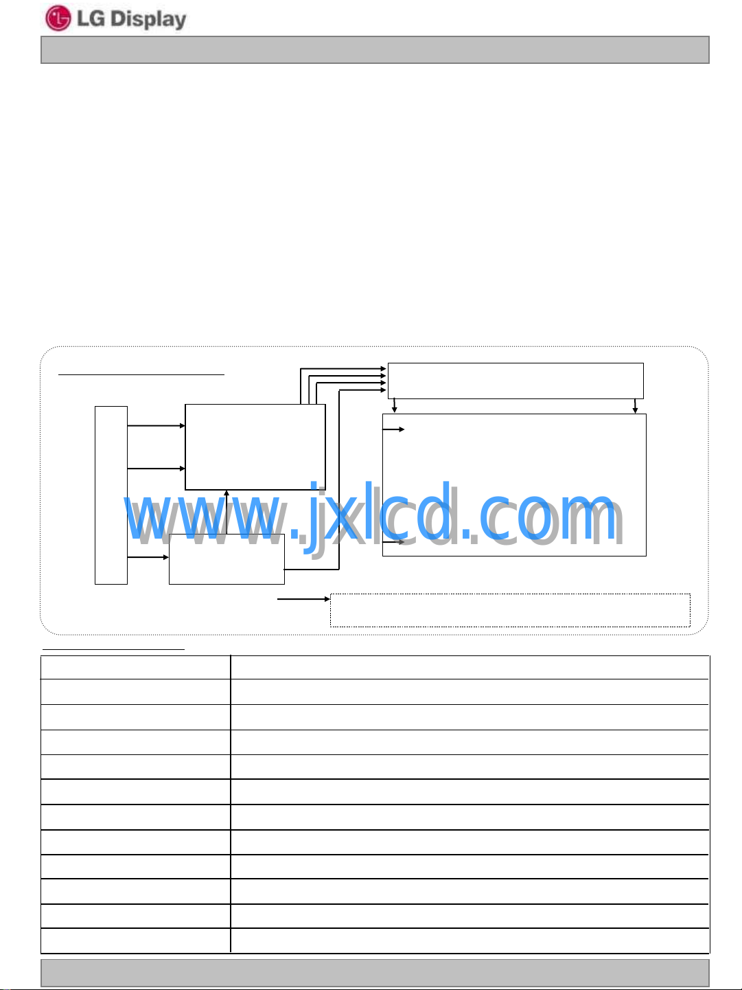
1. General description
LM215WF4-TLE7 is a Color Active Matrix Liquid Crystal Display with a Light Emitting Diode (LED)
backlight system. The matrix employs a-Si Thin Film Transistor as the active element. It is a
transmissive type display operating in the normally white mode. It has a 21.5 inch diagonally
measured active display area with Full HD resolution (1080 vertical by 1920 horizontal pixel array)
Each pixel is divided into Red, Green and Blue sub-pixels or dots which are arranged in vertical
stripes. Gray scale or the brightness of the sub-pixel color is determined with
a 8-bit gray scale signal for each dot, thus, presenting a palette of more than 16,7M colors with
Advanced-FRC(Frame Rate Control). It has been designed to apply the interface method that
enables low power, high speed, low EMI. FPD Link or compatible must be used as a LVDS(Low
Voltage Differential Signaling) chip. It is intended to support applications where thin thickness,
wide viewing angle, low power are critical factors and graphic displays are important. In
combination with the vertical arrangement of the sub-pixels, the LM215WF4-TLE7 characteristics
provide an excellent flat panel display for office automation products such as monitors.
FIG. 1 Block diagram
LVDS
pair #1
LVDS
pair #2
CN1
www.jxlcd.com
www.jxlcd.com
+5V
General features
Active screen size 21.53 inches (546.86mm) diagonal
Outline Dimension 495.6(H) x 292.2(V) x 10.2(D) mm(Typ.)
Pixel Pitch 0.08275*RGB(H)mm x 0.248(V)mm
Pixel Format 1920 horizontal By 1080 vertical Pixels. RGB stripe arrangement
Power circuit
VLCD
Timing
controller
block
VLED 2ch
RGB
Source driver circuit
S1
G1
TFT-LCD Panel
(1920×RGB×1080 pixels)
G1080
B/L System (W-LEDs)
S1920
Interface LVDS 2Port
Color depth 16.7M colors
Luminance, white 250 cd/m2 ( Center 1Point, typ)
Viewing Angle (CR>10) R/L 170(Typ.), U/D 160(Typ.)
Power Consumption
Weight 1,350g (Typ.)
Display operating mode Transmissive mode, normally White
Surface treatments
Ver. 1.0 Feb. 28. 2011
Total 16.21 W(Typ.), (4.95 W@V
Hard coating (3H), Anti-glare treatment of the front polarizer
LCD
, 11.26 W@ILED = 110mA)
4 / 32
Product Specification
2. Absolute maximum ratings
The following are maximum values which, if exceeded,
may cause faulty operation or damage to the unit.
Table 1. Absolute maximum ratings
LM215WF4
Liquid Crystal Display
Parameter Symbol
Power Supply Input Voltage V
Operating Temperature T
Storage Temperature T
Operating Ambient Humidity H
Storage Humidity H
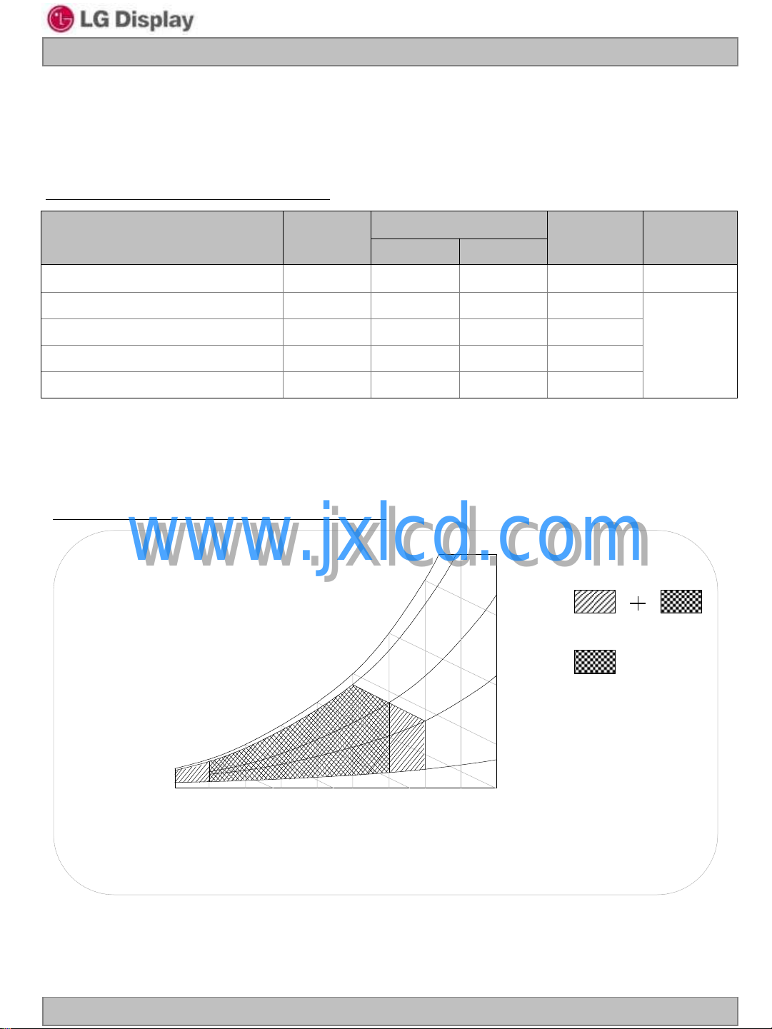
Note : 1. Temperature and relative humidity range are shown in the figure below.
Wet bulb temperature should be 39 °C Max, and no condensation of water.
Note : 2. Storage condition is guaranteed under packing condition.
FIG. 2 Temperature and relative humidity
www.jxlcd.com
www.jxlcd.com
Wet Bulb
Temperature [℃]
20
10
0
LCD
OP
ST
OP
ST
50
40
30
Values
Min Max
-0.3 +6.0 Vdc
0 50
-20 60
10 90 %RH
10 90 %RH
90%
60
60%
40%
10%
Units Notes
°C
°C
Humidity
[(%)RH]
Storage
Operation
At 25℃
1, 2
10 20 30 40 50 60 70 800-20
Dry Bulb Temperature [℃]
Ver. 1.0 Feb. 28. 2011
5 / 32
LM215WF4
Liquid Crystal Display
Product Specification
3. Electrical specifications
3-1. Electrical characteristics
It requires two power inputs. One is employed to power the LCD electronics and to drive the
TFT array and liquid crystal. The second input power for the LED Backlight, is typically
generated by an LED Driver. The LED driver is an external unit to the LCDs.
Table 2. Electrical characteristics
Parameter Symbol
MODULE :
Power Supply Input Voltage V
Permissive Power Input Ripple V
Power Supply Input Current
Power Consumption P
Inrush current I
Note :
1. The specified current and power consumption are
under the VLCD=5.0V, 25 2°C,fV=60Hz condition
whereas mosaic pattern(8 x 6) is displayed and fVis the frame frequency.
2. The current is specified at the maximum current pattern and L80.
3. Permissive power ripple should be measured under VCC=5.0V, 25°C, fV (frame frequency)=75Hz
condition and At that time, we recommend the bandwidth configuration of oscilloscope
is to be under 20MHz.
4. The duration of rush current is about 5ms and rising time of power Input is 500us 20%.
www.jxlcd.com
www.jxlcd.com
LCD
LCD
I
LCD-MOSAIC
I
LCD-BLACK
I
LCD-L80
LCD
RUSH
Min Typ Max
4.5 5.0 5.5 Vdc
- - 400 mV
- 990 1290 mA 1
- 1320 1715 mA 2
- 930 1210 mA 2
- 4.95 6.45 Watt 1
- - 3.5 A 4
Values
Unit Notes
p-p
3
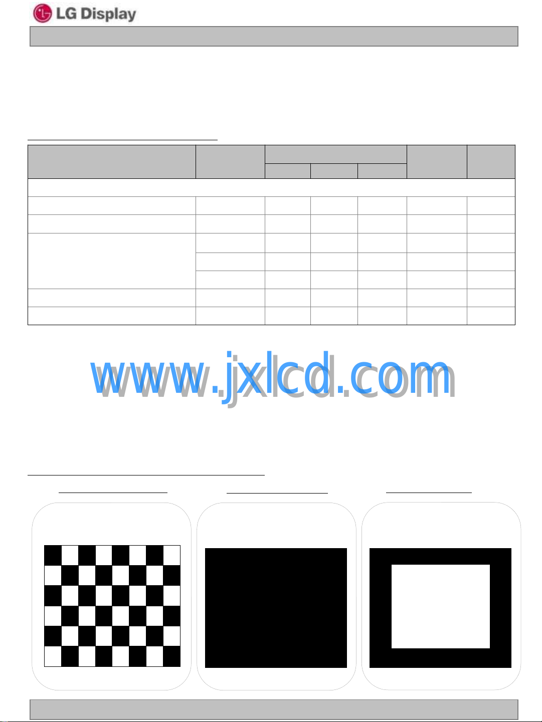
FIG.3 pattern for Electrical characteristics
power consumption
White : 255Gray
Black : 0Gray
Mosaic Pattern(8 x 6)
Ver. 1.0 Feb. 28. 2011
power input ripple
Full Black Pattern
Energy star 5.0
White : 255Gray (64%)
Black : 0Gray (36%)
L80 Pattern
6 / 32
Product Specification
Table 3. LED array ELECTRICAL CHARACTERISTICS
LM215WF4
Liquid Crystal Display
Parameter Symbol Condition
LED : 1
LED String Current Is - 110 120 mA 2
LED String Voltage Vs 46.4 51.2 56 V 3
Power
Consumption
LED Life Time LED_LT 30,000 - - Hrs 5
LED driver design guide
: The design of the LED driver must have specifications for the LED in LCD Assembly.
The performance of the LED in LCM, for example life time or brightness, is extremely
influenced by the characteristics of the LED driver.
So all the parameters of an LED driver should be carefully designed and output current
should be Constant current control.
Please control feedback current of each string individually to compensate
www.jxlcd.com
the current variation among the strings of LEDs.
www.jxlcd.com
When you design or order the LED driver, please make sure unwanted lighting caused by
the mismatch of the LED and the LED driver (no lighting, flicker, etc) never occurs.
When you confirm it, the LCD module should be operated in the same condition
as installed in your instrument.
Parray - 11.26 12.32 Watt 4,6
Min. Typ. Max.
Values
Unit Notes
Notes :
1. Specified values are for a single LED bar.
2. The specified current is input LED chip 100% duty current.
3. The specified voltage is input LED string voltage at typical 110mA 100% duty current.
4. The specified power consumption is input LED bar power consumption
at typical 110mA 100% duty current.
5. The life time is determined as the time at which luminance of the LED is 50%
compared to that of initial value at the typical LED current on condition of continuous
operating at 25 2°C.
6. The LED bar power consumption shown above does not include loss of external driver.
The used LED string current is the LED typical current.
Typ Power Consumption is calculated with PBar = Vs(Typ.) x Is(Typ.) x Nstring
Max Power Consumption is calculated with PBar = Vs(Max.) x Is(Typ) x Nstring
Ver. 1.0 Feb. 28. 2011
7 / 32
Liquid Crystal Display
Product Specification
3-2. Interface connections
3-2-1. LCD Module
LCD connector(CN1) : GT103-30S-HF15-E2500 (LSM) , IS100-L30O-C23(UJU)
Mating connector : FI-X30H and FI-X30HL (JAE) or Equivalent
Table 4. Module connector(CN1) pin configuration
LM215WF4
Pin No
1
2
3
4
5
6
7
8
9
10
11
12
13
14
15
16
17
18
19
20
21
22
23
24
25
26
27
28
29
30
Symbol Description
RXO0-
RXO0+
RXO1-
RXO1+
RXO2-
RXO2+
GND
RXOC-
RXOC+
RXO3-
RXO3+
RXE0-
www.jxlcd.com
www.jxlcd.com
RXE0+
GND
RXE1-
RXE1+
GND
RXE2-
RXE2+
RXEC-
RXEC+
RXE3-
RXE3+
GND
NC
NC
PWM_OUT
VLCD
VLCD
VLCD
Minus signal of 1st channel 0 (LVDS)
Plus signal of 1st channel 0 (LVDS)
Minus signal of 1st channel 1 (LVDS)
Plus signal of 1st channel 1 (LVDS)
Minus signal of 1st channel 2 (LVDS)
Plus signal of 1st channel 2 (LVDS)
Ground (AGP)
Minus signal of 1st clock channel (LVDS)
Plus signal of 1st clock channel (LVDS)
Minus signal of 1st channel 3 (LVDS)
Plus signal of 1st channel 3 (LVDS)
Minus signal of 2nd channel 0 (LVDS)
Plus signal of 2nd channel 0 (LVDS)
Ground
Minus signal of 2nd channel 1 (LVDS)
Plus signal of 2nd channel 1 (LVDS)
Ground
Minus signal of 2nd channel 2 (LVDS)
Plus signal of 2nd channel 2 (LVDS)
Minus signal of 2nd clock channel (LVDS)
Plus signal of 2nd clock channel (LVDS)
Minus signal of 2nd channel 3 (LVDS)
Plus signal of 2nd channel 3 (LVDS)
Ground
No Connection (For LCD internal use only.)
No Connection (For LCD internal use only.)
Reference signal for LED Driver control
Power Supply (5.0V)
Power Supply (5.0V)
Power Supply (5.0V)
Ver. 1.0 Feb. 28. 2011
8 / 32
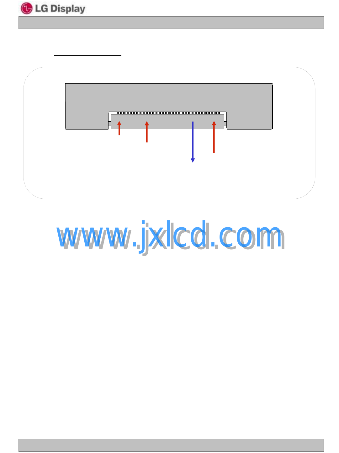
FIG. 4 Connector diagram
#1 #30
1‟st signal pairs
Product Specification
GT103-30S-HF15-E2500 (LSM)
#
1
2‟nd signal pairs
Power(+5V)
PWM_OUT
Rear view of LCM
LM215WF4
Liquid Crystal Display
#30
Note:
1. NC: No Connection.
2. All GND(ground) pins should be connected together and to Vss which should also
be connected to the LCD‟s metal frame.
www.jxlcd.com
www.jxlcd.com
3. All V
4. Input Level of LVDS signal is based on the IEA 664 Standard.
5. PWM_OUT is a reference signal for LED Driver control.
This PWM signal is synchronized with vertical frequency.
Its frequency is 6 times of vertical frequency, and its duty ratio is 50%.
If the system don‟t use this pin, do not connect.
(power input) pins should be connected together.
LCD
Ver. 1.0 Feb. 28. 2011
9 / 32
LM215WF4
Liquid Crystal Display
Product Specification
3-2-2. LED Interface
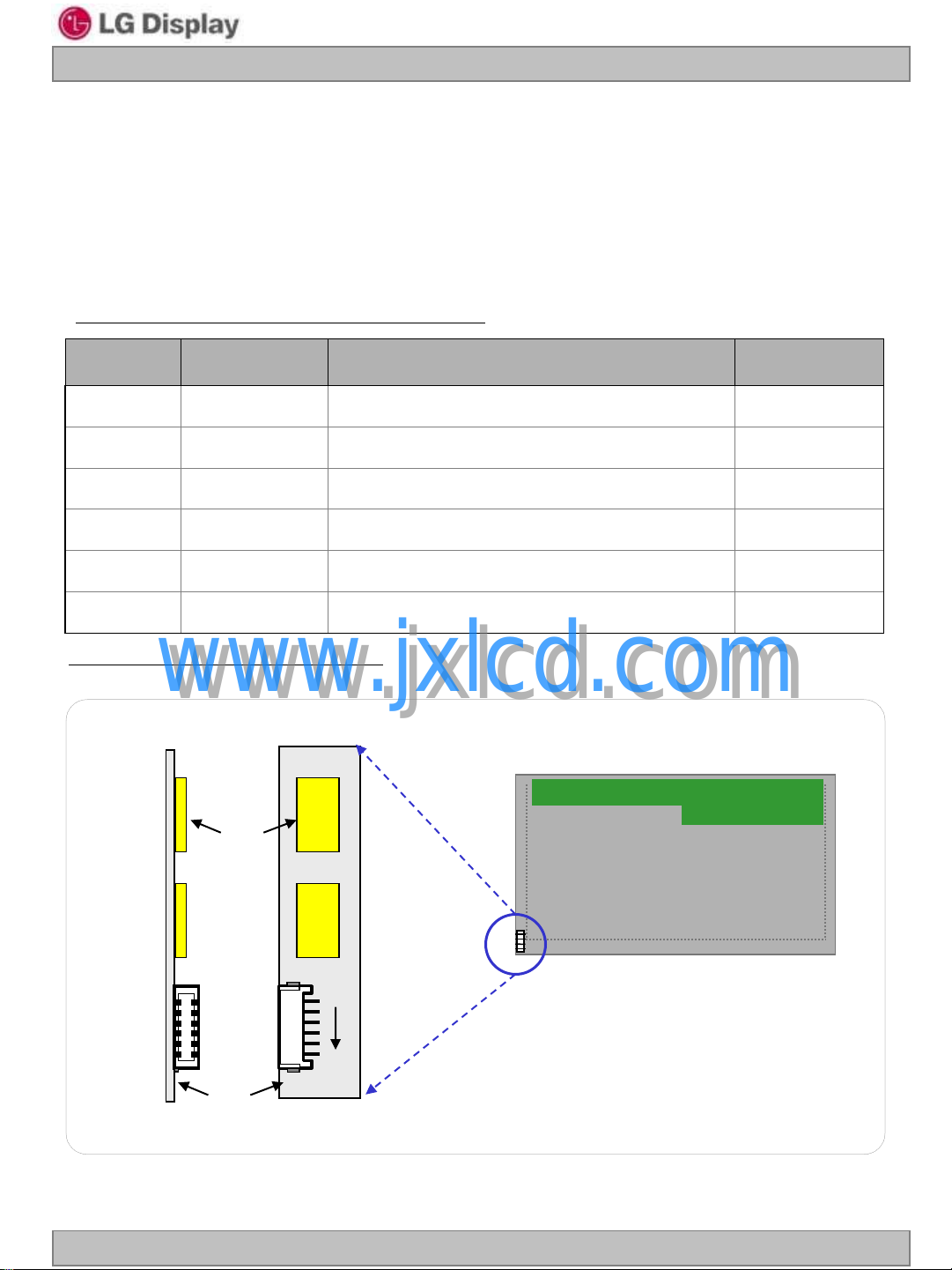
The LED interface connector is a model 10019HR-H06B manufactured by Yeonho Electronics.
The mating connector should be used a FFC/FPC specified in LED interface connector specification.
The pin configuration for the connector is shown in the table below.
Table 5. LED connector pin configuration
Pin Symbol Description Notes
1 FB1 Channel1 Current Feedback
2 NC No connection
3 VLED LED Power Supply
4 VLED LED Power Supply
5 NC No connection
6 FB2 Channel2 Current Feedback
FIG. 5 Backlight connector view
www.jxlcd.com
www.jxlcd.com
LED
1
Back View
6
PCB
Ver. 1.0 Feb. 28. 2011
10 / 32
 Loading...