

Product Specification
SPECIFICATION
LM215WF4
Liquid Crystal Display
( ● ) Preliminary Specification
( ) Final Specification
BUYER
MODEL
www.jxlcd.com
www.jxlcd.com
APPROVED BY
/
APPROVAL
General
SIGNATURE
DATE
FOR
215” Full HD TFT LCDTitle
LG. Display Co., Ltd.SUPPLIER
LM215WF4*MODEL
TLA1SUFFIX
*When you obtain standard approval,
please use the above model name without suffix
APPROVED BY
S.Y. PARK / G.Manager
SIGNATURE
DATE
/
/
Please return 1 copy for your confirmation with
your signature and comments.
Ver. 0.0 Nov. 19. 2009
REVIEWED BY
K. H. CHOI / Manager [C]
D. Y. KIM / Manager [M]
D. Y. SEOK / Manager [P]
PREPARED BY
S. Y. KIM / Engineer
MNT Product Engineering Dept.
LG Display Co., Ltd
1 / 31
Product Specification
Contents
LM215WF4
Liquid Crystal Display
PageITEMNo
COVER
CONTENTS
RECORD OF REVISIONS
GENERAL DESCRIPTION1
ABSOLUTE MAXIMUM RATINGS2
ELECTRICAL SPECIFICATIONS3
ELECTRICAL CHARACTREISTICS 3-1
INTERFACE CONNECTIONS 3-2
SIGNAL TIMING SPECIFICATIONS 3-3
SIGNAL TIMING WAVEFORMS 3-4
COLOR DATA REFERNECE 3-5
POWER SEQUENCE 3-6
www.jxlcd.com
www.jxlcd.com
V
POWER DIP CONDITION 3-7
LCD
OPTICAL SFECIFICATIONS4
MECHANICAL CHARACTERISTICS5
1
2
3
4
5
6
6
9
15
16
17
18
19
20
24
RELIABLITY6
INTERNATIONAL STANDARDS7
SAFETY 7-1
EMC 7-2
PACKING8
DESIGNATION OF LOT MARK 8-1
PACKING FORM 8-2
PRECAUTIONS9
Ver. 0.0 Nov. 19. 2009
27
28
28
28
29
29
29
30
2 / 31
Product Specification
RECORD OF REVISIONS
First Draft(Preliminary)-Nov. 19. 20090.0
LM215WF4
Liquid Crystal Display
DescriptionPageRevision DateRevision No
www.jxlcd.com
www.jxlcd.com
Ver. 0.0 Nov. 19. 2009
3 / 31
LM215WF4
Liquid Crystal Display
Product Specification
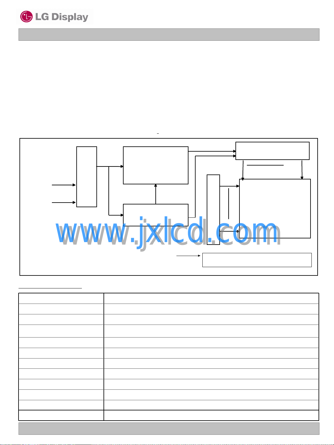
1. General Description
LM215WF4 is a Color Active Matrix Liquid Crystal Display with a Light Emitting Diode ( White LED) backlight
system without LED driver. The matrix employs a-Si Thin Film Transistor as the active element.
It is a transmissive type display operating in the normally White mode. It has a 215 inch diagonally measured
active display area with FHD resolution (1080 vertical by 1920horizontal pixel array)
Each pixel is divided into Red, Green and Blue sub-pixels or dots which are arranged in vertical stripes.
Gray scale or the brightness of the sub-pixel color is determined with a 8-bit gray scale signal for each dot,
thus, presenting a palette of more than 16,7M colors with A-FRC(Advanced Frame Rate Control).
It has been designed to apply the 8Bit 2 port LVDS interface.
It is intended to support displays where high brightness, super wide viewing angle,
high color saturation, and high color are important.
RGB, Dclk, DE
Hsync, Vsync
(LVDS 2 port)
V
(+5V)
LCD
www.jxlcd.com
www.jxlcd.com
General Features
CN1
(30pin)
Source Driver Circuit
Timing Control
Block
G1
Gate Driver circuit
TFT-LCD Panel
Power Circuit Block
G1080
Vled 2ch
Figure 1. Block diagram
21.53 inches(546.86mm) diagonalActive Screen Size
495.6(H) x 292.2(V) x 11.5(D) mm (Typ.)Outline Dimension
0.248 mm x 0.248mmPixel Pitch
B/L System (White LED)
(1920 1080 pixels)
S1920S1
1920 horiz. By 1080 vert. Pixels RGB stripes arrangementPixel Format
16.7M colors (6bit + A FRC)Color Depth
250 cd/m
View Angle Free (R/L 170(Typ.), U/D 160(Typ.))Viewing Angle(CR>10)
Total 16.2 (Typ.), (3.5@V
1550 (Typ.), 1630g(Max.)Weight
Transmissive mode, normally whiteDisplay Operating Mode
Hard coating(3H), Anti-glare treatment of the front polarizerSurface Treatment
Color Gamut
Ver. 0.0 Nov. 19. 2009
68% CIE1931
2
( Center 1 points)Luminance, White
LCD
, 12.7@IBL =110mA)Power Consumption
4 / 31
LM215WF4
Liquid Crystal Display
Product Specification
2. Absolute Maximum Ratings
The following are maximum values which, if exceeded, may cause faulty operation or damage to the unit.
Table 1. ABSOLUTE MAXIMUM RATINGS
Parameter Notes
Power Input Voltage
Operating Temperature
Storage Temperature
Operating Ambient Humidity
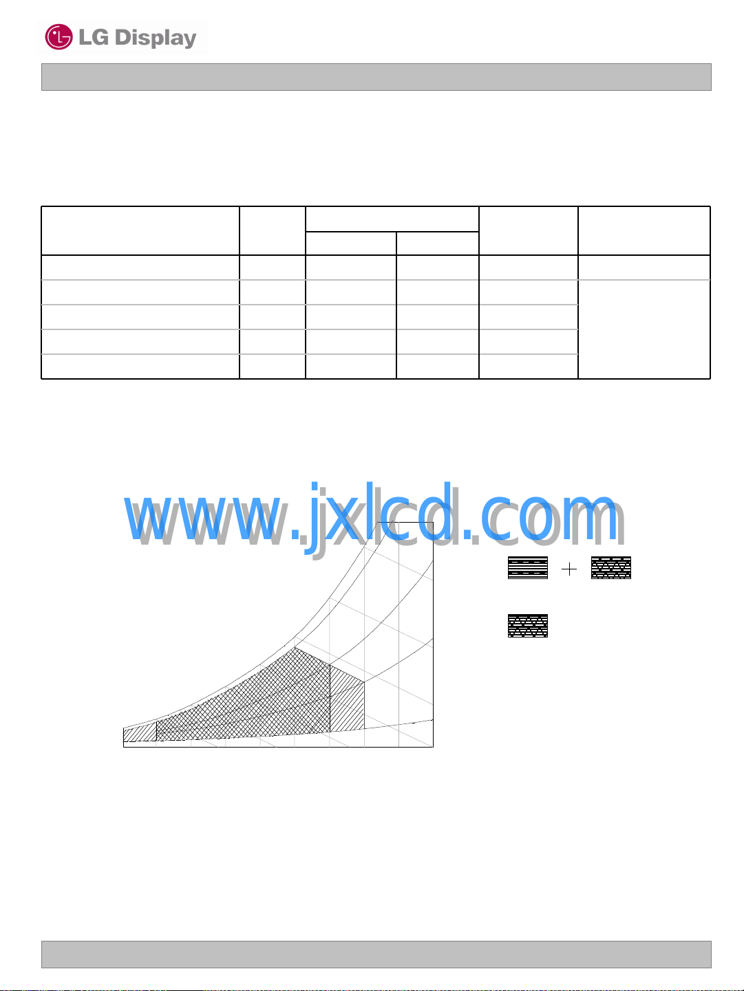
Storage Humidity
Note : 1. Temperature and relative humidity range are shown in the figure below.
Wet bulb temperature should be 39 °C Max, and no condensation of water.
Note : 2. Storage condition is guaranteed under packing condition.
www.jxlcd.com
www.jxlcd.com
Wet Bulb
Temperature [C]
10
0
Symbol
50
40
30
20
Values
MaxMin
500TOP
60-20TST
90%
60
60%
Hu
mi
di
ty
40%
[(
%)
RH
]
10%
Units
Vdc5.54.5VLCD
°C
°C
%RH9010HOP
%RH9010HST
Storage
Operation
at 25 2°C
1, 2
10 20 30 40 50 60 70 800-20
Dry Bulb Temperature [C]
Figure 2. Temperature and relative humidity
Ver. 0.0 Nov. 19. 2009
5 / 31
LM215WF4
Liquid Crystal Display
Product Specification
3. Electrical Specifications
3-1. Electrical Characteristics
It requires two power inputs. One is employed to power the LCD electronics and to drive the TFT array and
liquid crystal. The second input power for the LED/Backlight, is typically generated by an LED driver. The
driver is an external unit to the LCDs.
Table 2-1. ELECTRICAL CHARACTERISTICS
Parameter Symbol
MODULE :
VLCD Power Supply Input Voltage
Differential Impedance
ILCD Power Supply Input Current
Power Consumption
www.jxlcd.com
www.jxlcd.com
Note :
1. Permissive power ripple should be measured under VCC=5.0V, 25°C, fV(frame frequency)=MAX
condition and At that time, we recommend the bandwidth configuration of oscilloscope is to be under
20Mhz. See the next page.
2. The specified current and power consumption are under the V
whereas Mosaic and max power pattern shown in the [ Figure 3 ] is displayed.
-
-
-Pc TYP
-Pc MAX
Values
3.5
4.5
=5.0V, 25 2°C,f
LCD
MaxTypMin
5.554.5
805700
1035900
Vdc
Ohm11010090Zm
=60Hz condition
V
NotesUnit
1mVp-p400VdRF Permissive Power Input Ripple
2mA
3mA
2Watt
3Watt
4A3.0--IRUSH Rush current
3. The current is specified at the maximum current pattern.
4. Maximum Condition of Inrush current :
The duration of rush current is about 2ms and rising time of Input Voltage is 1ms(min.).
At any rising time of Input voltage, Keep the I2T Value by below Condition
Condition : I2T < 32*2ms
Ver. 0.0 Nov. 19. 2009
6 / 31
LM215WF4
Liquid Crystal Display
Product Specification
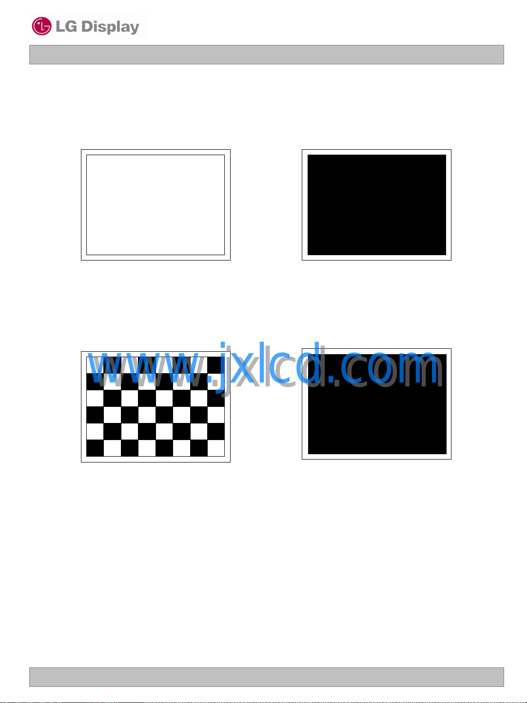
Permissive Power input ripple (VCC=5.0V, 25°C, fV(frame frequency)=MAX condition)•
White pattern
Power consumption (VCC=5.0V, 25°C, fV (frame frequency=60Hz condition)•
www.jxlcd.com
www.jxlcd.com
Typical power Pattern
Figure 3. Mosaic pattern & Black Pattern for power consumption measurement
Black pattern
Max power Pattern
Ver. 0.0 Nov. 19. 2009
7 / 31
Product Specification
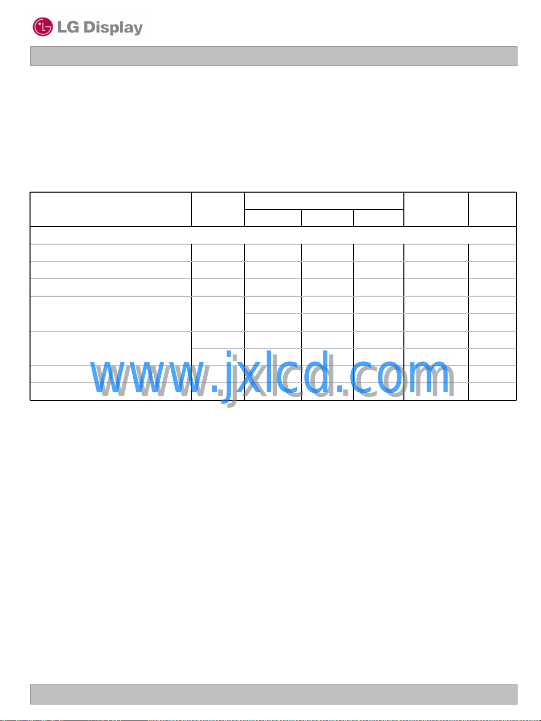
Table 2_2. LED Bar ELECTRICAL CHARACTERISTICS
LM215WF4
Liquid Crystal Display
ConditionSymbolParameter
Power Consumption
LED driver design guide
: The design of the LED driver must have specifications for the LED in LCD Assembly.
The performance of the LED in LCM, for example life time or brightness, is extremely
influenced by
the characteristics of the LED driver.
So all the parameters of an LED driver should be carefully designed and output current should be
Constant current control.
When you design or order the LED driver, please make sure unwanted lighting caused by
the mismatch of the LED and the LED driver (no lighting, flicker, etc) never occurs.
When you confirm it, the LCD module should be operated in the same condition as installed in
your instrument.
www.jxlcd.com
www.jxlcd.com
Values
Max.Typ.Min.
Unit
Notes
1,7LED :
2,7mA160110-IsLED String Current
3,7V61.257.654.0VsLED String Voltage
4,6,7Watt13.512.711.9PBar
5,7Hrs--30,000LED_LTLED Life Time
7℃70--TjLED Junction Temperature
1. Specified values are for a single LED bar.
2. The specified current is input LED chip 100% duty current.
3. The specified voltage is input LED string and Bar voltage at typical 110 mA 100% duty current.
4. The specified power consumption is input LED bar power consumption at typical 110 mA 100% duty current.
5. The life is determined as the time at which luminance of the LED is 50% compared to that of initial
value at the typical LED current on condition of continuous operating at 25 2°C.
6. The LED bar power consumption shown above does not include loss of external driver.
The used LED bar current is the LED typical current.
Min Power Consumption is calculated with PBar = Vs(Min.) x Is(Typ.) x Nstring
Max Power Consumption is calculated with PBar = Vbar(Max.) x Is(Typ) x Nstring
7. LED operating DC Forward Current and Junction Temperature must not exceed LED Max Ratings at 25 2°C.
Ver. 0.0 Nov. 19. 2009
8 / 31
LM215WF4
Liquid Crystal Display
Product Specification
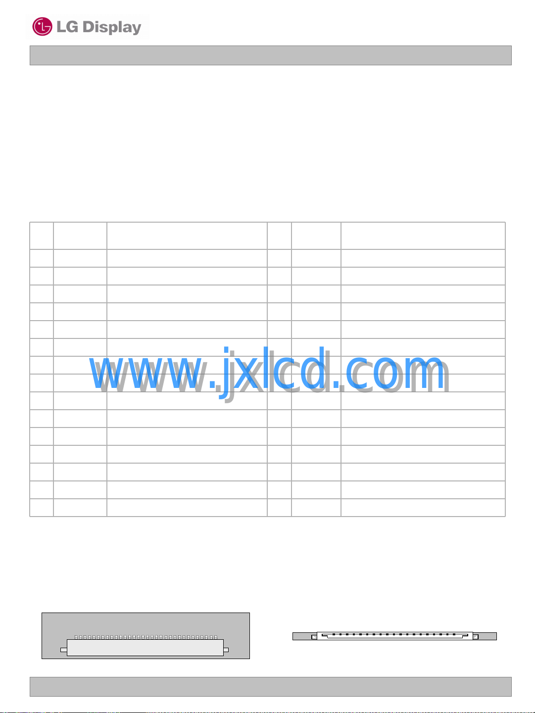
3-2. Interface Connections
This LCD employs Two interface connections, a 30 pin connector is used for the module electronics and a
4Pin Connector is used for the integral backlight system.
3-2-1. LCD Module
LCD Connector(CN1): GT103-30S-HF15-E2500, (Manufactured by LSC ) -
Mating Connector : FI-X30C2L (Manufactured by JAE) or Equivalent-
Table 3 MODULE CONNECTOR(CN1) PIN CONFIGURATION
Symbol
SymbolNo
Description
No
Symbol
1
2
3
4
5
6
7
8
9
10
11
12
13
14
15
FR0M
FR0P
FR1M
FR1P
FR2M
FR2P
GND
FCLKINM
www.jxlcd.com
FCLKINP
FR3M
FR3P
SR0M
SR0P
GND
SR1M
Minus signal of odd channel 0 (LVDS)
Plus signal of odd channel 0 (LVDS)
Minus signal of odd channel 1 (LVDS)
Plus signal of odd channel 1 (LVDS)
Minus signal of odd channel 2 (LVDS)
Plus signal of odd channel 2 (LVDS)
Ground
Minus signal of odd clock channel (LVDS)
www.jxlcd.com
Plus signal of odd clock channel (LVDS)
Minus signal of odd channel 3 (LVDS)
Plus signal of odd channel 3 (LVDS)
Minus signal of even channel 0 (LVDS)
Plus signal of even channel 0 (LVDS)
Ground
Minus signal of even channel 1 (LVDS)
16
17
18
19
20
21
22
23
24
25
26
27
28
29
30
SR1P
GND
SR2M
SR2P
SCLKINM
SCLKINP
SR3M
SR3P
GND
NC
NC
PWM_OUT
VLCD
VLCD
VLCD
Plus signal of even channel 1 (LVDS)
Ground
Minus signal of even channel 2 (LVDS)
Plus signal of even channel 2 (LVDS)
Minus signal of even clock channel (LVDS)
Plus signal of even clock channel (LVDS)
Minus signal of even channel 3 (LVDS)
Plus signal of even channel 3 (LVDS)
Ground
No Connection
No Connection
For Control Burst frequency of Inverter
Power Supply +5.0V
Power Supply +5.0V
Power Supply +5.0V
Note: 1. All GND(ground) pins should be connected together and to Vss which should also be connected to
the LCD’s metal frame.
2. All VLCD (power input) pins should be connected together.
3. Input Level of LVDS signal is based on the IEA 664 Standard.
Rear view of LCM
#1 #30
GT103-30S-HF15-E2500(LSC )
Ver. 0.0 Nov. 19. 2009
#1 #30
[ Figure 4 ] Connector diagram
9 / 31
Liquid Crystal Display
Product Specification
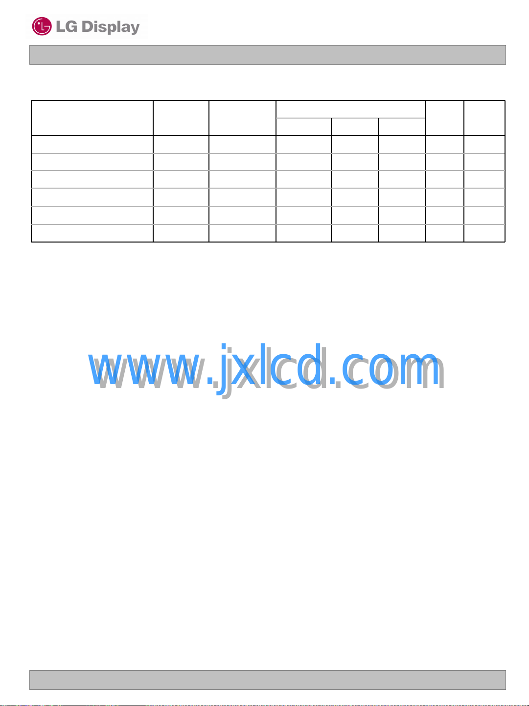
Table 4. REQUIRED SIGNAL ASSIGNMENT FOR Flat Link (TI:SN75LVDS83) Transmitter
Pin # Require SignalPin Name Pin # Require SignalPin Name
1 Power Supply for TTL InputVCC 29 Ground pin for TTLGND
2 TTL Input (R7)D5 30 TTL Input (DE)D26
3 TTL Input (R5)D6 31 TTL Level clock InputTX CLKIN
4 TTL Input (G0)D7 32 Power Down InputPWR DWN
5 Ground pin for TTLGND 33 Ground pin for PLLPLL GND
6 TTL Input (G1)D8 34 Power Supply for PLLPLL VCC
7 TTL Input (G2)D9 35 Ground pin for PLLPLL GND
8 TTL Input (G6)D10 36 Ground pin for LVDSLVDS GND
9 Power Supply for TTL InputVCC 37 Positive LVDS differential data output 3TxOUT3+
10 TTL Input (G7)D11 38 Negative LVDS differential data output 3TxOUT3-
LM215WF4
11 TTL Input (G3)D12 39 Positive LVDS differential clock outputTX CLKOUT+
12 TTL Input (G4)D13 40 Negative LVDS differential clock outputTX CLKOUT-
13 Ground pin for TTLGND 41 Positive LVDS differential data output 2TX OUT2+
14 TTL Input (G5)D14 42 Negative LVDS differential data output 2TX OUT2-
15 TTL Input (B0)D15 43 Ground pin for LVDSLVDS GND
16 TTL Input (B6)D16 44 Power Supply for LVDSLVDS VCC
17 Power Supply for TTL InputVCC 45 Positive LVDS differential data output 1TX OUT1+
19 TTL Input (B1)D18
20 TTL Input (B2)D19
22 TTL Input (B3)D20
23 TTL Input (B4)D21
24 TTL Input (B5)D22
25 TTL Input (RSVD)D23
26 Power Supply for TTL InputVCC 54 TTL Input (R2)D2
www.jxlcd.com
www.jxlcd.com
46 Negative LVDS differential data output 1TX OUT1-18 TTL Input (B7)D17
47 Positive LVDS differential data output 0TX OUT0+
48 Negative LVDS differential data output 0TX OUT0-
49 Ground pin for LVDSLVDS GND21 Ground pin for TTL InputGND
50 TTL Input (R6)D27
51 TTL Input (R0)D0
52 TTL Input (R1)D1
53 Ground pin for TTLGND
55 TTL Input (R3)D327 TTL Input (HSYNC)D24
56 TTL Input (R4)D428 TTL Input (VSYNC)D25
Notes : Refer to LVDS Transmitter Data Sheet for detail descriptions.
Ver. 0.0 Nov. 19. 2009
10 / 31
 Loading...