

LG LM-215WF3-SDC2 Service manual
( ) Preliminary Specification
( ● ) Final Specification
LM215WF3
Liquid Crystal Display
Product Specification
SPECIFICATION
FOR
APPROVAL
21.5” Full HD TFT LCDTitle
BUYER
www.jxlcd.com
www.jxlcd.com
APPROVED BY
/
/
/
APPLE
K60MODEL
SIGNATURE
DATE
SUPPLIER LG Display Co., Ltd.
*MODEL LM215WF3
SUFFIX SDC2
*When you obtain standard approval,
please use the above model name without suffix
APPROVED BY
S. Y. Park / G.Manager
REVIEWED BY
D. Y. KIM / Manager [C]
D. Y. KIM/ Manager [M]
S. H. Cho / Manager [P]
PREPARED BY
Y. T. YOO / Engineer
SIGNATURE
DATE
Please return 1 copy for your confirmation with
your signature and comments.
Ver. 1.0 January. 13 . 2011
MNT Products Engineering Dept.
LG Display Co., Ltd
1 / 35
LM215WF3
Liquid Crystal Display
Product Specification
Contents
No ITEM Page
COVER
CONTENTS
RECORD OF REVISIONS
1 GENERAL DESCRIPTION
2 ABSOLUTE MAXIMUM RATINGS
3 ELECTRICAL SPECIFICATIONS
3-1 ELECTRICAL CHARACTREISTICS
3-2 INTERFACE CONNECTIONS
3-3 SIGNAL TIMING SPECIFICATIONS
3-4 SIGNAL TIMING WAVEFORMS
3-5 COLOR INPUT DATA REFERNECE
3-6 POWER SEQUENCE
4 OPTICAL SFECIFICATIONS
5 MECHANICAL CHARACTERISTICS
6 RELIABLITY
www.jxlcd.com
www.jxlcd.com
1
2
4
5
6
7
7
9
12
13
14
15
18
24
27
7 INTERNATIONAL STANDARDS
7-1 SAFETY
7-2 EMC
7-3 ENVIRONMENT
8 PACKING
8-1 DESIGNATION OF LOT MARK
8-2 PACKING FORM
9 PRECAUTIONS 30
9-1 MOUNTING PRECAUTIONS 30
9-2 OPERATING PRECAUTIONS 30
9-3 ELECTROSTATIC DISCHARGE CONTROL 31
9-4 PRECAUTIONS FOR STRONG LIGHT EXPOSURE 31
9-5 STORAGE 31
9-6 HANDLING PRECAUTIONS FOR PROTECTION FILM 31
Ver. 1.0 January. 13 . 2011
28
28
28
28
29
29
29
2 / 35
LM215WF3
Liquid Crystal Display
Product Specification
Contents
No ITEM Page
10 EDID DATA 32
10-1 EDID DATA 32
10-2 EDID READ/WRITE PROTOCOL 35
www.jxlcd.com
www.jxlcd.com
Ver. 1.0 January. 13 . 2011
3 / 35
Product Specification
RECORD OF REVISIONS
LM215WF3
Liquid Crystal Display
Revision
No
0.0 Sep.15 . 2010 - First Draft (Preliminary)
1.0 Jan.13 . 2011 32~35 Update EDID
Revision Date Page Description
www.jxlcd.com
www.jxlcd.com
Ver. 1.0 January. 13 . 2011
4 / 35
LM215WF3
Liquid Crystal Display
Product Specification
1. General Description
LM215WF3 is a Color Active Matrix Liquid Crystal Display with Light Emitting Diode ( White LED) backlight
system without LED driver. The matrix employs a-Si Thin Film Transistor as the active element.
It is a transmissive type display operating in the normally black mode. It has a 21.5inch diagonally
measured active display area with Full HD resolution (1920 vertical by 1080 horizontal pixel array)
Each pixel is divided into Red, Green and Blue sub-pixels or dots which are arranged in vertical stripes.
Gray scale or the brightness of the sub-pixel color is determined with a 8bit gray scale signal for each dot,
th u s, pr ese nt in g a p a le tt e of mo r e t ha n 16M co lor s. .
It has been designed to apply the 8bit 4Lane Display port interface.
It is in te nd ed to s up po rt di spl ay s wh er e h i g h b ri gh t n e s s , s u pe r w id e vi ew in g a ng le,
high color saturation, and high color are important.
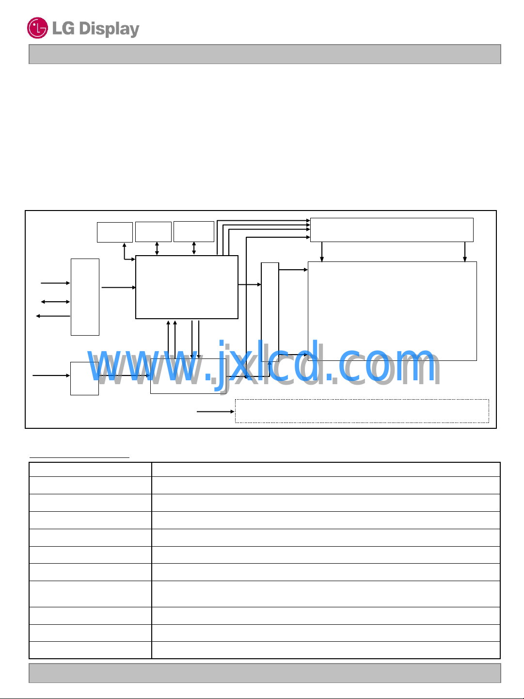
RGB
Flash
Memory
SPI
Logic Power
3.3V / 1.2V
EEPROM
I2C
Timing
Controller
Power
Enable
(Video On)
Source Driver Circuit
S1 S1920
G1
Gate Driver Circuit
TFT - LCD Panel
(1920 × RGB × 1080 pixels)
G1080
Main Link
4 Lane
AUX CH
HPD
EEPROM
(LUT)
I2C
CN1
(30pin)
LCD Power
12 V
CN2
www.jxlcd.com
www.jxlcd.com
(6pin)
Power Circuit
Block
VLED 2ch
[ Figure 1 ] Block diagram
B/L System (White LED)
General Features
Active Screen Size 21.46 inches(545.22mm) diagonal
Outline Dimension 495.6(H) x 305.25(V) x 14.8(D) mm(Typ.)
Pixel Pitch 0.2475mm x 0.2475mm
Pixel Format 1920 horiz. By 1080 vert. Pixels RGB stripes arrangement
Color Depth 8-bit, 16,777,216 colors
Luminance, White 365 cd/m
Viewing Angle(CR>10) View Angle Free (R/L 178(Typ.), U/D 178(Typ.))
Power Consumption
Weight 2100g (typ.)
Display Operating Mode Transmissive mode, normally black
Surface Treatment Hard coating(2H), Glare (Low Reflection treatment of the front polarizer)
Total 46.7 Watt (Max.)
(7.5 Watt @VLCD, Max 39.2 Watt_ Duty 100% of DC 350 mA_ w/o driver)
2
( 5point Avg.)
Ver. 1.0 January. 13 . 2011
5 / 35
LM215WF3
Liquid Crystal Display
Product Specification
2. Absolute Maximum Ratings
The following are maximum values which, if exceeded, may cause faulty operation or damage to the unit.
Table 1. ABSOLUTE MAXIMUM RATINGS
Parameter Symbol
Power Input Voltage
Operating Temperature
Storage Temperature
Operating Ambient Humidity
Storage Humidity
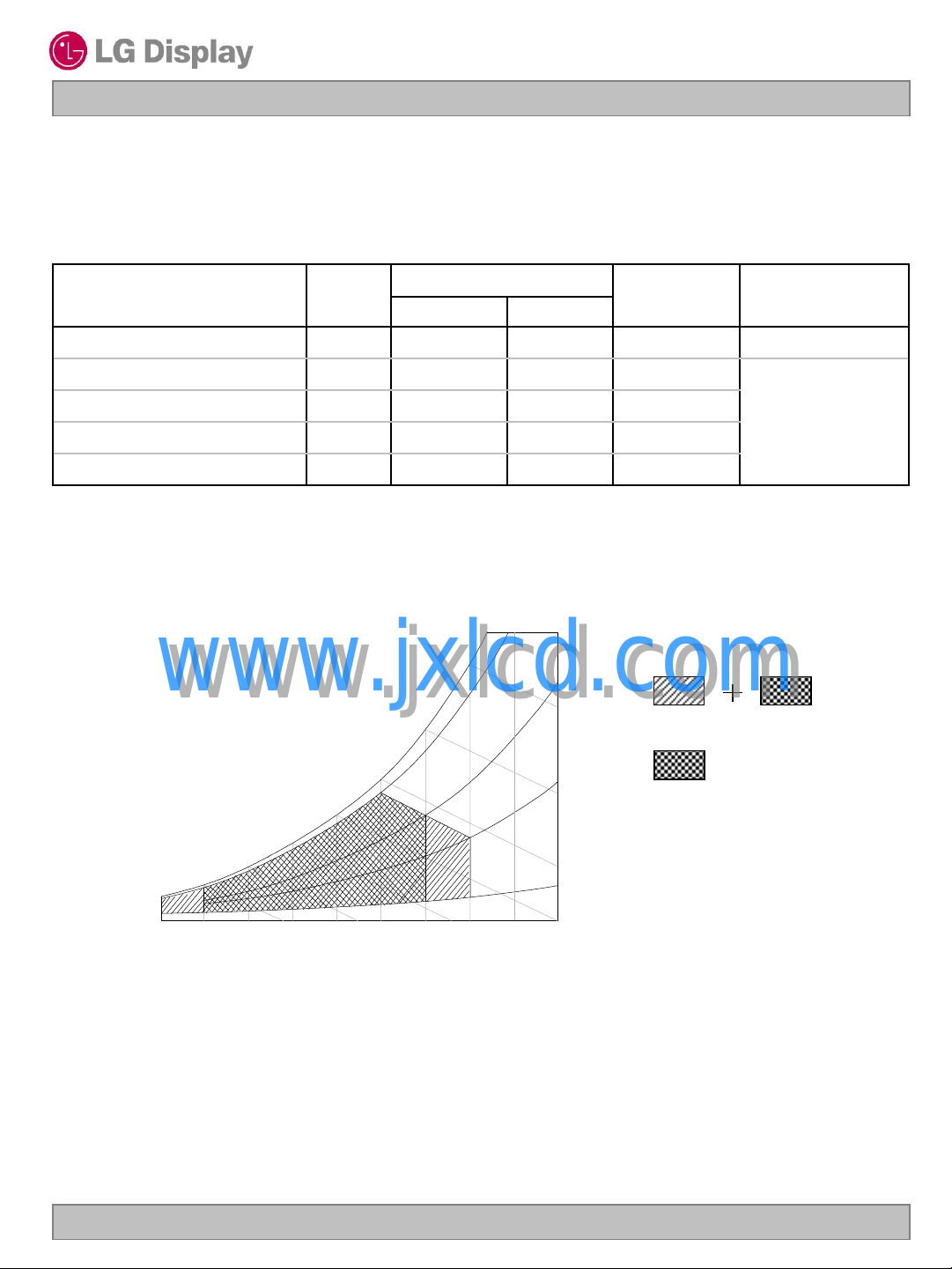
Note.
1. Temperature and relative humidity range are shown in the figure below.
Wet bulb temperature should be 39 °C Max, and no condensation of water.
2. Storage condition is guaranteed under packing condition.
www.jxlcd.com
www.jxlcd.com
Wet Bulb
Temperature [C]
10
0
VLCD -0.3 14 Vdc at 25 2°C
TOP 0 50
TST -20 60
HOP 10 90 %RH
HST 10 90 %RH
50
40
30
20
Values
Min Max
90%
60
60%
40%
Humidity [(%)RH]
10%
Units Notes
°C
°C
1
Storage
Operation
10 20 30 40 50 60 70 800-20
Dry Bulb Temperature [C]
[ Figure 2 ] Temperature and relative humidity
Ver. 1.0 January. 13 . 2011
6 / 35

LM215WF3
Liquid Crystal Display
Product Specification
3. Electrical Specifications
3-1. Electrical Characteristics
It requires two power inputs. One is employed to power the LCD electronics and to drive the TFT array and
liquid crystal. The second input power for the WLED.
Table 2-1. ELECTRICAL CHARACTERISTICS
Parameter Symbol
MODULE :
Power Supply Input Voltage VLCD 11.4 12.0 12.6 Vdc
Permissive Power Input Ripple VRF - - 400 mV
Power Supply Input Current ILCD
Power Consumption
Rush current IRUSH - - 3.0 A 3
Note.
1. The specified current and power consumption are under the V
2. The current is specified at the maximum current pattern.
3. The duration of rush current is about 2ms and rising time of power Input is 1ms(min.)
www.jxlcd.com
www.jxlcd.com
whereas mosaic pattern(8 x 6) is displayed and fVis the frame frequency.
White : 255Gray
Black : 0Gray
PLCD 4.64 5.57 Watt 1
PLCD 6.24 7.50 Watt 2
Min Typ Max
310 387 464 mA 1
416 520 624 mA 2
Values
=12.0V, 25 2°C,fV=60Hz condition
LCD
Maximum current pattern
Unit Notes
Mosaic Pattern(8 x 6)
Ver. 1.0 January. 13 . 2011
White Pattern
7 / 35
Product Specification
Table 2-2. LED Bar ELECTRICAL CHARACTERISTICS
LM215WF3
Liquid Crystal Display
Items Symbol
LED String Voltage V
LED String Power P
BL Power P
LED Life Time LED_LT 30K - Hrs
LED Junction Temperature Tj 150
LED driver design guide
: The design of the LED driver must have specifications for the LED in LCD Assembly.
The performance of the LED in LCM, for example life time or brightness, is extremely influenced by
the characteristics of the LED driver.
So all the parameters of an LED driver should be carefully designed and output current should be
Constant current control.
Please control feedback current of each string individually to compensate the current variation
among the strings of LEDs.
When you design or order the LED driver, please make sure unwanted lighting caused by
the mismatch of the LED and the LED driver (no lighting, flicker, etc) never occurs.
When you confirm it, the LCD module should be operated in the same condition as installed in
your instrument.
www.jxlcd.com
www.jxlcd.com
S
S
BL
Min Typ Max
49.6 52.8 56.0 Vrms
17.36 18.48 19.60 W
- 36.96 39.2 W
Spec
Unit Remark Notes
1,2,3,
7
1,2,3,
4,6,7
1,2,4,
6,7
5,7,8
℃
Ta=25℃, at Duty 100%
of DC 350mA
Ta=25℃, at Duty 100%
of DC 350mA
Ta=25℃, at Duty 100%
of DC 350mA
Tj≤90℃, at Duty 100%
of DC 350mA
- 7,8
1. Specified values are for a single LED bar.
2. The specified current is input LED chip 100% duty current.
3. The specified voltage is input LED string and Bar voltage at typical 350mA 100% duty current.
4. The specified power consumption is input LED bar power consumption at typical 350mA 100% duty current.
5. The LED life time is determined as the time at which brightness of the LED is 70% compared to that of initial
value at the typical LED current on condition of continuous operating at below junction temperature 90°C.
6. The LED power consumption shown above does not include loss of external driver.
The used LED BL current is the LED typical current.
String Power Consumption is calculated with PS= VSx 350mA
BL Power Consumption is calculated with PBL= VSx 350mA x 2(string no.)
7. LED operating DC Forward Current and Junction Temperature must not exceed LED Max Ratings.
8. The LED life time and the maximum rating of LED junction temperature are evaluated at LED package level,
not at liquid crystal module level.
Ver. 1.0 January. 13 . 2011
8 / 35
LM215WF3
Liquid Crystal Display
Product Specification
3-2. Interface Connections
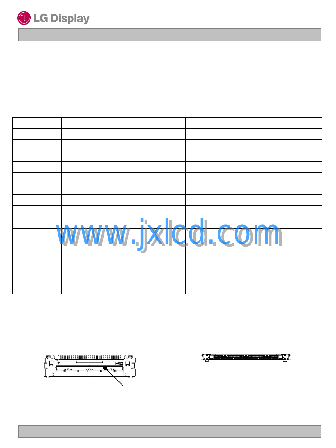
3-2-1. LCD Module
- LCD Connector(CN1) : 20525-030E-01 (I-PEX) or Equivalent
Table 3. MODULE CONNECTOR(CN1) PIN CONFIGURATION
No Symbol Description No Symbol Description
1
2
3
4
5
6
7
8
GND
DDC_SDA
DDC_SCL
GND
I2C_SDA
I2C_SCL
GND
SPDIF
High Speed Ground 16
DDC Data 17
DDC Clock 18 Lane1P
High Speed Ground 19 Lane1N
DDC Data 20
DDC Clock 21 Lane2P
High Speed Ground 22 Lane2N
Audio output from DP RX
23
Lane0N
GND
GND
GND
Component Signal for Main Link 0
High Speed Ground
True Signal for Main Link 1
Component Signal for Main Link 1
High Speed Ground
True Signal for Main Link 2
Component Signal for Main Link 2
High Speed Ground
OPTION-1
9
10
11
12
13
14
15
Note: 1. All GND(ground) pins should be connected together and to Vss which should also be connected to
HPD
GND
AUX_CHN Component Signal for Auxiliary Channel
AUX_CHP True Signal for Auxiliary Channel
GND
Lane0P
the LCD’s metal frame.
Logic (N.C)
Hot Plug Detect Signal
www.jxlcd.com
www.jxlcd.com
High Speed Ground 26
High Speed Ground 29 VSYNC
True Signal for Main Link 0 30
1
20525-030E-01 (I-PEX)
30
24 Lane3P True Signal for Main Link 3
25 Lane3N
GND
27 VIDEO_ON
28 OPTION-2
GND
Component Signal for Main Link 3
High Speed Ground
Video status from DP RX
Logic (N.C)
Vertical Frame Sync.
High Speed Ground
#1
Rear view of LCM
#30
[ Figure 3 ] User Connector diagram
Ver. 1.0 January. 13 . 2011
9 / 35
Product Specification
3-2-2. User Connector
- LCD Connector(CN2) : 53780-8606 (Manufactured by Molex) or Equivalent
Table 4. LCM POWER CONNECTOR(CN2) PIN CONFIGURATION
Pin Symbol Description NOTES
LM215WF3
Liquid Crystal Display
1 GND
2 GND
3 GND
4 VLCD 12V for LCM main power
5
6
Note : 1) NC : No Connection
#1 #6
www.jxlcd.com
www.jxlcd.com
VLCD 12V for LCM main power
VLCD 12V for LCM main power
53780-8606
[ Figure 3-1 ] User Connector diagram
GROUND
GROUND
GROUND
#1 #6
Rear view of LCM
- LCD Connector(CN6) : 53780-8604 (Manufactured by Molex) or Equivalent
Table 4-1. Thermal sensor CONNECTOR(CN6) PIN CONFIGURATION
Pin Symbol Description NOTES
1 DXP Positive connection to remote temperature sensor.
2 DXN Negative connection to remote temperature sensor.
3 GND Ground
4 VSYNCM VSYNCM for synchronized LED Driver
Ver. 1.0 January. 13 . 2011
10 / 35

Product Specification
3-2-3. Backlight Interface
Driver connector: H401K-D06N-12B (Manufactured by E&T)
Mating Connector: 4530K-F06N-01R (Manufactured by E&T)
Table 5. LED DRIVER CONNECTOR PIN CONFIGURATION
Pin Symbol Description NOTES
LM215WF3
Liquid Crystal Display
1
2
3
4
5
6
www.jxlcd.com
www.jxlcd.com
LED1-
LED2+
NC
LED1+
LED2-
NC
LED channel 1 cathode – Left bar
LED channel 2 Anode – Left bar
NC
LED channel 1 Anode – Right bar
LED channel 2 cathode – Right bar
NC
NC/ 2- / 1+/ NC/ 2+ /1
6
1
To right side
[ Figure 4 ] LED Driver Connector Pin
Ver. 1.0 January. 13 . 2011
To left side
11 / 35
 Loading...