

LG LM-201WE3-TLF8 Service manual
Product Specification
SPECIFICATION
LM201WE3
Liquid Crystal Display
FOR
APPROVAL
)
(
(
Preliminary Specification
●
)
Final Specification
BUYER
MODEL
www.jxlcd.com
www.jxlcd.com
APPROVED BY
SIGNATURE
DATE
20.1” WSXGA+ TFT LCDTitle
LG. Display Co., Ltd.SUPPLIER
LM201WE3*MODEL
TLF8SUFFIX
*When you obtain standard approval,
please use the above model name without suffix
APPROVED BY
SIGNATURE
DATE
/
/
/
Please return 1 copy for your confirmation with
your signature and comments.
Ver. 0.0 Non.10. 2008
Hans. Kim / G. Manager
REVIEWED BY
D.I. Jung / Manager
PREPARED BY
S.H. Kim / Engineer
MNT Products Engineering Dept.
LG. Display Co., Ltd
1 / 32
Product Specification
Contents
LM201WE3
Liquid Crystal Display
ITEMNo
COVER
CONTENTS
RECORD OF REVISIONS
GENERAL DESCRIPTION1
ABSOLUTE MAXIMUM RATINGS2
ELECTRICAL SPECIFICATIONS3
ELECTRICAL CHARACTREISTICS 3-1
INTERFACE CONNECTIONS 3-2
SIGNAL TIMING SPECIFICATIONS 3-3
SIGNAL TIMING WAVEFORMS 3-4
COLOR INPUT DATA REFERNECE 3-5
POWER SEQUENCE 3-6
www.jxlcd.com
www.jxlcd.com
OPTICAL SFECIFICATIONS4
MECHANICAL CHARACTERISTICS5
Page
1
2
3
4
5
6
6
9
13
14
15
16
17
22
RELIABILITY6
INTERNATIONAL STANDARDS7
SAFETY 7-1
EMC 7-2
PACKING8
DESIGNATION OF LOT MARK 8-1
PACKING FORM 8-2
PRECAUTIONS9
EDID DATA FOR LM201WE3-TLF810
Ver. 0.0 Non.10. 2008
25
26
26
26
27
27
27
28
30
2 / 32
Product Specification
RECORD OF REVISIONS
Preliminary Specification of LM201WE3-TLF8-Non. 10. 20080.0
LM201WE3
Liquid Crystal Display
DESCRIPTIONPageRevision DateRevision No
www.jxlcd.com
www.jxlcd.com
Ver. 0.0 Non.10. 2008
3 / 32
LM201WE3
Liquid Crystal Display
Product Specification
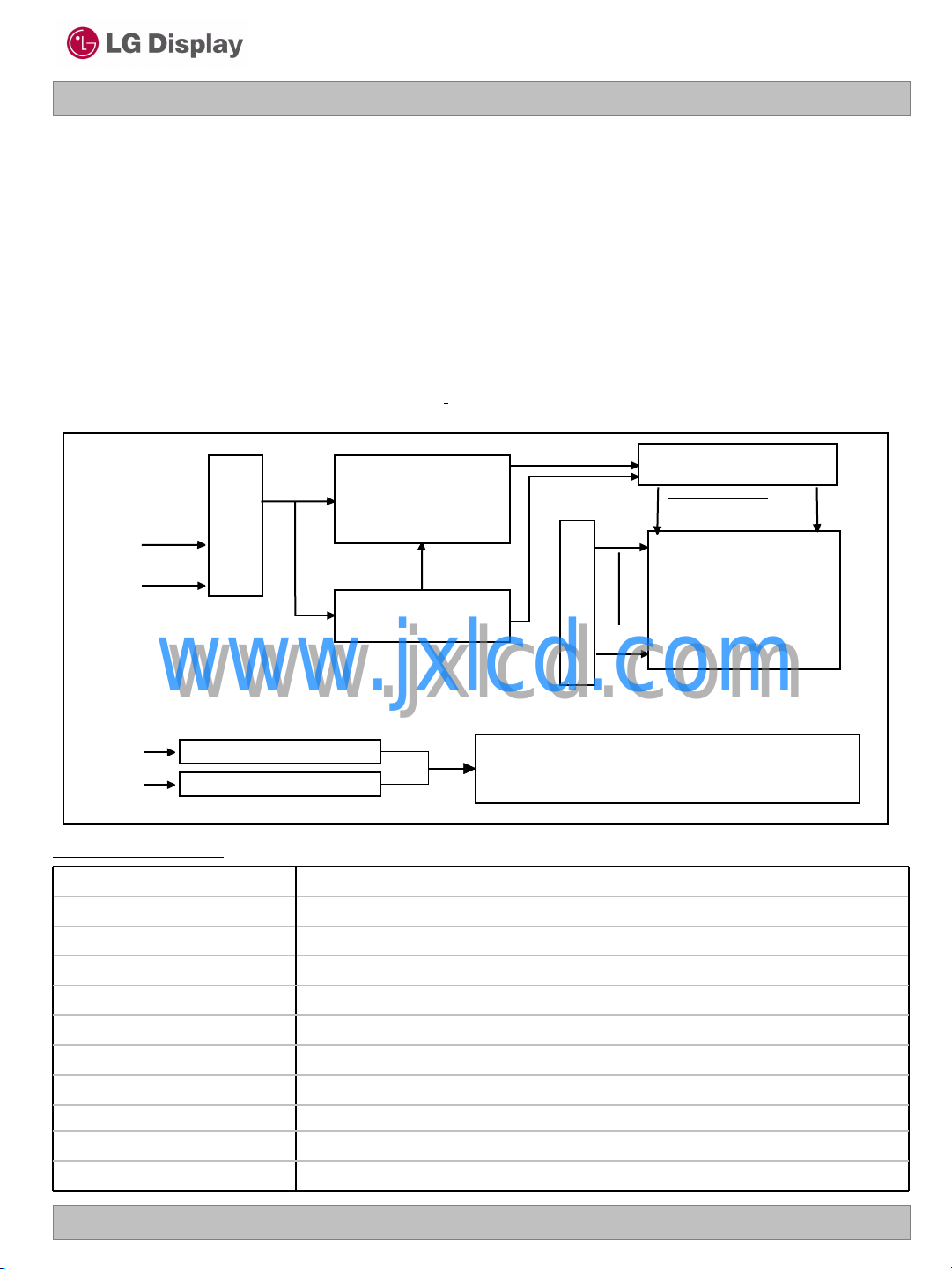
1. General Description
LM201WE3 is a Color Active Matrix Liquid Crystal Display with an integral Cold Cathode Fluorescent
Lamp(CCFL) backlight system. The matrix employs a-Si Thin Film Transistor as the active element.
It is a transmissive type display operating in the normally white mode. It has a 20.1 inch diagonally measured
active display area with WSXGA+ resolution (1050 vertical by 1680 horizontal pixel array)
Each pixel is divided into Red, Green and Blue sub-pixels or dots which are arranged in vertical stripes.
Gray scale or the brightness of the sub-pixel color is determined with a 8-bit gray scale signal for each dot,
thus, presenting a palette of more than 16,7M colors with A-FRC(Advanced Frame Rate Control).
It has been designed to apply the 8Bit 2 port LVDS interface.
It is intended to support displays where high brightness, super wide viewing angle,
high color saturation, and high color are important.
RGB, Dclk, DE
Hsync, Vsync
(LVDS 2 port)
V
(+5V)
LCD
www.jxlcd.com
V
Lamp
V
Lamp
www.jxlcd.com
CN2(2PIN), 3(2PIN)
CN4(2PIN), 5(2PIN)
General Features
CN1
(30pin)
Timing Control
Block
Power Circuit Block
20.1 inches(511.133mm) diagonal (Aspect ratio 16:10)Active Screen Size
459.4(H) x 296.4 (V) x 14.5(D) mm (Typ.)Outline Dimension
0.258mm x 0.258mmPixel Pitch
1680 horiz. By 1050 vert. Pixels RGB strip arrangementPixel Format
16.7 M colorsColor Depth
300 cd/m2 (5 points Avg.)Luminance, White
Viewing Angle Free ( R/L 160(Typ.), U/D 160(Typ) )Viewing Angle (CR>10)
Total 25.21 Watt(Typ.) (3.91 Watt@VLCD, 21.3 Watt@300cd/[LAMP=7.0mA])Power Consumption
2050 g (Typ.)Weight
Transmissive mode, Normally WhiteDisplay Operating Mode
Hard coating (2H), Glare treatment of the front polarizerSurface Treatment
Source Driver Circuit
Gate Driver circuit
G1
TFT-LCD Panel
(1680 1050 pixels)
G1050
Backlight Assembly(4 CCFL)
S1680S1
Ver. 0.0 Non.10. 2008
4 / 32
LM201WE3
Liquid Crystal Display
Product Specification
2. Absolute Maximum Ratings
The following are maximum values which, if exceeded, may cause faulty operation or damage to the unit.
Table 1. ABSOLUTE MAXIMUM RATINGS
Parameter Notes
Power Input Voltage
Operating Temperature
Storage Temperature
Operating Ambient Humidity
Storage Humidity
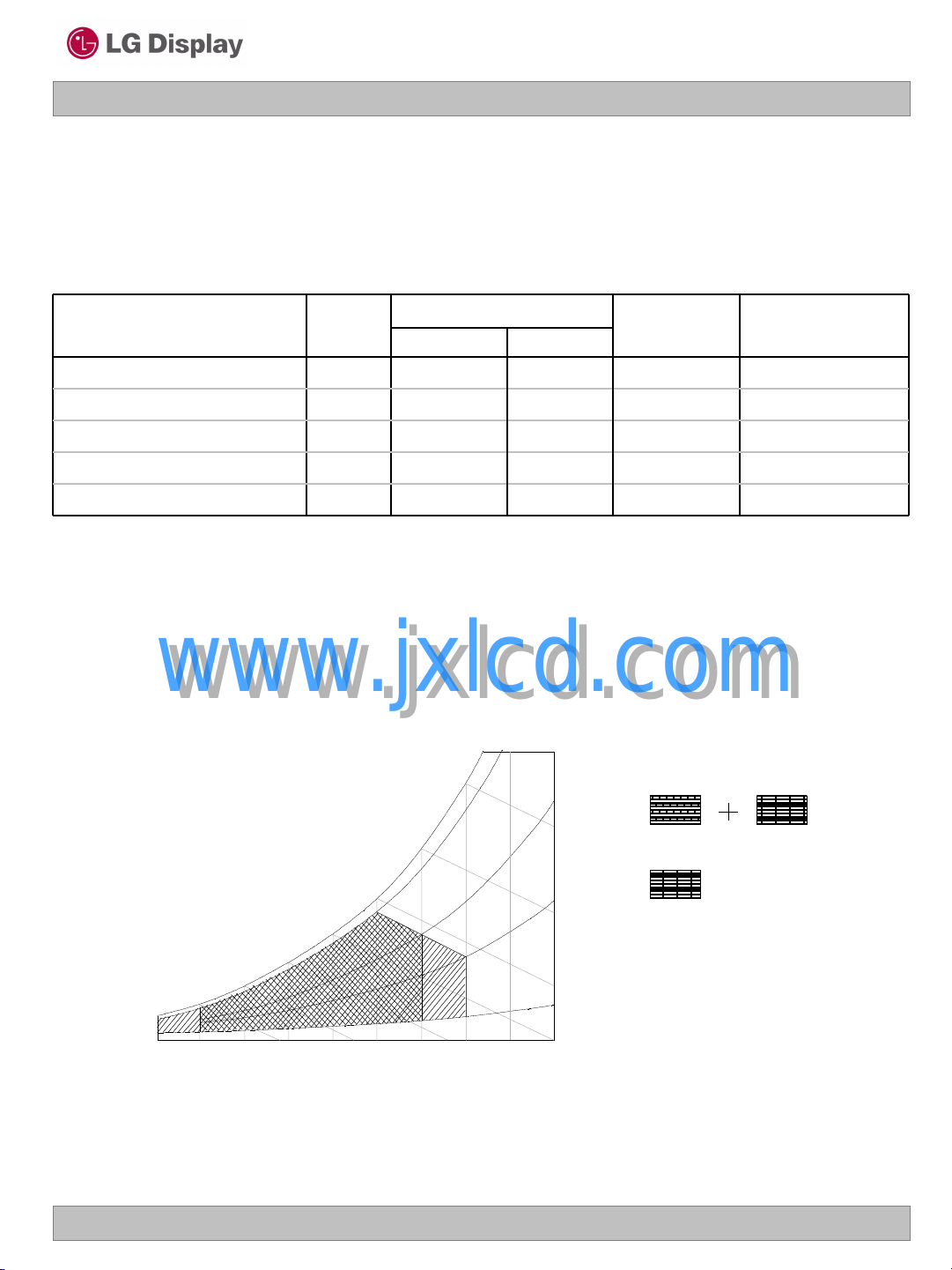
Note : 1. Temperature and relative humidity range are shown in the figure below.
Wet bulb temperature should be 39 °C Max, and no condensation of water.
www.jxlcd.com
www.jxlcd.com
Symbol
Values
MaxMin
500TOP
60-20TST
90%
60
60%
Units
Vdc+5.5-0.3VLCD
°C
°C
at 25 2 °C
1
1
1%RH9010HOP
1%RH9010HST
Wet Bulb
50
Temperature [C]
40
30
20
10
0
10 20 30 40 50 60 70 800-20
Dry Bulb Temperature [C]
Ver. 0.0 Non.10. 2008
40%
10%
Hu
mi
di
ty
[(
%)
RH
]
Storage
Operation
5 / 32
LM201WE3
Liquid Crystal Display
Product Specification
3. Electrical Specifications
3-1. Electrical Characteristics
It requires two power inputs. One is employed to power the LCD electronics and to drive the TFT array and
liquid crystal. The second input power for the CCFL, is typically generated by an inverter. The inverter is an
external unit to the LCDs.
Table 2_1. ELECTRICAL CHARACTERISTICS
Parameter Symbol
MODULE :
ILCD Power Supply Input Current
Note :
1. The specified current and power consumption are under the V
whereas mosaic pattern(8 x 6) is displayed and fV is the frame frequency.
2. The current is specified at the maximum current pattern.
3. The duration of rush current is about 2ms and rising time of power Input is 500us 20%.(min.).
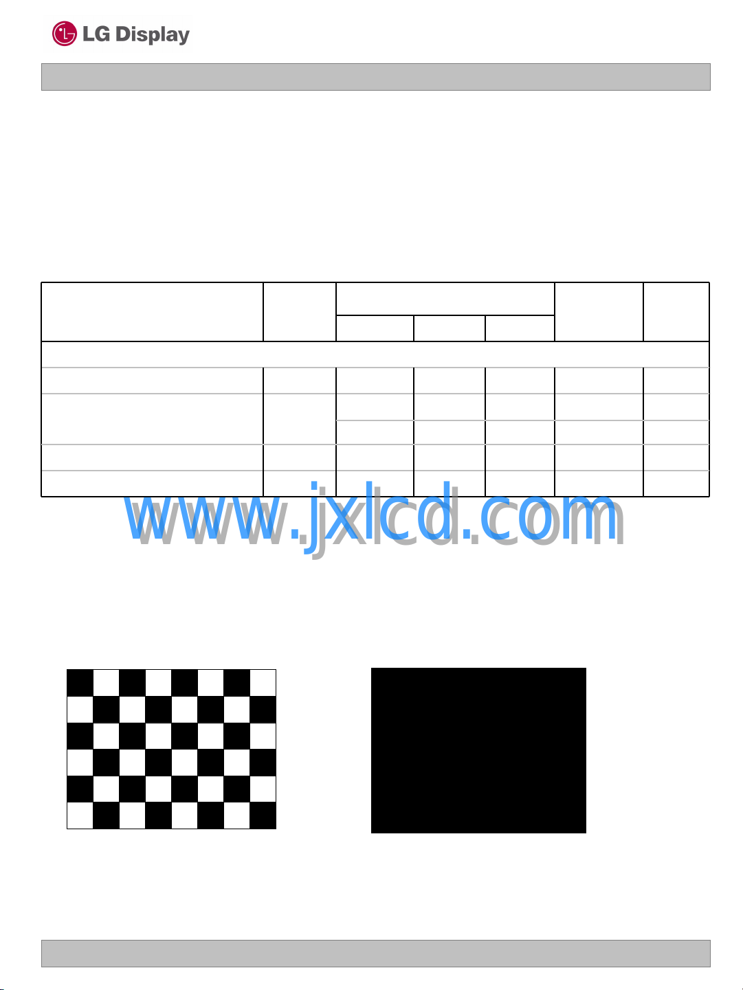
White : 255Gray
Black : 0Gray
www.jxlcd.com
www.jxlcd.com
Maximum current pattern
Values
MaxTypMin
Vdc5.55.04.5VLCD Power Supply Input Voltage
=5.0V, 25 2°C,fV=60Hz condition
LCD
NotesUnit
1mA8997812mA12699761Watt4.503.91-PLCD Power Consumption
3A3--IRUSH Rush current
Mosaic Pattern(8 x 6)
Ver. 0.0 Non.10. 2008
Black Pattern
6 / 32
Product Specification
Table 2_2. ELECTRICAL CHARACTERISTICS
LM201WE3
Liquid Crystal Display
Parameter Symbol
LAMP :
at 25 °C
at 0 °C
Operating Frequency
Discharge Stabilization Time
Power Consumption
Note : The design of the inverter must have specifications for the lamp in LCD Assembly.
Life Time
the characteristics of the DC-AC inverter. So all the parameters of an inverter should be
designed so as not to produce too much leakage current from high-voltage output of the
inverter.
When you design or order the inverter, please make sure unwanted lighting caused by the mismatch
of the lamp and the inverter (no lighting, flicker, etc) never occurs. When you confirm it,
Assembly should be operated in the same condition as installed in you instrument.
※ Do not attach a conducting tape to lamp connecting wire.
If the lamp wire attach to a conducting tape, TFT-LCD Module has a low luminance and the inverter
has abnormal action. Because leakage current is occurred between lamp wire and conducting tape.
The performance of the Lamp in LCM, for example life time or brightness, is extremely
influenced by
carefully
www.jxlcd.com
www.jxlcd.com
the LCD–
Values
MaxTypMin
920(2.5mA)760(7.0mA)725(8.0mA)VBL Operating Voltage
8.07.02.5IBL Operating Current
1250
1550
RMS
RMS
V
RMS
V
RMS
NotesUnit
1, 2V
1, 3Vs Established Starting Voltage
1, 5Min3Ts
1, 7Hrs50,000
1mA
4kHz706040fBL
6Watt23.4321.3PBL
1. Specified values are for a single lamp.
2. Operating voltage is measured at 25 2°C. The variance of the voltage is 10%.
3. The voltage above VS should be applied to the lamps for more than 1 second for start-up.
(Inverter open voltage must be more than lamp starting voltage.)
Otherwise, the lamps may not be turned on. The used lamp current is the lamp typical
current.
4. Lamp frequency may produce interface with horizontal synchronous frequency and as a
result this may
cause beat on the display. Therefore lamp frequency shall be as away possible from the horizontal
synchronous frequency and from its harmonics in order to prevent interference.
5. Let’s define the brightness of the lamp after being lighted for 5 minutes as 100%.
TS is the time required for the brightness of the center of the lamp to be not less than 95%.
6. The lamp power consumption shown above does not include loss of external inverter.
The used lamp current is the lamp typical current. (PBL = VBL x IBL x N
7. The life is determined as the time at which brightness of the lamp is 50% compared to that
of initial
value at the typical lamp current on condition of continuous operating at 25 2°C.
Ver. 0.0 Non.10. 2008
Lamp
)
7 / 32
LM201WE3
Liquid Crystal Display
Product Specification
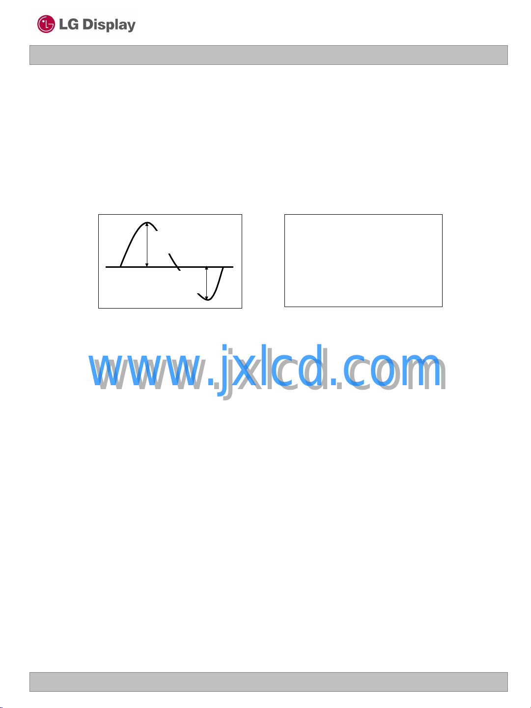
8. The output of the inverter must have symmetrical(negative and positive) voltage waveform
and
symmetrical current waveform (Unsymmetrical ratio is less than 10%). Please do not use the inverter
which has unsymmetrical voltage and unsymmetrical current and spike wave.
Requirements for a system inverter design, which is intended to have a better display performance, a
better power efficiency and a more reliable lamp, are following.
It shall help increase the lamp lifetime and reduce leakage current.
a. The asymmetry rate of the inverter waveform should be less than 10%.
b. The distortion rate of the waveform should be within √2 ±10%.
* Inverter output waveform had better be more similar to ideal sine wave.
* Asymmetry rate:
I p
| I p – I –p | / I
x 100%
rms
I -p
9. The inverter which is combined with this LCM, is highly recommended to connect coupling(ballast)
condenser at the high voltage output side. When you use the inverter which has not coupling(ballast)
condenser, it may cause abnormal lamp lighting because of biased mercury as time goes.
10.In case of edgy type back light with over 4 parallel lamps, input current and voltage wave form should
be synchronized
www.jxlcd.com
www.jxlcd.com
* Distortion rate
I p (or I –p) / I
rms
Ver. 0.0 Non.10. 2008
8 / 32
Product Specification
3-2. Interface Connections
─LCD Connector(CN1) : FI-XB30SRL-HF11 (Manufactured by JAE)
─Mating Connector : FI-X30C2L (Manufactured by JAE) or equivalent.
Table 3. MODULE CONNECTOR(CN1) PIN CONFIGURATION
LM201WE3
Liquid Crystal Display
Pin No
1
2
3
4
5
6
7
8
9
10
11
12
13
14
15
16
17
18
19
20
21
22
23
24
25
26
27
28
29
30
Symbol Description
FR0M
FR0P
FR1M
FR1P
FR2M
FR2P
GND
FCLKINM
FCLKINP
FR3M
FR3P
SR0M
SR0P
GND
SR1M
SR1P
GND
www.jxlcd.com
www.jxlcd.com
SR2M
SR2P
SCLKINM
SCLKINP
SR3M
SR3P
GND
CLK_EDID
DATA_EDID
V_EDID
VLCD
VLCD
VLCD
Minus signal of odd channel 0 (LVDS)
Plus signal of odd channel 0 (LVDS)
Minus signal of odd channel 1 (LVDS)
Plus signal of odd channel 1 (LVDS)
Minus signal of odd channel 2 (LVDS)
Plus signal of odd channel 2 (LVDS)
Ground
Minus signal of odd clock channel (LVDS)
Plus signal of odd clock channel (LVDS)
Minus signal of odd channel 3 (LVDS)
Plus signal of odd channel 3 (LVDS)
Minus signal of even channel 0 (LVDS)
Plus signal of even channel 0 (LVDS)
Ground
Minus signal of even channel 1 (LVDS)
Plus signal of even channel 1 (LVDS)
Ground
Minus signal of even channel 2 (LVDS)
Plus signal of even channel 2 (LVDS)
Minus signal of even clock channel (LVDS)
Plus signal of even clock channel (LVDS)
Minus signal of even channel 3 (LVDS)
Plus signal of even channel 3 (LVDS)
Ground
EEPROM for CLK_EDID
EEPROM for DATA_EDID
EEPROM for V_EDID (3.3V)
Power Supply +5.0V
Power Supply +5.0V
Power Supply +5.0V
First data
Second data
Note: 1. All GND(ground) pins should be connected together and to Vss which should also be
connected to
the LCD’s metal frame.
2. All VLCD (power input) pins should be connected together.
3. Input Level of LVDS signal is based on the IEA 664 Standard.
Ver. 0.0 Non.10. 2008
9 / 32
Product Specification
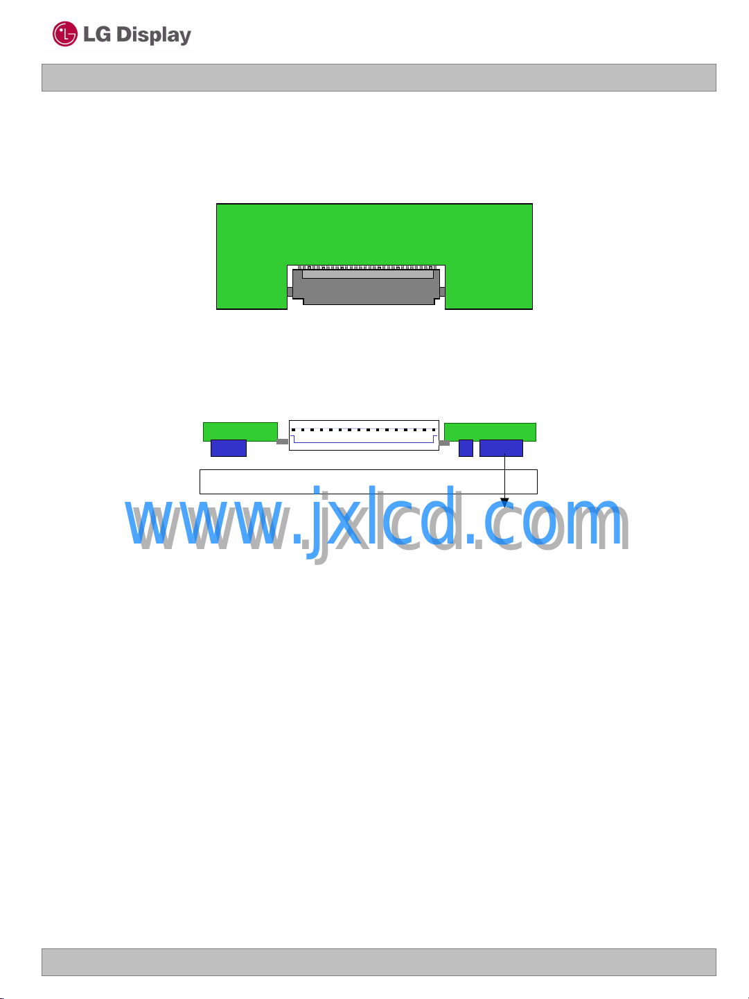
User Connector Diagram
120
FI-XB30SRL-HF11 (JAE)
Input connector
#1 #30
LM201WE3
Liquid Crystal Display
#30#1
PCB
Back Light
Rear view of LCM
www.jxlcd.com
www.jxlcd.com
Components
Ver. 0.0 Non.10. 2008
10 / 32
 Loading...