

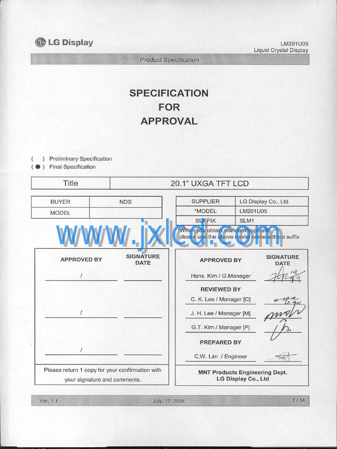
Product Specification
SPECIFICATION
LM201U05
Liquid Crystal Display
FOR
APPROVAL
)
(
(
Preliminary Specification
●
)
Final Specification
MODEL
www.jxlcd.com
www.jxlcd.com
APPROVED BY
NDSBUYER
SIGNATURE
DATE
20.1” UXGA TFT LCDTitle
LG Display Co., Ltd.SUPPLIER
LM201U05*MODEL
SLM1SUFFIX
*When you obtain standard approval,
please use the above model name without suffix
APPROVED BY
SIGNATURE
DATE
/
/
/
Please return 1 copy for your confirmation with
your signature and comments.
Ver. 1.1 July. 17. 2008
Hans. Kim / G.Manager
REVIEWED BY
C. K. Lee / Manager [C]
J. H. Lee / Manager [M]
G.T. Kim / Manager [P]
PREPARED BY
C.W. Lim / Engineer
MNT Products Engineering Dept.
LG Display Co., Ltd
1 / 34

Product Specification
Contents
LM201U05
Liquid Crystal Display
ITEMNo
COVER
CONTENTS
RECORD OF REVISIONS
GENERAL DESCRIPTION1
ABSOLUTE MAXIMUM RATINGS2
ELECTRICAL SPECIFICATIONS3
ELECTRICAL CHARACTREISTICS 3-1
INTERFACE CONNECTIONS 3-2
SIGNAL TIMING SPECIFICATIONS 3-3
SIGNAL TIMING WAVEFORMS 3-4
COLOR INPUT DATA REFERNECE 3-5
POWER SEQUENCE 3-6
www.jxlcd.com
www.jxlcd.com
OPTICAL SFECIFICATIONS4
MECHANICAL CHARACTERISTICS5
Page
1
2
3
4
5
6
6
9
16
17
18
19
20
25
RELIABILITY6
INTERNATIONAL STANDARDS7
SAFETY 7-1
EMC 7-2
ENVIRONMENT 7-3
PACKING8
DESIGNATION OF LOT MARK 8-1
PACKING FORM 8-2
PALLET FORM 8-3
PRECAUTIONS9
Ver. 1.1 July. 17. 2008
28
29
29
29
29
30
30
31
32
33
2 / 34
Product Specification
RECORD OF REVISIONS
Preliminary Specification-Apr. 02. 20080.0
Final specification-Jun. 02. 20081.0
Change CN1 specification10
Change CNTs order15
Updated GTG(max) spec, TCO’03 Spec & Comment20,22
Updated Outline Dimension specification 25
Updated the Rear view Drawing27
Updated Vibration Test specification28
Changed the RoHS sentence29
Updated Packing Form, Pallet Form30,31, 32
Updated Packing Form31July. 17. 20081.1
LM201U05
Liquid Crystal Display
DESCRIPTIONPageRevision DateRevision No
www.jxlcd.com
www.jxlcd.com
Ver. 1.1 July. 17. 2008
3 / 34
LM201U05
Liquid Crystal Display
Product Specification
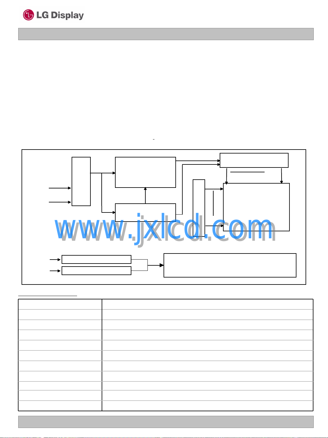
1. General Description
LM201U05-SLM1 is a Color Active Matrix Liquid Crystal Display with an integral Cold Cathode Fluorescent
Lamp(CCFL) backlight system. The matrix employs a-Si Thin Film Transistor as the active element.
It is a transmissive type display operating in the normally black mode. It has a 20.1 inch diagonally measured
active display area with UXGA resolution (1200 vertical by 1600 horizontal pixel array)
Each pixel is divided into Red, Green and Blue sub-pixels or dots which are arranged in vertical stripes.
Gray scale or the brightness of the sub-pixel color is determined with a 8-bit gray scale signal for each dot,
thus, presenting a palette of more than 16,7M(True) colors.
It has been designed to apply the 8Bit 2 port LVDS interface.
It is intended to support displays where high brightness, super wide viewing angle,
high color saturation, and high color are important.
RGB, Dclk, DE
Hsync, Vsync
(LVDS 2 port)
V
(+20V)
LCD
www.jxlcd.com
V
Lamp
V
Lamp
www.jxlcd.com
CN2(5PIN), 3(2PIN)
CN4(2PIN), 5(5PIN)
General Features
CN1
(30pin)
Timing Control
Block
Power Circuit Block
20.1 inches(510.54mm) diagonal Active Screen Size
432.0(H) x 331.5(V) x 25.0(D) mm(Typ.)Outline Dimension
0.255mm x 0.255mmPixel Pitch
1600 horizontal By 1200 vertical Pixels RGB stripe arrangementPixel Format
8bit, 16,7 M colorsColor Depth
300 cd/m2 (Center 1 point, Typ.)Luminance, White
Viewing Angle Free ( R/L 178(Typ.), U/D 178(Typ) )Viewing Angle (CR>10)
Total 35.38 Watt(Typ.) (5.98 Watt@VLCD, 29.4 Watt@300cd/[LAMP=7mA])Power Consumption
3200 g (Typ.)Weight
Transmissive mode, normally blackDisplay Operating Mode
Hard coating (3H), Anti-glare treatment of the front polarizerSurface Treatment
Source Driver Circuit
Gate Driver circuit
G1
TFT-LCD Panel
(1600 1200 pixels)
G1200
Backlight Assembly(6 CCFL)
S1600S1
Ver. 1.1 July. 17. 2008
4 / 34

LM201U05
Liquid Crystal Display
Product Specification
2. Absolute Maximum Ratings
The following are maximum values which, if exceeded, may cause faulty operation or damage to the unit.
Table 1. ABSOLUTE MAXIMUM RATINGS
Parameter Notes
Power Input Voltage
Operating Temperature
Storage Temperature
Operating Ambient Humidity
Storage Humidity
Note : 1. Temperature and relative humidity range are shown in the figure below.
Wet bulb temperature should be 39 °C Max, and no condensation of water.
www.jxlcd.com
www.jxlcd.com
Symbol
Values
MaxMin
500TOP
60-20TST
90%
60
60%
Units
Vdc23.0-0.3VLCD
°C
°C
at 25 2 °C
1
1
1%RH9010HOP
1%RH9010HST
Wet Bulb
50
Temperature [C]
40
30
20
10
0
10 20 30 40 50 60 70 800-20
Dry Bulb Temperature [C]
Ver. 1.1 July. 17. 2008
40%
10%
Hu
mi
di
ty
[(
%)
RH
]
Storage
Operation
5 / 34
LM201U05
Liquid Crystal Display
Product Specification
3. Electrical Specifications
3-1. Electrical Characteristics
It requires two power inputs. One is employed to power the LCD electronics and to drive the TFT array and
liquid crystal. The second input power for the CCFL, is typically generated by an inverter. The inverter is an
external unit to the LCDs.
Table 2_1. ELECTRICAL CHARACTERISTICS
Parameter Symbol
MODULE :
ILCD Power Supply Input Current
Note :
1. The specified current and power consumption are under the V
whereas mosaic pattern(8 x 6) is displayed and fV is the frame frequency.
2. The current is specified at the maximum current pattern.
3. The duration of rush current is about 2ms and rising time of power Input is 1ms(min.).
White : 255Gray
Black : 0Gray
www.jxlcd.com
www.jxlcd.com
Maximum current pattern
Values
LCD
MaxTypMin
Vdc19V18V17VVLCD Power Supply Input Voltage
=18.0V, 25 2°C,fV=60Hz condition
NotesUnit
1mA3823322mA4814191Watt6.885.98-PLCD Power Consumption
3A3--IRUSH Rush current
Mosaic Pattern(8 x 6)
Ver. 1.1 July. 17. 2008
White Pattern
6 / 34

Product Specification
Table 2_2. ELECTRICAL CHARACTERISTICS
LM201U05
Liquid Crystal Display
Parameter Symbol
LAMP :
at 25 °C
at 0 °C
Operating Frequency
Discharge Stabilization Time
Power Consumption
Note : The design of the inverter must have specifications for the lamp in LCD Assembly.
Life Time
the characteristics of the DC-AC inverter. So all the parameters of an inverter should be
designed so as not to produce too much leakage current from high-voltage output of the
inverter.
When you design or order the inverter, please make sure unwanted lighting caused by the mismatch
of the lamp and the inverter (no lighting, flicker, etc) never occurs. When you confirm it,
Assembly should be operated in the same condition as installed in you instrument.
※ Do not attach a conducting tape to lamp connecting wire.
If the lamp wire attach to a conducting tape, TFT-LCD Module has a low luminance and the inverter
has abnormal action. Because leakage current is occurred between lamp wire and conducting tape.
The performance of the Lamp in LCM, for example life time or brightness, is extremely
influenced by
carefully
www.jxlcd.com
www.jxlcd.com
the LCD–
Values
825(3mA)700670(8.0mA)VBL Operating Voltage
MaxTypMin
8.07.03.0IBL Operating Current
1150
1450
NotesUnit
RMS
RMS
V
RMS
V
RMS
1, 3V
2mA
2, 4Vs Established Starting Voltage
5kHz805040fBL
2, 6Min3--Ts
7Watt32.329.4PBL
2, 8Hrs45,000
1. It is only reference voltage in LCM.
2. Specified values are for a single lamp.
3. Operating voltage is measured at 25 2°C.
4. The voltage above VS should be applied to the lamps for more than 1 second for start-up.
(Inverter open voltage must be more than lamp starting voltage.)
Otherwise, the lamps may not be turned on. The used lamp current is the lamp typical
current.
5. Lamp frequency may produce interface with horizontal synchronous frequency and as a
result this may
cause beat on the display. Therefore lamp frequency shall be as away possible from the horizontal
synchronous frequency and from its harmonics in order to prevent interference.
6. Let’s define the brightness of the lamp after being lighted for 5 minutes as 100%.
TS is the time required for the brightness of the center of the lamp to be not less than 95%.
7. The lamp power consumption shown above does not include loss of external inverter.
The used lamp current is the lamp typical current. (PBL = VBL x IBL x N
8. The life is determined as the time at which brightness of the lamp is 50% compared to that
of initial
value at the typical lamp current on condition of continuous operating at 25 2°C.
Ver. 1.1 July. 17. 2008
Lamp
)
7 / 34

LM201U05
Liquid Crystal Display
Product Specification
9. The output of the inverter must have symmetrical(negative and positive) voltage waveform
and
symmetrical current waveform (Unsymmetrical ratio is less than 10%). Please do not use the inverter
which has unsymmetrical voltage and unsymmetrical current and spike wave.
Requirements for a system inverter design, which is intended to have a better display performance, a
better power efficiency and a more reliable lamp, are following.
It shall help increase the lamp lifetime and reduce leakage current.
a. The asymmetry rate of the inverter waveform should be less than 10%.
b. The distortion rate of the waveform should be within √2 ±10%.
* Inverter output waveform had better be more similar to ideal sine wave.
* Asymmetry rate:
I p
| I p – I –p | / I
x 100%
rms
I -p
10. The inverter which is combined with this LCM, is highly recommended to connect coupling(ballast)
condenser at the high voltage output side. When you use the inverter which has not coupling(ballast)
condenser, it may cause abnormal lamp lighting because of biased mercury as time goes.
11.In case of edgy type back light with over 4 parallel lamps, input current and voltage wave form should
be synchronized
www.jxlcd.com
www.jxlcd.com
* Distortion rate
I p (or I –p) / I
rms
Ver. 1.1 July. 17. 2008
8 / 34
Product Specification
3-2. Interface Connections
─LCD Connector(CN1) : AL230F-ALG1D-P (Manufactured by P-TWO) or IS100-L30R-C23
(Manufactured by UJU) or Equivalent
─Mating Connector : FI-X30M (Manufactured by JAE) or Equivalent
Table 3. MODULE CONNECTOR(CN1) PIN CONFIGURATION
Pin DescriptionSymbol
LM201U05
Liquid Crystal Display
1
2
3
4
5
6
7
8
9
10
11
12
13
14
15
16
17
18
19
20
21
22
23
24
25
26
27
28
29
30
Vcc
Vcc
Vcc
Vcc
NC
NC
SR3P
SR3M
SCLKINP
SCLKINM
SR2P
SR2M
SR1P
SR1M
SR0P
SR0M
www.jxlcd.com
www.jxlcd.com
GND
GND
FR3P
FR3M
FCLKINP
FCLKINM
FR2P
FR2M
FR1P
FR1M
FR0P
FR0M
GND
GND
Supply voltage for LCD module
Supply voltage for LCD module
Supply voltage for LCD module
Supply voltage for LCD module
NC (No Connection)
NC (No Connection)
Plus signal of even channel 3 (LVDS)
Minus signal of even channel 3 (LVDS)
Plus signal of even clock channel (LVDS)
Minus signal of even clock channel (LVDS)
Plus signal of even channel 2 (LVDS)
Minus signal of even channel 2 (LVDS)
Plus signal of even channel 1 (LVDS)
Minus signal of even channel 1 (LVDS)
Plus signal of even channel 0 (LVDS)
Minus signal of even channel 0 (LVDS)
Ground
Ground
Plus signal of odd channel 3 (LVDS)
Minus signal of odd channel 3 (LVDS)
Plus signal of odd clock channel (LVDS)
Minus signal of odd clock channel (LVDS)
Plus signal of odd channel 2 (LVDS)
Minus signal of odd channel 2 (LVDS)
Plus signal of odd channel 1 (LVDS)
Minus signal of odd channel 1 (LVDS)
Plus signal of odd channel 0 (LVDS)
Minus signal of odd channel 0 (LVDS)
Ground
Ground
Second data
First data
Note: 1. NC: No Connection.
2. All GND(ground) pins should be connected together and to Vss which should also be
connected to
the LCD’s metal frame.
3. All VLCD (power input) pins should be connected together.
4. Input Level of LVDS signal is based on the IEA 664 Standard.
Ver. 1.1 July. 17. 2008
9 / 34

Product Specification
User Connector Diagram
LM201U05
Liquid Crystal Display
#30
AL230F-ALG1D-P ( P-TWO)
www.jxlcd.com
www.jxlcd.com
#1
#30
PCB
Input connector
BackLight
Rear view of LCM
Components
#1
PCB
Ver. 1.1 July. 17. 2008
10 / 34

Liquid Crystal Display
Product Specification
Table 4. REQUIRED SIGNAL ASSIGNMENT FOR Flat Link (TI:SN75LVDS83) Transmitter
Pin # Require SignalPin Name Pin # Require SignalPin Name
1 Power Supply for TTL InputVCC 29 Ground pin for TTLGND
2 TTL Input (R7)D5 30 TTL Input (DE)D26
3 TTL Input (R5)D6 31 TTL Level clock InputTX CLKIN
4 TTL Input (G0)D7 32 Power Down InputPWR DWN
5 Ground pin for TTLGND 33 Ground pin for PLLPLL GND
6 TTL Input (G1)D8 34 Power Supply for PLLPLL VCC
7 TTL Input (G2)D9 35 Ground pin for PLLPLL GND
8 TTL Input (G6)D10 36 Ground pin for LVDSLVDS GND
9 Power Supply for TTL InputVCC 37 Positive LVDS differential data output 3TxOUT3+
10 TTL Input (G7)D11 38 Negative LVDS differential data output 3TxOUT3-
LM201U05
11 TTL Input (G3)D12 39 Positive LVDS differential clock outputTX CLKOUT+
12 TTL Input (G4)D13 40 Negative LVDS differential clock outputTX CLKOUT-
13 Ground pin for TTLGND 41 Positive LVDS differential data output 2TX OUT2+
14 TTL Input (G5)D14 42 Negative LVDS differential data output 2TX OUT2-
15 TTL Input (B0)D15 43 Ground pin for LVDSLVDS GND
16 TTL Input (B6)D16 44 Power Supply for LVDSLVDS VCC
17 Power Supply for TTL InputVCC 45 Positive LVDS differential data output 1TX OUT1+
19 TTL Input (B1)D18
20 TTL Input (B2)D19
22 TTL Input (B3)D20
23 TTL Input (B4)D21
24 TTL Input (B5)D22
25 TTL Input (RSVD)D23
26 Power Supply for TTL InputVCC 54 TTL Input (R2)D2
www.jxlcd.com
www.jxlcd.com
46 Negative LVDS differential data output 1TX OUT1-18 TTL Input (B7)D17
47 Positive LVDS differential data output 0TX OUT0+
48 Negative LVDS differential data output 0TX OUT0-
49 Ground pin for LVDSLVDS GND21 Ground pin for TTL InputGND
50 TTL Input (R6)D27
51 TTL Input (R0)D0
52 TTL Input (R1)D1
53 Ground pin for TTLGND
55 TTL Input (R3)D327 TTL Input (HSYNC)D24
56 TTL Input (R4)D428 TTL Input (VSYNC)D25
Notes : Refer to LVDS Transmitter Data Sheet for detail descriptions.
Ver. 1.1 July. 17. 2008
11 / 34

LVDS Input characteristics
LVDS Data
t
SKEW
LVDS Clock
T
clk
t
SKEW (Fclk
= 1/T
clk
)
1) 85MHz > Fclk ≥ 65MHz : -400 ~ +400
2) 85MHz > Fclk ≥ 65MHz : -600 ~ +600
LVDS +
LVDS -
0V
V
CM
# |VID| = |(LVDS+) – (LVDS-)|
# VCM= {(LVDS+) + (LVDS-)}/2
|VID|
V
IN_MAXVIN_MIN
1. DC Specification
LM201U05
Liquid Crystal Display
Product Specification
NotesUnitMaxMinSymbolDescription
LVDS Common mode Voltage
LVDS Input Voltage Range
www.jxlcd.com
2. AC Specification
LVDS Clock to Data Skew Margin
LVDS Clock to Clock Skew Margin (Even to
Odd)
Maximum deviation
of input clock frequency during SSC
Maximum modulation frequency
of input clock during SSC
www.jxlcd.com
-mV600100|VID|LVDS Differential Voltage
CM
IN
SKEW
SKEW
SKEW_EO
DEV
MOD
600-
- 1/7
+ 1/7t
KHz200-F
85MHz > Fclk ≥ 65MHzps+ 400 400-t
65MHz > Fclk ≥ 25MHz
ps+ 600t
T
clk
%± 3-F
-V1.80.6V
-V2.10.3V
NotesUnitMaxMinSymbolDescription
-
-
-
Ver. 1.1 July. 17. 2008
12 / 34

LVDS Even Data
LVDS Odd Clock
LVDS Even Clock
t
SKEW_EO
T
clk
T
clk
OG0 OR5 OR4 OR3 OR2 OR1 OR0
OB1 OB0 OG5 OG4 OG3 OG2 OG1
DE VSYNC HSYNC OB5 OB4 OB3 OB2
X OB7 OB6 OG7 OG6 OR7 OR6
Current(Nth) CyclePrevious(N-1)th Cycle Next(N+1)th Cycle
RCLK +
RXinO0 +/-
Tclk * 4/7 Tclk * 3/7
Tclk
Tclk * 1/7
MSB R7
R6
R5
R4
R3
R2
R1
R0LSB
EG0 ER5 ER4 ER3 ER2 ER1 ER0
EB1 EB0 EG5 EG4 EG3 EG2 EG1
DE
VSYNC HSYNC
EB5 EB4 EB3 EB2
X EB7 EB6 EG7 EG6 ER7 ER6
* ODD = 1st Pixel
EVEN = 2nd Pixel
RXinO1 +/-
RXinO2 +/-
RXinO3 +/-
RXinE0 +/-
RXinE1 +/-
RXinE2 +/-
RXinE3 +/-
OR3 OR2 OR1 OR0
OG4 OG3 OG2 OG1
OB5 OB4 OB3 OB2
OG7 OG6 OR7 OR6
ER3 ER2 ER1 ER0
EG4 EG3 EG2 EG1
EB5 EB4 EB3 EB2
EG7 EG6 ER7 ER6
OG0 OR5 OR4
OB1 OB0 OG5
DE VSYNC HSYNC
X OB7 OB6
EG0 ER5 ER4
EB1 EB0 EG5
DE
VSYNC HSYNC
X EB7 EB6
Freq.
F
max
F
center
F
min
Product Specification
< Clock skew margin between channel >
LM201U05
Liquid Crystal Display
F
* F
center
DEV
3. Data Format
1) LVDS 2 Port
Ver. 1.1 July. 17. 2008
www.jxlcd.com
www.jxlcd.com
< Spread Spectrum >
< LVDS Data Format >
1
F
MOD
Time
13 / 34

2) LVDS 1 Port
RCLK+
LM201U05
Liquid Crystal Display
Product Specification
RA+/-
RB+/-
RC+/-
RD+/-
R3 R2
G4 G3
B5 B4
G7 G6
Previous (N-1)th Cycle Next(N+1)th Cycle
www.jxlcd.com
www.jxlcd.com
R1 R0
G2 G1
B3 B2
R7 R6
G0 R5 R4 R3 R2 R1 R0
B1 B0 G5 G4 G3 G2 G1
DE VSYNC HSYNC B5 B4 B3 B2
X B7 B6 G7 G6 R7 R6
Current (Nth) Cycle
G0
B1
DE
VSYNC HSYNC
X
R5 R4
B0 G5
B7 B6
Ver. 1.1 July. 17. 2008
14 / 34

LM201U05
Liquid Crystal Display
Product Specification
Table 5. BACKLIGHT CONNECTOR PIN CONFIGURATION(CN2,CN3,CN4,CN5)
The backlight interface connector is a model 1674817-1(CN3/CN4) manufactured by AMP ( or equivalent
BHSR-02VS-1 manufactured by JST) and BHR-05VS-1 (CN2/CN5) manufactured by JST. The mating
connector part number are SM02B-BHSS-1-TB(2pin), SM04(9-E2)B-BHS-1-TB or equivalent. The pin
configuration for the connector is shown in the table below.
Symbol
CN2
5
CN3
CN4
CN5
www.jxlcd.com
www.jxlcd.com
5
Notes: 1. The high voltage power terminal is thick line.
2. The low voltage power terminal is thin line.
HV
HV
NC
LV
LV Power supply for lamp 2(Low voltage side)
HV
LV
HV 1Power supply for lamp 4(High voltage side)1
LV
HV
HV
NC
LV
LV Power supply for lamp 5(Low voltage side)
NC3
NC3
NotesDescriptionPinNo
1Power supply for lamp 1(High voltage side) 1
1Power supply for lamp 2(High voltage side)2
2Power supply for lamp 1(Low voltage side)4
2
1Power supply for lamp 3(High voltage side)1
2Power supply for lamp 3(Low voltage side) 2
2Power supply for lamp 4(Low voltage side)2
1Power supply for lamp 6(High voltage side) 1
1Power supply for lamp 5(High voltage side)2
2Power supply for lamp 6(Low voltage side)4
2
Up Side
Down Side
Ver. 1.1 July. 17. 2008
<BACKLIGHT CONNECTOR DIAGRAM>
Lamp1
Lamp 2
Lamp 3
Lamp 4
Lamp 5
Lamp 6
CN 2
CN 3
CN 4
CN 5
15 / 34
LM201U05
Liquid Crystal Display
Product Specification
3-3. Signal Timing Specifications
This is the signal timing required at the input of the User connector. All of the interface signal timing should be
satisfied with the following specifications for it’s proper operation.
Table 6. Timing Table
Enable
SYMBOL
PeriodDCLK
Frequency
PeriodHsync
Width-Active
PeriodVsync
Frequency
Width-Active
Horizontal ValidData
www.jxlcd.com
www.jxlcd.com
Horizontal Back Porch
Horizontal Front Porch
Horizontal Blank
tCLK
fCLK
tHP
tWH
tVP
fV
tWV
tHV
tHBP
tHFP
-
16.0015.62514.28
70.064.062.5
906860852
161616
125012401230
616059
442
800800800
482420
422016
1066052
ns
tCLK
tHP
Hz
tHP
tCLK
NoteUnitMaxTypMinITEM
2pixel/clkMHz
Vertical Valid
Vertical Back Porch
Vertical Front Porch
Vertical Blank
Notes: Hsync period and Hsync width-active should be even number times of tCLK. If the value is odd number
times of tCLK, display control signal can be asynchronous. In order to operate this LCM a Hsync,
Vsyn, and DE(data enable) signals should be used.
1. The performance of the electro-optical characteristics may be influenced by variance of the vertical
refresh rates.
2. Vsync and Hsync should be keep the above specification.
3. Hsync Period, Hsync Width, and Horizontal Back Porch should be any times of of character
number(8).
4. The polarity of Hsync, Vsync is not restricted.
Ver. 1.1 July. 17. 2008
tVV
tVBP
tVFP
-
120012001200
423224
tHP
444
504030
16 / 34
3-4. Signal Timing Waveforms
LM201U05
Liquid Crystal Display
Product Specification
DCLK
First data
Second data
DE(Data Enable)
www.jxlcd.com
Hsync, Vsync, DE, Data
tCLK
0.5 VCC
Invalid data
Invalid data
Valid data
Pixel 0,0
Valid data
Pixel 1,0
0.7VCC
Pixel 2,0
Pixel 3,0
0.3VCC
Invalid data
Invalid data
www.jxlcd.com
tHP
HSync
DE(Data Enable)
VSync
DE(Data Enable)
Ver. 1.1 July. 17. 2008
tWH
tWV
tHBP tHV
tVP
tVBP
tVV tVFP
tHFP
17 / 34

LM201U05
Liquid Crystal Display
Product Specification
3-5. Color Data Reference
The Brightness of each primary color(red,green,blue) is based on the 8-bit gray scale data input for the color;
the higher the binary input, the brighter the color. The table below provides a reference for color versus data
input.
Table 7. COLOR DATA REFERENCE
Input Color Data
Basic
Color
RED
Color
Black 0 0 0 0 0 0 0 00 0 0 0 0 0 0 00 0 0 0 0 0 0 0
Red (255)
Green (255)
Blue (255)
Cyan
Magenta
Yellow
White
www.jxlcd.com
www.jxlcd.com
MSB LSB
RED
GREEN
MSB LSB
MSB LSB
B7 B6 B5 B4 B3 B2 B1 B0G7 G6 G5 G4 G3 G2 G1 G0R7 R6 R5 R4 R3 R2 R1 R0
BLUE
0 0 0 0 0 0 0 00 0 0 0 0 0 0 01 1 1 1 1 1 1 1
0 0 0 0 0 0 0 01 1 1 1 1 1 1 10 0 0 0 0 0 0 0
1 1 1 1 1 1 1 10 0 0 0 0 0 0 00 0 0 0 0 0 0 0
1 1 1 1 1 1 1 11 1 1 1 1 1 1 10 0 0 0 0 0 0 0
1 1 1 1 1 1 1 10 0 0 0 0 0 0 01 1 1 1 1 1 1 1
0 0 0 0 0 0 0 01 1 1 1 1 1 1 11 1 1 1 1 1 1 1
1 1 1 1 1 1 1 11 1 1 1 1 1 1 11 1 1 1 1 1 1 1
0 0 0 0 0 0 0 00 0 0 0 0 0 0 00 0 0 0 0 0 0 0RED (000) Dark
0 0 0 0 0 0 0 00 0 0 0 0 0 0 00 0 0 0 0 0 0 1RED (001)
............
0 0 0 0 0 0 0 00 0 0 0 0 0 0 01 1 1 1 1 1 1 0RED (254)
0 0 0 0 0 0 0 00 0 0 0 0 0 0 01 1 1 1 1 1 1 1RED (255)
0 0 0 0 0 0 0 00 0 0 0 0 0 0 00 0 0 0 0 0 0 0GREEN (000) Dark
GREEN
BLUE (000) Dark
BLUE
Ver. 1.1 July. 17. 2008
0 0 0 0 0 0 0 00 0 0 0 0 0 0 10 0 0 0 0 0 0 0GREEN (001)
............
0 0 0 0 0 0 0 01 1 1 1 1 1 1 00 0 0 0 0 0 0 0GREEN (254)
0 0 0 0 0 0 0 01 1 1 1 1 1 1 10 0 0 0 0 0 0 0GREEN (255)
0 0 0 0 0 0 0 00 0 0 0 0 0 0 00 0 0 0 0 0 0 0
0 0 0 0 0 0 0 10 0 0 0 0 0 0 00 0 0 0 0 0 0 0BLUE (001)
............
1 1 1 1 1 1 1 00 0 0 0 0 0 0 00 0 0 0 0 0 0 0BLUE (254)
1 1 1 1 1 1 1 10 0 0 0 0 0 0 00 0 0 0 0 0 0 0BLUE (255)
18 / 34
3-6. Power Sequence
LM201U05
Liquid Crystal Display
Product Specification
V
LCD
90%
90%
Power Supply, V
Interface Signal, V
(Digital RGB signal, SCDT
,V
, H
sync
sync
PanelLink Transmitter)
Power Supply for Backlight
Inverter
Table 8. POWER SEQUENCE
LCD
i
, DE, Clock to
www.jxlcd.com
www.jxlcd.com
Parameter
0V
0V
10%
T1
T2 T5 T7
Valid Data
T3
LAMP ON LAMP OFF
Values
T6
T4
10%
LAMP OFF
MaxTypMin
--200T4
Units
ms10--T1
ms50-0.01T2
ms--200T3
ms
ms50-0.01T5
ms--400T7
Notes : 1. Please avoid floating state of interface signal at invalid period.
2. When the interface signal is invalid, be sure to pull down the power supply for LCD V
0V.
3. Lamp power must be turn on after power supply for LCD an interface signal are valid.
Ver. 1.1 July. 17. 2008
to
LCD
19 / 34
LM201U05
Liquid Crystal Display
Product Specification
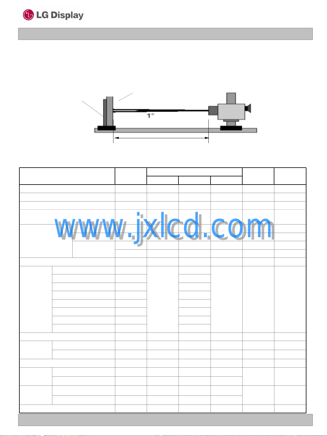
4. Optical Specification
Optical characteristics are determined after the unit has been ‘ON’ and stable for approximately 30 minutes in
a dark environment at 25±2°C. The values specified are at an approximate distance 50cm from the LCD
surface at a viewing angle of and equal to 0 °.
FIG. 1 presents additional information concerning the measurement equipment and method.
Optical Stage(x,y)
LCD Module
50cm
FIG. 1 Optical Characteristic Measurement Equipment and Method
Table 9. OPTICAL CHARACTERISTICS Ta=25 °C, V
Parameter Symbol NotesUnits
Surface Luminance, white
Luminance Variation
Luminance uniformity Angular
dependence (TCO’03)
Rise Time
Response Time
Color Coordinates
Viewing Angle
general
Effective
Ver. 1.1 July. 17. 2008
www.jxlcd.com
RED
GREEN
BLUE
WHITE
Horizontal
Vertical
Horizontal
Vertical
Horizontal
Vertical
Decay Time
www.jxlcd.com
Gray To Gray
WH
WHITE
R
D
GTG_AVR
GTG_MAX
RX
CST_H
CST_V
H
V
GMA_H
GMA_V
-0.03
Values
300250L
6.5-Tr
0.639
0.342RY
0.295GX
0.615GY
0.146BX
0.072BY
0.313WX
0.329WY
178
178
=18.0V, fV=60Hz Dclk=128MHz, IBL=7mA
LCD
MAxTypMin
+0.03
Pritchard 880 or
equivalent
25
-178-
-178-
--
-178-
1800400CRContrast Ratio
2
degree-178-
2cd/m
3%--75
FIG 31.7--
4ms
4ms7.5-Tr
5ms-6-T
5ms-12-T
6Color shift
7degree
8degree
92.2Gray Scale
20 / 34
Liquid Crystal Display
(%)100
)L .... ,L ,(L Maximum
)L .. ,L,Minimum(L
on9on2on1
on9on2on1
WHITE
Product Specification
Notes 1. Contrast Ratio(CR) is defined mathematically as :
Surface Luminance with all white pixels
Contrast Ratio =
Surface Luminance with all black pixels
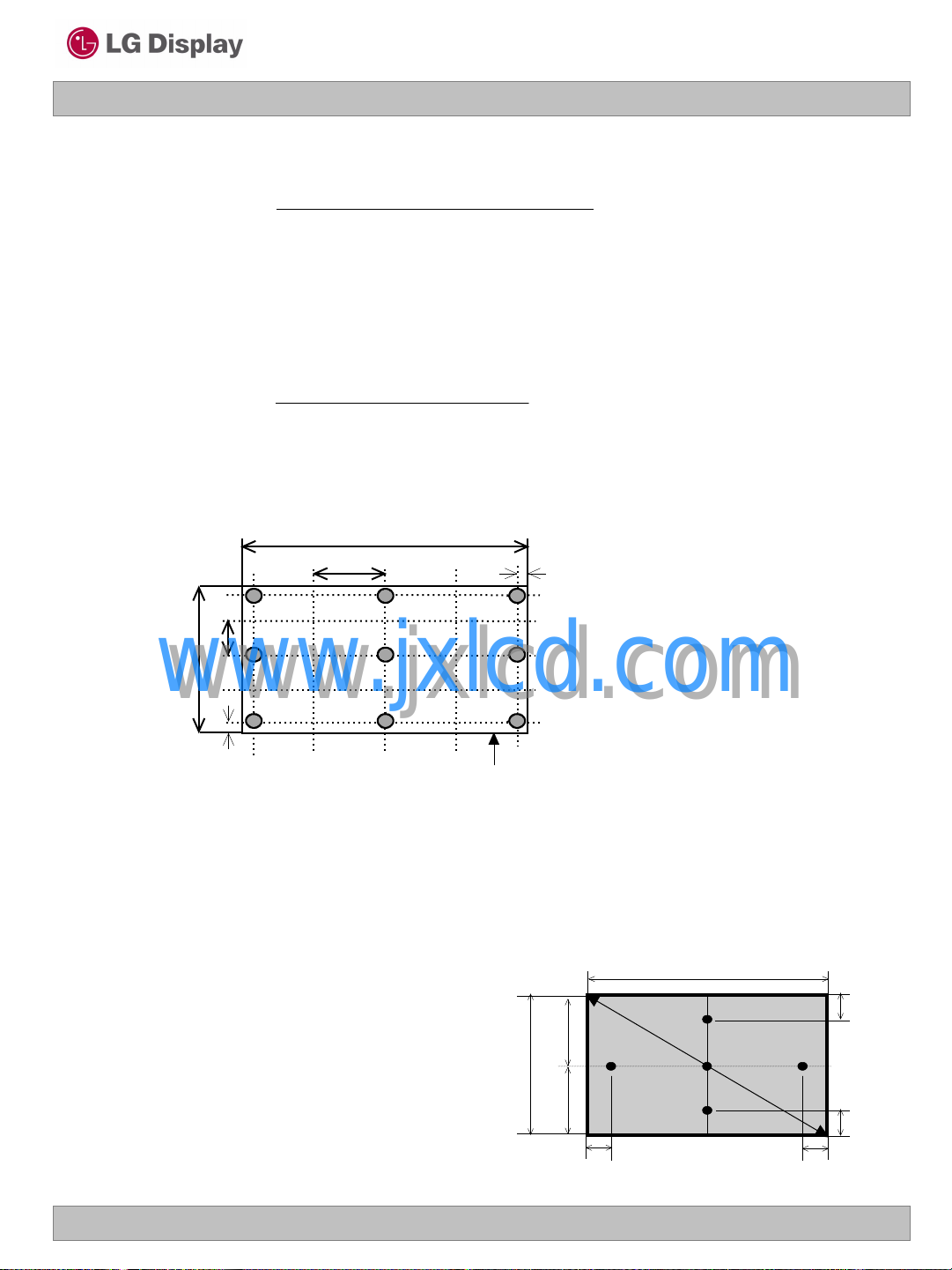
2. Surface luminance is luminance value at No.1 point across the LCD surface 50cm
from the surface with all pixels displaying white. For more information see FIG 2.
3. The variation in surface luminance , WHITE is defined as :
Measuring point for surface luminance & measuring point for luminance variation
H
A
H/10
LM201U05
2 3
B
V
www.jxlcd.com
www.jxlcd.com
V/10
A : H/4 mm
B : V/4 mm
@ H,V : Active Area
< Luminance Uniformity - angular – dependence (LR& TB)
TCO ‘03 Luminance uniformity – angular dependence, is the capacity of the VDU to present the same
luminance level independently of the viewing direction. The angular-dependent luminance uniformity is
calculated as the ratio of maximum luminance to minimum luminance in the specified measurement
areas.
Test pattern : 80% white pattern
Test point : 2-point
Test distance : D * 1.5 = 76.58㎝
Test method : LR = ((L
+ (L
TB = ((L
5
7 8
FIG. 2 Measure Point for Luminance
max.+30deg.
max. -30deg.
max.+15deg.
/ L
/ L
/ L
min. +30deg.
min. +15deg.
min. -30deg.
1
Active Area
)
)) / 2
)
4
6
9
H
D
T
V/2
V
V/2
L
C
B
R
V/10
V/10
FIG. 3 Measure Point for Luminance uniformity – angular dependence
Ver. 1.1 July. 17. 2008
H/10
H/10
21 / 34
LM201U05
Liquid Crystal Display
Product Specification
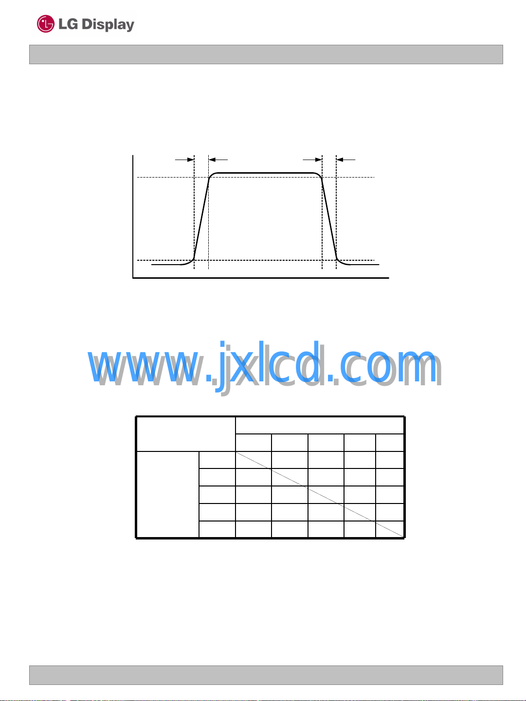
4. The response time is defined as the following figure and shall be measured by switching
the input signal for “black” and “white”.
Response time is the time required for the display to transition from black to white (Rise Time,
TrR) and from white to black (Decay Time, TrD).
TrR
100
90
Optical
Response
10
0
FIG. 4 Response Time
5. The Gray to Gray response time is defined as the following figure and shall be measured
by switching the input signal for “Gray To Gray “.
- Gray step : 5 Step
- T
- T
GTG_AVR
www.jxlcd.com
www.jxlcd.com
GTG_MAX
is the total average time at rising time and falling time for “Gray To Gray “.
is the max time at rising time or falling time for “Gray To Gray “.
Rising Time
Gray to Gray
TrD
G0G63G127G191G255
G255Falling Time
G191
G127
G63
G0
Ver. 1.1 July. 17. 2008
22 / 34
Product Specification
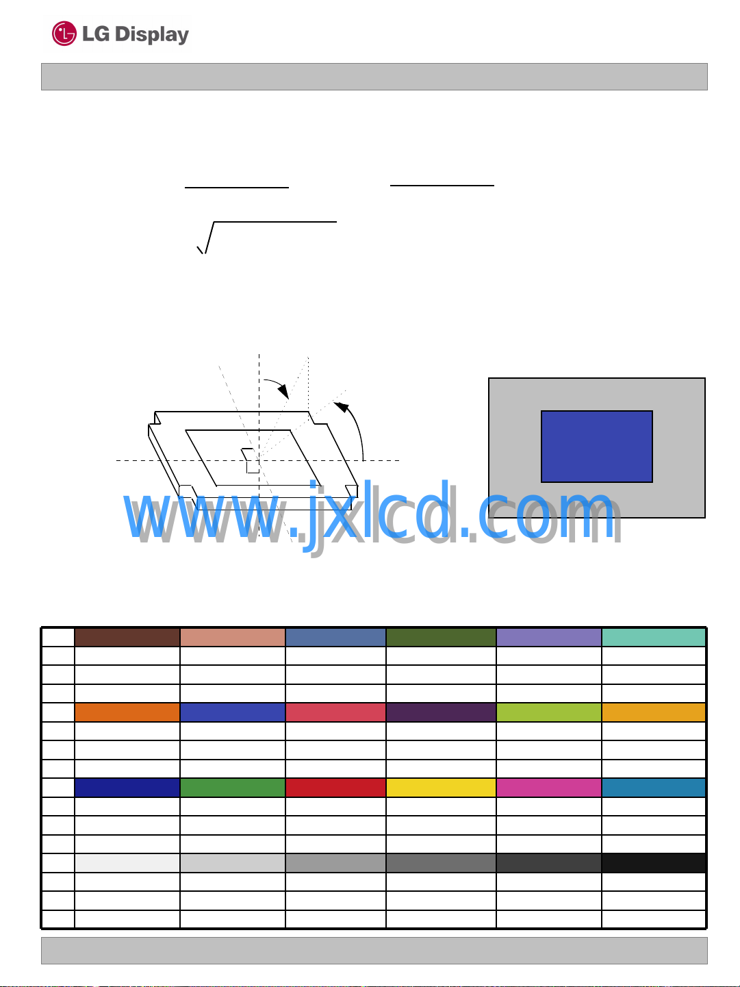
= 90。
(12:00)
yu
= 0。
z
z' yd
= 180。
(9:00)
A
= 0。
(3:00) xr
= 270。
(6:00)
TFT LCD
MODULE
xl
6. Color shift is the angle at which the color difference is lower than 0.04.
Color difference (Δu’v’)-
LM201U05
Liquid Crystal Display
u’=
Δu’v’ = (u’1-u’2)2+(v’1-v’2)
Pattern size : 25% Box size Viewing angle direction of color shift : Horizontal, Vertical -
www.jxlcd.com
www.jxlcd.com
4x
-2x + 12y + 3
v’=
2
u’1, v’1 : u’v’ value at viewing angle direction
u’2, v’2 : u’v’ value at front (θ=0)
9y
-2x + 12y +3
25% Box size
Viewing angle direction
Average RGB values in Bruce RGB for Macbeth Chart
Ver. 1.1 July. 17. 2008
Bluish greenBlue flowerFoliageBlue skyLight skinDark skin
114129778520698R
19911810211214256G
1781854616112345B
Orange yellowYellow greenPurpleModerate redPurplish blueOrange
2301607621156219R
162193396769104G
2958868717424B
cyanMagentaYellowRedGreenBlue
352072411977226R
126622122714832G
172151363765145B
blackNeutral 3.5Neutral 5Neutral 6.5Neutral 8White
2263110155206240R
2263110155206240G
2263110155206240B
23 / 34
Liquid Crystal Display
b
r
LaVL
)log()log()log( aVrLL
b
Product Specification
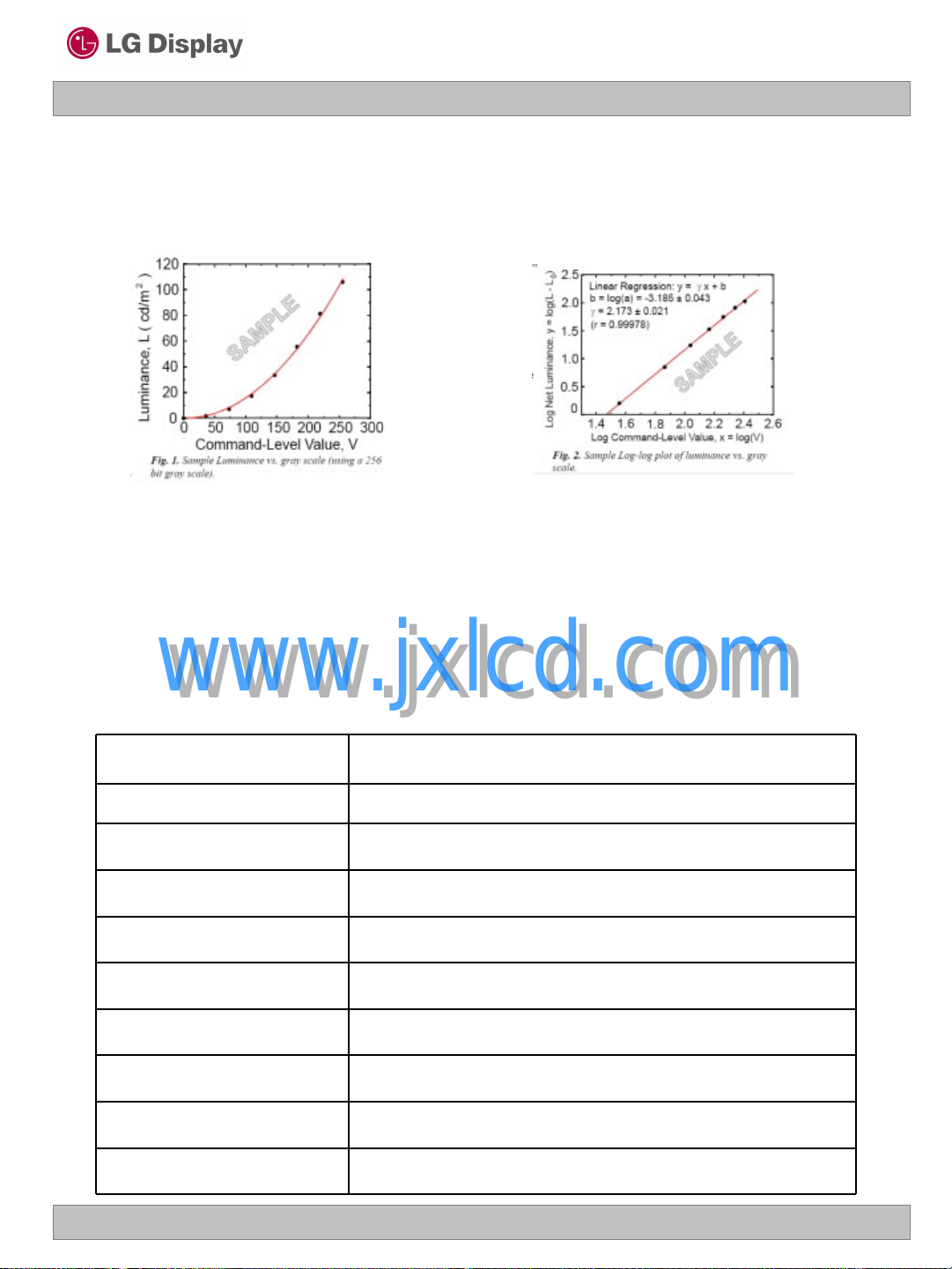
7. Viewing angle(general) is the angle at which the contrast ratio is greater than 10.
8. Effective viewing angle is the angle at which the gamma shift of gray scale is lower than 0.3.
FIG. 5
LM201U05
Here the Parameter α and γ relate the signal level V to the luminance L.
The GAMMA we calculate from the log-log representation (Fig. 4)
9. Gray scale specification
Gamma Value is approximately 2.2. For more information see Table 10.
Table 10. Gray Scale Specification
www.jxlcd.com
www.jxlcd.com
Relative Luminance [%] (Typ.)Gray Level
0.120
31
63
95
127
159
191
1.20
4.57
11.3
21.4
35.2
52.8
223
255
Ver. 1.1 July. 17. 2008
74.4
100
24 / 34
LM201U05
Liquid Crystal Display
Product Specification
5. Mechanical Characteristics
The contents provide general mechanical characteristics. In addition the figures in the next page are detailed
mechanical drawing of the LCD.
Horizontal
Outside dimensions
Bezel area
Active display area
Weight (approximate) 3,200g (Typ.) / 3250g (Max)
Surface Treatment
www.jxlcd.com
www.jxlcd.com
Notes : Please refer to a mechanic drawing in terms of tolerance at the next page.
Hard coating (3H)
Anti-glare treatment of the front polarizer Haze (25%)
Vertical
Depth
Horizontal
Vertical
Horizontal
Vertical
432.0 +0.4/-0.3mm
331.5 ± 0.5mm
25.0 ± 0.5 mm
413.0 mm
311.0 mm
408.0 mm
306.0 mm
Ver. 1.1 July. 17. 2008
25 / 34

<FRONT VIEW>
LM201U05
Liquid Crystal Display
Product Specification
www.jxlcd.com
www.jxlcd.com
Ver. 1.1 July. 17. 2008
26 / 34

<REAR VIEW>
LM201U05
Liquid Crystal Display
Product Specification
www.jxlcd.com
www.jxlcd.com
Ver. 1.1 July. 17. 2008
27 / 34

Product Specification
6. Reliability
Environment test condition
No Test Item Condition
LM201U05
Liquid Crystal Display
1
2
3
4
5
6
7
Vibration test
(non-operating)
www.jxlcd.com
www.jxlcd.com
Shock test
(non-operating)
Altitude
operating
storage / shipment
Ta= 60°C 240hHigh temperature storage test
Ta= -20°C 240hLow temperature storage test
Ta= 50°C 50%RH 240hHigh temperature operation test
Ta= 0°C 240hLow temperature operation test
(NDS conditions)
Wave form : random
Vibration level : 1.43G RMS
Bandwidth : 5-200Hz
Duration : X,Y,Z, 33 min
One time each direction
(LPL conditions)
Wave form : random
Vibration level : 1.0G RMS
Bandwidth : 10-500Hz
Duration : X,Y,Z, 20 min
One time each direction
Shock level : 120G
Waveform : half sine wave, 2ms
Direction : ±X, ±Y, ±Z
One time each direction
0 - 10,000 feet(3048m)
0 - 40,000 feet(12,192m)
Ver. 1.1 July. 17. 2008
28 / 34

Liquid Crystal Display
Product Specification
7. International Standards
7-1. Safety
a) UL 60950-1:2003, First Edition, Underwriters Laboratories, Inc.,
Standard for Safety of Information Technology Equipment.
b) CAN/CSA C22.2, No. 60950-1-03 1st Ed. April 1, 2003, Canadian Standards Association,
Standard for Safety of Information Technology Equipment.
c) EN 60950-1:2001, First Edition,
European Committee for Electrotechnical Standardization(CENELEC)
European Standard for Safety of Information Technology Equipment.
7-2. EMC
a) ANSI C63.4 “Methods of Measurement of Radio-Noise Emissions from Low-Voltage
Electrical and
Electrical Equipment in the Range of 9kHZ to 40GHz. “American National Standards
Institute(ANSI),
1992
b) C.I.S.P.R “Limits and Methods of Measurement of Radio Interface Characteristics of
Information
Technology Equipment.“ International Special Committee on Radio Interference.
Technology Equipment.“ European Committee for Electrotechnical
Standardization.(CENELEC), 1998
( Including A1: 2000 )
www.jxlcd.com
c) EN 55022 “Limits and Methods of Measurement of Radio Interface Characteristics of
www.jxlcd.com
Information
LM201U05
7-3. Environment
a) RoHS, Directive 2002/95/EC of the European Parliament and of the Council on the
reduction of
the use of certain hazardous substances in electrical and electronic equipment, January 2003.
Ver. 1.1 July. 17. 2008
29 / 34

Product Specification
8. Packing
8-1. Designation of Lot Mark
a) Lot Mark
A B C D E F G H I J K L M
A,B,C : SIZE(INCH) D : YEAR
E : MONTH F ~ M : SERIAL NO.
Note
1. YEAR
LM201U05
Liquid Crystal Display
Year
Mark
2. MONTH
Month
Mark
www.jxlcd.com
www.jxlcd.com
b) Location of Lot Mark
Serial No. is printed on the label. The label is attached to the backside of the LCD module.
This is subject to change without prior notice.
200320022001
321
200452005
4
Apr5May
4
2006720078200892009
6
Jun7Jul8Aug9Sep
6
2010
0
Oct
A
Nov
B
DecMarFebJan
C321
Ver. 1.1 July. 17. 2008
30 / 34

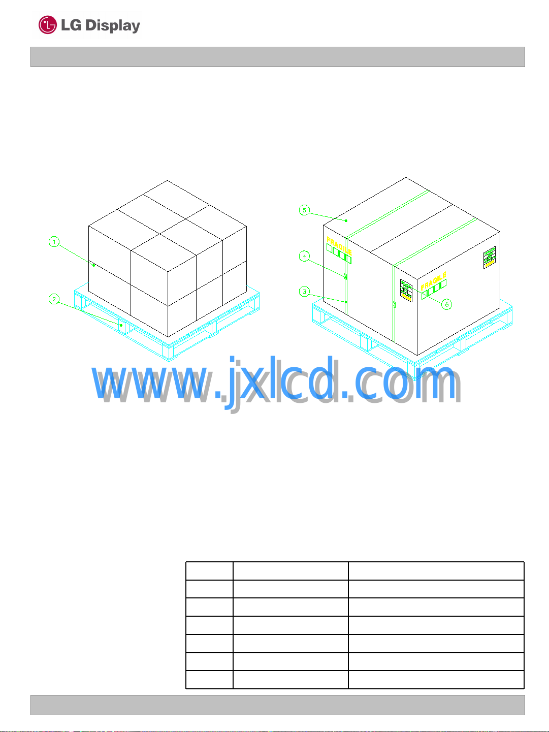
8-2. Packing Form
a) Package quantity in one box : 6EA
b) Box Size : 525 X 314 X 410
LM201U05
Liquid Crystal Display
Product Specification
www.jxlcd.com
www.jxlcd.com
DESCRIPTIONNO.
LCM1
MATERIAL
60G, A TYPESILICAGEL2
ALBAG3
OPPTAPE4
EPSPACKING, BOTTOM5
EPSPACKING, TOP6
PAPER, SWBOX7
OPPTAPE8
ARTLABEL9
Ver. 1.1 July. 17. 2008
31 / 34
8-3. Pallet Form
LM201U05
Liquid Crystal Display
Product Specification
www.jxlcd.com
www.jxlcd.com
DESCRIPTIONNO.
PACKING ASS’Y1
PLYWOOD_1080X980X117.5PALLET2
MATERIAL
PPBAND3
CLIPBAND, CLIP4
PAPER, SWANGLE PACKING5
ARTLABEL6
Ver. 1.1 July. 17. 2008
32 / 34
LM201U05
Liquid Crystal Display
Product Specification
9. PRECAUTIONS
Please pay attention to the followings when you use this TFT LCD module.
9-1. MOUNTING PRECAUTIONS
(1) You must mount a module using holes arranged in four corners or four sides.
(2) You should consider the mounting structure so that uneven force (ex. Twisted stress) is not applied to the
module. And the case on which a module is mounted should have sufficient strength so that
external
force is not transmitted directly to the module.
(3) Please attach the surface transparent protective plate to the surface in order to protect the polarizer.
Transparent protective plate should have sufficient strength in order to the resist external force.
(4) You should adopt radiation structure to satisfy the temperature specification.
(5) Acetic acid type and chlorine type materials for the cover case are not desirable because the former
generates corrosive gas of attacking the polarizer at high temperature and the latter causes
circuit break
by electro-chemical reaction.
(6) Do not touch, push or rub the exposed polarizers with glass, tweezers or anything harder than HB
pencil lead. And please do not rub with dust clothes with chemical treatment.
Do not touch the surface of polarizer for bare hand or greasy cloth.(Some cosmetics are detrimental
to the polarizer.)
(7) When the surface becomes dusty, please wipe gently with absorbent cotton or other soft materials like
chamois soaks with petroleum benzene. Normal-hexane is recommended for cleaning the
www.jxlcd.com
www.jxlcd.com
used to attach front / rear polarizers. Do not use acetone, toluene and alcohol because they
chemical damage to the polarizer.
(8) Wipe off saliva or water drops as soon as possible. Their long time contact with polarizer causes
deformations and color fading.
9-2. OPERATING PRECAUTIONS
(9) Do not open the case because inside circuits do not have sufficient strength.
adhesives
cause
(1) The spike noise causes the mis-operation of circuits. It should be lower than following voltage :
V=±200mV(Over and under shoot voltage)
(2) Response time depends on the temperature.(In lower temperature, it becomes longer.)
(3) Brightness depends on the temperature. (In lower temperature, it becomes lower.)
And in lower temperature, response time(required time that brightness is stable after turned on) becomes
longer.
(4) Be careful for condensation at sudden temperature change. Condensation makes damage to polarizer or
electrical contacted parts. And after fading condensation, smear or spot will occur.
(5) When fixed patterns are displayed for a long time, remnant image is likely to occur.
(6) Module has high frequency circuits. Sufficient suppression to the electromagnetic interference shall be
done by system manufacturers. Grounding and shielding methods may be important to minimized the
interference.
(7) Please do not give any mechanical and/or acoustical impact to LCM. Otherwise, LCM can not be
operated its full characteristics perfectly.
(8) A screw which is fastened up the steels should be a machine screw (if not, it causes metallic foreign
material and deal LCM a fatal blow)
(9) Please do not set LCD on its edge.
Ver. 1.1 July. 17. 2008
33 / 34

LM201U05
Liquid Crystal Display
Product Specification
9-3. ELECTROSTATIC DISCHARGE CONTROL
Since a module is composed of electronic circuits, it is not strong to electrostatic discharge. Make certain that
treatment persons are connected to ground through wrist band etc. And don’t touch interface pin directly.
9-4. PRECAUTIONS FOR STRONG LIGHT EXPOSURE
Strong light exposure causes degradation of polarizer and color filter.
9-5. STORAGE
When storing modules as spares for a long time, the following precautions are necessary.
(1) Store them in a dark place. Do not expose the module to sunlight or fluorescent light. Keep the
temperature between 5°C and 35°C at normal humidity.
(2) The polarizer surface should not come in contact with any other object.
It is recommended that they be stored in the container in which they were shipped.
9-6. HANDLING PRECAUTIONS FOR PROTECTION FILM
(1) The protection film is attached to the bezel with a small masking tape.
When the protection film is peeled off, static electricity is generated between the film and polarizer.
This should be peeled off slowly and carefully by people who are electrically grounded and with well
ion-blown equipment or in such a condition, etc.
(2) When the module with protection film attached is stored for a long time, sometimes there remains a
very small amount of glue still on the bezel after the protection film is peeled off.
(3) You can remove the glue easily. When the glue remains on the bezel surface or its vestige is
recognized, please wipe them off with absorbent cotton waste or other soft material like chamois
soaked with normal-hexane.
www.jxlcd.com
www.jxlcd.com
Ver. 1.1 July. 17. 2008
34 / 34
 Loading...