

LG LM-201U05-SLA1 Service manual
( ) Preliminary Specification
( ■ ) Final Specification
Title 20.1” UXGA TFT LCD
LM201U05
Liquid Crystal Display
Product Specification
SPECIFICATION
FOR
APPROVAL
BUYER General
MODEL
www.jxlcd.com
www.jxlcd.com
SIGNATURE DATE
/
/
/
SUPPLIER LG.Philips LCD CO., Ltd.
*MODEL LM201U05
SUFFIX SLA1
*When you obtain standard approval,
please use the above model name without suffix
Please return 1 copy for your confirmation with
your signature and comments.
Ver 1.0 Sep. 21 . 2005
1 /27
LM201U05
Liquid Crystal Display
Product Specification
CONTENTS
NO. ITEM Page
- COVER 1
- CONTENTS 2
- RECORD OF REVISIONS 3
1 GENERAL DESCRIPTION 4
2 ABSOLUTE MAXIMUM RATINGS 5
3 ELECTRICAL SPECIFICATIONS 6
3-1 ELECTRICAL CHARACTERISTICS 6
3-2 INTERFACE CONNECTIONS 8
3-3 SIGNAL TIMING SPECIFICATIONS 10
3-4 SIGNAL TIMING WAVE FORMS 11
3-5 COLOR INPUT DATA REFERENCE 12
3-6 POWER SEQUENCE 13
4 OPTICAL SPECIFICATIONS 14
5 MECHANICAL CHARACTERISTICS 19
www.jxlcd.com
6 RELIABILITY 22
7 INTERNATIONAL STANDARDS 23
7-1 SAFETY 23
7-2 EMC 23
8 PACKING 24
8-1 DESIGNATION OF LOT MARK 24
8-2 PACKING FORM 24
9 PRECAUTIONS 25
10 OTHERS -
www.jxlcd.com
APPENDIX 1. REQUIRED SIGNAL ASSIGNMENT FOR FLATLink Transmitter 27
Ver 1.0 Sep. 21 . 2005
2 /27
RECORD OF REVISIONS
Revision No DescriptionDate Page
LM201U05
Liquid Crystal Display
Product Specification
0.0
0.1
0.2
1.0
Jun. 23. 2005
Jul. 09. 2005
Jul. 25. 2005
Sep. 21. 2005
www.jxlcd.com
www.jxlcd.com
20,21,22
6
10
First Draft, Preliminary Specifications
Update Mechanical Dimension
Update The Electrical Specifications.
Change Timing Specifications.
Final Draft.
Ver 1.0 Sep. 21 . 2005
3 /27
LM201U05
Liquid Crystal Display
Product Specification
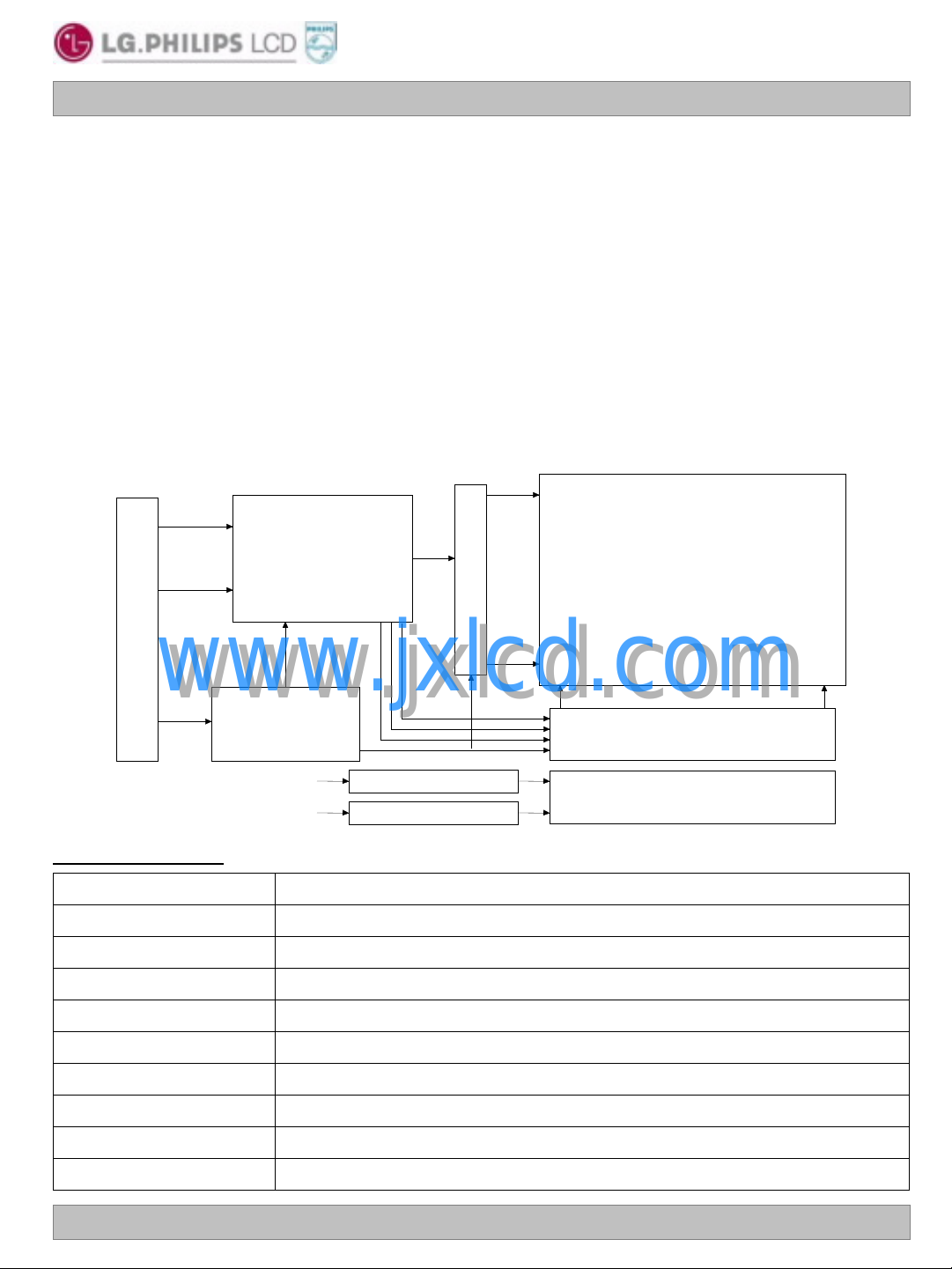
1. General Description
The LM201U05-SLA1 s a Color Active Matrix Liquid Crystal Display with an integral Cold Cathode Fluorescent
Lamp(CCFL) backlight system. The matrix employs a-Si Thin Film Transistor as the active element.
It is a transmissive type display operating in the normally black mode. This TFT-LCD has a 20.1 inch diagonally
measured active display area with UXGA resolution(1200 vertical by 1600 horizontal pixel array).
Each pixel is divided into Red, Green and Blue sub-pixels or dots which are arranged in vertical stripes.
Gray scale or the brightness of the sub-pixel color is determined with a 8-bit gray scale signal for each dot,
thus, presenting a palette of more than 16,777,216 colors.
The LM201U05-SLA1 has been designed to apply the interface method that enables low power, high speed,low
EMI. FPD Link must be used as a LVDS(Low Voltage Differential Signaling) chip.
The LM201U05-SLA1 is intended to support applications where thin thickness, wide viewing angle, low power are
critical factors and graphic displays are important. In combination with the vertical arrangement of the sub-pixels,
the LM201U05-SLA1 characteristics provide an excellent flat panel display for office automation products such as
monitors.
G1
Gate Driver Circuit
LVDS
CN1
(30pin)
pair #1
LVDS
pair #2
Timing Controller
&LVDS 1 Chip
TFT - LCD Panel
(1600 × RGB × 1200 pixels)
G1200
www.jxlcd.com
www.jxlcd.com
+18V
Vcc
Power Circuit
Block
CN1(4pin),CN2(2pin))
CN3(2pin),CN4(4pin)
RGB
S1 S1600
Source Driver Circuit
Back light Assembly (6CCFL)
General Features
Active screen size 20.1 inches (510.54mm) diagonal
Outline Dimension 432.0(H) x 331.5(V) x 25.0(D) mm(Typ.)
Pixel Pitch 0.255 mm x 0.255 mm
Pixel Format 1600 horizontal By 1200 vertical Pixels RGB stripe arrangement
Color depth 8-bits, 16,777,216 colors
Luminance, white 300 cd/m2(Typ. Center 1 point)
Power Consumption
Weight 3200g (Typ.)
Display operating mode Transmissive mode, normally black
Total 36.6 Watt(Typ.), ( 7.2 Watt @Vcc, 29.4 Watt @300cd/㎡ [Lamp=7.0mA])
Surface treatments Hard coating (3H), Anti-glare treatment of the front polarizer
Ver 1.0 Sep. 21 . 2005
4 /27
LM201U05
Liquid Crystal Display
Product Specification
2. Absolute Maximum Ratings
The following are maximum values which, if exceeded, may cause faulty operation or damage to the unit.
Table 1. ABSOLUTE MAXIMUM RATINGS
Parameter NotesSymbol
Power Input Voltage
Operating Temperature
Storage Temperature
Operating Ambient Humidity
Storage Humidity
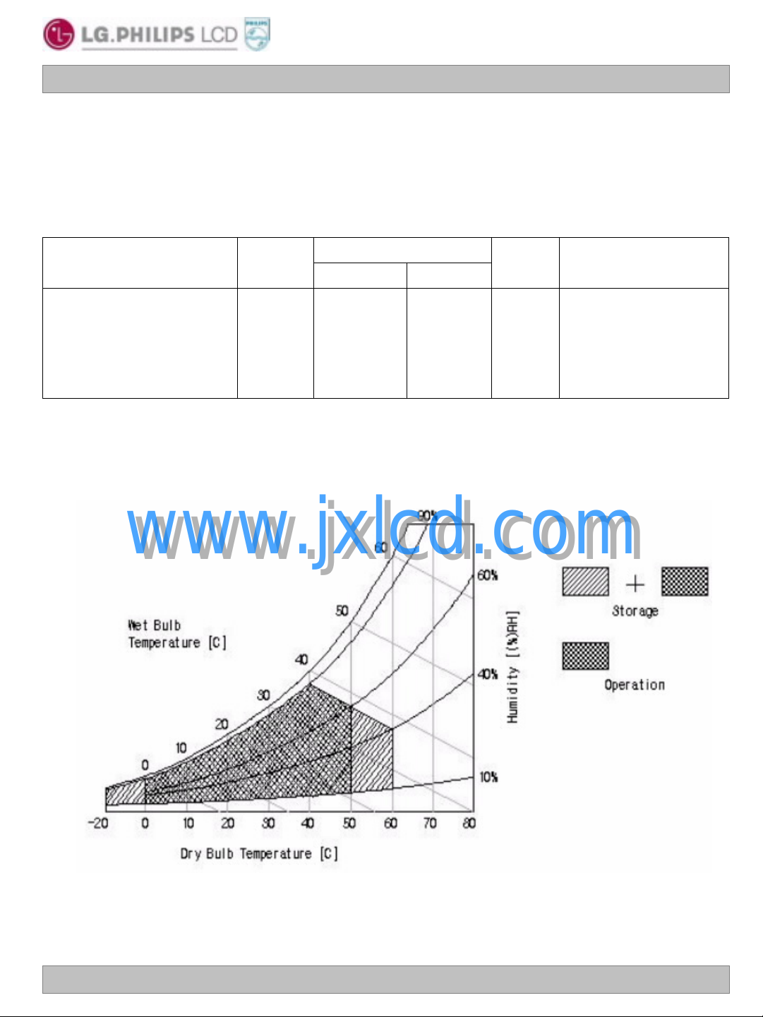
Note : 1. Temperature and relative humidity range are shown in the figure below.
Wet bulb temperature should be 39 °C Max, and no condensation of water.
www.jxlcd.com
www.jxlcd.com
V
CC
T
OP
T
ST
H
OP
H
ST
Values
Min. Max.
-0.3
0
-20
10
10
+23
+50
+60
+90
+90
Units
V
dc
℃
℃
%RH
%RH
at 25℃
1
1
1
1
Ver 1.0 Sep. 21 . 2005
5 /27
Liquid Crystal Display
Product Specification
3. Electrical Specifications
3-1. Electrical Characteristics
The LM201U05-SLA1requires two power inputs. One is employed to power the LCD electronics and to
drive the TFT array and liquid crystal. The second input which powers the CCFL, is typically generated
by an inverter. The inverter is an external unit to the LCD.
Table 2. ELECTRICAL CHARACTERISTICS
Values
Parameter
MODULE:
Power Supply Input Voltage
Power Supply Input Current
Power Consumption
Differential Impedance
Rush Current
LAMP (each CCFL)
Operating voltage
Operating Current
Established Starting Voltage
at 25℃
at 0℃
Operating Frequency
Power Consumption (6 CCFL’s)
Discharge Stabilization Time
Life time
www.jxlcd.com
www.jxlcd.com
Symbol
V
CC
I
CC
Pc
Zm
I
Rush
V
BL
I
BL
Vs
F
BL
P
BL
Ts
Min.
17V
670(8.0mA)
3.0
-
-
40
-
-
45000
Typ. Max.
18V
0.40
7.2
100
700
7.0
-
-
50
29.4
-
-
19V
0.60
10.8
3
825(3mA)
8.0
1150
1450
80
32.3
3
-
Vdc
A
W
Ohm
A
V
RMS
mA
V
RMS
V
RMS
KHz
Watts
Minutes
Hours
LM201U05
NotesUnits
1
1
2
3
4
5
6
7
8
9
Notes :1. The specified current and power consumption are under the VCC=18.0V, 25°C, fV=60Hz condition,
Typical supply current is measured at the condition of 8 X 6 chess pattern (white & black)
and Max supply current is measured at the sub 1dot pattern.
2. This impedance value is for impedance matching between LVDS TX and
the mating connector of the LCD.
3. The duration of rush current is about 1ms.
4. Operating voltage is measured at 25°C. The variance of the voltage is ±10%.
5. The output voltage at the transformer in the inverter must be high considering to the loss of the
ballast capacitor in the inverter. The voltage above VS should be applied to the lamps for more
than 1 second for start-up. Otherwise, the lamps may not be turned on.
6. Lamp frequency may produce interface with horizontal synchronous frequency and as a result this
may cause beat on the display. Therefore lamp frequency shall be as away possible from the
horizontal synchronous frequency and from its harmonics in order to prevent interference.
7. The lamp power consumption shown above does not include loss of external inverter at 25°C.
The used lamp current is the lamp typical current.
8. Let’s define the brightness of the lamp after being lighted for 5 minutes as 100%.
TS is the time required for the brightness of the center of the lamp to be not less than 95%.
The used lamp current is the lamp typical current.
9. The life time is defined as the time at which brightness of lamp is 50% compare to that of initial
value at the typical lamp current on condition of continuous operating at 252C.
Ver 1.0 Sep. 21 . 2005
6 /27
LM201U05
Liquid Crystal Display
Product Specification
Note. Do not attach a conducting tape to connecting wire.
If the lamp wire attach to a conducting tape, TFT-LCD Module has a low luminance and the
inverter has abnormal action. Because leakage current is occurred between lamp wire and
conducting tape.
The design of the inverter must have specifications for the lamp in LCD Assembly.
The performance of the Lamp in LCM, for example life time or brightness, is extremely influenced by
the characteristics of the DC-AC inverter. So all the parameters of an inverter should be carefully
designed so as not to produce too much leakage current from high-voltage output of the inverter.
When you design or order the inverter, please make sure unwanted lighting caused by the mismatch
of the lamp and the inverter(no lighting, flicker, etc) never occurs. When you confirm it, the LCD –
Assembly should be operated in the same condition as installed in you instrument.
Requirements for a system inverter design, which is intended to have a better display performance, a
better power efficiency and a more reliable lamp.
It shall help increase the lamp lifetime and reduce its leakage current.
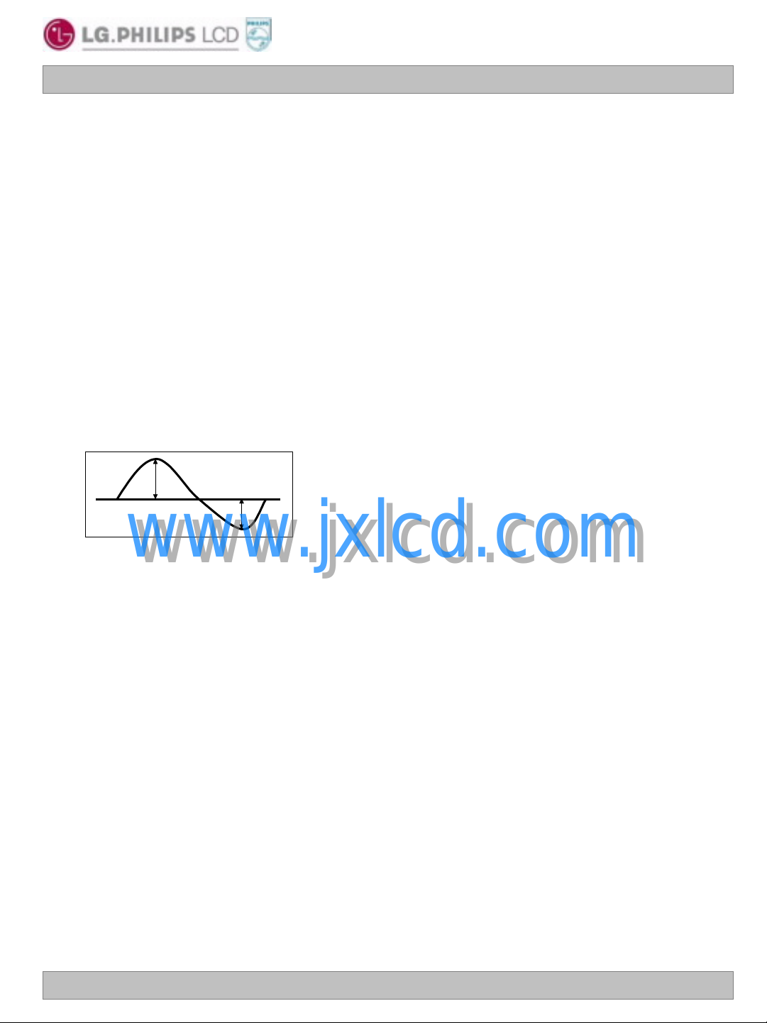
a. The asymmetry rate of the inverter current and voltage waveform should be 10% below;
b. The distortion rate of the current and voltage waveform should be within √2 ±10%;
c. The ideal sine current and voltage waveform shall be symmetric in positive and negative polarities.
* Asymmetry rate = | I p – I –p | / I
* Distortion rate = I p (or I –p) / I
I p
I -p
www.jxlcd.com
www.jxlcd.com
rms
rms
* 100%
Ver 1.0 Sep. 21 . 2005
7 /27
LM201U05
Liquid Crystal Display
Product Specification
3-2. Interface Connections
Interface chip must be used LVDS, part No. DS90CF383MTD(Transmitter) made by National Semiconductor.
Or used the compatible interface chips(TI:SN75LVDS83).
This LCD employs seven interface connections, a 30-pin connector is used for the module electronics interface.
Six 2-pin connectors are used for the integral back-light system.
The electronics interface connector is locking type and a model IS100-L30R-C23 manufactured by UJU or
FI-XB30SSRL-HF16 manufactured by JAE, The mating connector part number FI-X30M(JAE) or equivalent.
The pin configuration for the connector is shown in the table 3.
Table 3. MODULE CONNECTOR PIN CONFIGURATION(LVDS)
Pin DescriptionSymbol
1
2
3
4
5
6
7
8
9
10
11
12
13
14
15
16
17
18
19
20
21
22
23
24
25
26
27
28
29
30
Vcc
Vcc
Vcc
Vcc
NC
NC
SR3P
SR3M
SCLKINP
SCLKINM
SR2P
SR2M
SR1P
www.jxlcd.com
www.jxlcd.com
SR1M
SR0P
SR0M
GND
GND
FR3P
FR3M
FCLKINP
FCLKINM
FR2P
FR2M
FR1P
FR1M
FR0P
FR0M
GND
GND
Supply voltage for LCD module
Supply voltage for LCD module
Supply voltage for LCD module
Supply voltage for LCD module
NC (No Connection)
NC (No Connection)
Plus signal of even channel 3 (LVDS)
Minus signal of even channel 3 (LVDS)
Plus signal of even clock channel (LVDS)
Minus signal of even clock channel (LVDS)
Plus signal of even channel 2 (LVDS)
Minus signal of even channel 2 (LVDS)
Plus signal of even channel 1 (LVDS)
Minus signal of even channel 1 (LVDS)
Plus signal of even channel 0 (LVDS)
Minus signal of even channel 0 (LVDS)
Ground
Ground
Plus signal of odd channel 3 (LVDS)
Minus signal of odd channel 3 (LVDS)
Plus signal of odd clock channel (LVDS)
Minus signal of odd clock channel (LVDS)
Plus signal of odd channel 2 (LVDS)
Minus signal of odd channel 2 (LVDS)
Plus signal of odd channel 1 (LVDS)
Minus signal of odd channel 1 (LVDS)
Plus signal of odd channel 0 (LVDS)
Minus signal of odd channel 0 (LVDS)
Ground
Ground
Second data
First data
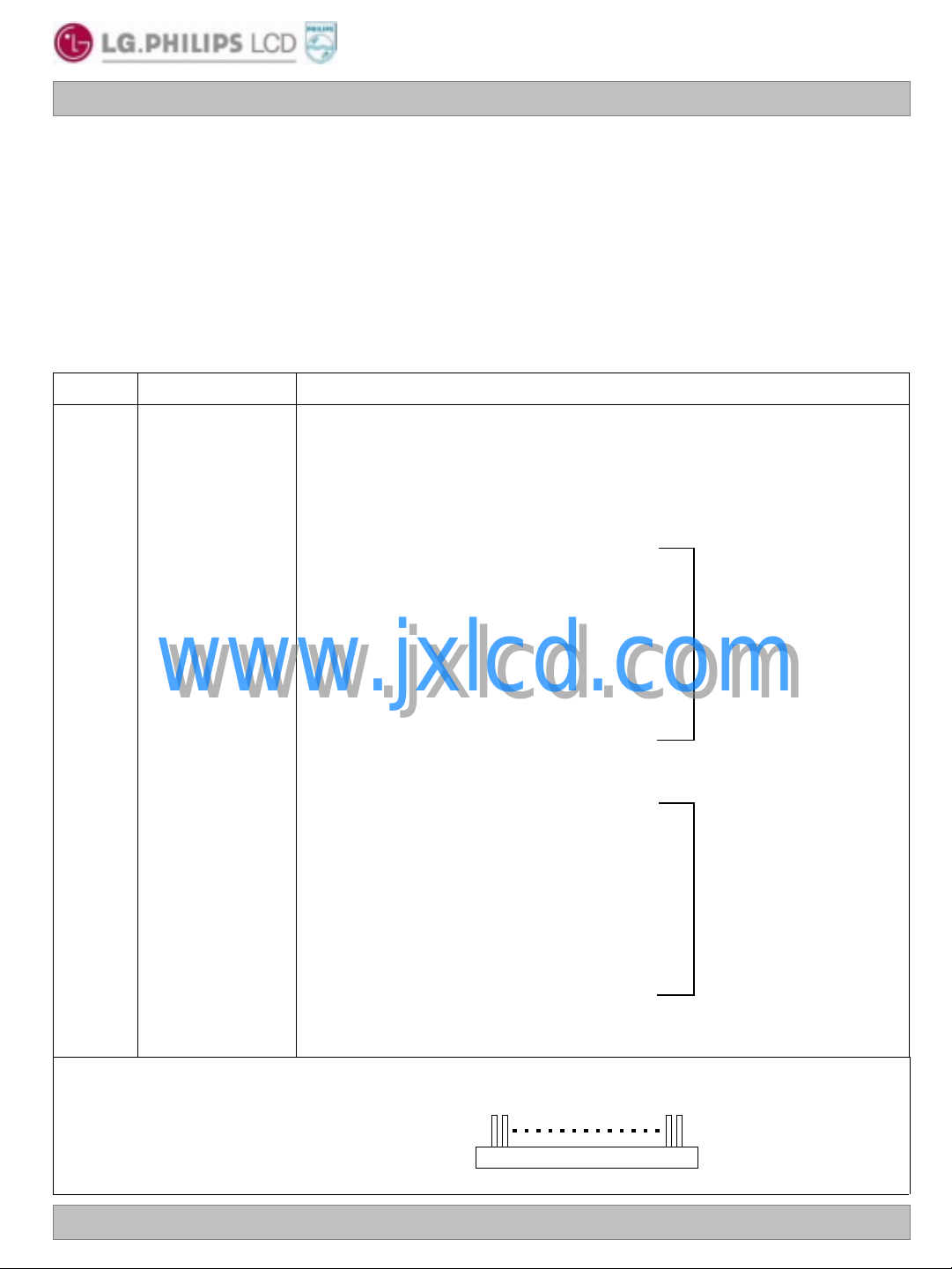
Connector pin arrangement
P/N, Maker :
IS100-L30R-C23 , UJU
Ver 1.0 Sep. 21 . 2005
130
8 /27
LM201U05
Liquid Crystal Display
Product Specification
The backlight interface connector is a model 1674817-1(CN2/CN3) manufactured by AMP ( or equivalent
BHSR-02VS-1 manufactured by JST) and BHR-05VS-1 (CN1/CN4) manufactured by JST. The mating
connector part number are SM02B-BHSS-1-TB(2pin), SM04(9-E2)B-BHS-1-TB or equivalent. The pin
configuration for the connector is shown in the table below.
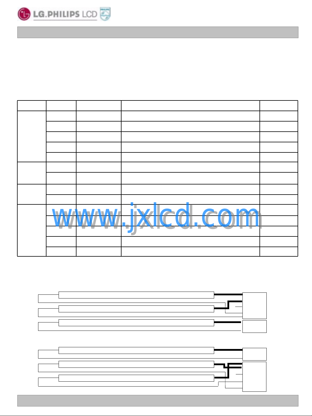
Table 4. BACKLIGHT CONNECTOR PIN CONFIGURATION
Symbol
CN1
5
CN2
CN3
CN4
www.jxlcd.com
www.jxlcd.com
5
Notes: 1. The high voltage power terminal is thick line.
2. The low voltage power terminal is thin line.
HV
HV
NC
LV
LV Power supply for lamp 2(Low voltage side)
HV
LV
HV 1Power supply for lamp 4(High voltage side)1
LV
HV
HV
NC
LV
LV Power supply for lamp 5Low voltage side)
NC3
Power supply for lamp 1(Low voltage side)4
Power supply for lamp 3(Low voltage side)2
Power supply for lamp 4(Low voltage side)2
NC3
Power supply for lamp 6(Low voltage side)4
NotesDescriptionPinNo
1Power supply for lamp 1(High voltage side)1
1Power supply for lamp 2(High voltage side)2
1Power supply for lamp 3(High voltage side)1
1Power supply for lamp 6(High voltage side)1
1Power supply for lamp 5(High voltage side)2
Ver 1.0 Sep. 21 . 2005
Up Side
Down Side
<BACKLIGHT CONNECTOR DIAGRAM>
Lamp1
Lamp 2
Lamp 3
Lamp 4
Lamp 5
Lamp 6
CN 1
CN 2
CN 3
CN 4
9 /27
 Loading...