

LG LM-201U02-A3C3 Service manual
( ) Preliminary Specification
( ● ) Final Specification
LM201U02
Liquid Crystal Display
Product Specification
SPECIFICATION
FOR
APPROVAL
20.1” UXGA TFT LCDTitle
BENQBUYER
MODEL
*When you obtain standard approval,
www.jxlcd.com
www.jxlcd.com
DATESIGNATURE
/
/
/
please use the above model name without suffix
S.W.Lee / G.Manager
REVIEWED BY
H. S. Baek / G. Manager
PREPARED BY
K.G Park / Manager
LG.Philips LCD Co., Ltd.SUPPLIER
LM201U02*MODEL
A3C3Suffix
DATESIGNATURE
Please return 1 copy for your confirmation with
your signature and comments.
The preliminary document is subject to change without prior notice.
Ver. 0.3 July.30. 2002
MNT/TV Products Engineering Dept.
LG. Philips LCD Co., Ltd
1/ 27
Product Specification
Contents
LM201U02
Liquid Crystal Display
PageITEMNo
COVER
CONTENTS
RECORD OF REVISIONS
GENERAL DESCRIPTION1
ABSOLUTE MAXIMUM RATINGS2
ELECTRICAL SPECIFICATIONS3
ELECTRICAL CHARACTREISTICS3-1
INTERFACE CONNECTIONS3-2
SIGNAL TIMING SPECIFICATIONS3-3
SIGNAL TIMING WAVEFORMS3-4
COLOR INPUT DATA REFERNECE3-5
www.jxlcd.com
www.jxlcd.com
POWER SEQUENCE3-6
OPTICAL SFECIFICATIONS4
MECHANICAL CHARACTERISTICS5
RELIABLITY6
1
2
3
4
5
6
6
8
11
12
13
14
15
19
22
INTERNATIONAL STANDARDS7
SAFETY7-1
EMC7-2
PACKING8
DESIGNATION OF LOT MARK8-1
PACKING FORM8-2
Ver. 0.3 July.30. 2002
23
23
23
24
24
24
25PRECAUTIONS9
27APPENDIX
2/ 27
Product Specification
RECORD OF REVISIONS
First Draft (Preliminary)-Nov.13.20010.0
LM201U02
Liquid Crystal Display
DESCRIPTIONPageRevision DateRevision No
4Feb.20.20020.1
4
19
19
15
www.jxlcd.com
www.jxlcd.com
Outline Dimension: 24.5(D) mm -> 24.3(D) mm
Weight: 4,100 g (typ.) ->3,700 g (typ.)
Outline Dimension: 24.1(D) mm(Max) -> 24.3(D) mm(Typ)
Weight: 4,100 g (Typ) ->3,700 g (Typ)
4,300 g (Max) ->4,000 g (Max)
Front View Update20
Rear View Update21
Electrical Characteristics Notes Update6,7
Front View Update20
Rear View Update21
4. Optical spec.
Response time changed
typ 30ms-Æ 25ms
Front View Update(Lamp Wire:165mm->175mm)20Mar.08.20020.2
Rear View Update21
TMDS signal interface connector 8Mar.21.2002
FI-WE21P-HF-E (JAE) ->FI-WE21P-HF-E (JAE)
GT121-21P-LD ( LG CABLE)
Added the table 815
Luminance Uniformity(TCO’99) : 1.7(max)
Front View Update20Mar.27.2002
Rear View Update21
CNC1 Pin Configuration:Pin 8-> No Connection8Apr.02.2002
CNC1 Pin Configuration:Pin 18-> No Connection8
CNC2 Pin Configuration:Pin 12-> No Connection9
Table 5; the color of backlight connector pin(LV) changed10Apr.17.2002
CN1: Pin2 (Blue -> Sky Blue), Pin 5(white -> Dark blue)
CN2: Pin 2(white -> black)
CN3: Pin 2(white -> black)
CN4: Pin2 (Blue -> Sky blue), Pin 5(white -> Dark blue)
Ver. 0.3 July.30. 2002
3/ 27
Product Specification
RECORD OF REVISIONS
LM201U02
Liquid Crystal Display
DESCRIPTIONPageRevision DateRevision No
16Jul.30.20020.3
www.jxlcd.com
www.jxlcd.com
4. Optical spec.
Viewing Angle changed
min 80 degreeÆ typ 88 degree
Ver. 0.3 July.30. 2002
4/ 27
LM201U02
Liquid Crystal Display
Product Specification
1. General Description
The LM201U02 LCD is a Color Active Matrix Liquid Crystal Display with an integral Cold Cathode Fluorescent
Lamp(CCFL) back light system. The matrix employs a-Si Thin Film Transistor as the active element. It is a
transmissive type display operating in the normally black mode. This TFT-LCD has a 20.1 inch diagonally
measured active display area with UXGA resolution(1200 vertical by 1600 horizontal pixel array). Each pixel is
divided into Red, Green and Blue sub-pixels or dots which are arranged in vertical stripes. Gray scale or the
luminance of the sub-pixel color is determined with a 8-bit gray scale signal for each dot, thus, presenting a
palette of more than 16,777,216 colors.
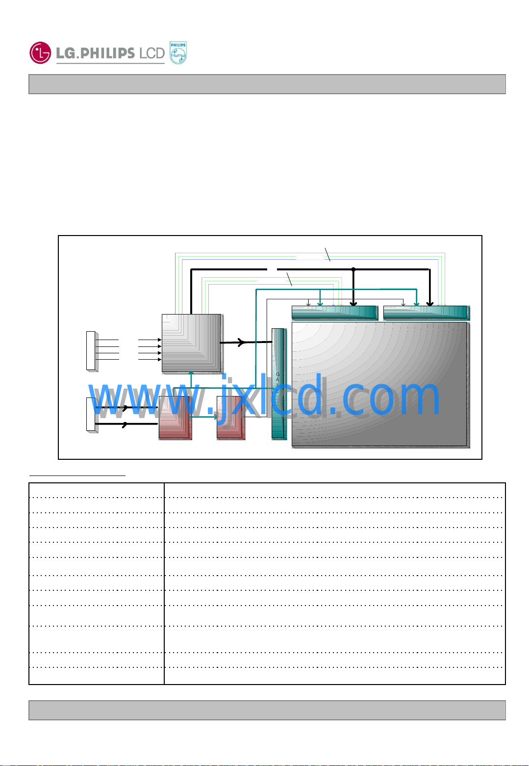
The LM201U02 has been designed to apply the TMDS
interface method to enables a simple and low-cost implementation in both the host and monitor.
VCC, VDD
TM
(Transition Minimized differential Signaling) as the
RGB (48BIT)
CLK
RGB (48BIT)
V0~V17
SOURCE (Right)SOURCE (Left)
(20PIN)
USER CON
INPUT 18V
www.jxlcd.com
www.jxlcd.com
(15PIN)
POWER CON
General Features
RXC +/RX0 +/RX1 +/RX2 +/-
GND
Timing
Controller
DC/DC
Converter
20.1 inches(51cm) diagonalActive Screen Size
467.8(H) x 361.0(V) x 24.3(D) mm(Typ.)Outline Dimension
0.255 mm x 0.255mmPixel Pitch
1600 horiz. By 1200 vert. Pixels RGB stripes arrangementPixel Format
8-bit, 16,777,216 colorsColor Depth
250 cd/m
Total 41.0 Watt(Typ.)Power Consumption
3,700 g (typ.)Weight
Transmissive mode, normally blackDisplay Operating Mode
2
GAMMA
(Typ.)Luminance, White
L
K
C
VCC,VGH,VGL
G
A
T
E
PANEL
1600 X 1200
Surface Treatment
Hard coating(3H)
Anti-glare treatment of the front polarizer,
TMDSInterface
6 CCFL’s(Cold Cathode Fluorescent Lamp)LAMP
Ver. 0.3 July.30. 2002
5/ 27

Liquid Crystal Display
Product Specification
2. Absolute Maximum Ratings
The following are maximum values which, if exceeded, may cause operation or damage to the unit.
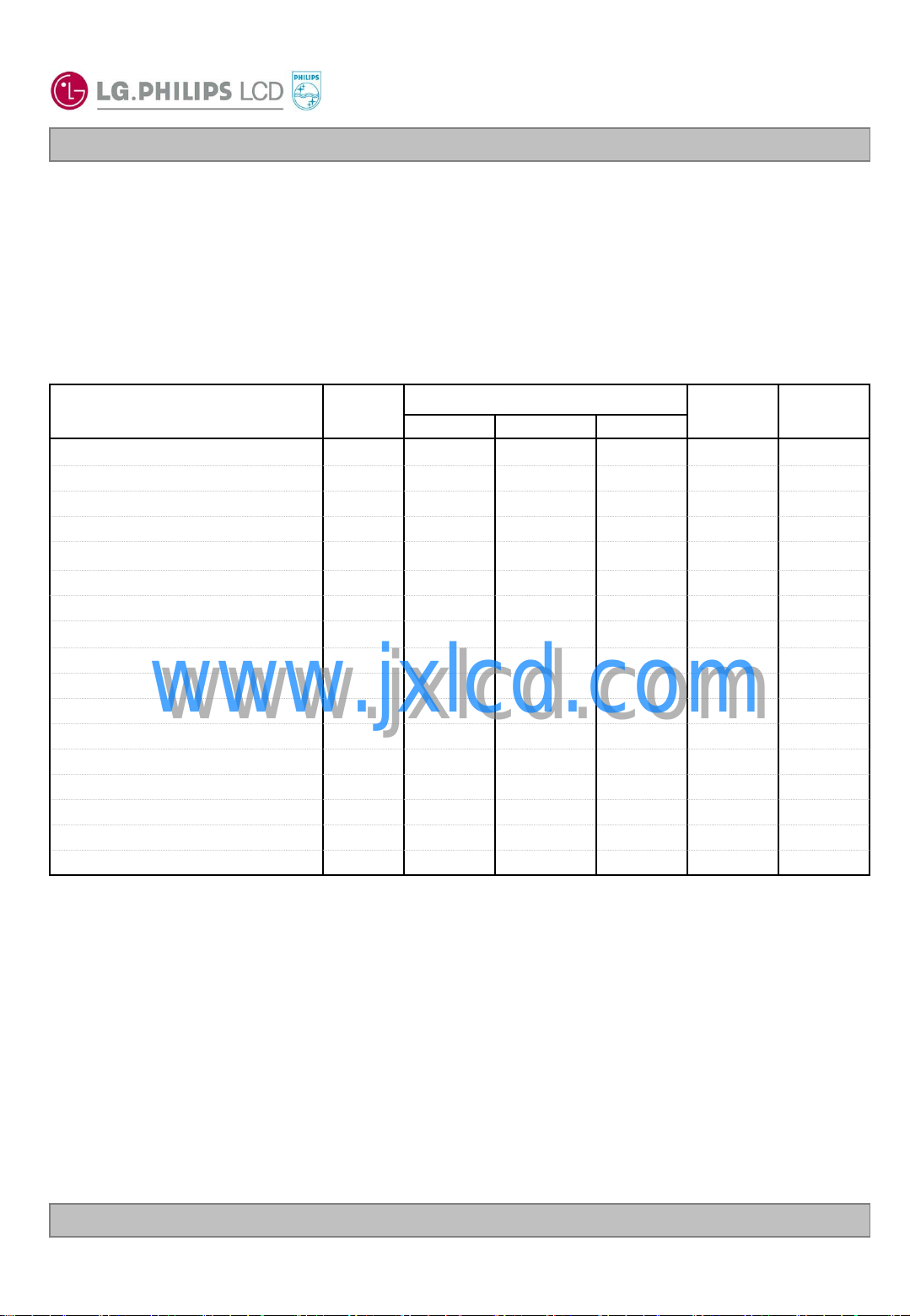
Table 1. ABSOLUTE MAXIMUM RATINGS
LM201U02
Parameter Notes
Power Input Voltage
Operating Temperature
Storage Temperature
Operating Ambient
Humidity
Storage Humidity
Note : 1. Temperature and relative humidity range are shown in the figure below.
Wet bulb temperature should be 39 °C Max, and no condensation of water.
www.jxlcd.com
www.jxlcd.com
Symbol
OP
ST
OP
ST
Values
MaxMin
500T
60-20H
Units
°C
°C
at 25 ± 5°CVdc21-0.3Vcc
1
1
1%RH9010H
1%RH9010H
Ver. 0.3 July.30. 2002
6/ 27
LM201U02
Liquid Crystal Display
Product Specification
3. Electrical Specifications
3-1. Electrical Characteristics
The LM201U02 requires two power inputs. One input is employed to power the LCD electronics and to
drive the voltages to drive the TFT array and liquid crystal. And the second input which powers the CCFL,
is typically generated by an inverter. The inverter is an external unit to the LCD.
Table 2. ELECTRICAL CHARACTERISTICS
Parameter Symbol
MODULE :
Inrush Current
LAMP :
Operating Voltage
Operating Current
www.jxlcd.com
www.jxlcd.com
at 25 °C
at 0 °C
Operating Frequency
Power Consumption
Rush
BL
BL
BL
BL
Values
MaxTypMin
Vdc22.020.018.0VccPower Supply Input Voltage
920(3mA)750(7.5mA)740(8mA)V
1080--
1500--
V
V
RMS
mA9.07.53.0I
RMS
RMS
NotesUnit
1A0.70.4-IccPower Supply Input Current
1Watt12.66.3-PcPower Consumption
2Ohm11010090ZmDifferential Impedance
3A3--I
3V
4VsEstablished Starting Voltage
5kHz605040F
6Watt37.233.8-P
7min3--TsDischarge Stabilization Time
8Hrs30,000Life Time
Notes : 1. The input current shall be measured at V
clock frequency of 125MHz under 256gray(B/W) (typ)
2. This impedance value is needed to proper display and measured from TMDS Tx output and
input connector of module.
3. The measuring condition
The duration of rush current is about 20ms, and rising time of Power input is 1ms.
4. Operating voltage is measured at 25°C. The variance of the voltage is ±10%.
5. The output voltage at the transformer in the inverter must be high considering to the loss of the
ballast capacitor in the inverter. The voltage above V
than 1 second for start-up. Otherwise, the lamps may not be turned on.
6. Lamp frequency may produce interface with horizontal synchronous frequency and as a result this
may cause beat on the display. Therefore lamp frequency shall be as away possible from the
horizontal synchronous frequency and from its harmonics in order to prevent interference.
Ver. 0.3 July.30. 2002
AA
of 18.0Vdc at 25℃, refresh rate of 60Hz, and pixel
should be applied to the lamps for more
S
7/ 27
LM201U02
Liquid Crystal Display
Product Specification
7. The lamp power consumption shown above does not include loss of external inverter at 25°C.
lamp current is the lamp typical current.
8. Let’s define the brightness of The used the lamp after being lighted for 5 minutes as 100%.
TS is the time required for the brightness of the center of the lamp to be not less than 95%.
The used lamp current is the lamp typical current.
9. The life time is defined as the time at which brightness of lamp is 50% compare to that of initial
value at the typical lamp current on condition of continuous operating at 25±2°C.
Note. Do not attach a conducting tape to connecting wire.
If the lamp wire attach to a conducting tape, TFT-LCD Module has a low luminance and the
inverter has abnormal action. Because leakage current is occurred between lamp wire and
conducting tape.
The design of the inverter must have specifications for the lamp in LCD Assembly.
The performance of the Lamp in LCM, for example life time or brightness, is extremely influenced by
the characteristics of the DC-AC inverter. So all the parameters of an inverter should be carefully
designed so as not to produce too much leakage current from high-voltage output of the inverter.
When you design or order the inverter, please make sure unwanted lighting caused by the mismatch
of the lamp and the inverter(no lighting, flicker, etc) never occurs. When you confirm it, the LCD –
Assembly should be operated in the same condition as installed in you instrument
Requirements for a system inverter design, which is intended to have a better display performance, a
better power efficiency and a more reliable lamp.
It shall help increase the lamp lifetime and reduce its leakage current.
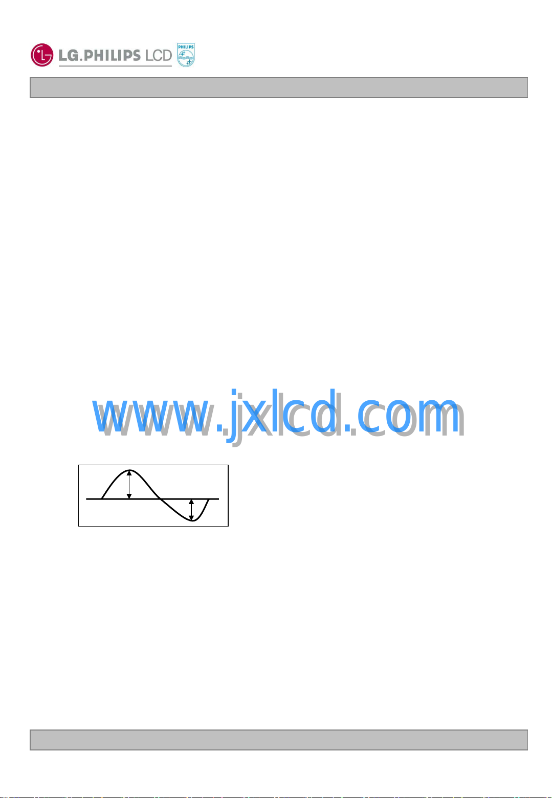
a. The asymmetry rate of the inverter current and voltage waveform should be 10% below;
b. The distortion rate of the current and voltage waveform should be within √2 ±10%;
c. The ideal sine current and voltage waveform shall be symmetric in positive and negative polarities.
www.jxlcd.com
www.jxlcd.com
* Asymmetry rate = | I
I
p
I
-p
Ver. 0.3 July.30. 2002
* Distortion rate = I
–I –p| / I
p
(or I –p) / I
p
rms
rms
* 100%
8/ 27
LM201U02
Liquid Crystal Display
Product Specification
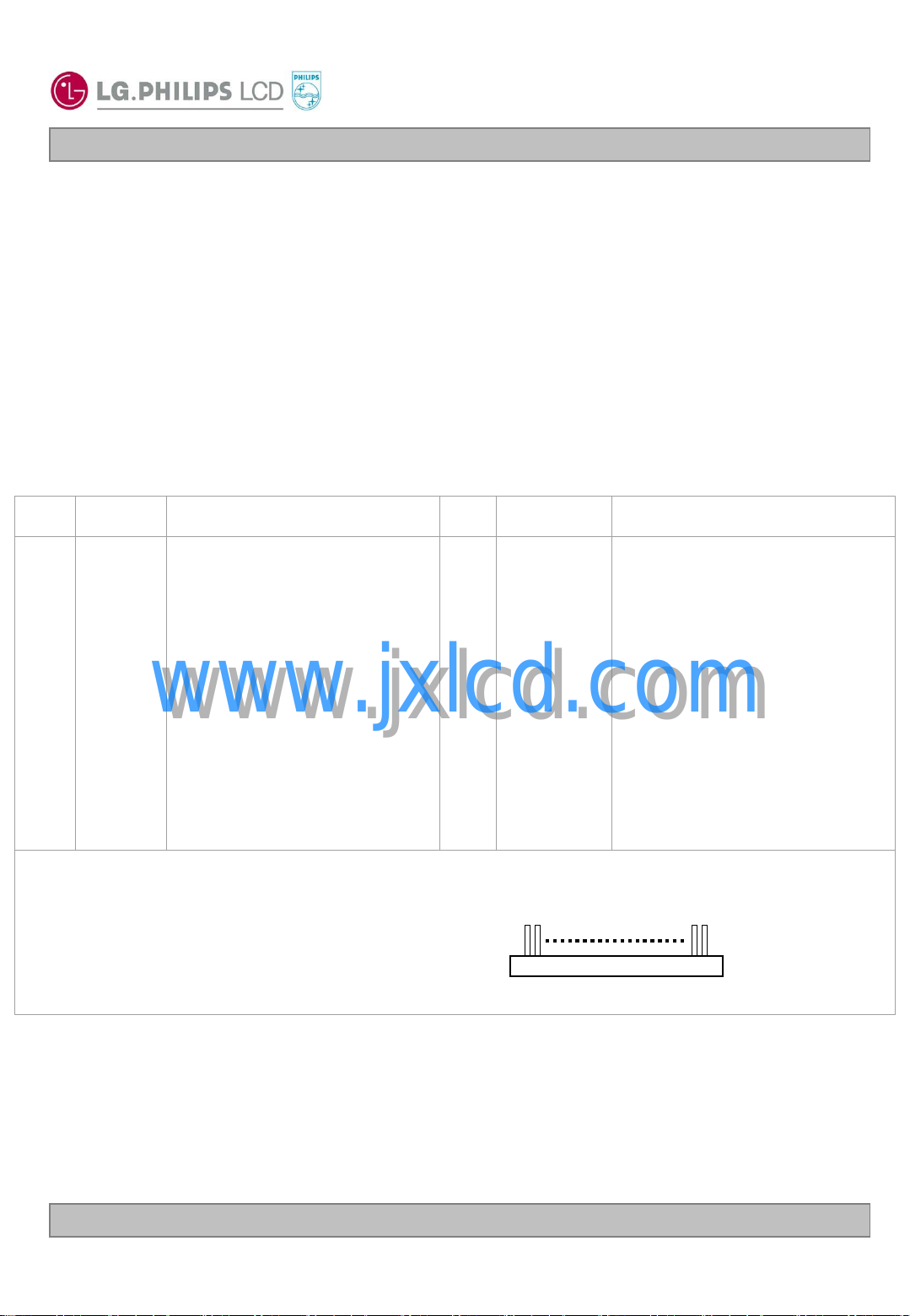
3-2. Interface Connections
This LCD employs three kinds of interface connections. A 21 pin connector is used for TMDS signals from
the host computer. A 15-pin connector is used for LCD module power and LCM controls signal from external
monitor control circuits. And four connectors, a three pin and two pin connector, are used for the integral
backlight system.
3-2-1. Signal Interface
The TMDS signal interface connector is FI-WE21P-HF-E by JAE and GT121-21P-LD by LG CABLE .
Interface chip in host side, must be used TMDS
equivalent.
The pin configuration for the 21 pin connector is shown in the table below.
Table 3 21PIN CONNECTOR (CNC1) PIN CONFIGURATION
TM
, part No. SiI160, designed by Silicon Image Inc., or its
Pin
10
1. Interface chips
2. Connector
Symbol Description Pin Symbol
1
TX1+
2
TX1-
3
SHLD1
4
SHLDC
5
TXC+
6
TXC-
7
GND
8
NC
9
NC
NC
1.1 LCD : Sil253(Silicon Image)
2.1 LCD : FI-WE21P-HF-E,GT121-21P-LD
2.2 Mating : FI-W21S or FI-W21M or compatible
2.3 Connector pin arrangement
TMDS positive differential output
(channel1)
TMDS negative differential output
(channel1)
Shield for TMDS channel 1
Shield for TMDS clock
TMDS positive differential output
(reference clock)
www.jxlcd.com
www.jxlcd.com
TMDS negative differential output
(reference clock)
Logic Ground
No Connection
No Connection
No Connection
11
12
13
14
15
16
17
18
19
20
21
TX2+
TX2-
SHLD2
SHLD0
TX0+
TX0-
NC
NC
DDC_DAT
DDC_CLK
NC
Description
TMDS positive differential output
(channel2)
TMDS negative differential output
(channel2)
Shield for TMDS channel 2
Shield for TMDS channel 0
TMDS positive differential output
(channel 0)
TMDS negative differential output
(channel 0)
No Connection
No Connection
DDC2B Data (See note 2)
DDC2B Clock (See note 3)
No connection
121
CNC1
Notes: 1. All shield pins and GND(ground) pin should be connected together and should also be
connected to the LCD’s metal frame.
2, 3. These pins are only for external monitor control circuits and directly connected to CNC2 connector.
Ver. 0.3 July.30. 2002
9/ 27
 Loading...