

LG LM-170E03-TLG4 Service manual
( ) Preliminary Specification
(◆) Final Specification
Title 17.0” SXGA TFT LCD
LM170E03
Liquid Crystal Display
Product Specification
SPECIFICATION
FOR
APPROVAL
BUYER
MODEL
www.jxlcd.com
www.jxlcd.com
SIGNATURE DATE
/
/
/
Philips
SUPPLIER LG Display Co., Ltd.
*MODEL LM170E03
SUFFIX TLG4
*When you obtain standard approval,
please use the above model name without suffix
APPROVED BY
G.T.KIM / G.Manager
REVIEWED BY
Y.W.LEE / Manager [C]
J.H.LEE / Manager [M]
D.Y.SEOK / Manager [P]
PREPARED BY
DATE
Please return 1 copy for your confirmation with
your signature and comments.
Ver 1.0 Mar. 05, 2008
D.G.KIM / Engineer
Product Engineering Dept.
LG Display Co., Ltd.
1 / 32
LM170E03
Liquid Crystal Display
Product Specification
CONTENTS
NO. ITEM Page
- COVER 1
- CONTENTS 2
- RECORD OF REVISIONS 3
1 GENERAL DESCRIPTION 4
2 ABSOLUTE MAXIMUM RATINGS 5
3 ELECTRICAL SPECIFICATIONS 6
3-1 ELECTRICAL CHARACTERISTICS 6
3-2 INTERFACE CONNECTIONS 9
3-3 SIGNAL TIMING SPECIFICATIONS 15
3-4 SIGNAL TIMING WAVEFORMS 16
3-5 COLOR INPUT DATA REFERANCE 17
3-6 POWER SEQUENCE 18
3-7 VCC POWER DIP CONDITION 19
4 OPTICAL SPECIFICATIONS 20
www.jxlcd.com
5 MECHANICAL CHARACTERISTICS 25
6 RELIABILITY 28
7 INTERNATIONAL STANDARDS 29
7-1 SAFETY 29
7-2 EMC 29
8 PACKING 30
8-1 DESIGNATION OF LOT MARK 30
8-2 PACKING FORM 30
9 PRECAUTIONS 31
www.jxlcd.com
Ver 1.0 Mar. 05, 2008
2 / 32

RECORD OF REVISIONS
Revision No DescriptionDate Page
LM170E03
Liquid Crystal Display
Product Specification
Ver 0.1
Ver 0.2
Ver 1.0
Nov. 30, 2007
Dec. 24, 2007
Mar. 05, 2008
www.jxlcd.com
www.jxlcd.com
4, 25
27
6
27
Preliminary Specifications
Update for Weight
-1890g(typ) 1600g(typ)
Update for Rear view
-Label change
Final Specifications
1) Update for Power input ripple
2) Update for Rear view
Ver 1.0 Mar. 05, 2008
3 / 32
LM170E03
Liquid Crystal Display
Product Specification
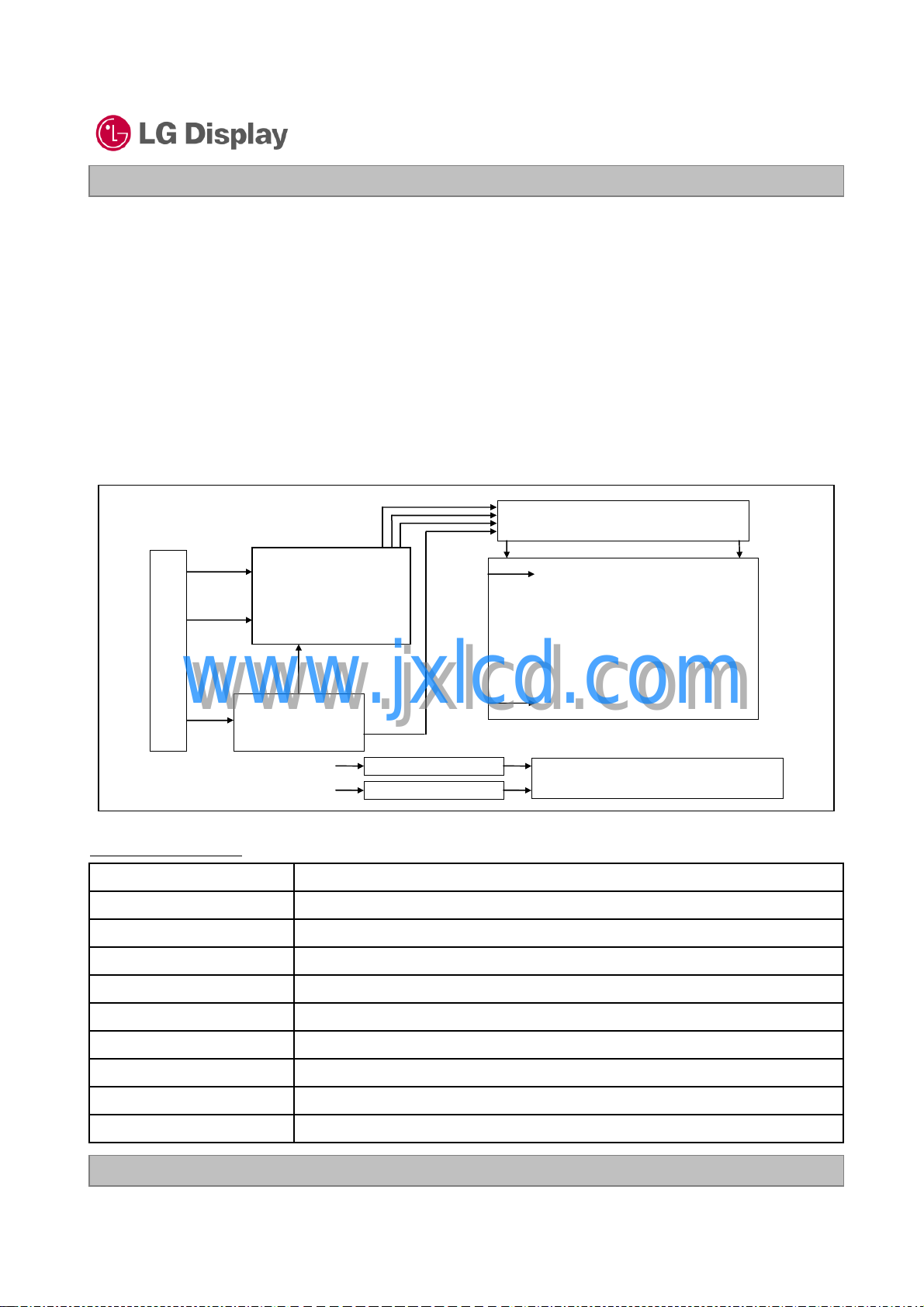
1. General Description
The LM170E03-TLG4 is a Color Active Matrix Liquid Crystal Display with an integral Cold Cathode Fluorescent
Lamp(CCFL) backlight system. The matrix employs a-Si Thin Film Transistor as the active element.
It is a transmissive type display operating in the normally white mode. This TFT-LCD has a 17.0 inch diagonal
measured active display area with SXGA resolution(1024 vertical by 1280 horizontal pixel array)
Each pixel is divided into Red, Green and Blue sub-pixels or dots which are arranged in vertical stripes.
Gray scale or the brightness of the sub-pixel color is determined with a 8-bit gray scale signal for each dot,
thus, presenting a palette of more than 16.7M colors with A-FRC(Advanced-Frame Rate Control).
The LM170E03-TLG4 has been designed to apply the interface method that enables low power, high speed,low
EMI. FPD Link or compatible must be used as a LVDS(Low Voltage Differential Signaling) chip.
The LM170E03-TLG4 is intended to support applications where thin thickness,wide viewing angle, low power are
critical factors and graphic displays are important. In combination with the vertical arrangement of the sub-pixels,
the LM170E03-TLG4 characteristics provide an excellent flat panel display for office automation products such as
monitors.
RGB
Source driver circuit
LVDS
pair #1
CN1
(30pin)
LVDS
pair #2
www.jxlcd.com
www.jxlcd.com
+5V
VLCD
Timing controller
&LVDS 1 chip
Power circuit
block
CN2, 3 (2pin)
CN4, 5 (2pin)
Figure 1. Block diagram
S1
G1
TFT - LCD Panel
(1280 × RGB × 1024 pixels)
G1024
Backlight assembly (4CCFL)
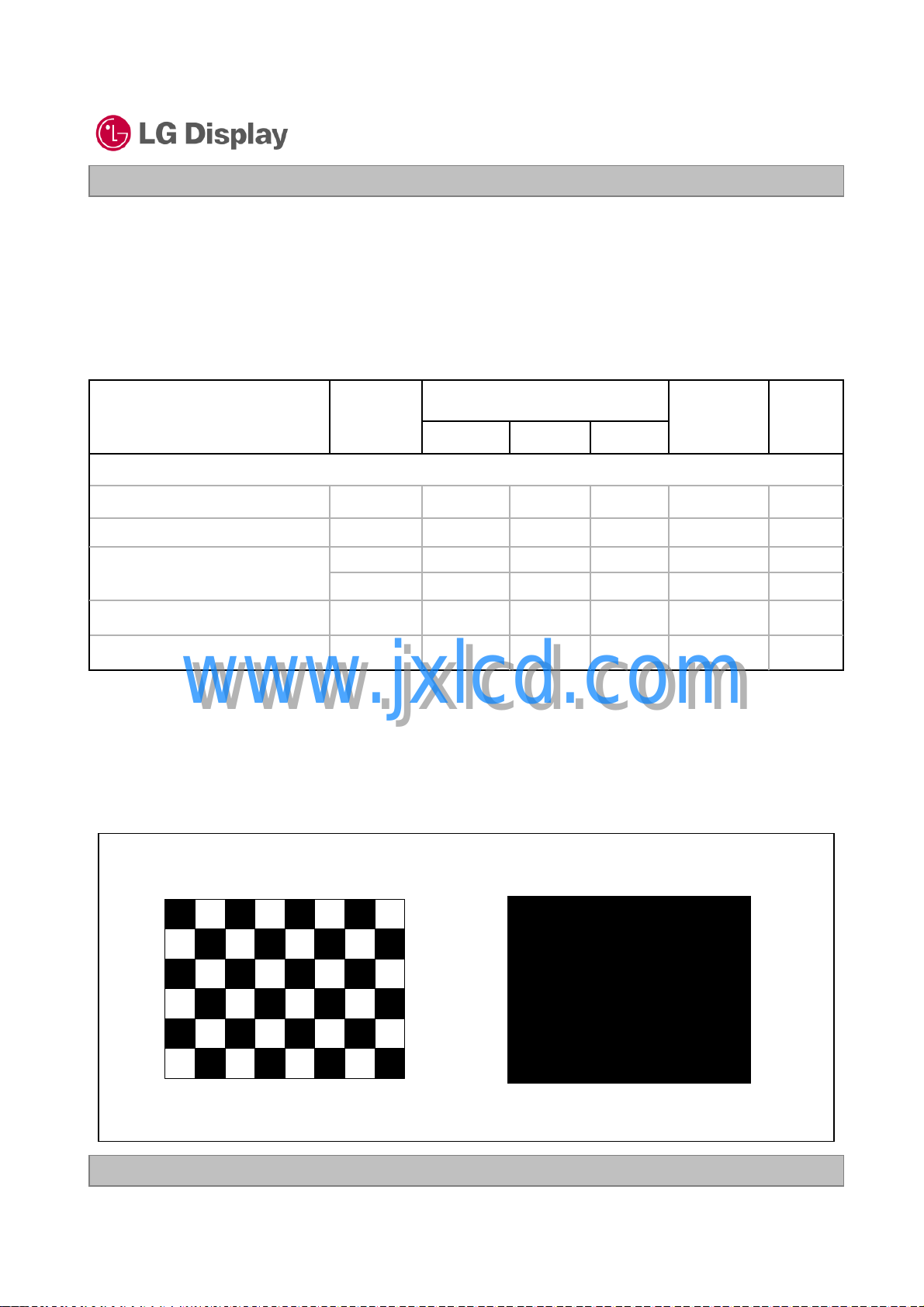
General Features
Active screen size 17.0 inch (43.27cm) diagonal
Outline Dimension 358.5(H) x 296.5(V) x 16.0(D) mm(Typ.)
Pixel Pitch 0.264 mm x 0.264 mm
Pixel Format 1280 horiz. by 1024 vert. Pixels. RGB stripe arrangement
Display Colors 16.7M colors
S1280
Luminance, white 300 cd/m2(Typ. Center 1 point)
Power Consumption 21.85 Watts(Typ.)
Weight 1600g (Typ.)
Display operating mode Transmissive mode, normally white
Surface treatments Hard coating (3H), Anti-glare treatment of the front polarizer
Ver 1.0 Mar. 05, 2008
4 / 32
LM170E03
Liquid Crystal Display
Product Specification
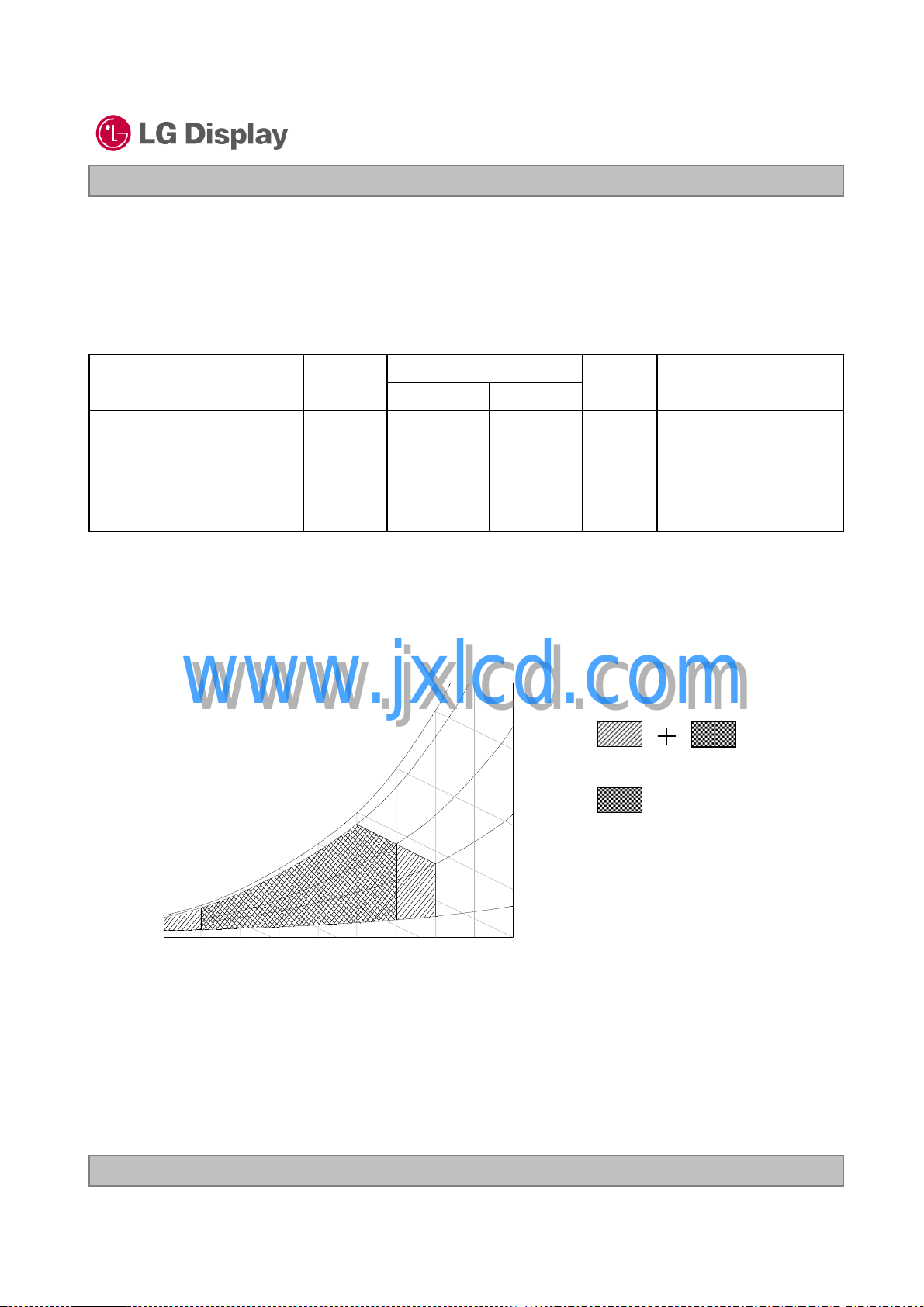
2. Absolute maximum ratings
The following are maximum values which, if exceeded, may cause faulty operation or damage to the unit.
Table 1. Absolute Maximum Ratings
Parameter NotesSymbol
Power Supply Input Voltage
Operating Temperature
Storage Temperature
Operating Ambient Humidity
Storage Humidity
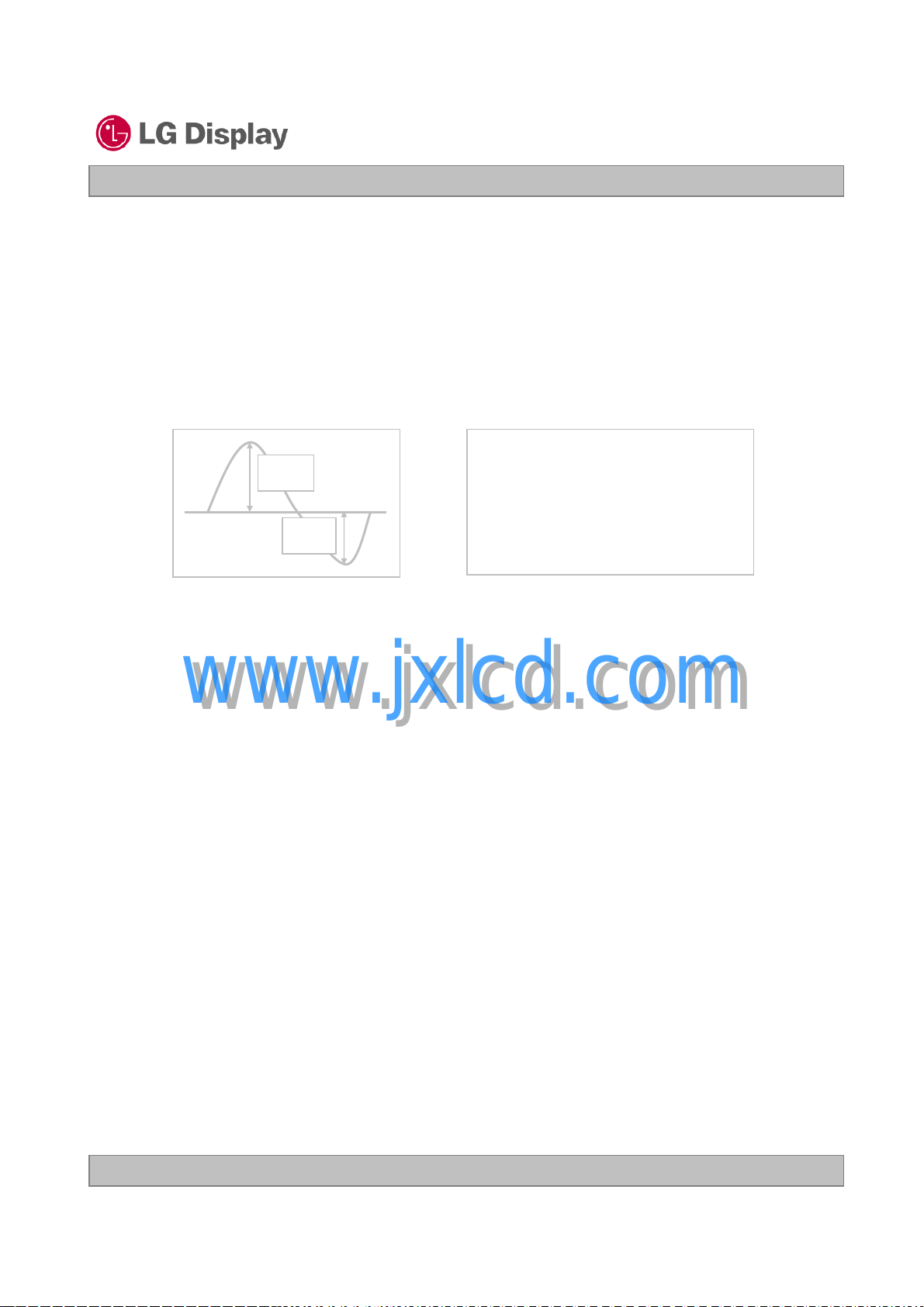
Note : 1. Temperature and relative humidity range are shown in the figure below.
Wet bulb temperature should be 39 °C Max, and no condensation of water.
www.jxlcd.com
www.jxlcd.com
Wet Bulb
Temperature [℃]
20
10
0
30
V
CC
T
OP
T
ST
H
OP
H
ST
50
40
Values
Min. Max.
-0.3
0
-20
10
10
90%
60
+5.5
+50
+60
+90
+90
60%
40%
10%
Units
V
dc
℃
℃
%RH
%RH
Operation
Humidity [(%)RH]
At 25℃
1
1
1
1
Storage
10 20 30 40 50 60 70 800-20
Dry Bulb Temperature [℃]
Figure 2. Temperature and relative humidity
Ver 1.0 Mar. 05, 2008
5 / 32
LM170E03
Liquid Crystal Display
Product Specification
3. Electrical specifications
3-1. Electrical characteristics
The LM170E03-TLG4 requires two power inputs. One is employed to power the LCD electronics and to
drive the TFT array and liquid crystal. Another which powers the CCFL, is typically generated by an inverter.
The inverter is an external unit to the LCD.
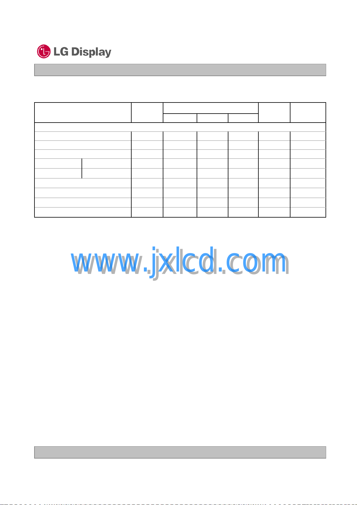
Table 2_1. ELECTRICAL CHARACTERISTICS
Values
Parameter Symbol
MaxTypMin
MODULE :
Vdc5.55.04.5VLCDPower Supply Input Voltage
Permissive Power Input Ripple 3V0.2--VLCD
NotesUnit
Power Supply Input Current
Note :
1. The specified current and power consumption are under the V
whereas mosaic pattern(8 x 6) is displayed and fVis the frame frequency.
2. The current is specified at the maximum current pattern.
3. Permissive power ripple should be measured under VCC=5.0V, 25°C, fV (frame frequency)=75Hz
condition and At that time, we recommend the bandwidth configuration of oscilloscope is to be under
20MHz.
4. The duration of rush current is about 2ms and rising time of power Input is 500us ± 20%.(min.).
www.jxlcd.com
www.jxlcd.com
White : 255Gray
Black : 0Gray
ILCD_BLACK
=5.0V, 25 ± 2°C,fV=60Hz condition
LCD
Maximum current pattern
1mA910790-ILCD_MOSAIC
2mA1090950-
1Watt4.553.95-PLCDPower Consumption
4A3--IRUSHRush current
Mosaic Pattern(8 x 6)
Ver 1.0 Mar. 05, 2008
Black Pattern
6 / 32
Product Specification
Table 2_2. ELECTRICAL CHARACTERISTICS
LM170E03
Liquid Crystal Display
Parameter Symbol
LAMP :
at 25 °C
at 0 °C
Operating Frequency
Discharge Stabilization Time
Power Consumption
Life Time
Note : The design of the inverter must have specifications for the lamp in LCD Assembly.
The performance of the Lamp in LCM, for example life time or brightness, is extremely influenced by
the characteristics of the DC-AC inverter. So all the parameters of an inverter should be carefully
designed so as not to produce too much leakage current from high-voltage output of the inverter.
When you design or order the inverter, please make sure unwanted lighting caused by the mismatch
www.jxlcd.com
of the lamp and the inverter (no lighting, flicker, etc) never occurs. When you confirm it, the LCD–
Assembly should be operated in the same condition as installed in you instrument.
※ Do not attach a conducting tape to lamp connecting wire.
If the lamp wire attach to a conducting tape, TFT-LCD Module has a low luminance and the inverter
has abnormal action. Because leakage current is occurred between lamp wire and conducting tape.
www.jxlcd.com
Values
MaxTypMin
745640628VBLOperating Voltage
7.57.02.5IBLOperating Current
1000
1250
RMS
RMS
V
RMS
V
RMS
NotesUnit
1, 2V
1mA
1, 3VsEstablished Starting Voltage
4kHz706040fBL
1, 5Min3Ts
6W19.7017.90PBL
1, 7Hrs50,000
1. Specified values are for a single lamp.
2. Operating voltage is measured at 25 ± 2°C. The variance of the voltage is ± 10%.
3. The voltage above VSshould be applied to the lamps for more than 1 second for start-up.
(Inverter open voltage must be more than lamp starting voltage.)
Otherwise, the lamps may not be turned on. The used lamp current is the lamp typical current.
4. Lamp frequency may produce interface with horizontal synchronous frequency and as a result this may
cause beat on the display. Therefore lamp frequency shall be as away possible from the horizontal
synchronous frequency and from its harmonics in order to prevent interference.
5. Let’s define the brightness of the lamp after being lighted for 5 minutes as 100%.
TSis the time required for the brightness of the center of the lamp to be not less than 95%.
6. The lamp power consumption shown above does not include loss of external inverter.
The used lamp current is the lamp typical current. (PBL= VBLx IBLx N
7. The life is determined as the time at which brightness of the lamp is 50% compared to that of initial
value at the typical lamp current on condition of continuous operating at 25 ± 2°C.
Ver 1.0 Mar. 05, 2008
Lamp
)
7 / 32
LM170E03
Liquid Crystal Display
Product Specification
8. The output of the inverter must have symmetrical(negative and positive) voltage waveform and
symmetrical current waveform (Unsymmetrical ratio is less than 10%). Please do not use the inverter
which has unsymmetrical voltage and unsymmetrical current and spike wave.
Requirements for a system inverter design, which is intended to have a better display performance, a
better power efficiency and a more reliable lamp, are following.
It shall help increase the lamp lifetime and reduce leakage current.
a. The asymmetry rate of the inverter waveform should be less than 10%.
b. The distortion rate of the waveform should be within √2 ±10%.
* Inverter output waveform had better be more similar to ideal sine wave.
* Asymmetry rate:
I p
| I p– I –p| / I
rms
x 100%
I -p
9. The inverter which is combined with this LCM, is highly recommended to connect coupling(ballast)
condenser at the high voltage output side. When you use the inverter which has not coupling(ballast)
condenser, it may cause abnormal lamp lighting because of biased mercury as time goes.
10.In case of edgy type back light with over 4 parallel lamps, input current and voltage wave form should
be synchronized
www.jxlcd.com
www.jxlcd.com
* Distortion rate
I p(or I –p) / I
rms
Ver 1.0 Mar. 05, 2008
8 / 32
LM170E03
Liquid Crystal Display
Product Specification
3-2. Interface Connections
Interface chip must be used LVDS, part No. SN75LVDS83 (Tx, Texas Instrument) or compatible.
This LCD employs a interface connection, a 30 pin connector is used for the module electronics interface.
Four 2pin connectors are used for the integral backlight system. The electronics interface connector is
a model IS100-L30B-C23 manufactured by UJU or 187024-30091 manufactured by P-TWO.
And mating connector is FI-X30H and FI-X30HL or it’s compatible manufactured by JAE.
The pin configuration for the connector is shown in the table 3 and the signal mapping with LVDS transmitter
is shown in the table 4.
Table 3. Module connector pin configuration
Pin No Symbol
1
2
3
4
5
6
7
8
9
10
11
12
13
14
15
16
17
18
19
20
21
22
23
24
25
26
27
28
29
30
RxO0RxO0+
RxO1RxO1+
RxO2RxO2+
GND
RxOCRxOC+
RxO3-
www.jxlcd.com
www.jxlcd.com
RxO3+
RxE0RxE0+
GND
RxE1RxE1+
GND
RxE2RxE2+
RxECRxEC+
RxE3RxE3+
GND
NC
NC
PWM_OUT
VCC
VCC
VCC
Description
LVDS Signal of Odd Channel 0(-)
LVDS Signal of Odd Channel 0(+)
LVDS Signal of Odd Channel 1(-)
LVDS Signal of Odd Channel 1(+)
LVDS Signal of Odd Channel 2(-)
LVDS Signal of Odd Channel 2(+)
Ground
LVDS Signal of Odd Channel Clock(-)
LVDS Signal of Odd Channel Clock(+)
LVDS Signal of Odd Channel 3(-)
LVDS Signal of Odd Channel 3(+)
LVDS Signal of Even Channel 0(-)
LVDS Signal of Even Channel 0(+)
Ground
LVDS Signal of Even Channel 1(-)
LVDS Signal of Even Channel 1(+)
Ground
LVDS Signal of Even Channel 2(-)
LVDS Signal of Even Channel 2(+)
LVDS Signal of Even Channel Clock(-)
LVDS Signal of Even Channel Clock(+)
LVDS Signal of Even Channel 3(-)
LVDS Signal of Even Channel 3(+)
Ground
No connection(For LCD internal use only)
No connection(For LCD internal use only)
PWM_OUT signal for control burst frequency of inverter
Power supply (5.0V Typ.)
Power supply (5.0V Typ.)
Power supply (5.0V Typ.)
First Pixel Data
Second Pixel Data
Ver 1.0 Mar. 05, 2008
9 / 32
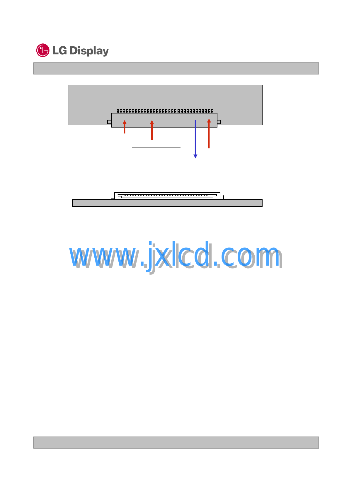
#1 #30
1’st signal pairs
2’nd signal pairs
#1 #30
LM170E03
Liquid Crystal Display
Product Specification
IS100-L30B-C23
Power(5V)
PWM signal
Rear view of LCM
[ Figure 4 ] Connector diagram
Notes: 1. All GND(ground) pins should be connected together and should also be
connected to the LCD’s metal frame.
www.jxlcd.com
www.jxlcd.com
2. All VCC(power input) pins should be connected together.
3. All NC pins should be separated from other signal or power.
4. PWM_OUT signal controls the burst frequency of a inverter.
This signal is synchronized with vertical frequency,
it’s frequency is 3 times of vertical frequency, and it’s duty ratio is 50%.
If you don’t use this pin, it is no connection.
Ver 1.0 Mar. 05, 2008
10 / 32
 Loading...