

Page 1

DVD/CD RECEIVER
SERVICE MANUAL
MODELS : LH-T360SE/LH-T3602SE/LH-T3600SE/LH-T361SE/LH-T360XSERVICE MANUAL
MODELS : LH-T360SE/LH-T3602SE/LH-T3600SE/
LH-T361SE/LH-T3630X
Page 2

1-1
[CONTENTS]
SECTION 1. GENERAL
• SERVICING PRECAUTIONS . . . . . . . . . . . . . . . . . . . . . . . . . . . . . . . . . . . . . . . . . . . . . . . 1-2
• ESD PRECAUTIONS . . . . . . . . . . . . . . . . . . . . . . . . . . . . . . . . . . . . . . . . . . . . . . . . . . . . 1-4
• SERVICE INFORMATION FOR EEPROM . . . . . . . . . . . . . . . . . . . . . . . . . . . . . . . . . . . . . 1-5
• SPECIFICATIONS . . . . . . . . . . . . . . . . . . . . . . . . . . . . . . . . . . . . . . . . . . . . . . . . . . . . . . . .1-6
SECTION 2. AUDIO PART
• AUDIO TROUBLESHOOTING GUIDE . . . . . . . . . . . . . . . . . . . . . . . . . . . . . . . . . . . . . . . . 2-1
• WIRING DIAGRAM . . . . . . . . . . . . . . . . . . . . . . . . . . . . . . . . . . . . . . . . . . . . . . . . . . . . . . . 2-4
• BLOCK DIAGRAM . . . . . . . . . . . . . . . . . . . . . . . . . . . . . . . . . . . . . . . . . . . . . . . . . . . . . . . 2-6
• CIRCUIT DIAGRAMS . . . . . . . . . . . . . . . . . . . . . . . . . . . . . . . . . . . . . . . . . . . . . . . . . . . . 2-8
• PRINTED CIRCUIT DIARGAMS . . . . . . . . . . . . . . . . . . . . . . . . . . . . . . . . . . . . . . . . . . . . 2-32
SECTION 3. DVD & AMP PART
• ELECTRICAL TROUBLESHOOTING GUIDE . . . . . . . . . . . . . . . . . . . . . . . . . . . . . . . . . . .3-1
• DVD & AMP CIRCUIT DIAGRAMS . . . . . . . . . . . . . . . . . . . . . . . . . . . . . . . . . . . . . . . . . .3-22
• PRINTED CIRCUIT DIARGAMS . . . . . . . . . . . . . . . . . . . . . . . . . . . . . . . . . . . . . . . . . . . . 3-30
SECTION 4. EXPLODED VIEWS . . . . . . . . . . . . . . . . . . . . . . . . . . . . . . . . . . . . .4-1
SECTION 5. SPEAKER PART . . . . . . . . . . . . . . . . . . . . . . . . . . . . . . . . . . . . . . .5-1
SECTION 6. REPLACEMENT PARTS LIST . . . . . . . . . . . . . . . . . . . . . . . . . . . . .6-1
Page 3
1-2
SERVICING PRECAUTIONS
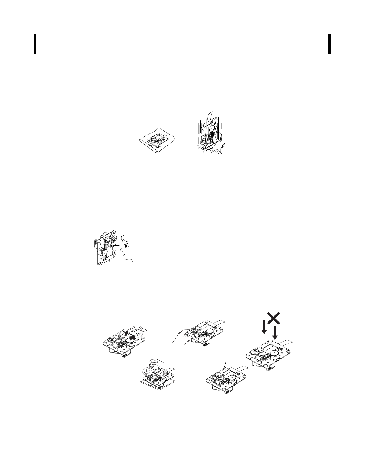
NOTES REGARDING HANDLING OF THE PICK-UP
1. Notes for transport and storage
1) The pick-up should always be left in its conductive bag until immediately prior to use.
2) The pick-up should never be subjected to external pressure or impact.
2. Repair notes
1) The pick-up incorporates a strong magnet, and so should never be brought close to magnetic materials.
2) The pick-up should always be handled correctly and carefully, taking care to avoid external pressure and
impact. If it is subjected to strong pressure or impact, the result may be an operational malfunction and/or
damage to the printed-circuit board.
3) Each and every pick-up is already individually adjusted to a high degree of precision, and for that reason
the adjustment point and installation screws should absolutely never be touched.
4) Laser beams may damage the eyes!
Absolutely never permit laser beams to enter the eyes!
Also NEVER switch ON the power to the laser output part (lens, etc.) of the pick-up if it is damaged.
5) Cleaning the lens surface
If there is dust on the lens surface, the dust should be cleaned away by using an air bush (such as used
for camera lens). The lens is held by a delicate spring. When cleaning the lens surface, therefore, a cotton swab should be used, taking care not to distort this.
6) Never attempt to disassemble the pick-up.
Spring by excess pressure. If the lens is extremely dirty, apply isopropyl alcohol to the cotton swab.
(Do not use any other liquid cleaners, because they will damage the lens.) Take care not to use too much
of this alcohol on the swab, and do not allow the alcohol to get inside the pick-up.
Storage in conductive bag
Drop impact
NEVER look directly at the laser beam, and don’t let
contact fingers or other exposed skin.
Magnet
How to hold the pick-up
Conductive Sheet
Cotton swab
Pressure
Pressure
SECTION 1. GENERAL
Page 4
1-3
NOTES REGARDING COMPACT DISC PLAYER REPAIRS
1. Preparations
1) Compact disc players incorporate a great many ICs as well as the pick-up (laser diode). These components
are sensitive to, and easily affected by, static electricity. If such static electricity is high voltage, components
can be damaged, and for that reason components should be handled with care.
2) The pick-up is composed of many optical components and other high-precision components. Care must be
taken, therefore, to avoid repair or storage where the temperature of humidity is high, where strong magnetism is present, or where there is excessive dust.
2. Notes for repair
1) Before replacing a component part, first disconnect the power supply lead wire from the unit
2) All equipment, measuring instruments and tools must be grounded.
3) The workbench should be covered with a conductive sheet and grounded.
When removing the laser pick-up from its conductive bag, do not place the pick-up on the bag. (This is
because there is the possibility of damage by static electricity.)
4) To prevent AC leakage, the metal part of the soldering iron should be grounded.
5) Workers should be grounded by an armband (1M Ω)
6) Care should be taken not to permit the laser pick-up to come in contact with clothing, in order to prevent
static electricity changes in the clothing to escape from the armband.
7) The laser beam from the pick-up should NEVER be directly facing the eyes or bare skin.
Resistor
(1 Mohm)
Conductive
Sheet
Resistor
(1 Mohm)
Armband
Page 5
1-4
ESD PRECAUTIONS
Electrostatically Sensitive Devices (ESD)
Some semiconductor (solid state) devices can be damaged easily by static electricity. Such components
commonly are called Electrostatically Sensitive Devices (ESD). Examples of typical ESD devices are integrated
circuits and some field-effect transistors and semiconductor chip components. The following techniques should
be used to help reduce the incidence of component damage caused by static electricity.
1. Immediately before handling any semiconductor component or semiconductor-equipped assembly, drain off
any electrostatic charge on your body by touching a known earth ground. Alternatively, obtain and wear a
commercially available discharging wrist strap device, which should be removed for potential shock reasons
prior to applying power to the unit under test.
2. After removing an electrical assembly equipped with ESD devices, place the assembly on a conductive surface
such as aluminum foil, to prevent electrostatic charge buildup or exposure of the assembly.
3. Use only a grounded-tip soldering iron to solder or unsolder ESD devices.
4. Use only an anti-static solder removal device. Some solder removal devices not classified as "anti-static" can
generate electrical charges sufficient to damage ESD devices.
5. Do not use freon-propelled chemicals. These can generate electrical charges sufficient to damage ESD
devices.
6. Do not remove a replacement ESD device from its protective package until immediately before you are
ready to install it. (Most replacement ESD devices are packaged with leads electrically shorted together by
conductive foam, aluminum foil or comparable conductive materials).
7. Immediately before removing the protective material from the leads of a replacement ESD device, touch the
protective material to the chassis or circuit assembly into which the device will by installed.
CAUTION : BE SURE NO POWER IS APPLIED TO THE CHASSIS OR CIRCUIT, AND OBSERVE ALL OTHER
SAFETY PRECAUTIONS.
8. Minimize bodily motions when handing unpackaged replacement ESD devices. (Otherwise harmless motion
such as the brushing together of your clothes fabric or the lifting of your foot from a carpeted floor can generate static electricity sufficient to damage an ESD device).
CAUTION. GRAPHIC SYMBOLS
THE LIGHTNING FLASH WITH APROWHEAD SYMBOL. WITHIN AN EQUILATERAL TRIANGLE, IS
INTENDED TO ALERT THE SERVICE PERSONNELTO THE PRESENCE OF UNINSULATED
“DANGEROUS VOLTAGE” THAT MAY BE OF SUFFICIENT MAGNITUDE TO CONSTITUTE A RISK OF
ELECTRIC SHOCK.
THE EXCLAMATION POINTWITHIN AN EQUILATERAL TRIANGLE IS INTENDED TO ALERT THE
SERVICE PERSONNEL TO THE PRESENCE OF IMPORTANT SAFETY INFORMATION IN SERVICE
LITERATURE.
Page 6
1-5
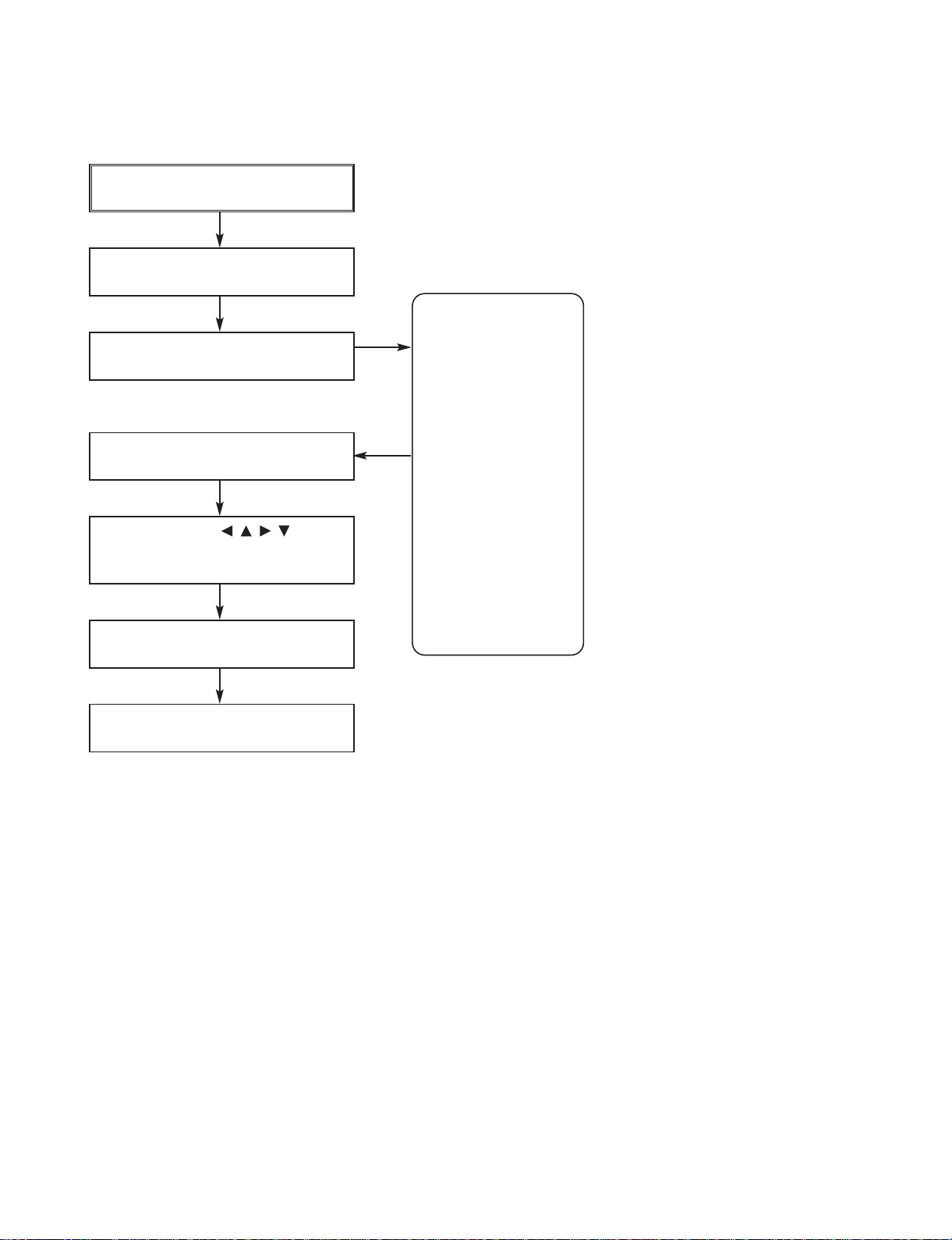
SERVICE INFORMATION FOR EEPROM
POWER ON
DVD LOGO Status (NO Disk status)
Remotecontrol
Pause key-->1-->4-->7-->2 in order.
Press number 0~9, Press charater
A~F (1~6 for a while)
Use arrow key ( ) to
move to approprite position and
make changes
Press pause key once
Change will be applied when power
OFF-->ON.
* OPTION
• NTSC model doesn’t have VCR option and use DVD option B~F as VCR option. (only DVD exist)
• PAL model has another separate VCR option. (Both VCR and DVD exist)
NAME HEX
OPT 1 00
OPT 2 00
OPT 3 00
OPT 4 00
OPT 5 00
OPT 6 00
OPT 7 00
OPT 8 00
OPT 9 00
OPT A 00
OPT B 00
OPT C 00
OPT D 00
OPT E 00
OPT F 00
OPT G 00
DETECT NEW EEPROM
(OPTION EDIT SCREEN)
Page 7

1-6
SPECIFICATIONS
(* Depending on the sound mode
settings and the source, there may
be no sound output.)
GENERAL
Power supply Refer to main label
Power consumption Refer to main label
Net Weight 3.9 kg
External dimensions (W x H x D) 430 x 57 x 295 mm
Operating conditions Temperature: 5°C to 35°C, Operation status: Horizontal
Operating humidity 5% to 85%
CD/DVD
Laser Semiconductor laser, wavelength 650 nm
Signal system PAL 625/50, NTSC 525/60
Frequency response (audio) 150 Hz to 18 kHz
Signal-to-noise ratio (audio) More than 75 dB (1 kHz, NOP -6 dB, 20 kHz LPF/A-Filter)
Dynamic range (audio) More than 70 dB
Harmonic distortion (audio) 0.5 % (1 kHz, at 1W position) (20 kHz LPF)
VIDEO
Video output 1.0 V (p-p), 75 Ω, negative sync., SCART (TO TV)
TUNER
FM
Tuning Range 87.5 - 108.0 MHz or 65.0 - 74.0 MHz, 87.5 - 108.0 MHz
Intermediate Frequency 10.7 MHz
Signal-to Noise Ratio 60 dB (Mono)
Frequency Response 140 - 8,000 Hz
AM [MW]
Tuning Range 522 - 1,620 kHz or 520 - 1,720 kHz
Intermediate Frequency 450 kHz
AMPLIFIER(LH-T36’s)
Stereo mode 45W + 45W (Rated Output Power 30W, 4Ω at 1 kHz, THD 10 %)
Surround mode Front: 45W + 45W (Rated Output Power 30W, THD 10 %)
Center*: 45W
Surround*: 45W + 45W(Rated Output Power 30W, 4Ω at 1 kHz, THD 10 %)
Subwoofer*: 75W (Rated Output Power 60W, 8Ω at 30 Hz, THD 10 %)
Input AUX IN
Outputs MONITOR, PHONES: (32 Ω, 1.0 V)
SPEAKERS(LHS-36SE)
Front/Rear/Center Speaker Passive Subwoofer
(LHS-36SES) (LHS-36SEW)
Type 1 Way 1 Speaker 1 Way 1 Speaker
Impedance 4 Ω 8 Ω
Frequency Response 150 - 20,000 Hz 65 - 1,500 Hz
Sound Pressure Level 85 dB/W (1m) 87 dB/W (1m)
Rated Input Power 45 W 75 W
Max. Input Power 90 W 150 W
Net Dimensions (W x H x D) 105 x 99 x 83 mm 175 x 351 x 270 mm
Net Weight 0.45kg 3.4kg
Page 8
2-1
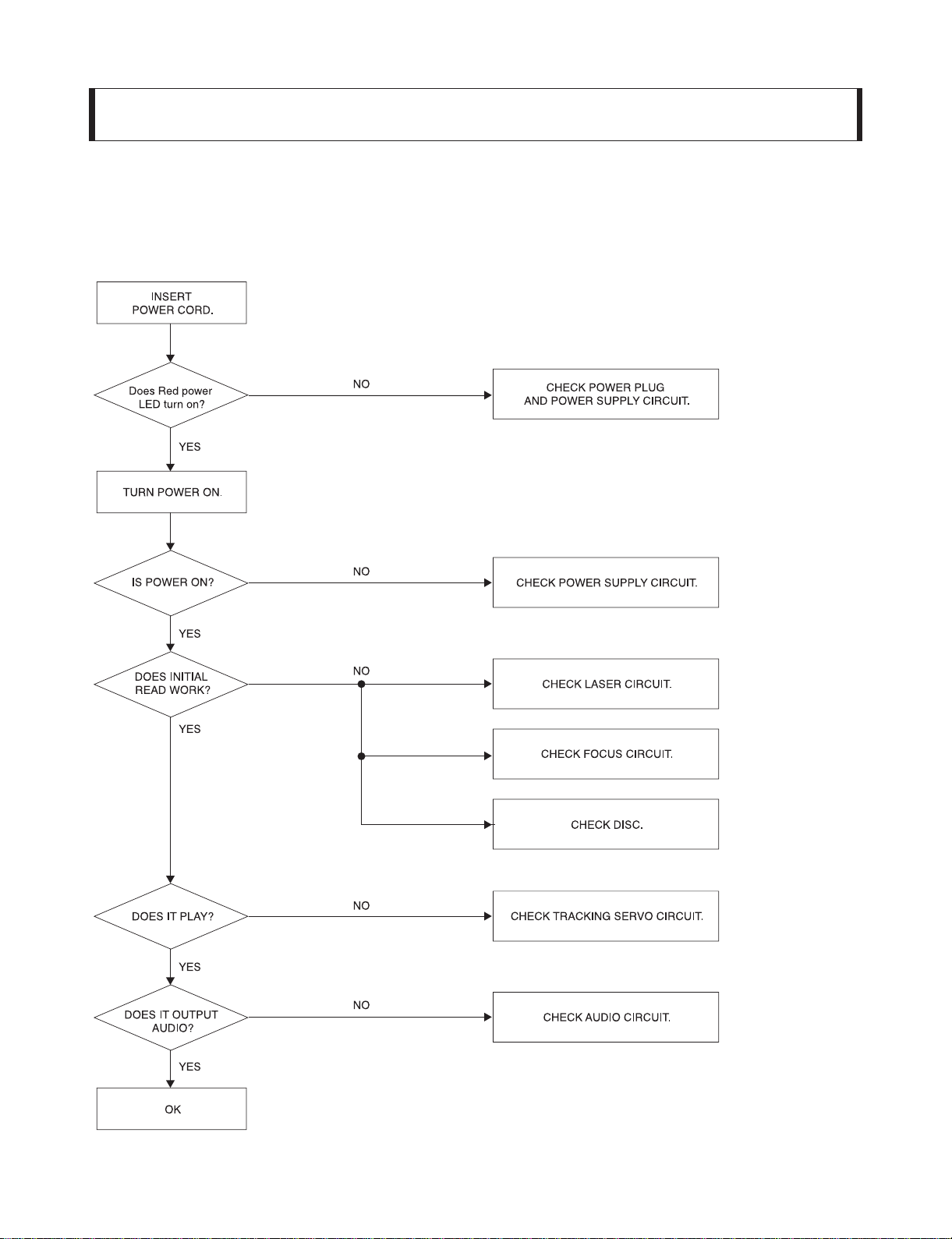
SECTION 2. AUDIO PART
AUDIO TROUBLESHOOTING GUIDE
1. POWER SUPPLY CIRCUIT
Page 9
2-2
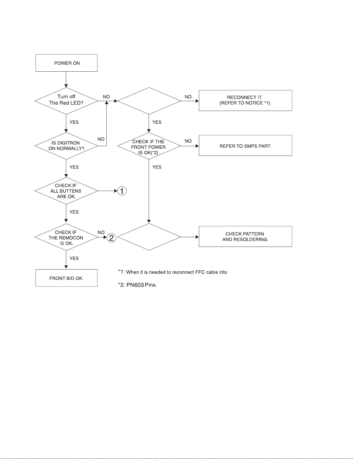
2. FRONT CIRCUIT (1/2)
THE P1301 IS OK?
CHECK IF
CHECK IF
THE DIS301 IS OK?
P1301
Short 1pin of CN901 with 4pin of CN901 in SMPS part.
PIN1
PIN2
PIN3
PIN12
: -41 VKK
: -22 FL+
: -26.5 FL-
: +5.0
Page 10
2-3
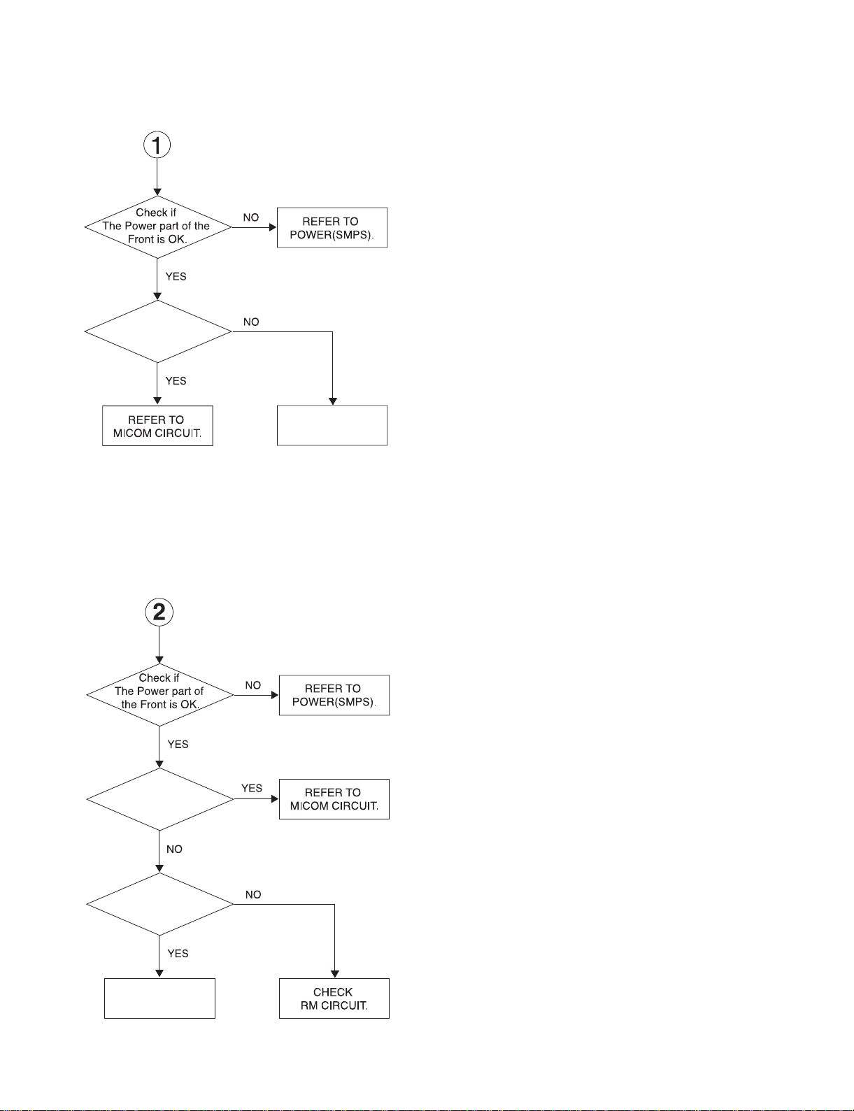
3. FRONT CIRCUIT (2/2)
CHECK IF
R345 ~ R350, R154
OK.
REPLACE
R345 ~ R350, R154.
Check if
the Remocon
waceform of the
P3101 pin 10
is OK
Check if
the RM301
voltage is OK(5V)
Resoldering or
Replace RM301
Page 11

Page 12
2-4 2-5
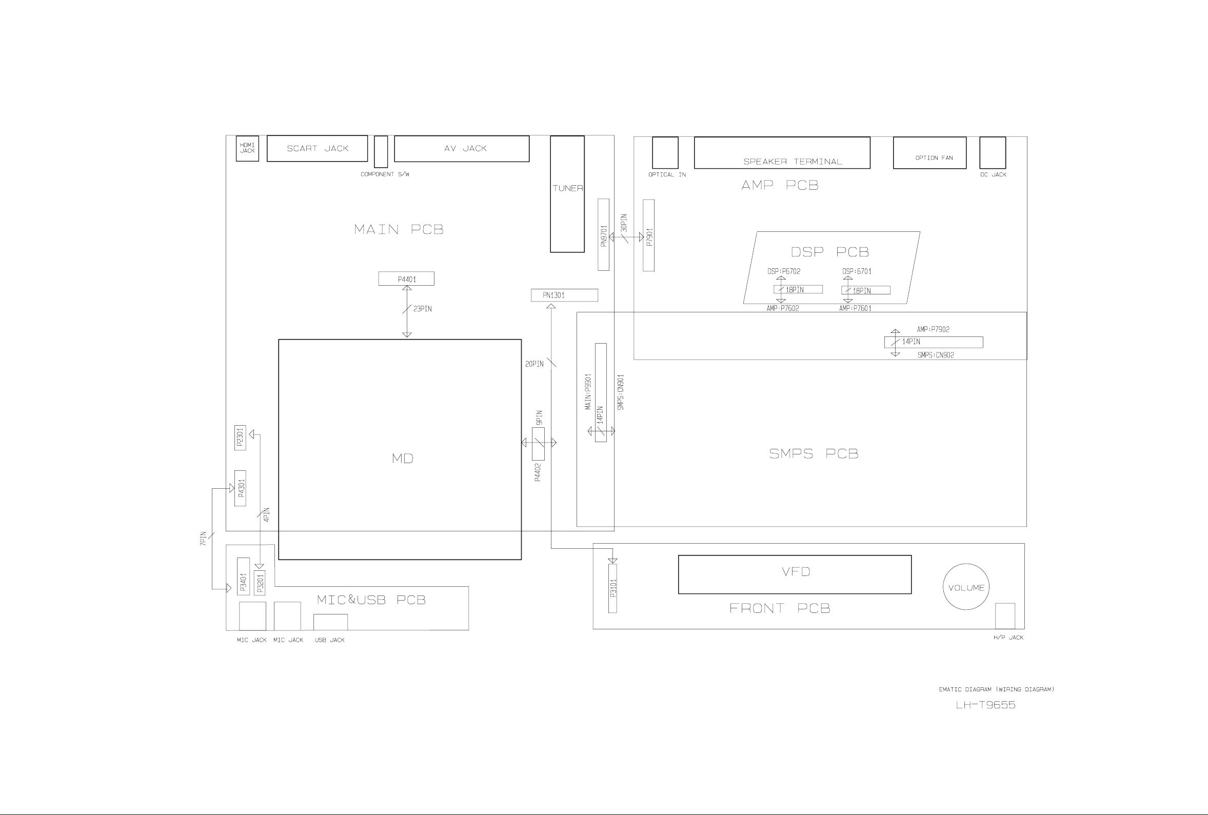
WIRING DIAGRAM
Page 13
2-6 2-7
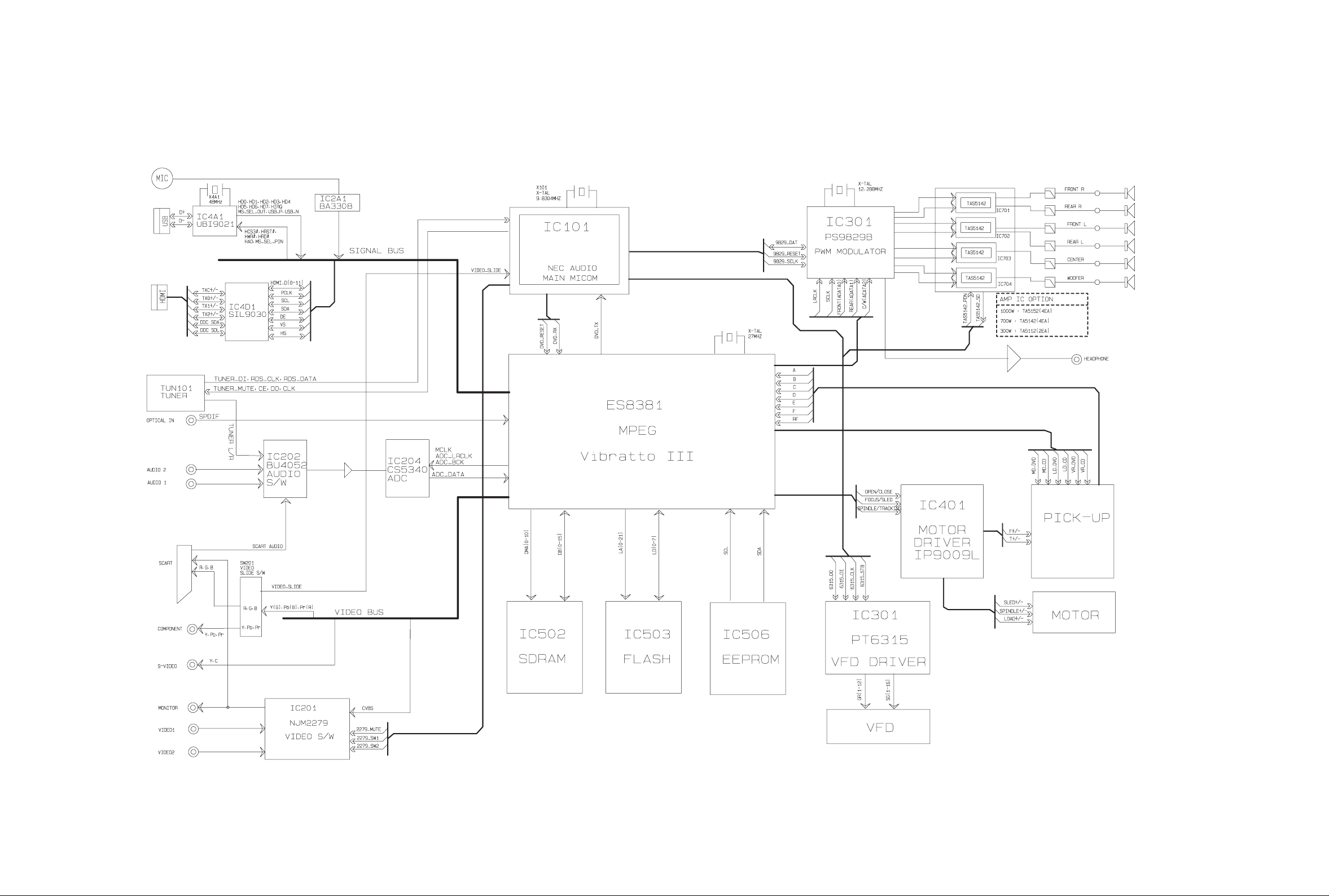
BLOCK DIAGRAM
Page 14
2-8 2-9
CIRCUIT DIAGRAMS
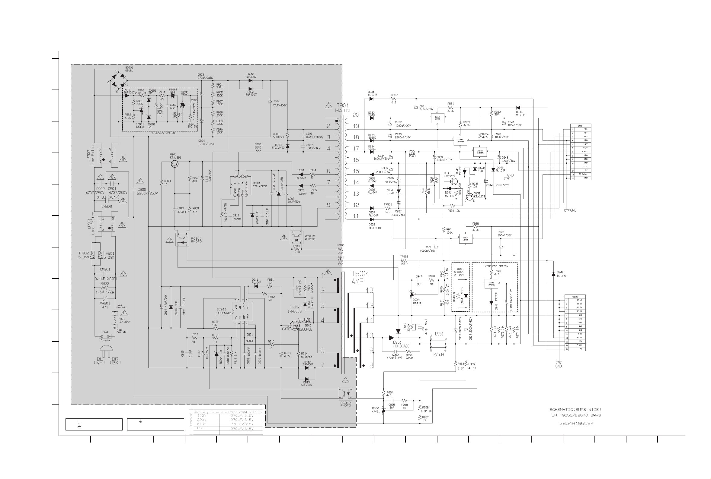
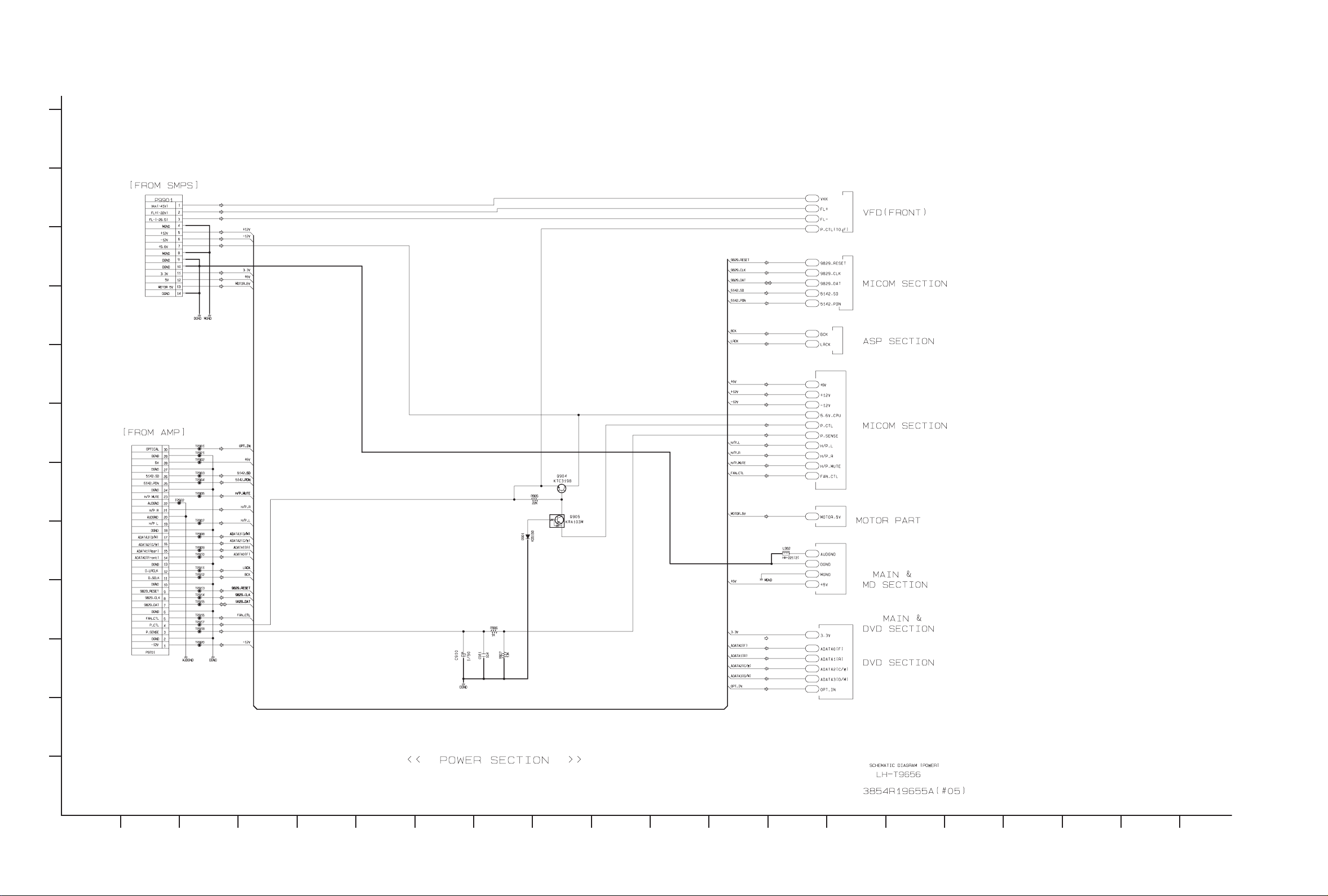
1. SMPS(POWER) CIRCUIT DIAGRAM (1000W, LH-T96’s)
NOTES) Symbol denotes AC ground.
NOTES) Symbol denotes DC chassis ground.
NOTE) Warning
NOTE) Parts that are shaded are critical
NOTE) With respect to risk of fire or
NOTE) electricial shock.
A
1
2
3
4
5
6
7
8
9
10
11
12
B C D E F G H I J K L M N O P Q R ST
Page 15
2-10 2-11
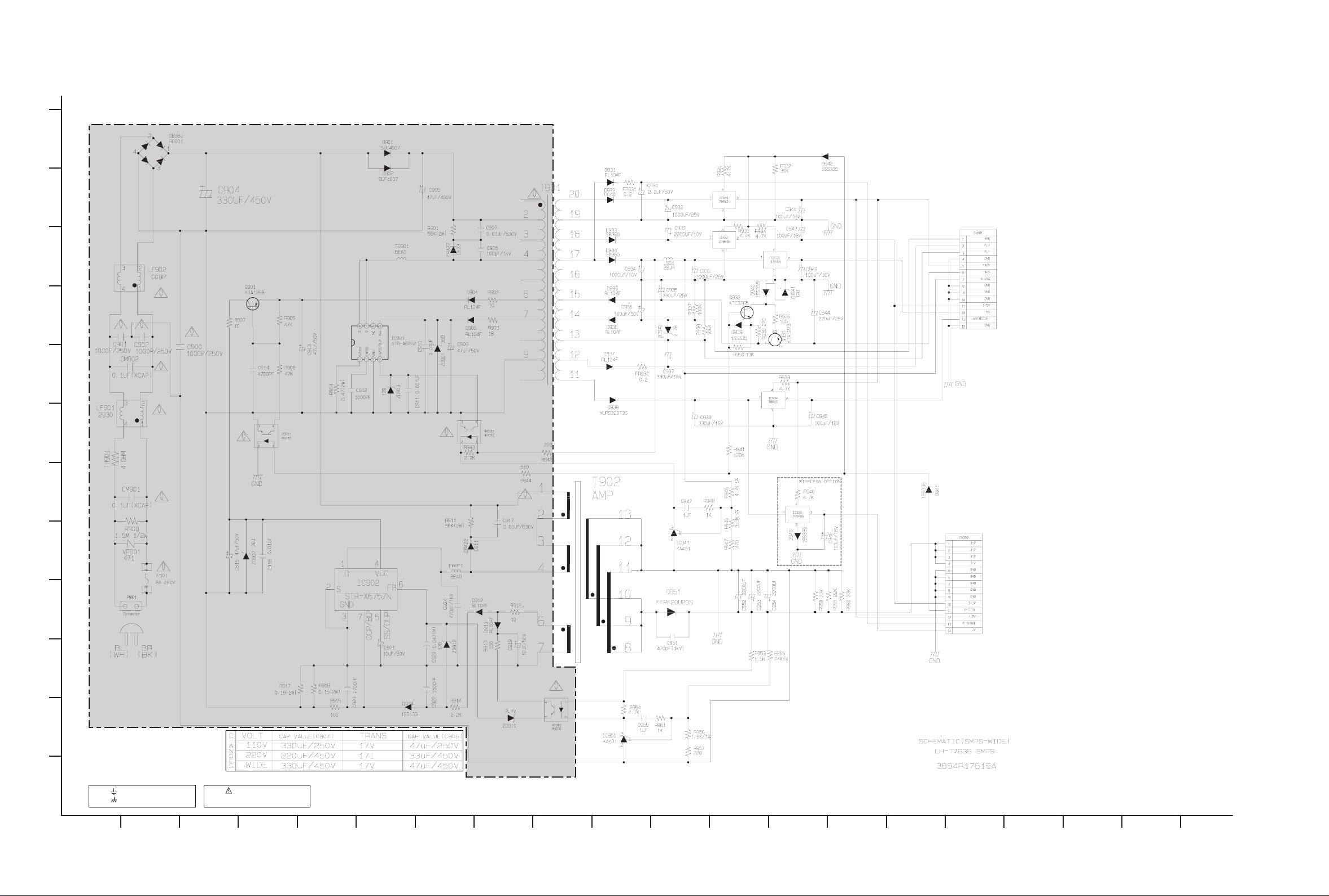
2. SMPS(POWER) CIRCUIT DIAGRAM (700W, LH-T76’s)
A
1
2
3
4
5
6
7
8
9
10
11
12
B C D E F G H I J K L M N O P Q R ST
NOTES) Symbol denotes AC ground.
NOTES) Symbol denotes DC chassis ground.
NOTE) Warning
NOTE) Parts that are shaded are critical
NOTE) With respect to risk of fire or
NOTE) electricial shock.
Page 16
2-12 2-13
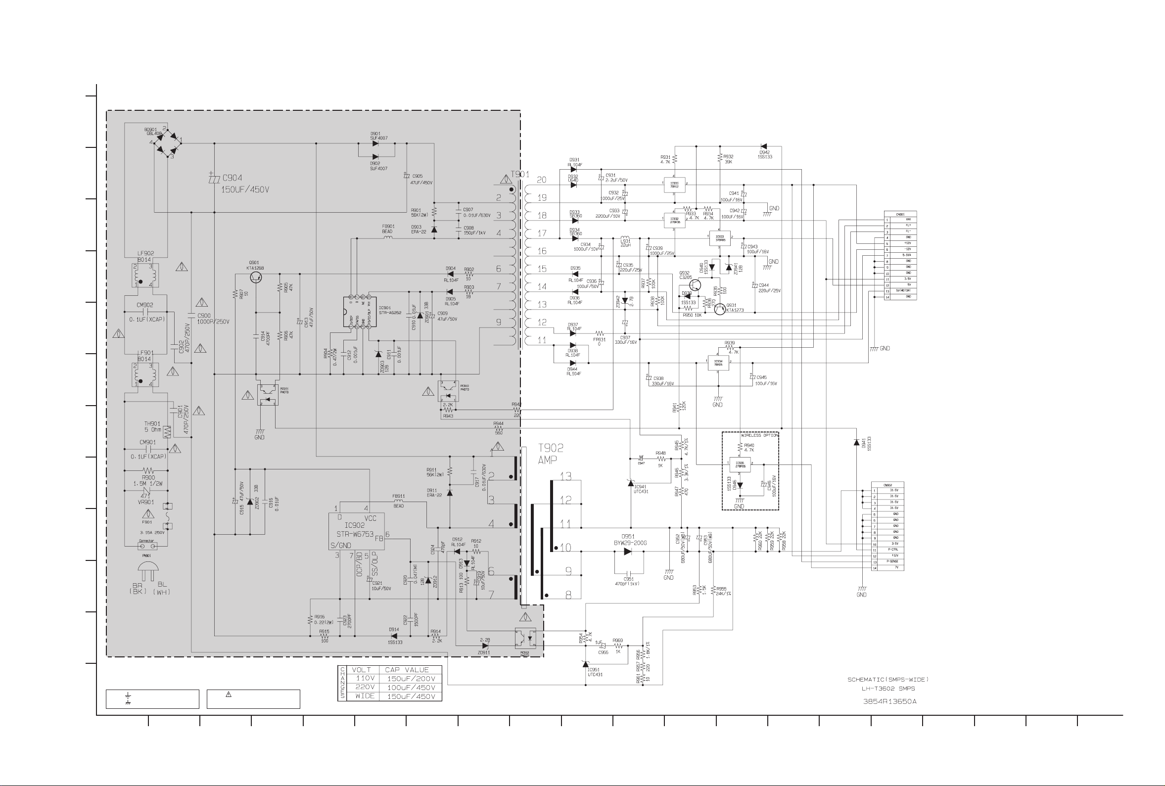
3. SMPS(POWER) CIRCUIT DIAGRAM (300W, LH-T36’s)
NOTES) Symbol denotes AC ground.
NOTES) Symbol denotes DC chassis ground.
NOTE) Warning
NOTE) Parts that are shaded are critical
NOTE) With respect to risk of fire or
NOTE) electricial shock.
A
1
2
3
4
5
6
7
8
9
10
11
12
B C D E F G H I J K L M N O P Q R ST
Page 17
2-14 2-15
4. POWER INTERFACE CIRCUIT DIAGRAM
A
1
2
3
4
5
6
7
8
9
10
11
12
B C D E F G H I J K L M N O P Q R ST
Page 18
2-16 2-17
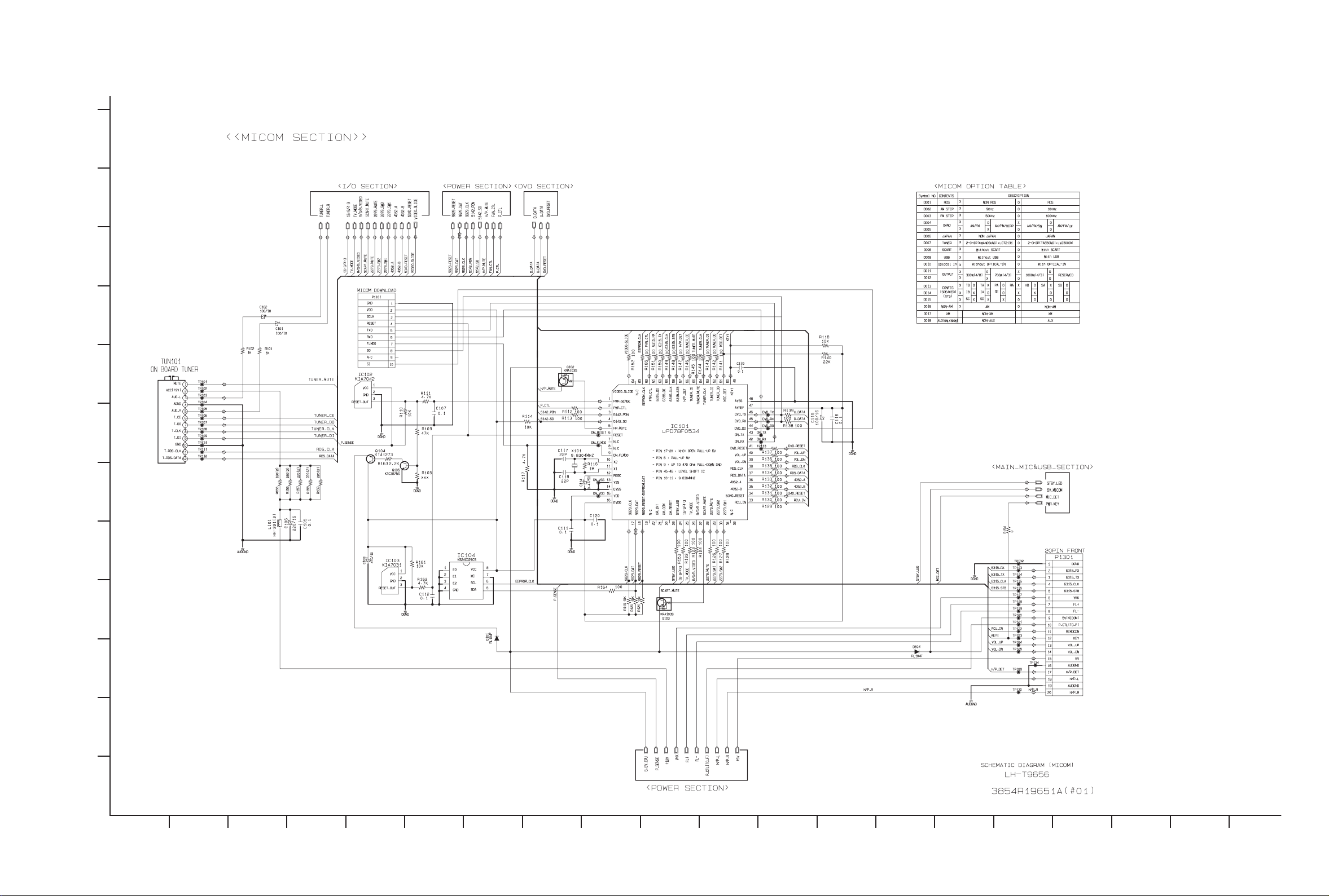
5. µ-COM(MAIN) CIRCUIT DIAGRAM
A
1
2
3
4
5
6
7
8
9
10
11
12
B C D E F G H I J K L M N O P Q R ST
Page 19
2-18 2-19
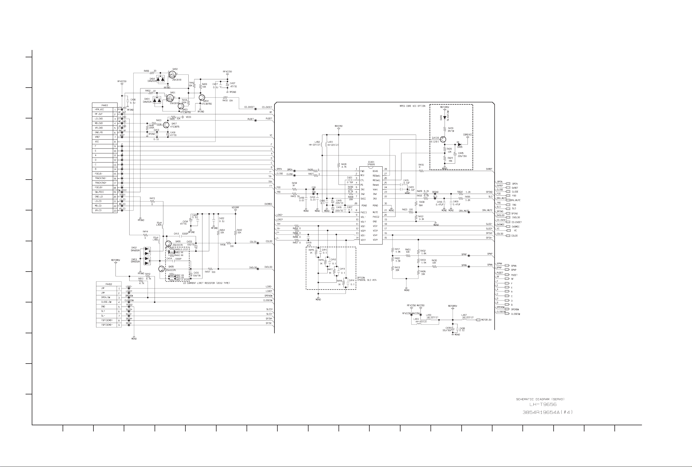
6. SERVO CIRCUIT DIAGRAM
A
1
2
3
4
5
6
7
8
9
10
11
12
B C D E F G H I J K L M N O P Q R ST
Page 20
2-20 2-21
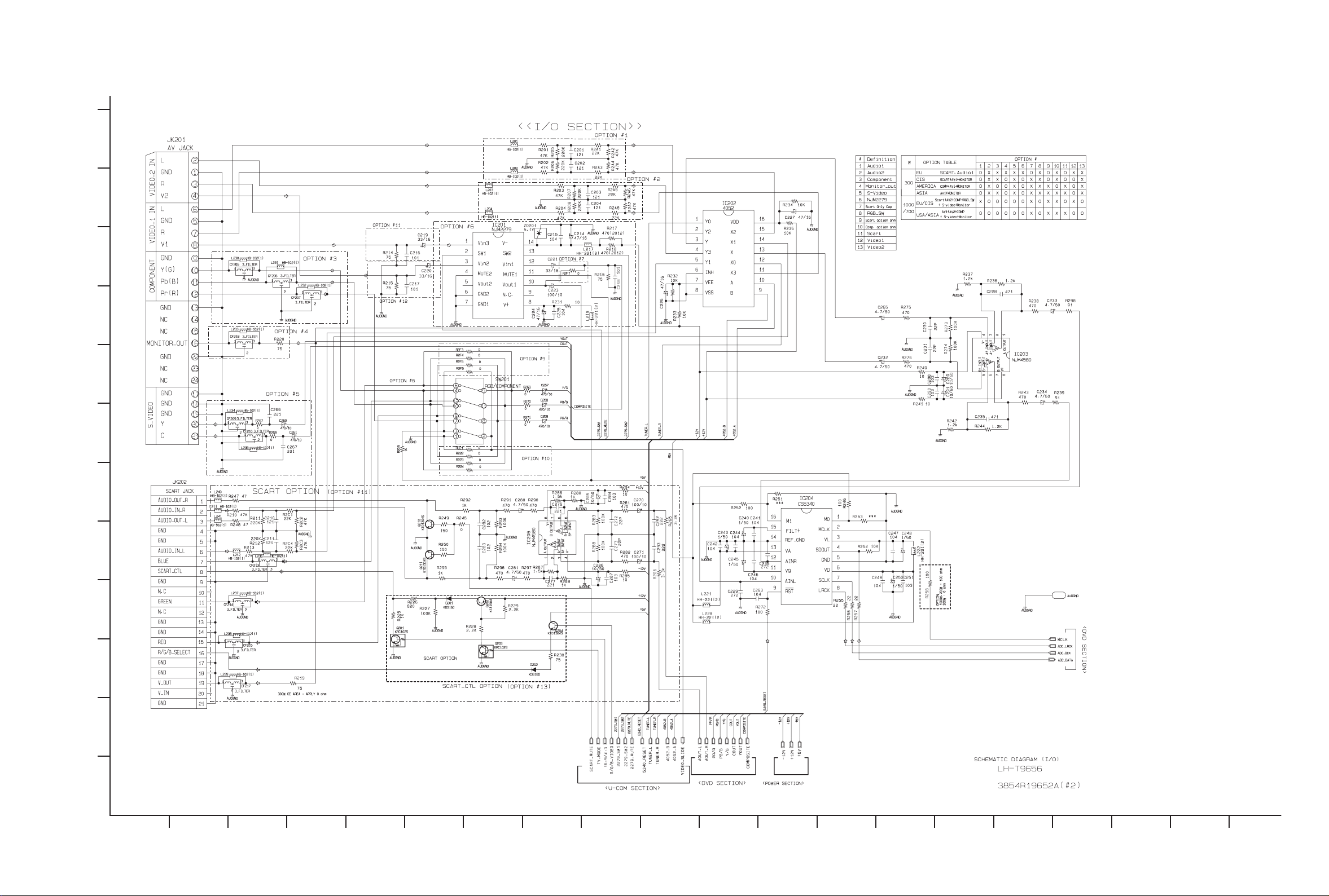
7. I/O CIRCUIT DIAGRAM
A
1
2
3
4
5
6
7
8
9
10
11
12
B C D E F G H I J K L M N O P Q R ST
Page 21

2-22 2-23
8. MIC CIRCUIT DIAGRAM
A
1
2
3
4
5
6
7
8
9
10
11
12
B C D E F G H I J K L M N O P Q R ST
Page 22

2-24 2-25
9. USB CIRCUIT DIAGRAM
A
1
2
3
4
5
6
7
8
9
10
11
12
B C D E F G H I J K L M N O P Q R ST
Page 23

2-26 2-27
10. MIC & USB CIRCUIT DIAGRAM
A
1
2
3
4
5
6
7
8
9
10
11
12
B C D E F G H I J K L M N O P Q R ST
Page 24

2-28 2-29
11. HDMI CIRCUIT DIAGRAM(OPTIONAL PART)
A
1
2
3
4
5
6
7
8
9
10
11
12
B C D E F G H I J K L M N O P Q R ST
Page 25

2-30 2-31
12. FRONT CIRCUIT DIAGRAM
A
1
2
3
4
5
6
7
8
9
10
11
12
B C D E F G H I J K L M N O P Q R ST
Page 26

2-32 2-33
PRINTED CIRCUIT BOARD DIAGRAMS
1. MAIN P.C. BOARD DIAGRAM ( TOP VIEW )
Page 27

2-34 2-35
2. MAIN P.C. BOARD DIAGRAM ( BOTTOM VIEW )
Page 28

2-36 2-37
3. SMPS P.C. BOARD (1000W, LH-T96’S)
( TOP VIEW )
( BOTTOM VIEW )
5. SMPS P.C. BOARD (300W, LH-T36’S)
4. SMPS P.C. BOARD (700W, LH-T76’S)
Page 29

2-38 2-39
6. KEY P.C. BOARD
7. TIMER P.C. BOARD
( BOTTOM VIEW )
( TOP VIEW )
( TOP VIEW )
( BOTTOM VIEW )
Page 30

3-1
ELECTRICAL TROUBLESHOOTING GUIDE
1. System operation flow
SECTION 3. DVD & AMP PART
Power On
1. 8082 initializes SERVO, DSP & RISC registers
2. Write RISC code to SDRAM
3. Reset RISC
Show LOGO
Yes
Tray Close to Closed position
SLED Moves to Inner Position
1. Judge whether have disc and disc type
2. Jump to related disc reading procedure
Tray Closed?
No
SLED at Inner
Side?
No
Recieve
OPEN/ CLOSE
Key?
Yes
No
1. Execute Pressed Key & IR Key
2. Systemoperati on Routi ne Loop
1. Stop Playback & Open Tray
2. Display tray open message & LOGO
No
Receive
CLOSE Key?
Yes
Page 31

3-2
2. Test & debug flow
TEST
Check the
AC Vol tage
Power PCBA (110V
or 220V)
Yes
Switch on the Power PCBA
Is the
DC Voltage
outputs OK? (-41V, -22V,
-26.5V, ±12V, 5.6V, 3.3V,
5V, 7V, 32.5V)
Yes
Are 3.3V and 5V DC
outputs normal on main
PCBA?
Yes
Update
FLASH
successfully?
No
No
No
No
Check the POWER PART
Check the POWER PART
Check the regulators or diode.
1. Check 27MHz system clock.
2. Check systemreset circuit.
3. Check FLASH R/Wenable signal PRD,
RWR.
4. Check FLASH Memory related circuit.
Yes
Replace FLASH
A
Page 32

3-3
A
ES8381
Check connection lines between
SDRAM(IC502) & ES8381 and
the SDRAM is damaged.
ES8381
VIDEO outputs
properly?
Normal
OPEN_SW,
CLOSE_SW
signal?
Check the related circuit of ES8381
IC501 Pins133, 134, 137, 138, 139, 140
Check the Tray control IO pins on
ES8381.
Check the Tray control amplifyung
circuit IC401.
Page 33

3-4
B
Motor
Driver DRV_MUTE
pin is High?
Motor
Driver DRV_MUTE
pin is High?
SLED+ and
SLED- output
properly?
Check the connection line of
DRV_MUTE
Check the related circuit of
SLEGN
Check Focus connection on
ES8381 and motor driver.
Page 34

3-5
C
Check the laser power circuit on
ES8381 and connecting to
power transistor.(Q405, Q406)
Collector
voltage of power
transistor is OK?
(Q405, Q406)
Proper
RF signal on ES8381
Check the RF connection
between IP9009 and ES8381.
Proper
SPINDLE signal on
ES8381
SPNP
SPNN output
properly?
Check the related circuit on
ES8381 RF signal.
ES8381.
Page 35

3-6
D
Proper
signals on A, B, C,
D of ES8381
Proper
CD-DVDCT signal
on ES8381
Check CD_DVDCT connection
between IP9009 and ES8381
Proper
CD-DVDCT signal
on ES8381
Proper
TRACK signal
on ES8381
Check connections between
ES8381 and pick-up head.
Check the related circuit on
ES8381 CD-DVDCT
Check the related circuit on
ES8381.
Check the TRACK connection
on ES8381 and motor driver.
TR+ & TR-
output properly?
Page 36

3-7
E
PWM IC
received correct data
stream?
Normal
PWM IC out?(IC601)
Check Digital Amp circuit
(IC701, IC702, IC703, IC704)
Check connection between
IC601 BCK, LRCK, ADATAO
Check the related circuit of
PWM.(Check Audio out
Pins54, 55, 58, 59, 61, 62,
67, 68, 70, 71, 74, 75
Page 37

3-8
3. AUDIO µ-COM Circuit(DVD & AMP)
YES
Does CD/DVD appear
at FLD?
Does AV1, TV Audio, AV1 opt.
and FM 87.5 appear at FLD
OK
Does Loading appear
at FLD?
POWER ON
YES NO
YES
Does no Disc or Time
appear at FLD?
NO YES
NO
NO
NO
NO
NO
NO
Does it appear DVD Error
at FLD?
Refer to SMPS.
Refer to oscillator Circuit.
Check IC101 Reset
Waveform.
Check 3.3V line.
Check Power section
Circuit.
NO
Check power part of Main
B/D.
Check oscillator of X101.
Check if IC101 Pin41
is high.
Check if IC101 Pin15, 16,
47 are high(5V).
Check if IC101 Pin1
is high.
Replace IC101.
NO
NO
Check if DVD an Audio
Micom Insert is OK.
Check Power.
YES
Check DVD Module.
YES
Check SMPS.
YES YES
YES
YES
YES
YES
YES
Page 38

3-9
DETAILS AND WAVEFORMS ON SYSTEM TEST AND DEBUGGING
1. SYSTEM 27MHz CLOCK,RESET,FLASH R/W SIGNAL
1) ES8381 main clock is at 27MHz(X501)
3.8V, 27MHz
FIG 1-1
2) ES8381 reset is high active.
PWR_CTL(SYSTEM µ-COM)
(IC101 PIN2)
5.2VA
Power Cord in
DVD_RESET(IC101 PIN 41)
MRST#(IC501 PIN 251)
FIG 1-2
Page 39

3-10
2. SDRAM CLOCK
1) ES8381 main clock is at 27MHz(X501)
(IC502 PIN 38)
DCLK = 93MHz, Vp-p=2.2, Vmax=2.7V
FIG 2-1
3) Flash R/W enable signal during download(Downloading)
FRD(IC503 PIN 28)
FWR(IC503 PIN 11)
FIG 1-4
Page 40

3-11
3. TRAY OPEN/CLOSE SIGNAL
1) Tray open/close waveform
OPENSW(P4402 PIN3)
CLOSESW(P4402 PIN4)
OPEN(IC401 PIN 1)
CLOSE(IC401 PIN 2)
FIG 3-1
2) Tray close waveform
OPENSW(P4402 PIN3)
CLOSESW(P4402 PIN4)
OPEN(IC401 PIN 1)
CLOSE(IC401 PIN 2)
FIG 3-2
Page 41

3-12
4. SLED CONTROL RELATED SIGNAL (NO DISC CONDITION)
SLO(2.0V/1.4V/1.0V)
(IC501 PIN 209)
DRV_MUTE(5V) – (IC401 PIN 21)
SLED+(4.7V/3.6V/1.9V)
(IC401 PIN 17)
SLED-(5.3V/3.7V/2.5V)
(IC401 PIN 18)
FIG 4-1
3) Tray open waveform
OPENSW(P4402 PIN3)
CLOSESW(P4402 PIN4)
OPEN(IC401 PIN 1)
CLOSE(IC401 PIN 2)
FIG 3-3
Page 42

3-13
5. LENS CONTROL RELATED SIGNAL(NO DISC CONDITION)
FOO(1.5V/1.4V/1.3V)
(IC501 PIN 208)
F+(4.0V/3.6V/3.2V)
(IC401 PIN 13)
F-(4.0V/3.6V/3.2V)
(IC401 PIN 14)
FIG 5-1
6. LASER POWER CONTROL RELATED SIGNAL(NO DISC CONDITION)
DVD MDI(0V/180mV)
(IC501 PIN 188)
DVDLDO501(5.0V//3.5V)
(IC501 PIN 185)
CDLDO(5.0V/3.6V)
(IC501 PIN 186)
FIG 6-1
Page 43

3-14
F+(IC401 PIN 13)
CD_DVDCT(IC501 PIN 169)
RF(IC501 PIN 196)
FIG 7-2 (DVD)
7. DISC TYPE JUDGEMENT WAVEFORMS
F+(IC401 PIN 13)
CD_DVDCT(IC501 PIN 169)
RF(IC501 PIN 196)
FIG 7-1 (DVD)
Page 44

3-15
F+(IC401 PIN 13)
CD_DVDCT(IC501 PIN 169)
RF(IC501 PIN 196)
FIG 7-3 (CD)
F+(IC401 PIN 13)
CD_DVDCT(IC501 PIN 169)
RF(IC501 PIN 196)
FIG 7-4 (CD)
Page 45

3-16
CD_DVDCT(IC501 PIN 169)
FOO(IC501 PIN208)
F+(IC401 PIN 13)
F-(IC401 PIN 14)
FIG 8-2 (CD)
8. FOCUS ON WAVEFORMS
CD_DVDCT(IC501 PIN 169)
FOO(IC501 PIN208)
F+(IC401 PIN 13)
F-(IC401 PIN 14)
FIG 8-1 (DVD)
Page 46

3-17
9. SPINDLE CONTROL WAVEFORMS (NO DISC CONDITION)
SPINO(1.4V/1.8V)
(IC501 PIN 207)
SP-(3.6V/2.4V)
(IC501 PIN 192)
SP+(3.6V/4.8V)
(IC501 PIN 191)
FIG 9-1
10. TRACKING CONTROL RELATED SIGNAL(System checking)
CD_DVDCT(IC501 PIN 169)
TRO(IC501 PIN 210)
TR-(IC401 PIN 12)
TR+(IC401 PIN 11)
FIG 10-1(DVD)
Page 47

3-18
CD_DVDCT(IC501 PIN 169)
TRO(IC501 PIN 210)
TR-(IC401 PIN 12)
TR+(IC401 PIN 11)
FIG 10-2(CD)
12. ES6698FD VIDEO OUTPUT WAVEFORMS
1) Full colorbar signal(COMPOSIT)
(IC501 PIN 134)
FIG 12-1
Page 48

3-19
2) Y
(IC501 PIN 140)
FIG 12-2
1) Audio L/R
FIG 13-1
13. AUDIO OUTPUT FROM PWM IC
(IC602 PIN 1, 7)
Page 49

3-20
BCK(IC501 PIN 155)
LRCK(IC501 PIN 156)
ASDATA3
2) Audio related Signal
ADATA0(IC501 PIN 154)
FIG 13-2
Page 50

3-21
1)
• R620 → TP611
or
R621 TP612
2)
• R618 → TP609
or
R619 TP610
3)
• R612 → TP603
or
R613 TP604
4)
• R610 → TP601
or
R611 TP602
5)
• R614 → TP605
or
R615 TP606
6)
• R616 → TP607
or
R617 TP608
14. DVD & AMP WAVEFORMS
Page 51

Page 52

A
1
2
3
4
5
6
7
8
9
10
11
12
B C D E F G H I J K L M N O P Q R ST
3-22 3-23
DVD & AMP CIRCUIT DIAGRAMS
1. MPEG CIRCUIT DIAGRAM
Page 53

A
1
2
3
4
5
6
7
8
9
10
11
12
B C D E F G H I J K L M N O P Q R ST
3-24 3-25
2. DSP CIRCUIT DIAGRAM
Page 54

3. AMP CIRCUIT DIAGRAM(700W/1000W, LH-T76/96’S)
A
1
2
3
4
5
6
7
8
9
10
11
12
B C D E F G H I J K L M N O P Q R ST
3-26 3-27
Page 55

3-28 3-29
4. AMP CIRCUIT DIAGRAM(300W, LH-T36’S)
A
1
2
3
4
5
6
7
8
9
10
11
12
B C D E F G H I J K L M N O P Q R ST
Page 56

PRINTED CIRCUIT BOARD DIAGRAMS
1. DSP P.C. BOARD DIAGRAM
3-30 3-31
( TOP VIEW ) ( BOTTOM VIEW )
Page 57

3-32 3-33
2. AMP P.C. BOARD DIAGRAM_300W (LH-T36’s)
( TOP VIEW ) ( BOTTOM VIEW )
Page 58

3-34 3-35
3. AMP P.C. BOARD DIAGRAM_700W/1000W (LH-T76’s / T96’s)
( TOP VIEW ) ( BOTTOM VIEW )
Page 59

• CABINET AND MAIN FRAME SECTION_LH-TK36’s
4-1 4-2
SECTION 4. EXPLODED VIEWS
P3401
P3201
OPTIONAL
PART
A50
MIC
275
465
283
A00
465
275
465
A46
463
MAIN
463
OPTIONAL
PART
473
468
463
CABLE1
AMP
DSP
A48
463
463
463
463
NOTES) THE EXCLAMATION POINT WITHIN AN
EQUILATERAL TRIANGLE IS INTENDED
TO ALERT THE SERVICE PERSONNEL
TO THE PRESENCE OF IMPORTANT
SAFETY INFORMATION IN SERVICE
LITERATURE.
OPTIONAL PART
463
250
A43
279
A44
261
CABLE2
264
SMPS
330
261
465
465
320
A47
271
A45
473
300
465
Page 60

4-3 4-4
• DECK MECHANISM EXPLODED VIEW(DP-10T)
012
019
013
017
439
014
435
015
018
015B
015A
016
012
440
030
001
002
003
432
A01
A02
020
012A
010
026
A03
036
025
024
431
435
012A
021
430
Page 61

Page 62

4-5
• Packing Accessory Section
827
MICRO PHONE
826
FILTER(CIRC)
808
BATTERY
900
REMOCON
803
PACKING, CASING
OPTIONAL PART
811
PLUG ASS'Y 1WAY(YELLOW)
824
ANTENNA LOOP(AM)
825
ANTENNA (FM)
INSTRUCTION ASSEMBLY
801
828
AC ADAPTOR
PACKING, CASING
803
804
BAG
802
BOX
832
DISC
Page 63

Page 64

5-1
SECTION 5. SPEAKER SECTION
1. LHS-36SE
• FRONT/REAR/CENTER SPEAKER(LHS-36SES)
852
850
A80
853
851
Page 65

5-2
• LHS-36SE
• PASSIVE SUBWOOFER SPEAKER(LHS-36SEW)
953
A90
956
955
951
950
952
954
 Loading...