

Page 1

- 1-1 -
SECTION 1. GENERAL
• SERVICING PRECAUTIONS
.......................................................................................................
1-2
• ESD PRECAUTIONS
...................................................................................................................
1-4
• SPECIFICATIONS
........................................................................................................................
1-5
• LOCATION OF CUSTOMER CONTROLS
...................................................................................
1-6
SECTION 2. AUDIO PART
• BLOCK DIAGRAM
........................................................................................................................
2-1
• SCHEMATIC DIAGRAMS
............................................................................................................
2-3
• WIRING DIAGRAM
....................................................................................................................
2-15
• VOLTAGE SHEET (IC&TR) ........................................................................................................ 2-17
• PRINTED CIRCUIT DIARGAMS
................................................................................................
2-21
SECTION 3. DVD PART
• DVD PART ELECTRICAL TROUBLESHOOTING GUIDE
..........................................................
3-1
• DETAILS AND WAVEFORMS ON SYSTEM TEST AND DEBUGGING ...................................... 3-8
• DVD PART SCHEMATIC DIAGRAMS
........................................................................................
3-21
• VOLTAGE SHEET (IC & TR)
......................................................................................................
3-27
• PRINTED CIRCUIT DIAGRAM
...................................................................................................
3-29
SECTION 4. EXPLODED VIEWS
......................................................................................
4-1
SECTION 5. SPEAKER PART
..........................................................................................
5-1
SECTION 6. REPLACEMENT PARTS LIST
.....................................................................
6-1
CONTENTS
Page 2
SECTION 1. GENERAL PART
❏
SERVICING PRECAUTIONS
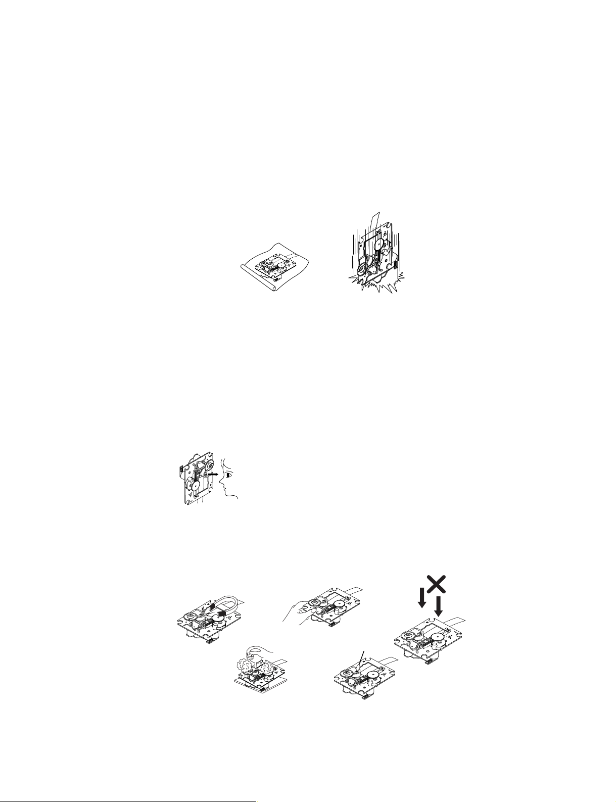
NOTES REGARDING HANDLING OF THE PICK-UP
1. Notes for transport and storage
1) The pick-up should always be left in its conductive bag until immediately prior to use.
2) The pick-up should never be subjected to external pressure or impact.
2. Repair notes
1) The pick-up incorporates a strong magnet, and so should never be brought close to magnetic materials.
2) The pick-up should always be handled correctly and carefully, taking care to avoid external pressure and
impact. If it is subjected to strong pressure or impact, the result may be an operational malfunction and/or
damage to the printed-circuit board.
3) Each and every pick-up is already individually adjusted to a high degree of precision, and for that reason
the adjustment point and installation screws should absolutely never be touched.
4) Laser beams may damage the eyes!
Absolutely never permit laser beams to enter the eyes!
Also NEVER switch ON the power to the laser output part (lens, etc.) of the pick-up if it is damaged.
5) Cleaning the lens surface
If there is dust on the lens surface, the dust should be cleaned away by using an air bush (such as used
for camera lens). The lens is held by a delicate spring. When cleaning the lens surface, therefore, a
cotton swab should be used, taking care not to distort this.
6) Never attempt to disassemble the pick-up.
Spring by excess pressure. If the lens is extremely dirty, apply isopropyl alcohol to the cotton swab. (Do
not use any other liquid cleaners, because they will damage the lens.) Take care not to use too much of
this alcohol on the swab, and do not allow the alcohol to get inside the pick-up.
- 1-2 -
Storage in conductive bag
Drop impact
NEVER look directly at the laser beam, and don’t let
contact fingers or other exposed skin.
Magnet
How to hold the pick-up
Pressure
Pressure
Cotton swab
Conductive Sheet
Page 3
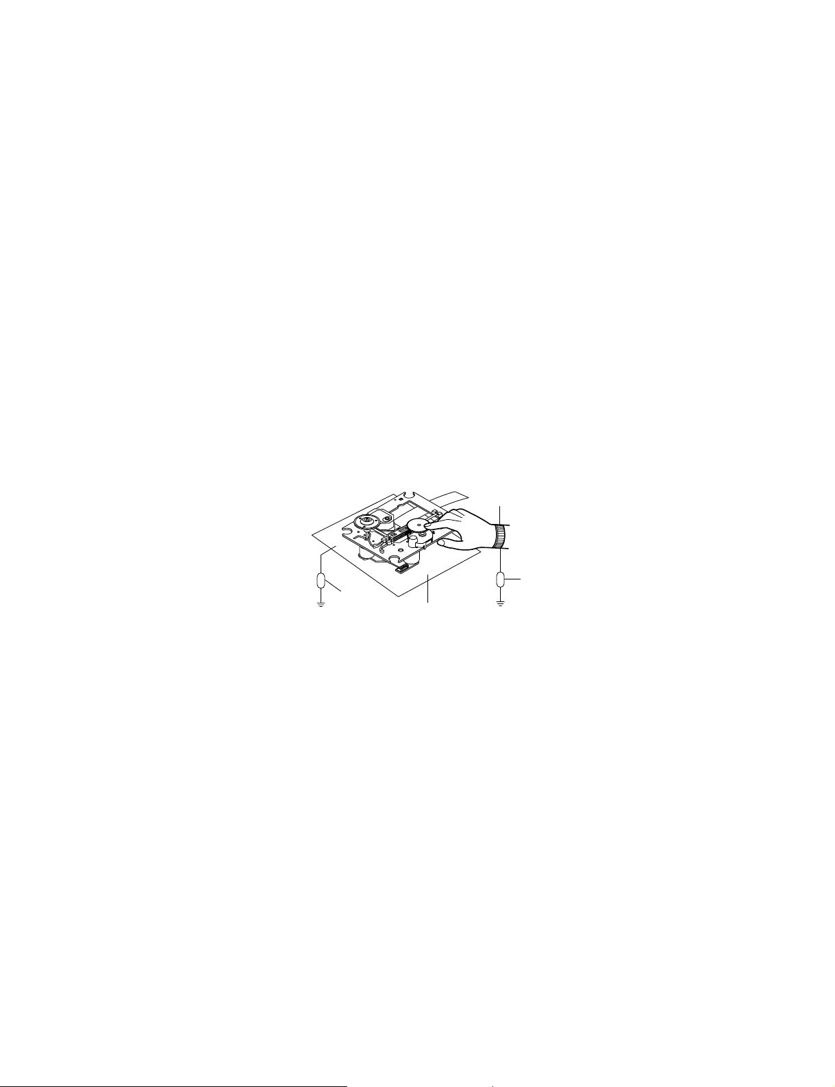
NOTES REGARDING COMPACT DISC PLAYER REPAIRS
1. Preparations
1) Compact disc players incorporate a great many ICs as well as the pick-up (laser diode). These
components are sensitive to, and easily affected by, static electricity. If such static electricity is high
voltage, components can be damaged, and for that reason components should be handled with care.
2) The pick-up is composed of many optical components and other high-precision components. Care must
be taken, therefore, to avoid repair or storage where the temperature of humidity is high, where strong
magnetism is present, or where there is excessive dust.
2. Notes for repair
1) Before replacing a component part, first disconnect the power supply lead wire from the unit
2) All equipment, measuring instruments and tools must be grounded.
3) The workbench should be covered with a conductive sheet and grounded.
When removing the laser pick-up from its conductive bag, do not place the pick-up on the bag. (This is
because there is the possibility of damage by static electricity.)
4) To prevent AC leakage, the metal part of the soldering iron should be grounded.
5) Workers should be grounded by an armband (1MΩ)
6) Care should be taken not to permit the laser pick-up to come in contact with clothing, in order to prevent
static electricity changes in the clothing to escape from the armband.
7) The laser beam from the pick-up should NEVER be directly facing the eyes or bare skin.
- 1-3 -
Armband
Conductive
Sheet
Resistor
(1 Mohm)
Resistor
(1 Mohm)
Page 4
❏
ESD PRECAUTIONS
Electrostatically Sensitive Devices (ESD)
Some semiconductor (solid state) devices can be damaged easily by static electricity. Such components
commonly are called Electrostatically Sensitive Devices (ESD). Examples of typical ESD devices are integrated
circuits and some field-effect transistors and semiconductor chip components. The following techniques should
be used to help reduce the incidence of component damage caused by static electricity.
1. Immediately before handling any semiconductor component or semiconductor-equipped assembly, drain off
any electrostatic charge on your body by touching a known earth ground. Alternatively, obtain and wear a
commercially available discharging wrist strap device, which should be removed for potential shock reasons
prior to applying power to the unit under test.
2. After removing an electrical assembly equipped with ESD devices, place the assembly on a conductive
surface such as aluminum foil, to prevent electrostatic charge buildup or exposure of the assembly.
3. Use only a grounded-tip soldering iron to solder or unsolder ESD devices.
4. Use only an anti-static solder removal device. Some solder removal devices not classified as "anti-static" can
generate electrical charges sufficient to damage ESD devices.
5. Do not use freon-propelled chemicals. These can generate electrical charges sufficient to damage ESD
devices.
6. Do not remove a replacement ESD device from its protective package until immediately before you are ready
to install it. (Most replacement ESD devices are packaged with leads electrically shorted together by
conductive foam, aluminum foil or comparable conductive materials).
7. Immediately before removing the protective material from the leads of a replacement ESD device, touch the
protective material to the chassis or circuit assembly into which the device will by installed.
CAUTION : BE SURE NO POWER IS APPLIED TO THE CHASSIS OR CIRCUIT, AND OBSERVE ALL OTHER
SAFETY PRECAUTIONS.
8. Minimize bodily motions when handing unpackaged replacement ESD devices. (Otherwise harmless motion
such as the brushing together of your clothes fabric or the lifting of your foot from a carpeted floor can
generate static electricity sufficient to damage an ESD device).
CAUTION. GRAPHIC SYMBOLS
- 1-4 -
THE LIGHTNING FLASH WITH APROWHEAD SYMBOL. WITHIN AN EQUILATERAL
TRIANGLE, IS INTENDED TO ALERT THE SERVICE PERSONNEL TO THE PRESENCE OF
UNINSULATED “DANGEROUS VOLTAGE” THAT MAY BE OF SUFFICIENT MAGNITUDE TO
CONSTITUTE A RISK OF ELECTRIC SHOCK.
THE EXCLAMATION POINT WITHIN AN EQUILATERAL TRIANGLE IS INTENDED TO
ALERT THE SERVICE PERSONNEL TO THE PRESENCE OF IMPORTANT SAFETY
INFORMATION IN SERVICE LITERATURE.
Page 5
- 1-6 -
❏
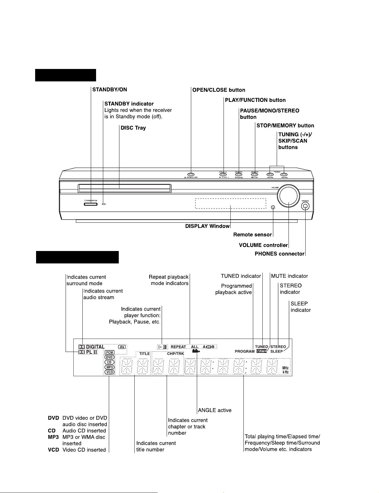
LOCATION OF CUSTOMER CONTROLS
FRONT PANEL
DISPLAY WINDOW
Page 6
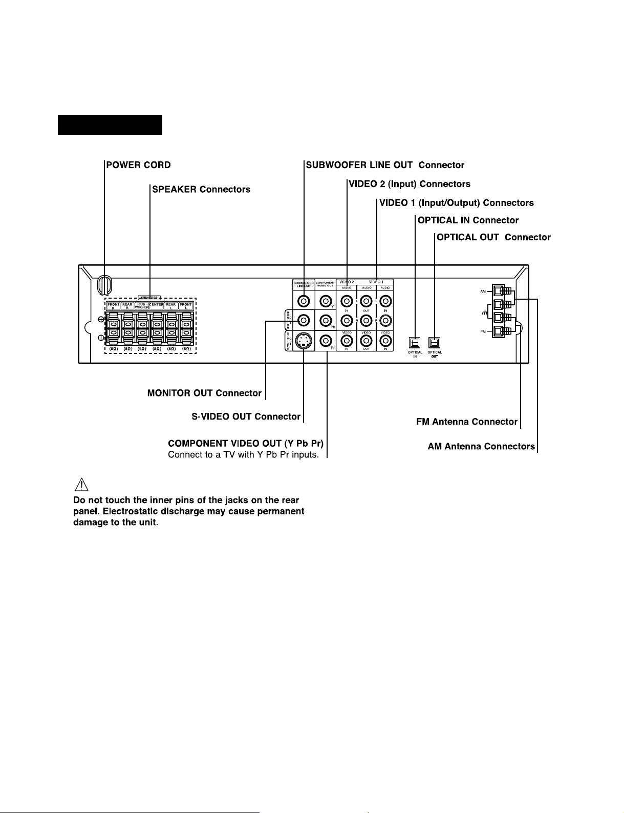
- 1-7 -
REAR PANEL
Page 7
- 1-8 -
AUDIO ELECTRICAL TROUBLESHOOTING GUIDE
INSERT
POWER CORD.
TURN ON
THE RED LED?
IS POWER ON?
CHECK POWER PLUG
AND POWER SUPPLY CIRCUIT.
DOES INITIAL
READ WORK?
DOES IT PLAY?
YES
NO
YES
YES
OK
NO
YES
NO
NO
CHECK POWER SUPPLY CIRCUIT.
CHECK LASER CIRCUIT.
CHECK TRACKING SERVO CIRCUIT.
TURN POWER ON.
CHECK FOCUS CIRCUIT.
CHECK DISC.
DOES IT OUTPUT
AUDIO?
YES
NO
CHECK AUDIO CIRCUIT.
1.
1.1.
1.
Page 8
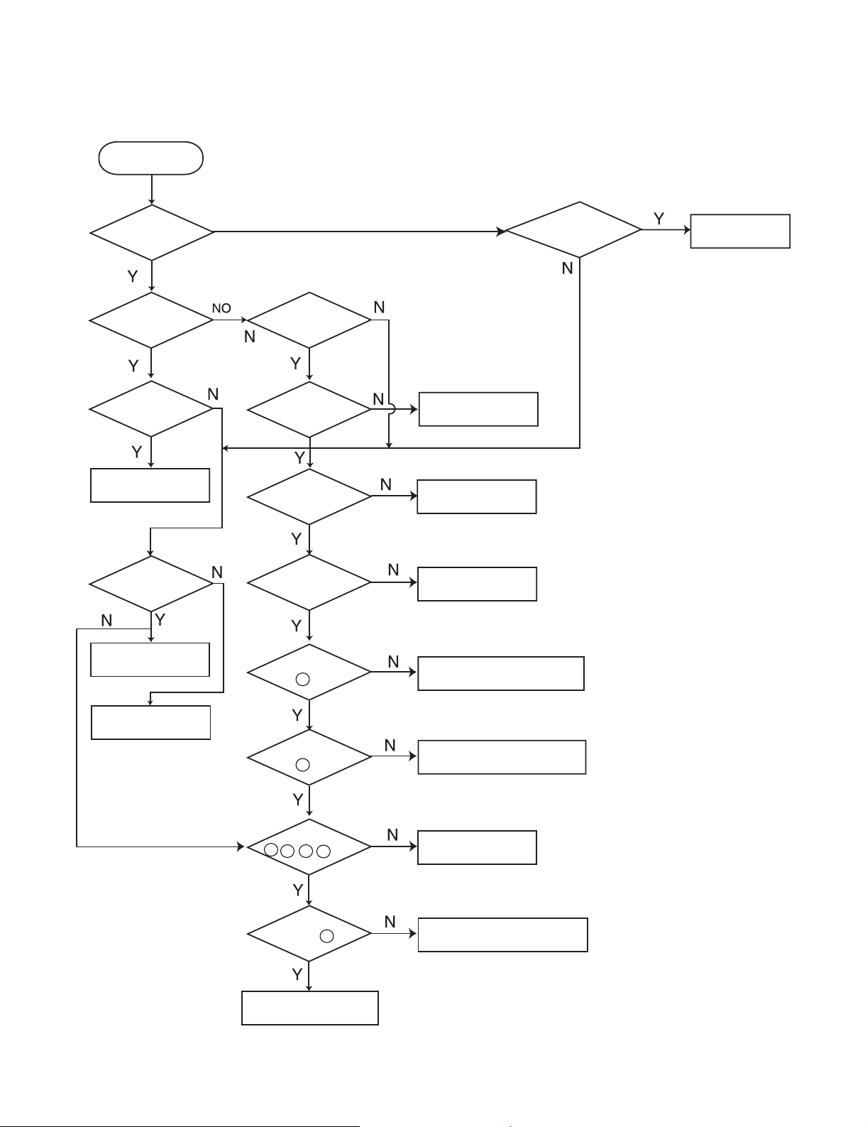
- 1-9 -
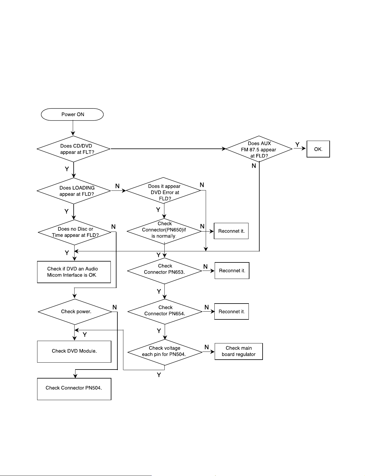
2. AUDIO µ. COM CIRCUIT
POWER ON
Does CD/DVD
appear at FLT?
Does LOADING
appear at FLD?
Does it appear
DVD Error at
FLD?
Does Video1/2, TV
AUDIO, FM 87.5
appear at FLD?
OK.
Check
Connector(PN903)if
is normally.
Reconnet it.
Refer to SMPS
Refer to oscillator
Circuit.
Check DVD Reset Waveform.
Check IC101 Reset Wavefrom.
Check 3.3V line.
Check Power dection Circuit..
Check power part
of Main B/D.
Check oscillator
of x101.
Check if PN200
PIN is High.
Check if IC101
PIN is High.
Check if IC101 PIN
, , , is high
(5V).
Check if IC101
PIN
is High .
Replace IC101.
Does no Dise or
Time appear at FLD?
Check if DVD an Audio
Micom Interface is OK.
Check power.
Check DVD Module.
Check SMPS.
17
46 72
90
11
5
26
Page 9
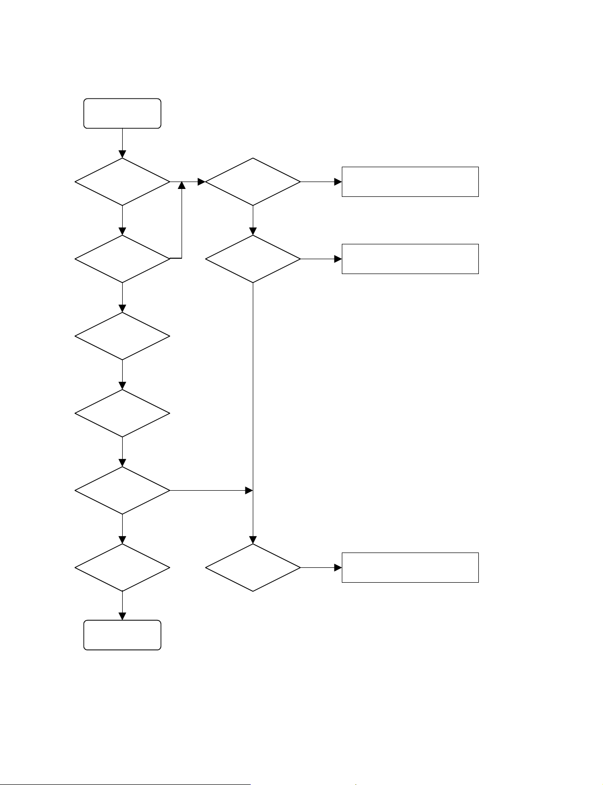
- 1-10 -
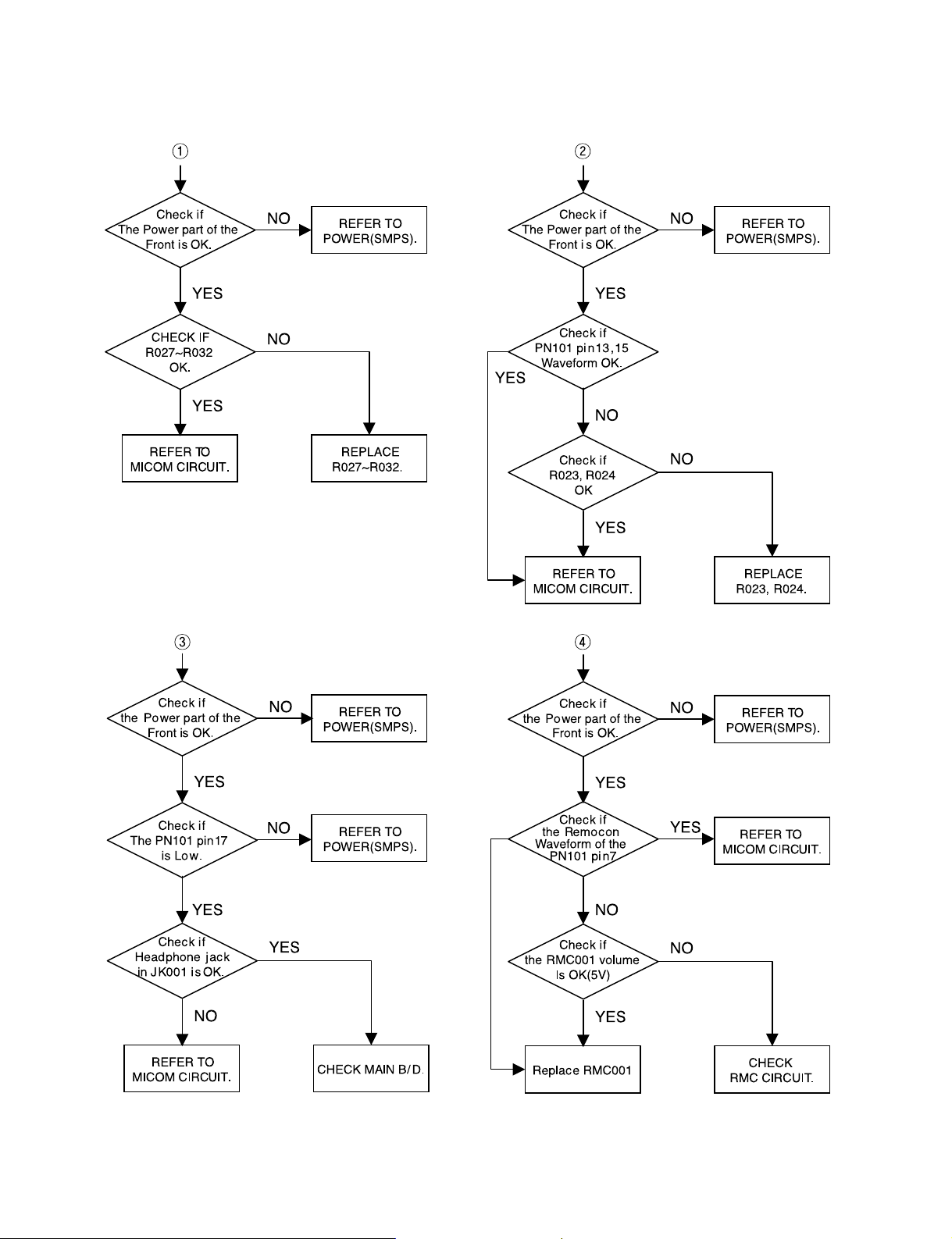
3. FRONT CIRCUIT (1/2)
POWER ON
TURN ON
THE GREEN LED?
CHECK IF THE
FRONT POWER
IS OK(*2).
IS DIGITRON
ON NORMALLY?
CHECK IF
THE HEADPHONE
IS OK.
YES
NO
YES
NO
YES
REFER TO SMPS PART.
CHECK IF
THE REMOCON
IS OK.
YES
CHECK IF
THE PN101/PN102
IS OK?
RECONNECT IT.
(REFER TO NOTICE *1).
CHECK IF
ALL BUTTENS
ARE OK.
YES
CHECK IF
THE VOLUME IS
OK.
YES
FRONT B/D OK.
YES
CHECK IF
THE VFD001 PINS
ARE OK.
CHECK PATTERN
AND RESOLDERING.
NO
YES
*1: When it i s needed to reconnect FPC cable into PN101/PN102,
short ZD972 + and screw(chassis GND) near to ZD972.
*2: PN101 Pins
PIN2 : -23.0V
PIN3 : -27.5V
PIN4 : 5.0V
PIN11 : -34.0V
PIN20 : 12.0V
NO
NO
Page 10
- 1-11 -
4. FRONT CIRCUIT (2/2)
Page 11
- 3-1 -
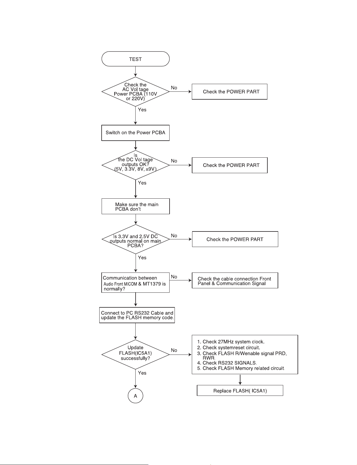
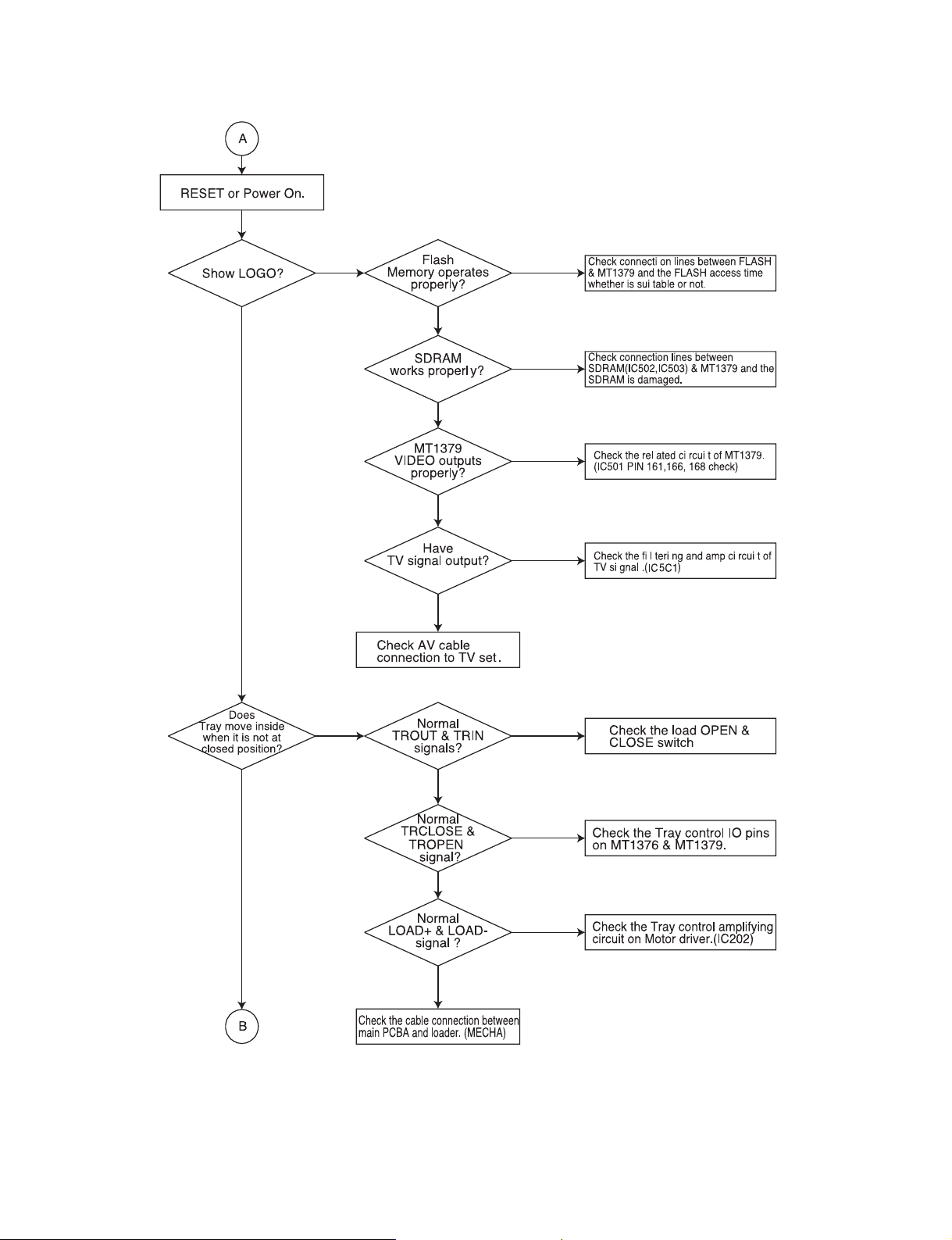
SECTION 3. DVD PART ELECTRICAL
TROUBLESHOOTING GUIDE
1. Power check flow
Page 12
- 3-2 -
2. Test & debug flow
Page 13
- 3-3 -
Page 14
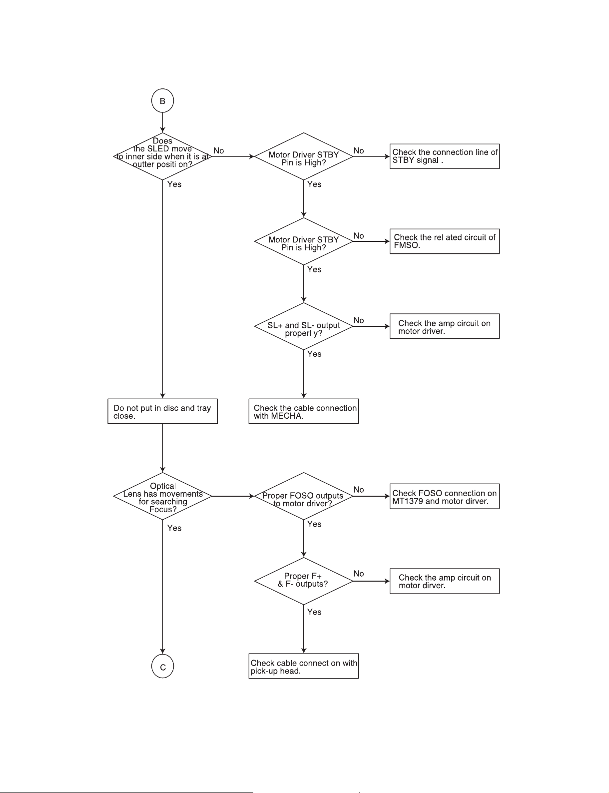
- 3-4 -
Page 15
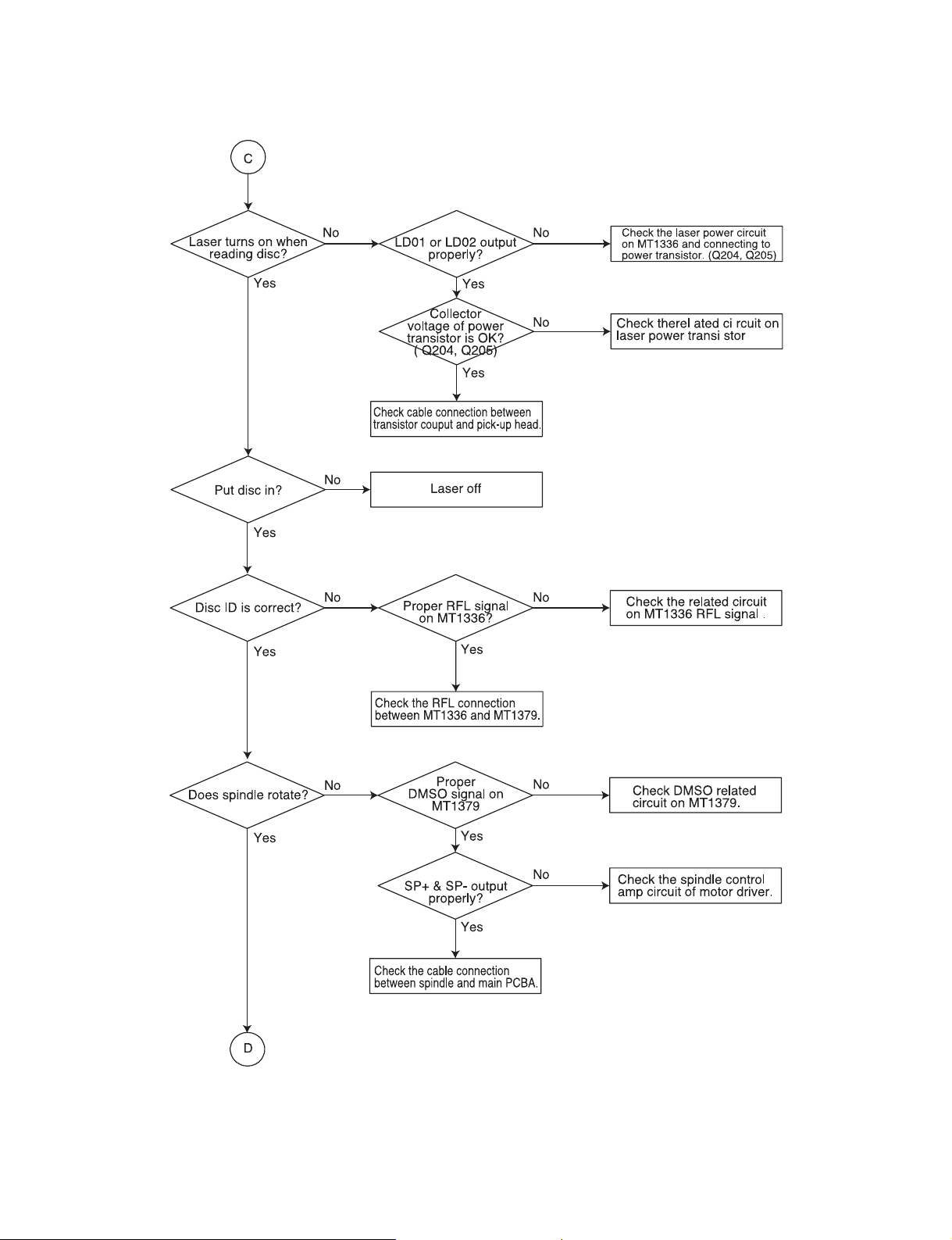
- 3-5 -
Page 16
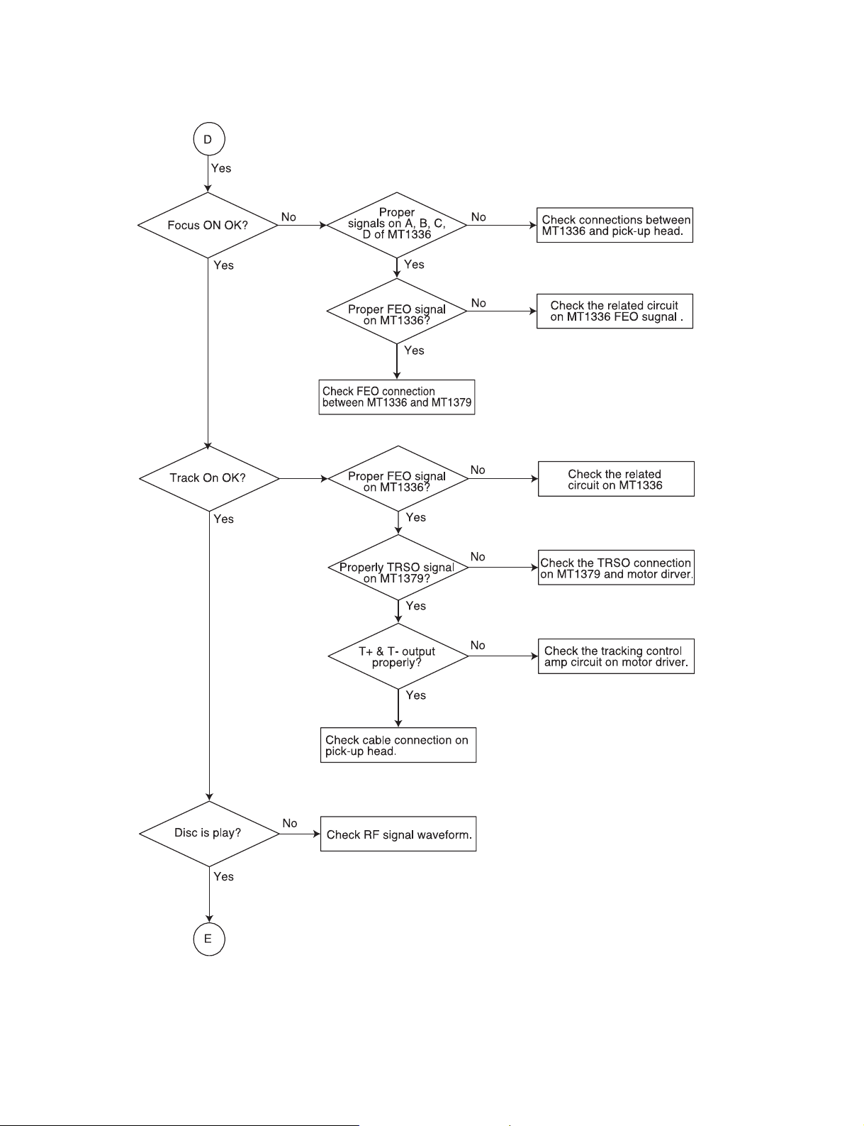
- 3-6 -
Page 17
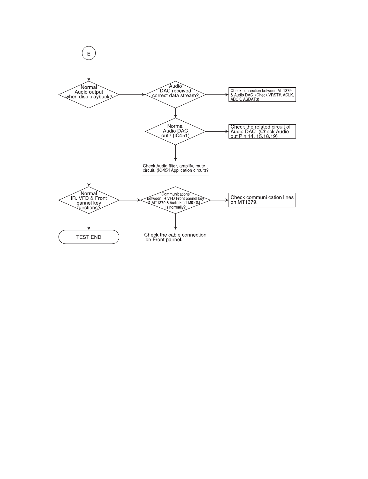
- 3-7 -
Page 18

- 3-8 -
❏
DETAILS AND WAVEFORMS ON SYSTEM TEST
AND DEBUGGING
1. SYSTEM 27MHz CLOCK,RESET,FLASH R/W SIGNAL
1) MT1379 main clock is at 27MHz(X501)
2) MT1336 reset is high active
Page 19

- 3-9 -
3) RS232 waveform during procedure(Downloading)
4) Flash R/W enable signal during download(Downloading)
Page 20

- 3-10 -
2. SDRAM CLOCK
1) MT1379 main clock is at 27MHz(X501)
3. TRAY OPEN/CLOSE SIGNAL
1) Tray open/close waveform
Page 21

- 3-11 -
2) Tray close waveform
3) Tray open waveform
Page 22

- 3-12 -
4. SLED CONTROL RELATED SIGNAL (NO DISC CONDITION)
5. LENS CONTROL RELATED SIGNAL(NO DISC CONDITION)
Page 23

- 3-13 -
6. LASER POWER CONTROL RELATED SIGNAL
(NO DISC CONDITION)
7. DISC TYPE JUDGEMENT WAVEFORM
Page 24

- 3-14 -
Page 25

- 3-15 -
8. FOCUS ON WAVEFORM
Page 26

- 3-16 -
9. SPINDLE CONTROL WAVEFORM (NO DISC CONDITION)
Page 27

- 3-17 -
10. TRACKING CONTROL RELATED SIGNAL(System checking)
Page 28

- 3-18 -
11. RF WAVEFORM
12. MT1379 AUDIO OPTICAL AND COAXIAL OUTPUT (ASPDIF)
Page 29

- 3-19 -
13. MT1379 VIDEO OUTPUT WAVEFORM
1) Full colorbar signal(CVBS)
2) Y
Page 30

- 3-20 -
3) C
14. AUDIO OUTPUT FORM AUDIO DAC
1) Audio related Signal
Page 31

- 5-1 -
SECTION 5. SPEAKER PART
❏
MODEL: LHS-D6530W
853
851
852
850
854
855
862
Page 32

- 5-2 -
❏
MODEL: LHS-D6530C
862
854
853
A800
855
852
851
850
Page 33

- 5-3 -
❏
MODEL: LHS-D6530T
862
854
853
864
852
851
A800
850
Page 34

- 5-4 -
❏
MODEL: LHS-D6530V
853
A800
862
854
852
851
850
Page 35

2-1 2-2
SECTION 2. AUDIO PART
❏
BLOCK DIAGRAM
Page 36

2-3 2-4
❏
SHEMATIC DIAGRAMS
• FRONT & POWER SCHEMATIC DIAGRAM
Page 37

2-5 2-6
• MICOM SCHEMATIC DIAGRAM
Page 38

2-7 2-8
• I/O SCHEMATIC DIAGRAM
NOTE: Warning
Parts that are shaded are critical With respect
to risk of fire or electrical shock.
NOTE:
1. Shaded(■) parts are critical for safety.Replace only
with specified part number.
2. Voltages are DC-measured with a digital voltmefer
during Play mode.
Page 39

2-9 2-10
• DAP SCHEMATIC DIAGRAM
Page 40

• AMP SCHEMATIC DIAGRAM
2-11 2-12
Page 41

• SMPS SCHEMATIC DIAGRAM
2-13 2-14
NOTE: Warning
Parts that are shaded are critical With respect
to risk of fire or electrical shock.
Page 42

2-15 2-16
❏ WIRING DIAGRAM
NOTE: Warning
Parts that are shaded are critical With respect
to risk of fire or electrical shock.
Page 43

2-17 2-18
1.LH-D6530(MAIN)
1).IC101(LC876748C-52K, MICOM)
PIN No. Volt(V) PIN No. Volt(V) PIN No. Volt(V) PIN No. Volt(V) PIN No. Volt(V)
1 2.15V 21 4.88V 41 -31.V 61 81
2 4.8V 22 3.94V 42 -28.V 62 82
3 1.36V 23 3.26V 43 -29.V 63 83
4 24 3.26V 44 -25.V 64 2.2V 84
5 25 0 45 -32.V 65 85 3.3V
6 26 2.75V 46 4.85V 66 86 1.8V
7 27 4.85V 47 -31.V 67 87 3.17V
8 28 4.85V 48 -31.V 68 88 3.3V
9 29 49 -26.V 69 89 0
10 30 -31.V 50 -25.V 70 3.26V 90 4.88V
11 31 -31.V 51 -32.V 71 3.15V 91 1.5V
12 32 -31.V 52 -26.V 72 5.V 92
13 33 -31.V 53 -26.V 73 4.95V 93
14 0 34 -31.V 54 -26.V 74 4.96V 94
15
2.68V(9.8304MHz)
35 -31.V 55 -26.V 75 95 0
16
2.94V(9.8304MHz)
36 -31.V 56 -32.V 76 96 0
17 4.89V 37 -31.V 57 -32.V 77 97 0
18 4.86V 38 -31.V 58 -32.V 78 98 2.7V
19 39 -31.V 59 -25.V 79 99 2.6V
20 4.88V 40 -31.V 60 0 80 100 2.6V
2).IC201(AK5365VQ, ADC & FUCTION IC)
PIN No. Volt(V) PIN No. Volt(V) PIN No. Volt(V) PIN No. Volt(V)
1 12 2.5V 23 LRCK 34 0
2 0 13 2.5V 24 MCLK 35 0
3
ADATA4_L_IN
14 2.5V 25 3.3V 36
ADATA1_R_IN
4 0 15 2.5V 26 3.3V 37 0
5
ADATA3_L_IN
16 5.V 27 0 38
ADATA2_R_IN
6 0 17 0 28 0 39 0
7
ADATA2_L_IN
18 2.5V 29 0 40
ADATA3_R_IN
8 0 19 0 30 0 41 0
9
ADATA1_L_IN
20 3.3V 31 3.3V 42
ADATA4_R_IN
10 2.5V 21
ADATA_OUT
32 3.3V 43 0
11 2.5V 22 BCK 33 3.9V 44
3).IC202(AK4117VF-E2, DIR IC)
PIN No. Volt(V) PIN No. Volt(V)
10 13
ADATA_IN
2 3.3V 14 MCLK
315
416
5 SPDIF_IN 17
6 3.3V 18
7 0 19 3.3V
8
2.2V(12.288MHz)
20 3.3V
921
10 LRCK 22
11 BCK 23 3.3V
12
ADATA_OUT
24 0
4).IC203(74VHC244MTCX, BUFFER IC)
PIN No. Volt(V) PIN No. Volt(V)
1 0 11 ADATA1
2 0 12 ADATA2
3 LRCK 13 ADATA0
4 14 ADATA3
5 BCK 15 BCK
6 ADATA3 16
7 ADATA0 17 LRCK
8 ADATA2 18 0
9 ADATA1 19 0
10 0 20 3.2V
5).IC301(PS9818, DAP IC)
PIN No. Volt(V) PIN No. Volt(V) PIN No. Volt(V) PIN No. Volt(V) PIN No. Volt(V)
1 0 21 0 41
PWM_OUT
61
PWM_OUT
81 0
2 0 22 3.3V 42 2.5V 62
PWM_OUT
82 3.3V
3 2.35V 23 ADATA0 43 0 63 0 83 3.3V
4 5.V 24 ADATA1 44 0 64 0 84 0
5 2.35V 25 ADATA2 45
PWM_OUT
65 3.3V 85 0
6 2.32V 26 ADATA3 46
PWM_OUT
66 2.5V 86
2.27(12.288MHz)
7 0.89V 27 47 3.3V 67
PWM_OUT
87 3.3V
8 0 28 0 48
PWM_OUT
68
PWM_OUT
88
9 0 29 3.3V 49
PWM_OUT
69 0 89
10 3.3V 30 50 0 70
PWM_OUT
90
11 0 31 51
PWM_OUT
71
PWM_OUT
91 2.5V
12 0 32 52
PWM_OUT
72 3.3V 92 0
13 2.5V 33 53 0 73 0 93
14 0 34 2.5V 54
PWM_OUT
74
PWM_OUT
94 3.3V
15 0 35 0 55
PWM_OUT
75
PWM_OUT
95 0
16 0 36
PWM_OUT
56 3.3V 76 3.2V 96 4.89V
17 0 37
PWM_OUT
57 0 77 0 97
18 0 38 0 58
PWM_OUT
78 1.5V 98
19 BCK 39 3 59
PWM_OUT
79 1.8V 99
20 LRCK 40
PWM_OUT
60 0 80 2.5V 100
6).IC501(NJM4580M, OP AMP IC)
PIN No. Volt(V) PIN No. Volt(V)
1
Audio1_L_OUT
5
Audio1_R+_IN
2
Audio1_L-_IN
6
Audio1_R-_IN
3
Audio1_L+_IN
7
Audio1_R_OUT
4 -11.8V 8
7).IC502(NJM4580M, OP AMP IC)
PIN No. Volt(V) PIN No. Volt(V)
1 S/W_OUT 5 S/W_OUT
2 S/W-_IN 6 S/W_OUT
3 S/W+_IN 7 S/W_OUT
4 -11.8V 8 11.9V
8).IC503(NJM4580M, OP AMP IC)
PIN No. Volt(V) PIN No. Volt(V)
1
H/Phone_L_OUT
5
H/Phone_R+_IN
2
H/Phone_L-_IN
6
H/Phone_R-_IN
❏
VOLTAGE SHEET (IC&TR)
Page 44

2-19 2-20
3
H/Phone_L+_IN
7
H/Phone_R_OUT
4 -11.8V 8 11.9V
9).IC601(NJM2296M, VIDEO SWITCHING IC)
PIN No. Volt(V) PIN No. Volt(V)
1 Video_OUT 9
2 5.V 10 5.V
3 Video2_IN 11 Video_OUT
4120
5 Video1_IN 13
6 14 5.V
7
COMPOSITE_IN
15 Video_OUT
8 -12.V 16 5.V
10).IC710(STA505, DIGITAL AMP IC)
PIN No. Volt(V) PIN No. Volt(V) PIN No. Volt(V) PIN No. Volt(V)
10 10
REAR_L+_OUT
19 0 28 3.28V
2
FRONT_L+_OUT
11
REAR_L+_OUT
20 0 29 REAR_L- _IN
3
FRONT_L+_OUT
12 31.5V 21 4.89V 30
REAR_L+_IN
4 31.5V 13 0 22 4.89V 31
FRONT_L-_IN
5 0 14 0 23 3.3V 32
FRONT_L+_IN
6 0 15 31.5V 24 0 33 26.36V
7 31.5V 16
REAR_L-_OUT
25 3.18V 34 26.36V
8
FRONT_L-_OUT
17
REAR_L-_OUT
26 3.16V 35 31.42V
9
FRONT_L-_OUT
18 27 3.16V 36 31.42V
11).IC730(STA505, DIGITAL AMP IC)
PIN No. Volt(V) PIN No. Volt(V) PIN No. Volt(V) PIN No. Volt(V)
10 10
FRONT_R+_OUT
19 0 28 3.28V
2
REAR_R+_OUT
11
FRONT_R+_OUT
20 0 29s
FRONT_R-_IN
3
REAR_R+_OUT
12 31.5V 21 4.89V 30
FRONT_R+_IN
4 31.5V 13 0 22 4.89V 31
REAR_R-_IN
5 0 14 0 23 3.3V 32
REAR_R+_IN
6 0 15 31.5V 24 0 33 26.36V
7 31.5V 16
FRONT_R-_OUT
25 3.18V 34 26.36V
8
REAR_R-_OUT
17
FRONT_R-_OUT
26 3.16V 35 31.42V
9
REAR_R-_OUT
18 27 3.16V 36 31.42V
12).IC750(STA501, DIGITAL AMP IC)
PIN No. Volt(V) PIN No. Volt(V) PIN No. Volt(V) PIN No. Volt(V)
1 0 10 19 0 28 3.28V
2
CENTER+_OUT
11 20 0 29
3
CENTER+_OUT
12 31.5V 21 4.89V 30
4 31.5V 13 0 22 4.89V 31
CENTER-_IN
5 0 14 0 23 3.3V 32
CENTER+_IN
6 0 15 31.5V 24 0 33 26.36V
7 31.5V 16 25 3.18V 34 26.36V
8
CENTER-_OUT
17 26 3.16V 35 31.42V
9
CENTER-_OUT
18 27 3.16V 36 31.42V
13).IC770(STA505, DIGITAL AMP IC)
PIN No. Volt(V) PIN No. Volt(V) PIN No. Volt(V) PIN No. Volt(V)
10 10
WOOFER-_OUT
19 0 28 3.28V
2
WOOFER+_OUT
11
WOOFER-_OUT
20 0 29
WOOFER-_IN
3
WOOFER+_OUT
12 31.5V 21 4.89V 30
WOOFER-_IN
4 31.5V 13 0 22 4.89V 31
WOOFER+_IN
5 0 14 0 23 3.3V 32
WOOFER+_IN
6 0 15 31.5V 24 0 33 26.36V
7 31.5V 16
WOOFER-_OUT
25 3.18V 34 26.36V
8
WOOFER+_OUT
17
WOOFER-_OUT
26 3.16V 35 31.42V
9
WOOFER+_OUT
18 27 3.16V 36 31.42V
2.LH-D6530(SMPS)
1).IC901(KA5M0365R-YDTU, PWM IC)
PIN No. Volt(V)
1 GND
2 300V
3 12V
4 0 ~ 6V
2).IC902(KA5Q1265RF-YDTU, PWM IC)
PIN No. Volt(V)
1 300V
2 GND
3 15V
4 0 ~ 6.5V
5 0 ~ 3V
3).IC921(KA378R05-TSTU, REGULATOR IC)
PIN No. Volt(V)
1 5.6V
25V
3 GND
4 2.5V
4).IC922(KA78R12TSTU, REGULATOR IC)
PIN No. Volt(V)
1 13V
2 12V
3 GND
4 3.3V
5).IC923(KA78R33TSTU, REGULATOR IC)
PIN No. Volt(V)
1 4.5V
2 3.3V
3 GND
4 2.5V
6).IC924(KIA7808API-CU, REGULATOR IC)
PIN No. Volt(V)
1 12V
2 GND
38V
7).IC941(KA431AZ, REGULATOR IC)
PIN No. Volt(V)
1 2.5V
2 GND
3 4.8V
8).IC942(KA431AZ, REGULATOR IC)
PIN No. Volt(V)
1 2.5V
2 GND
3 30V
Page 45

2-21 2-22
❏
PRINTED CIRCUIT DIAGRAMS
• MAIN P.C BOARD (SOLDER SIDE)
Page 46

2-23 2-24
• MAIN P.C BOARD (COMPONENT SIDE)
Page 47

2-25 2-26
• FRONT P.C. BOARD
Page 48

2-27 2-28
• SMPS P.C. BOARD
Page 49

3-21 3-22
❏
DVD PART SCHEMATIC DIAGRAMS
• MPEG SCHEMATIC DIAGRAM
Page 50

3-243-23
• SERVO SCHEMATIC DIAGRAM
Page 51

• INTERFACE SCHEMATIC DIAGRAM
3-263-25
Page 52

3-27 3-28
❏
VOLTAGE SHEET (IC&TR)
Page 53

3-29 3-30
❏
PRINTED CIRCUIT DIAGRAM
• DVD P.C. BOARD(SOLDER SIDE)
Page 54

3-31 3-32
• DVD P.C. BOARD (COMPONENT SIDE)
Page 55

4-1 4-2
351
301
268
302
303
A46
A41
A26
275
266
267
A43
270
272
264
265
250
260
269
305
A47
TUNER
454
454
SECTION 4. EXPLODED VIEWS
• CABINET AND MAIN FRAME SECTION
NOTE) Refer to “SECTION 6 REPLACEMENT
PARTS LIST” in order to look for the
part number of each part.
Page 56

4-3
• Deck Mechanism Exploded View
 Loading...