

LG LGXBR-342 Service manual
VCR+DVD RECODER
SERVICE MANUAL
MODEL : LGXBR342
CAUTION
BEFORE SERVICING THE UNIT, READ THE “SAFETY PRECAUTIONS”
IN THIS MANUAL.
MODEL : LGXBR342SERVICE MANUAL
P/NO : 3829RGN002W
Printed in Korea
JANUARY, 2004
CD-R/RW

1-1
SECTION 1
SUMMARY
CONTENTS
PRODUCT SAFETY SERVICING GUIDELINES FOR VIDEO PRODUCTS ............. 1-2
SERVICING PRECAUTIONS .................................................................................................. 1-3
SPECIFICATIONS ...................................................................................................................... 1-4
1-2
IMPORTANT SAFETY NOTICE
This manual was prepared for use only by properly trained audio-video service
technicians.
When servicing this product, under no circumstances should the original
design be modified or altered without permission from Zenith Electronics
Corporation. All components should be replaced only with types identical to
those in the original circuit and their physical location, wiring and lead dress
must conform to original layout upon completion of repairs.
Special components are also used to prevent x-radiation, shock and fire hazard. These components are indicated by the letter “x” included in their component designators and are required to maintain safe performance. No deviations
are allowed without prior approval by Zenith Electronics Corporation.
Circuit diagrams may occasionally differ from the actual circuit used. This way,
implementation of the latest safety and performance improvement changes
into the set is not delayed until the new service literature is printed.
CAUTION: Do not attempt to modify this product in any way. Never perform
customized installations without manufacturer’s approval. Unauthorized modifications will not only void the warranty, but may lead to property damage or
user injury.
Service work should be performed only after you are thoroughly familiar with
these safety checks and servicing guidelines.
GRAPHIC SYMBOLS
The exclamation point within an equilateral triangle is intended to
alert the service personnel to important safety information in the
service literature.
The lightning flash with arrowhead symbol within an equilateral triangle is intended to alert the service personnel to the presence of
noninsulated “dangerous voltage” that may be of sufficient magnitude to constitute a risk of electric shock.
The pictorial representation of a fuse and its rating within an equilateral triangle is intended to convey to the service personnel the
following fuse replacement caution notice:
CAUTION: FOR CONTINUED PROTECTION AGAINST RISK
OF FIRE, REPLACE ALL FUSES WITH THE SAME TYPE AND
RATING AS MARKED NEAR EACH FUSE.
SERVICE INFORMATION
While servicing, use an isolation transformer for protection from AC line shock.
After the original service problem has been corrected, make a check of the following:
FIRE AND SHOCK HAZARD
1. Be sure that all components are positioned to avoid a possibility of adjacent
component shorts. This is especially important on items trans-ported to and
from the repair shop.
2. Verify that all protective devices such as insulators, barriers, covers, shields,
strain reliefs, power supply cords, and other hardware have been reinstalled
per the original design. Be sure that the safety purpose of the polarized line
plug has not been defeated.
3. Soldering must be inspected to discover possible cold solder joints, solder
splashes, or sharp solder points. Be certain to remove all loose foreign particles.
4. Check for physical evidence of damage or deterioration to parts and components, for frayed leads or damaged insulation (including the AC cord), and
replace if necessary.
5. No lead or component should touch a high current device or a resistor rated
at 1 watt or more. Lead tension around protruding metal surfaces must be
avoided.
6. After reassembly of the set, always perform an AC leakage test on all
exposed metallic parts of the cabinet (the channel selector knobs, antenna
terminals, handle and screws) to be sure that set is safe to operate without
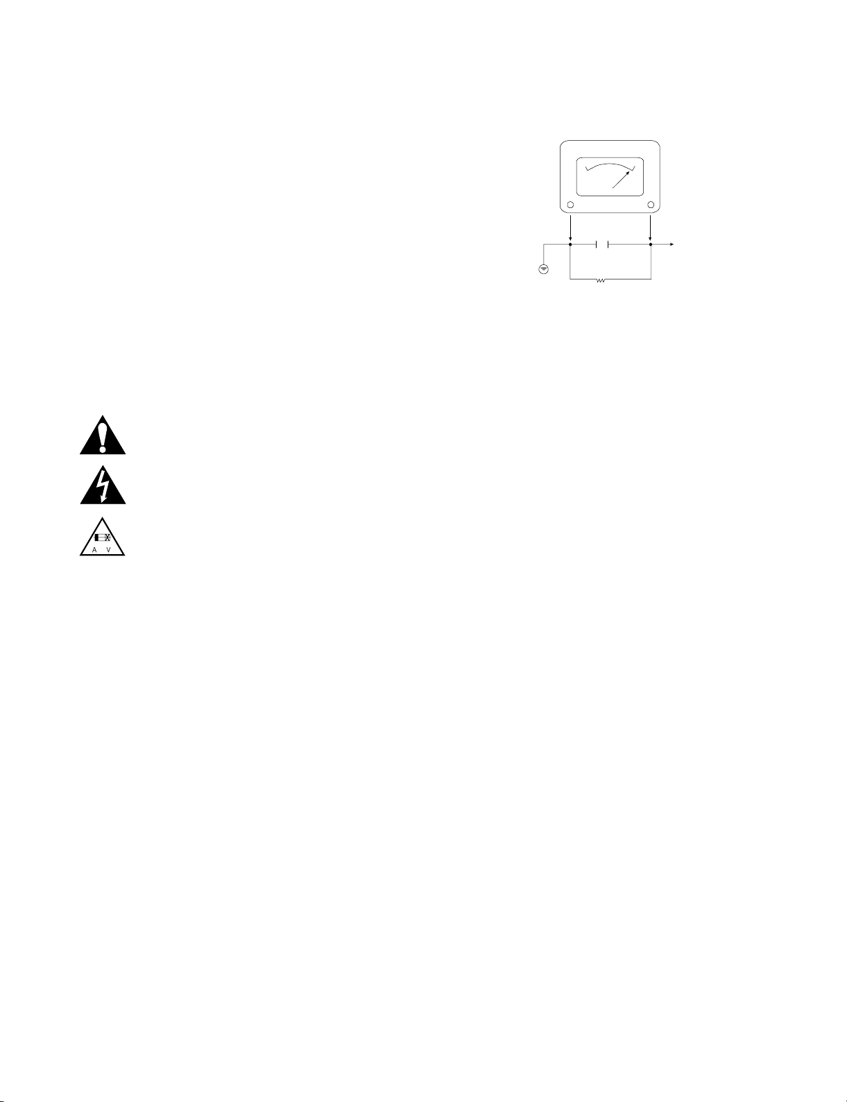
danger of electrical shock. DO NOT USE A LINE ISOLATION TRANSFORMER DURING THIS TEST. Use an AC voltmeter having 5000 ohms per
volt or more sensitivity in the following manner: Connect a 1500 ohm, 10
watt resistor, paralleled by a .15 mfd 150V AC type capacitor between a
known good earth ground water pipe, conduit, etc.) and the exposed metallic parts, one at a time. Measure the AC voltage across the combination of
1500 ohm resistor and .15 mfd capacitor. Reverse the AC plug by using a
non-polarized adaptor and repeat AC voltage measurements for each
exposed metallic part. Voltage measured must not exceed 0.75 volts RMS.
This corresponds to 0.5 milliamp AC. Any value exceeding this limit constitutes a potential shock hazard and must be corrected immediately.
TIPS ON PROPER INSTALLATION
1. Never install any receiver in a closed-in recess, cubbyhole, or closely fitting
shelf space over, or close to, a heat duct, or in the path of heated air flow.
2. Avoid conditions of high humidity such as: outdoor patio installations where
dew is a factor, near steam radiators where steam leakage is a factor, etc.
3. Avoid placement where draperies may obstruct venting. The customer
should also avoid the use of decorative scarves or other coverings that
might obstruct ventilation.
4. Wall- and shelf-mounted installations using a commercial mounting kit must
follow the factory-approved mounting instructions. A product mounted to a
shelf or platform must retain its original feet (or the equivalent thickness in
spacers) to provide adequate air flow across the bottom. Bolts or screws
used for fasteners must not touch any parts or wiring. Perform leakage tests
on customized installations.
5. Caution customers against mounting a product on a sloping shelf or in a tilted position, unless the receiver is properly secured.
6. A product on a roll-about cart should be stable in its mounting to the cart.
Caution the customer on the hazards of trying to roll a cart with small casters across thresholds or deep pile carpets.
7. Caution customers against using extension cords. Explain that a forest of
extensions, sprouting from a single outlet, can lead to disastrous consequences to home and family.
PRODUCT SAFETY SERVICING GUIDELINES FOR VIDEO PRODUCTS
A.C. Voltmeter
Good Earth Ground
such as the Water
Pipe, Conduit, etc.
0.15uF
1500 OHM
10 WATT
Place this probe
on each exposed
metal part.

1-3
SERVICING PRECAUTIONS
CAUTION: Before servicing the VCR + DVD RECODER covered by this service data and its supplements and addends,
read and follow the SAFETY PRECAUTIONS. NOTE: if
unforeseen circumstances create conflict between the following servicing precautions and any of the safety precautions in this publications, always follow the safety precautions.
Remember Safety First:
General Servicing Precautions
1. Always unplug the VCR + DVD RECODER AC power cord
from the AC power source before:
(1) Removing or reinstalling any component, circuit board,
module, or any other assembly.
(2) Disconnecting or reconnecting any internal electrical
plug or other electrical connection.
(3) Connecting a test substitute in parallel with an elec-
trolytic capacitor.
Caution: A wrong part substitution or incorrect
polarity installation of electrolytic capacitors may result
in an explosion hazard.
2. Do not spray chemicals on or near this VCR + DVD
RECODER or any of its assemblies.
3. Unless specified otherwise in this service data, clean
electrical contacts by applying an appropriate contact
cleaning solution to the contacts with a pipe cleaner,
cotton-tipped swab, or comparable soft applicator.
Unless specified otherwise in this service data, lubrication
of contacts is not required.
4. Do not defeat any plug/socket B+ voltage interlocks with
whitch instruments covered by this service manual might
be equipped.
5. Do not apply AC power to this VCR + DVD RECODER
and / or any of its electrical assemblies unless all solidstate device heat sinks are correctly installed.
6. Always connect the test instrument ground lead to an
appropriate ground before connecting the test instrument
positive lead. Always remove the test instrument ground
lead last.
Insulation Checking Procedure
Disconnect the attachment plug from the AC outlet and turn
the power on. Connect an insulation resistance meter (500V)
to the blades of the attachment plug. The insulation resistance between each blade of the attachment plug and accessible conductive parts (Note 1) should be more than 1Mohm.
Note 1: Accessible Conductive Parts include Metal panels,
Input terminals, Earphone jacks,etc.
Electrostatically Sensitive (ES) Devices
Some semiconductor (solid state) devices can be damaged
easily by static electricity. Such components commonly are
called Electrostatically Sensitive (ES) Devices. Examples of
typical ES devices are integrated circuits and some field
effect transistors and semiconductor chip components.
The following techniques should be used to help reduce the
incidence of component damage caused by static electricity.
1. Immediately before handling any semiconductor component or semiconductor-equipped assembly, drain off any
electrostatic charge on your body by touching a known
earth ground. Alternatively, obtain and wear a commercially available discharging wrist strap device, which
should be removed for potential shock reasons prior to
applying power to the unit under test.
2. After removing an electrical assembly equipped with ES
devices, place the assembly on a conductive surface such
as aluminum foil, to prevent electrostatic charge buildup or
exposure of the assembly.
3. Use only a grounded-tip soldering iron to solder or unsolder
ES devices.
4. Use only an anti-static solder removal device. Some
solder removal devices not classified as “anti-static” can
generate electrical charges sufficient to damage ES
devices.
5. Do not use freon-propelled chemicals. These can
generate an electrical charge sufficient to damage ES
devices.
6. Do not remove a replacement ES device from its protective package until immediately before you are ready to
install it. (Most replacement ES devices are packaged with
leads electrically shorted together by conductive foam,
aluminum foil,or comparable conductive material).
7. Immediately before removing the protective material from
the leads of a replacement ES device, touch the protective
material to the chassis or circuit assembly into which the
device will be installed.
Caution: Be sure no power is applied to the chassis or
circuit, and observe all other safety precautions.
8. Minimize bodily motions when handling unpackaged
replacement ES devices. (Normally harmless motion such
as the brushing together of your clothes fabric or the lifting
of your foot from a carpeted floor can generate static electricity sufficient to damage an ES device.)

1-4
SPECIFICATIONS
General
Power requirements AC 120V, 50/60 Hz
Power consumption 35W
Dimensions (approx.) 430 X 83.5 X 360 mm
Mass (approx.) 6.8 kg
Operating temperature 5 °C ~ 40 °C
Standard Condition -20 °C ~ -60 °C
Signal system NTSC
VDR PART
Read Disc Format DVD Disc : DVD Video Specification Book.
CD-DA Disc : RED Book.
Write Disc Format DVD-R/DVD-R/W Disc : DVD-RW Recorder Specification Book
Video System NTSC
Data Multiplexing MPEG-2(ISO/IEC 13818-1)
Data Decoding Standards MPEG-1, MPEG-2
Audio Compression Read : AC-3 : ATSC Standard for ATV MPEG-1, MPEG-2
Write : MPEG-1, Layer-2
VCR PART
Video Head System Double azimuth 4head helical scanning
Tape Format Tape width 12.7mm(0.5 inch)
Timer 24hours display type
OUTOUT
VIDEO OUTPUTS 1.0 V (p-p), 75 Ω negative sync,RCA jack x 1
S-VIDEO OUTPUT (Y)1.0 V (p-p), 75 Ω negative sync, Mini DIN 4-pin x 1
(C)0.3 V (p-p), 75 Ω
COMPONENT VIDEO OUTPUT (Y)1.0 V (p-p),75 Ω negative sync, RCA jack x 1
(Pb)/(Pr)0.7 V (p-p), 75 Ω
Audio output (analog output) (-)6dBm, less than 1kΩ RCA jack x 2
Audio output (digital output) 0.5 V (p-p), 75 Ω , RCA jack x 1
Audio output (optical output) 5 V (p-p), 75 Ω , Optical connector x 1

2-1
SECTION 2
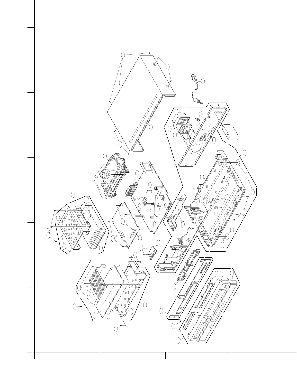
CABINET & MAIN CHASSIS
CONTENTS
EXPLODED VIEWS .....................................................................................................................2-2
1. Cabinet and Main Frame Section ...........................................................................................2-2
2. Packing Accessory Section....................................................................................................2-3
2-2
EXPLODED VIEWS
1. Cabinet and Main Frame Section
284
261
452
452
320
265
467
468
263
264
250
300
463
463
463
261A
261A
261A
283
280
A43
457
276
260
457
463
457
469
469
A50
A47
A48
A46
A00
457
TU701
323
A52
270
A26
A60
466
463
466
256
463
255
469
257
A47A
A44
452
A
5
4
3
2
1
BCD
2-3
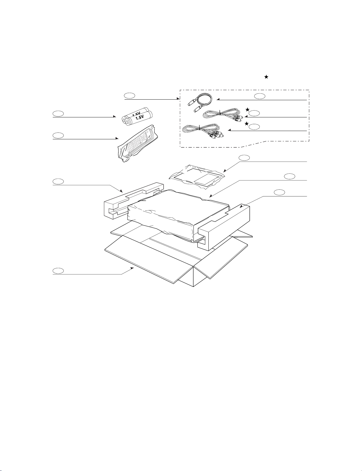
2. Packing Accessory Section
BATTERY
808
BAG
804
PACKING
803
806
INSTRUCTION ASSEMBLY
CABLE(COAXIAL)
810
CABLE ASS'Y RF
801
REMOCON
900
BOX CARTON
802
PACKING
803
811
812
PLUG ASS'Y 1WAY
PLUG ASS'Y 2WAY
OPTIONAL PARTS

3-13-1
SECTION 3
ELECTRICAL
CONTENTS
OVERALL WIRING DIAGRAM..............................3-2
VCR PART
ELECTRICAL ADJUSTMENT
PROCEDURES
............................................................3-3
VCR ELECTRICAL TROUBLESHOOTING
GUIDE
.............................................................................3-4
1. POWER(SMPS) CIRCUIT .......................................3-4
2. SYSTEM/KEY CIRCUIT ..........................................3-7
3. SERVO CIRCUIT ...................................................3--8
4. OSD CIRCUIT .......................................................3-10
5. Y/C CIRCUIT..........................................................3-11
6. TUNER/IF CIRCUIT...............................................3-15
7. Hi-Fi CIRCUIT........................................................3-17
BLOCK DIAGRAMS................................................3-20
1. POWER(SMPS) BLOCK DIAGRAM......................3-20
2. TUNER/MTZ BLOCK DIAGRAM...........................3-22
3. Y/C BLOCK DIAGRAM..........................................3-24
4. NORMAL AUDIO BLOCK DIAGRAM ....................3-26
5. JACK BLOCK DIAGRAM ......................................3-28
6. Hi-Fi BLOCK DIAGRAM ........................................3-30
7. SYSTEM BLOCK DIAGRAM.................................3-32
CIRCUIT DIAGRAMS..............................................3-34
1. POWER(SMPS) CIRCUIT DIAGRAM ...................3-34
2. TU/IF CIRCUIT DIAGRAM ....................................3-36
3. A/V CIRCUIT DIAGRAM........................................3-38
4. JACK CIRCUIT DIAGRAM ....................................3-40
5. Hi-Fi CIRCUIT DIAGRAM......................................3-42
6. SYSTEM CIRCUIT DIAGRAM...............................3-44
7. TIMER CIRCUIT DIAGRAM ..................................3-46
• WAVEFORMS .........................................................3-48
• CIRCUIT VOLTAGE CHART ...................................3-50
PRINTED CIRCUIT DIAGRAMS.........................3-52
1. VCR P.C.BOARD ...................................................3-52
2. POWER P.C.BOARD ............................................3-54
3. TIMER P.C.BOARD ..............................................3-54
4. KEY P.C.BOARD ..................................................3-56
5. JACK P.C.BOARD ................................................3-57
VDR PART
ELECTRICAL TROUBLESHOOTING
GUIDE & WAVEFORMS
........................................3-58
1. POWER(SMPS) CIRCUIT .....................................3-58
BLOCK DIAGRAMS................................................3-65
1. VDR MAIN H/ W BLOCK DIAGRAM.....................3-65
2. POWER BLOCK DIAGRAM ..................................3-66
3. AUDIO IN/ OUT BLOCK DIAGRAM......................3-67
4. CPU & CONTROL REGISTER
BLOCK DIAGRAM.................................................3-68
5. VIDEO IN/ OUT BLOCK DIAGRAM ......................3-69
CIRCUIT DIAGRAMS..............................................3-70
1. E5_BGA, POWER, UART2 CIRCUIT DIAGRAM..3-70
2. DDR_SDRAM, FLASH CIRCUIT DIAGRAM.........3-72
3. RST. CONTROL/STATUS_REG/ATAPI,
HOST_CPLD/LATCH CIRCUIT DIAGRAM ...........3-74
4. 1394, ETHERNET_CONNECTOR
CIRCUIT DIAGRAM ..............................................3-76
5. VIDEO_IN/OUT CIRCUIT DIAGRAM....................3-78
6. AUDIO IN/OUT, NON-STD_VIDEO
CIRCUIT DIAGRAM ..............................................3-80
7. AUDIO DAC, VIDEO_Y/MIXER
CIRCUIT DIAGRAM ..............................................3-82
8. FRONT A/V, 1934 JACK CIRCUIT DIAGRAM ......3-84
• WAVEFORMS .........................................................3-86
• CIRCUIT VOLTAGE CHART ...................................3-90
PRINTED CIRCUIT DIAGRAMS.........................3-94
1. VCR P.C.BOARD(TOP VIEW) ...............................3-94
2. POWER P.C.BOARD (BOTTOM VIEW)................3-96
RL-01A LOADER PART
ELECTRICAL TROUBLESHOOTING
GUIDE
...........................................................................3-98
BLOCK DIAGRAMS & DESCRIPTION ..........3-112
1. OVERALL BLOCK DIAGRAM .............................3-112
2. MAJOR IC INTERNAL BLOCK DIAGRAM AND
PIN DESCRIPTION .............................................3-113
3. MAJOR IC INTERNAL BLOCK DIAGRAM AND
PIN DESCRIPTION .............................................3-118
4. IC302(UPD76F0047):MICOM..............................3-127
WAVEFORMS ..........................................................3-131
1. POWER & RESET SIGNAL ................................3-131
2. MAIN CLOCK1 FOR IC202 (16.9MHZ)...............3-131
3. MAIN CLOCK2 FOR IC302 (20MHZ)..................3-132
4. SDRAM CLOCK ..................................................3-132
5. TRAY OPEN/CLOSE SIGNAL 1 ..........................3-133
6. TRAY OPEN/CLOSE SIGNAL 2 ..........................3-133
7. SLED MOVE SIGNAL 1.......................................3-134
8. SLED MOVE SIGNAL 2.......................................3-134
9. FOCUS SEARCH SIGNAL..................................3-135
10. LASER TURN ON SIGNAL ...............................3-135
11. DISC TYPE JUDGEMENT WAVEFORM
(CD SERIES) .....................................................3-136
12. DISC TYPE JUDGEMENT WAVEFORM
(CD&CD-R)........................................................3-136
13. DISC TYPE JUDGEMENT WAVEFORM
(CD-RW) ............................................................3-137
14. DISC TYPE JUDGEMENT WAVEFORM
(DVD SERIES)...................................................3-137
15. DISC TYPE JUDGEMENT WAVEFORM
(DVD_SINGLE&R).............................................3-138
16. DISC TYPE JUDGEMENT WAVEFORM
(DVD _DUAL) ....................................................3-138
17. DISC TYPE JUDGEMENT WAVEFORM
(DVDRW)...........................................................3-139
18. SPINDLE WAVEFORM1....................................3-139
19. SPINDLE WAVEFORM2....................................3-140
20. FOCUS ON SIGNAL(CD)..................................3-140
21. FOCUS ON SIGNAL(CD)..................................3-141
22. FOCUS ON SIGNAL(DVD)................................3-141
23. FOCUS ON SIGNAL (DVD)...............................3-142
24. TRACK OFF SIGNAL(CD).................................3-142
25. TRACK OFF SIGNAL(DVD) ..............................3-143
26. TILT DRIVER SIGNAL(DISC READING) ..........3-143
27. RF WAVEFORM(DVD) ......................................3-144
28. RF WAVEFORM(CD).........................................3-144
29. WOBBLE(DVD-R/RW)_READING ....................3-145
30. WOBBLE(DVD+R/RW)_READING&WRITING
=>X1 SPEED....................................................3-145
31. LD ENABLE(DVD) .............................................3-146
32. LD ENABLE(CD) ...............................................3-146
33. LASER POWER(READING)_DVD+RW............3-147
34. LASER POWER(ERASE)_DVD+RW ................3-147
35. LASER POWER(WRITING)_INITIAL STATE ....3-148
36. LASER POWER(WRITING)_PROCESSING ....3-148
CIRCUIT DIAGRAMS............................................3-149
1. RF CIRCUIT DIAGRAM .....................................3-149
2. DSP CIRCUIT DIAGRAM....................................3-151
3. µ-COM CIRCUIT DIAGRAM................................3-153
PRINTED CIRCUIT DIAGRAMS.......................3-155
1. MAIN P.C.BOARD(TOP SIDE) ............................3-155
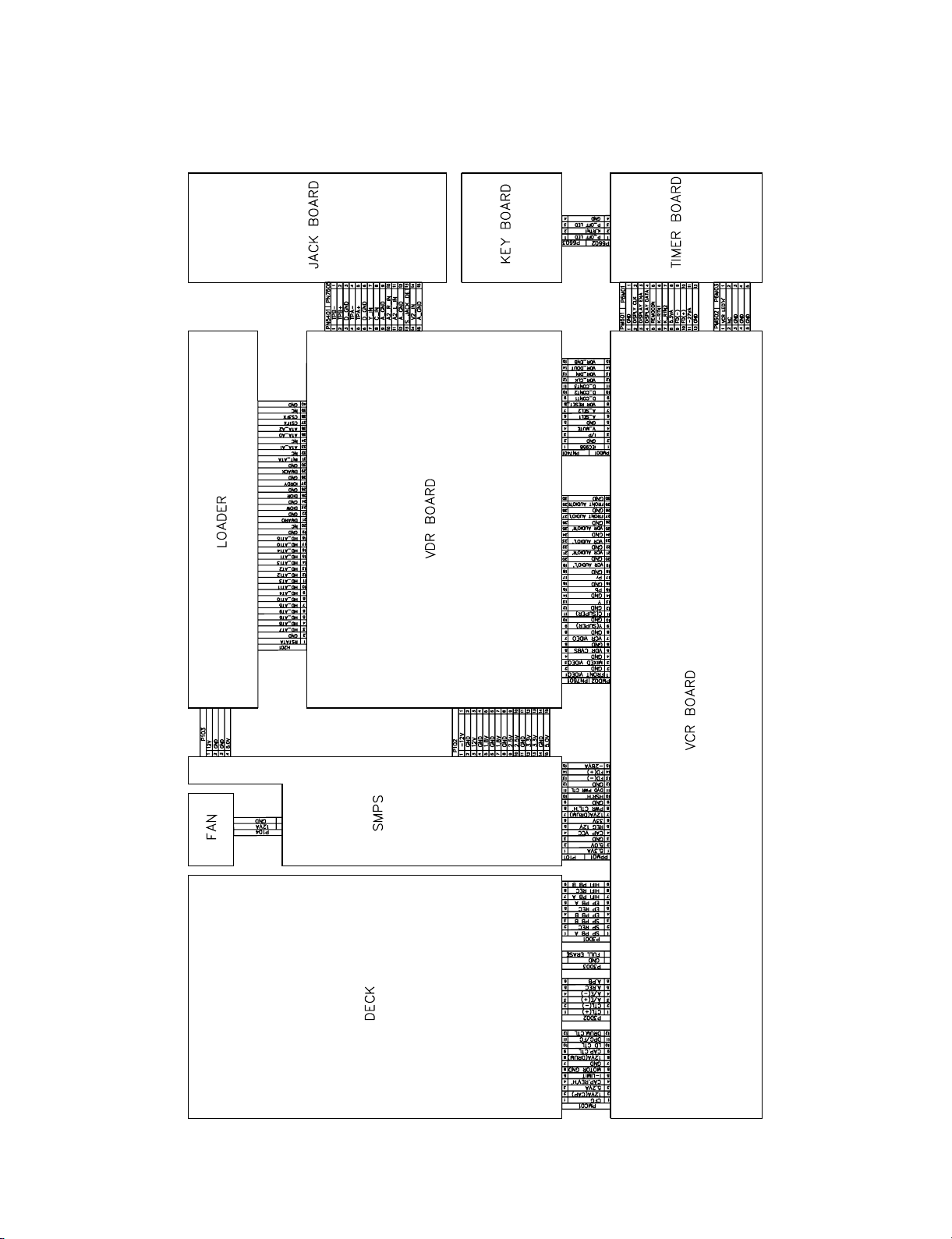
OVERALL WIRING DIAGRAM
3-2
3-3
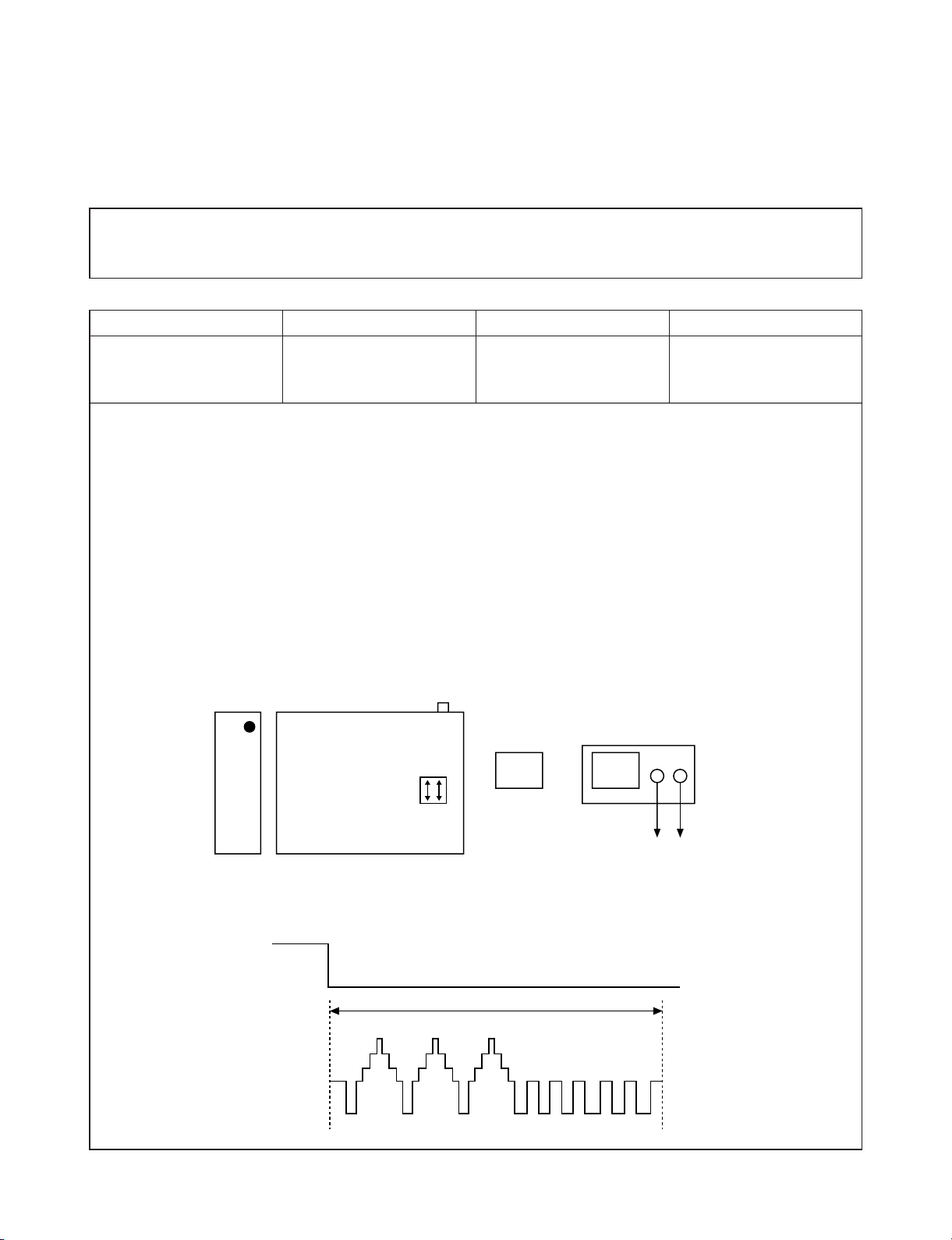
ELECTRICAL ADJUSTMENT PROCEDURES
1. Servo Adjustment
1) PG Adjustment
• Adjustment And Specification
• Test Equipment
a) OSCILLOSCOPE
b) NTSC MODEL : NTSC SP TEST TAPE
MODE
PLAY
• Adjustment Procedure
a) Insert the SP Test Tape and play.
b) Connect the CH1 of the oscilloscope to the H/SW and CH2 to the “VCR VIDEO” TP for the VCR.
c) Trigger the mixed Combo Video Signal of CH2 to the CH1 H/SW, and then check the distance (time dif-
ference), which is from the selected A(B) Head point of the H/SW(W5D1, W5D2) signal to the starting
point of the vertical synchronized signal, to 6.5H ± 0.5H (412µs, 1H=63.5µs).
• PG Adjustment Method
a-1) Playback the SP standard tape
b-2) Press the “ENTER” key on the Remote controller and the “REC” key on the Front Panel at the same
time, then it goes into Tracking initial mode. < Digitron[ - - ] >
c-3) Repeat the above step(No.b-2), then it finishes the PG adjusting automatically. < Digitron[ PG ] >
d-4) Stop the playback, then it goes out of PG adjusting mode after mony the PG data.
• CONNECTION
• WAVEFORM
V.Out
H/SW(W5D1, W5D2)
R/C TRK JIG KEY 6.5 ± 0.5H
MEASUREMENT POINT ADJUSTMENT POINT SPECIFICATION
H/SW
(W5D1, W5D2)
TP
(VCR
VIDEO)
(CH2)
(CH1)
OSCILLOSCOPE
CH1 CH2
R/C KEY
H/SW
(W5D1, W5D2)
VCR BOARDVDR BOARD
"VCR VIDEO" TP
VCR PART
H/SW
Composite
VIDEO
6.5H(412Ωs)

3-4
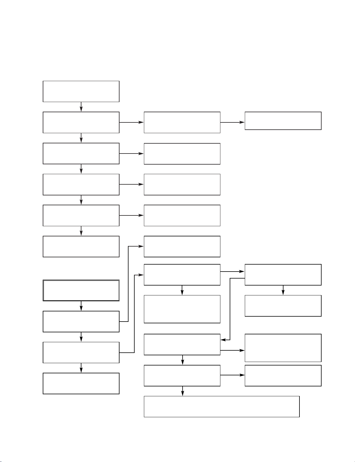
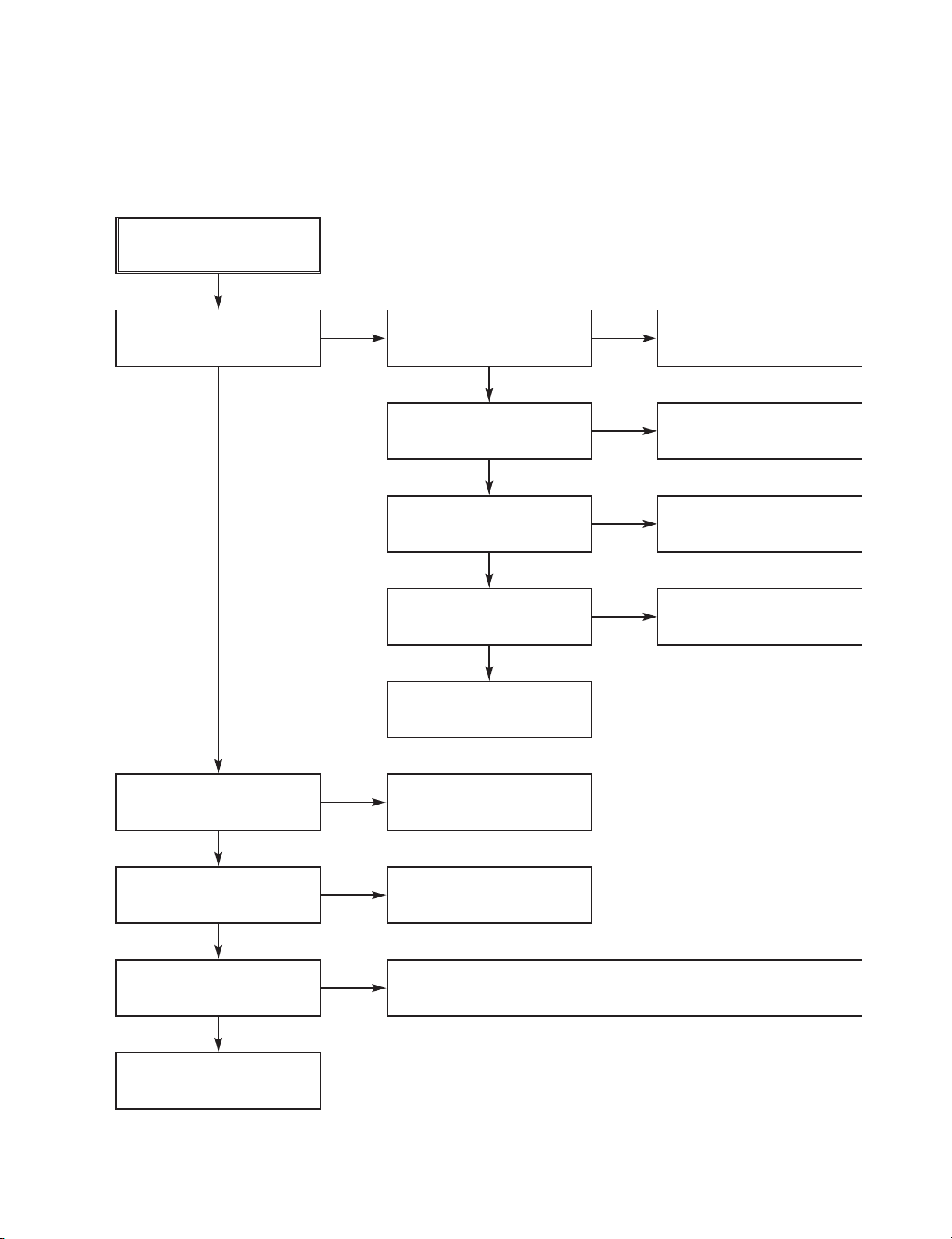
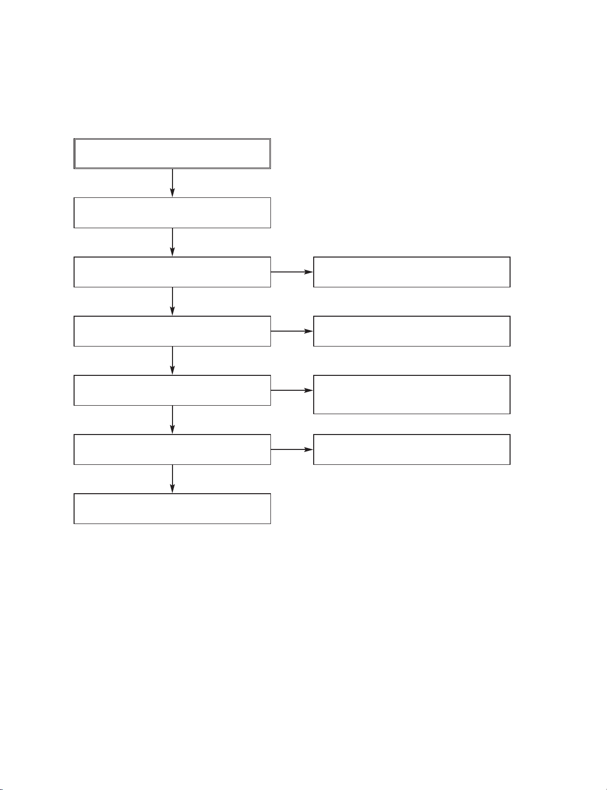
VCR ELECTRICAL TROUBLESHOOTING GUIDE
1. Power(SMPS) CIRCUIT
NO 5.3VA.
Replace the F101
(Use the same Fuse)
Is the F101 normal?
Is the TH01
Normal?
Is the BD101
Normal?
NO
NO
NO
NO
NO
NO
NO
NO
NO
NO
NO
Replace the BD101
Replace the TH01
Is the D102
normal?
Check or Replace
the D102
Replace the D121
Replace the IC103
Replace the D126
Replace the D129
Replace the D130
Replace the D127
Replace the D128
YES
YES
YES
YES
YES
YES
YES
YES
YES
YES
Is the Vcc (11V - 18V)
supplied to IC101 Pin2?
NO
Is the D121
normal?
Is there about 2.5V
at the IC103 Pin1?
Is the D126
normal?
Is the D129
normal?
Is the D130
normal?
Is the D127
normal?
Is the D128
normal?
YES
Power Line of Main
PCB(VCR) is short
VCR ELECTRICAL TROUBLESHOOTING GUIDE
3-5
No 12VA
Check or Replace
the D126
Is the Vcc(13V)
supplied to C130?
Check or Replace
the Cap / Drum
Is the D132
Normal?
NO
NO
Replace the D132
YES
YES
(To Cap, Drum Motor )
No REG 12V
Check or Replace
the D126
Check the ‘PWR CTL
“H”’signal from µ-com
Check the 33V Line
Replace the Q126
Is the Vcc(13V) supplied to Q126Collector?
Is the Vcc(33V) supplied to Q126 Base?
Is the Q126 Nomal?
Check or Replace
the D126
NO
NO
NO
YES
YES
YES
NO VFD
Check or Replace
the R107
Is the R107
Normal?
Is the D128
Normal?
NO
Check or Replace
the D128
Check or Replace
the ZD151
NO
NO
YES
Is the ZD151
Normal?
Check or Replace
the D127
YES
YES
No 33V
Check or Replace
the D130
Is the Vcc(33V) supplied to Q123 Emittor?
Is the Q123 Base
‘H’?
NO
Check the ‘PWR CTL
“H”’signal from µ-com
NO
YES
Check or Replace
the Q123
YES

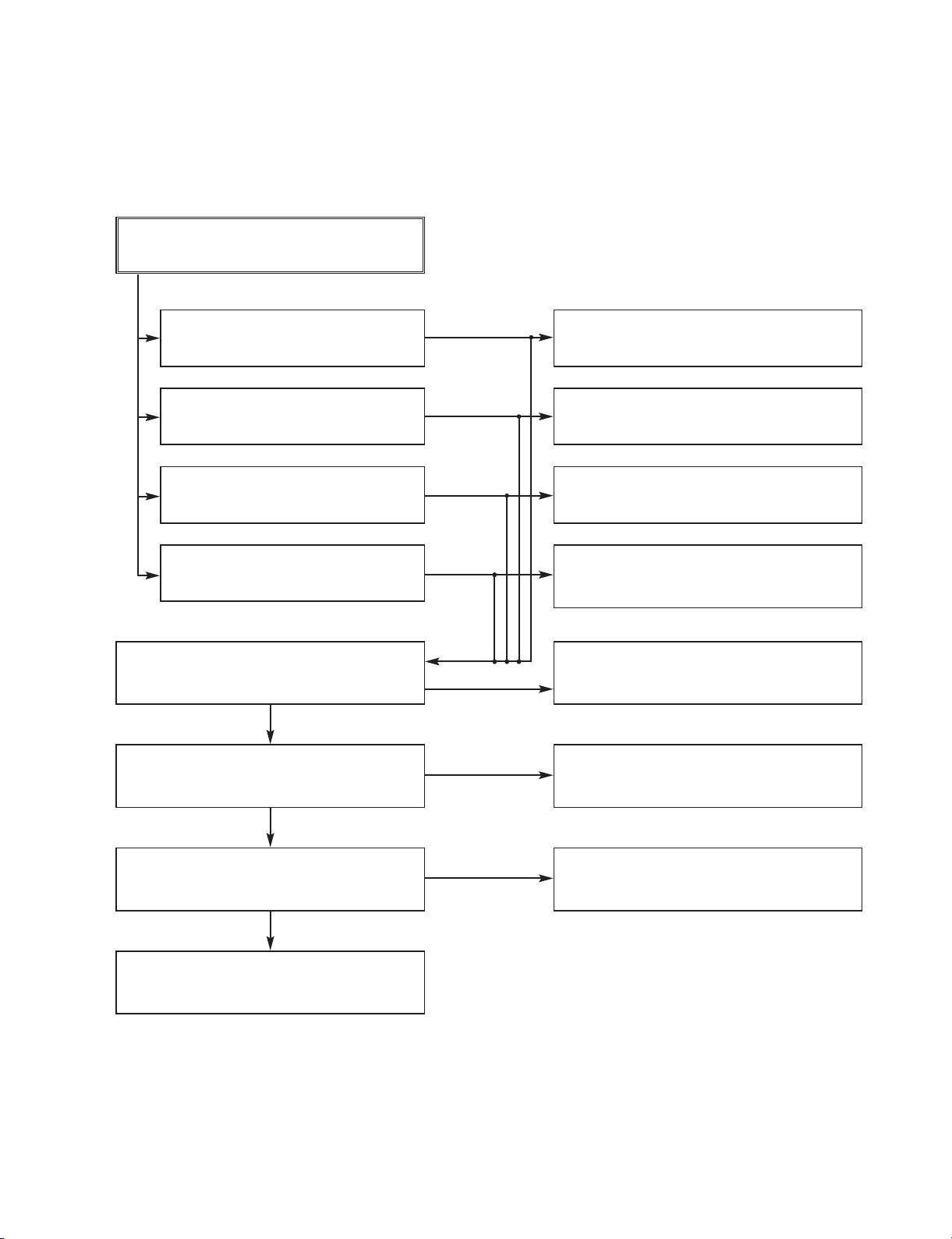
3-6
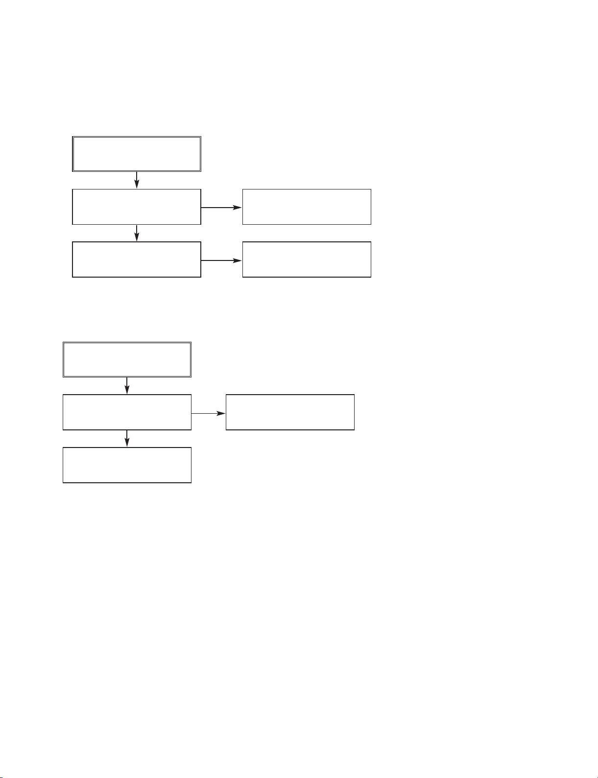
VCR ELECTRICAL TROUBLESHOOTING GUIDE
No 28V (HSR)
Check or Replace
the D129
Is the Vcc(30V) supplied
to Q120 Collector?
Is the Vcc(33V) supplied
to Q121 Collector?
Is the Vcc(30V) supplied to Q120 Base?
NO
NO
Check or Replace
the ZD153
NO
Check the ‘HSR “H”
signal from µ-com
Check or Replace the
Q121/Q122 & 33V line
YES
YES
Check or Replace
the Q120
YES
3-7
2. SYSTEM/KEY CIRCUIT
(1) AUTO STOP
(2) The unstable loading of a Cassette tape
Auto Stop
Does the SW30 waveform
appear at IC501 Pin18?
Do the T-UP Reel Pulses
appear at IC501 Pin80?
Is 12V applied to PMC01
Pin8?
Check the Drum Motor
signal.
Does 5V appear at the
RS501?
Check the Q124 Power
Circuit.
Refer to “SMPS DRUM
12 Volt Trouble Shooting”.
Is 5V applied to R531 ?
Refer to SMPS 5.3VA
troubleshooting.
Check IC501
Pins22, 23, 24, 25.
Do T/UP Reel Pulses
appear at the point
between R556 and R536?
Replace the T/UP Reel
Sensor (RS501).
Check the CST SW and
the peripheral circuitry.
Replace the IC501.
The unstable loading of a
Cassette tape
Does the “H” signal appear
at IC501 Pin60 while
inserting the CST ?
Does the “L” signal appear
at IC501 Pin19 while
inserting the CST?
Check the Deck
Mechanism.
Note :
Auto stop can occur because Grease or Oil has dried up
YES
YES
NO
YES
YES
YES
NO
NO
NO
NO
NO
NO NO
YES
YES YES
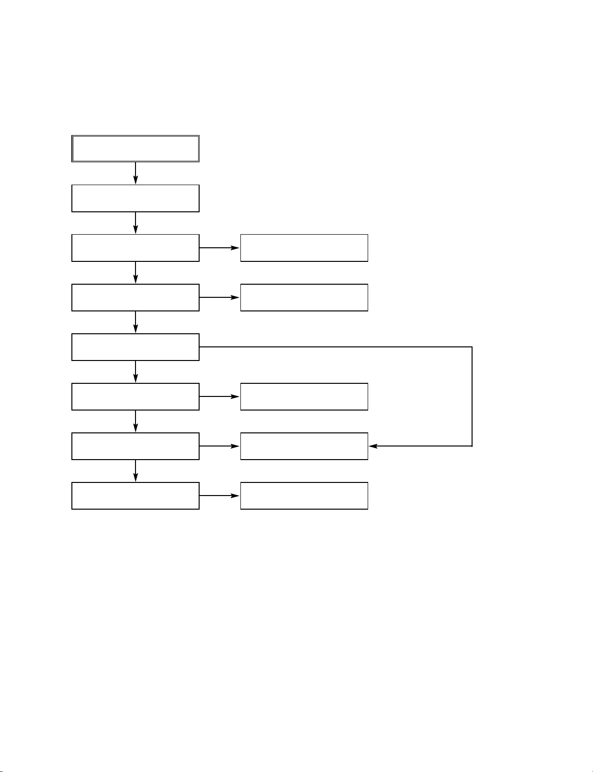
VCR ELECTRICAL TROUBLESHOOTING GUIDE
3-8
3. SERVO CIRCUIT
(1) Unstable Video in PB MODE
Does the Noise level of the
screen change
periodically?
Do the CTL pulses appear
at IC501 Pin97?
Is the height adjustment of
the CTL Head accurate?
Check Deck Motor.
Readjust the height of the
CTL Head.
Replace IC501.
Refer to “When the Y signal
doesn’t appear on the
screen in PB Mode”.
Confirm the CFG
waveform at IC501 Pin87?
On tracking, do the CTL
pulses move?
Does the Video Envelope
waveform appear at IC501
Pin9?
Replace IC501.
YES
YES
YES
NO NO
NO
NO
NO
(2) When the Drum Motor
(2) doesn’t run.
Do the DFG Pulses appear
at PMC01 Pin11?
Replace the Cap M.
Are the foil patterns and
the Components between
IC501 Pin 90 and PMC01
Pin11 shorted?
Replace IC501.
Refer to “(2)
No 12VA of Power section”
Do the Drum PWM Pulses
appear at IC501 Pin76?
Are the foil patterns and
the Components between
IC501 Pin76 and PMC01
Pin12 shorted?
Do the DFG Pulses appear
at IC501 Pin90?
Do the Drum PWM Pulses
appear at IC501 Pin76?
Are the connecting patterns and the Components
between IC501 Pin76 and PMC01 Pin12 shorted?
When the Drum Motor
doesn’t run,
Does 12V appear at
PMC01 Pin8?
Does 2.8V appear at
PMC01 Pin12?
Check the connector
(PMC01) and the Drum
Motor Ass’y.
NO
YES
YES
YES
NO
NO
NO
NO
NO
YES
YES
YES
VCR ELECTRICAL TROUBLESHOOTING GUIDE

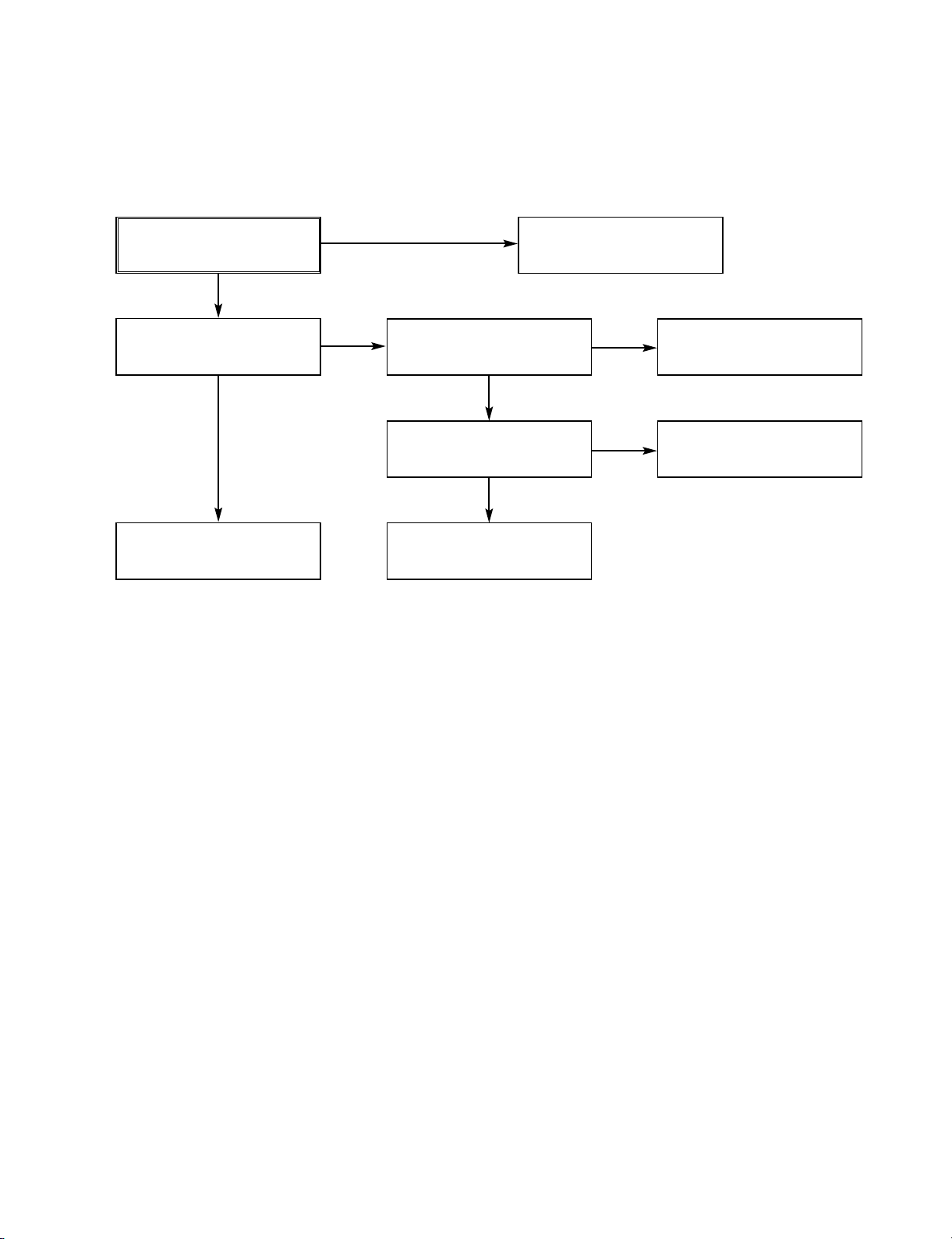
3-9
Does the CFG signal appear at
PMC01 Pin1?
Does the PWM signal appear at IC501
Pin77?
Does 2.8V appear at PMC01?
Check the PMC01 and the Capstan
Motor Ass’y.
Does the Capstan PWM signal appear at
IC501 Pin77?
Are the foil patterns and Components
between IC501 Pin77 and PMC01
Pin9 shorted?
Does the CFG signal come into IC501
Pin87?
Are the foil patterns and Components
between IC501 Pin77 and PMC01
Pin9 shorted?
2. SERVO CIRCUIT
(3) When the Capstan Motor doesn’t run,
NO
NO
NO
YES
YES
YES
When the Capstan Motor doesn’t run,
Does 12VA appear at PMC01?
YES
Replace IC501.
YES
NO
NO
YES
Refer to “SMPS(CAPSTAN/12Volt)
Trouble Shooting”.
Are the foil patterns and component
between IC501 Pin87 and PMC01
Pin1 shorted?
Check the Capstan Motor Ass’y.
NO
VCR ELECTRICAL TROUBLESHOOTING GUIDE
3-10
4. OSD CIRCUIT
(1) I
2
C BUS CHECK
Keys do not work
Is 5V applied to IC501
Pin78?
Does FLD change when
a function button is
pressed?
No I2C bus communication
Does Power appear at the
Pull up impedence
(R569, R507)?
Replace IC501.
Refer to “SMPS 5.3VA
Trouble Shooting”.
Replace the defective
switches.
Refer to “SMPS 5.3VA
Trouble Shooting”.
YES
YES
NO
NO
NO
2. SERVO CIRCUIT
(4) Keys do not work
VCR ELECTRICAL TROUBLESHOOTING GUIDE

3-11
5. Y/C CIRCUIT
(1) No Video in EE Mode,
No Video in EE Mode
Does the Video signal
appear at IC301
Pins28, 30, 32?
Is REG 5.0V applied to
IC301Pins23, 44, 45, 52, 68,
77?
Does the Video signal
appear at IC301 Pin26?
Does the Video signal
appear at IC501 Pin52?
Does the Video signal
appear at PMD02 Pin7?
Does the Video signal
appear at the PMD02
Pin5?
Does the Video signal
appear at the JK602
Video Out Jack?
Check the REG 5V Line.
(Power Circuit)
Is I2C BUS signal applied to
IC301 Pins53, 54, 55?
Replace IC301.
Check the path of the signal between IC301 Pin 26
and IC501 Pins50, 52.
Is there REG12 on the
plus terminal of C653?
Check the REG 12V Line.
(Power Circuit)
Check the Q605
(Video Buffer)
Check the VDR
Module
Check the IC601 and
Video Out Line
Check the System Circuit.
(Refer to ‘SYSTEM I2C BUS
CHECK Trouble Shooting’)
YES
YES
YES
YES
YES
YES
YES
YES
NO
NO
NO
NO
NO
NO
NO
NO
Check the REG 5V Line.
(Power Circuit)
NO
NO
Check VDR Video Input
(PMD02 Pin 5), Tuner Video
Input (TU701 Pin24), Line
Video Input (IC602 Pins 1, 3,
5, 7), respectively.
VCR ELECTRICAL TROUBLESHOOTING GUIDE
3-12
3. Y/C CIRCUIT
(2) When the Y(Luminance) signal doesn’t appear on the screen in PB Mode,
Is 5V applied to IC301
Pins23, 44, 45, 52, 68, 77?
Is the Y/C Bus siganl
applied to IC301 Pins53,
54, 55?
Does the normal RF signal
appear at IC301 Pin14?
Check the line of the REG
5V Line. (Power Circuit)
Check the System Circuit.
(IC501 Pin18)
Check the V.H.S/W level.
Refer to ‘SYSTEM Y/C
BUS CHECK Trouble
Shooting’.
Is the V.H.S/W signal
applied to IC301 Pin57?
Does the Rectangular
waveform(5V) appear at
IC301 Pin57(V.H.S/W)
Clean the Drum.
Check C324.
Check R328, C322, C323.
Does the Y(Luminance)
signal appear at IC301
Pin20?
Is the Y(Luminance) Video
waveform showed up at
IC301 Pin22?
Replace IC301.
NO
YES
YES
YES
YES
YES
YES
YES
NO
NO
NO
NO
NO
NO
VCR ELECTRICAL TROUBLESHOOTING GUIDE
3-13
3. Y/C CIRCUIT
(3) When the C(Color) signal doesn’t appear on the screen in PB Mode,
Is 5V applied to IC301
Pins23, 44, 45, 52, 68, 77?
Does the Color signal
appear at IC301
Pins41, 50?
Check the line of the REG
5V Line. (Power Circuit)
Replace X301.
Check C342, C341,
R333.
Is X301 (3.58MHz)
normal?
Replace IC301.
Does the Color signal
appear at IC301 Pin48?
Replace IC301.
NO
YES
YES
YES
NO
NO
NO
VCR ELECTRICAL TROUBLESHOOTING GUIDE

3-14
3. Y/C CIRCUIT
(4) When the Video signal doesn’t appear on the screen in REC Mode,
YES
YES
NO
NO
YES
YES
YES
YES
YES
Check system part
(V.H/SW)
Replace the IC301.
Check the drum
*OPTION
Pins72, 73, 74(SP)
Pins65, 66, 67(EP)
REC mode
Check the EE mode
NO
Is EE mode normal?
Is color
normal?
A
A
YES YES
Is brightness normal?
Does signal appear at
IC301 Pins41, 50?
NO
Check X301 oscillation
frequency.
YES
Is the brightness signal supplied to IC301 Pins18?
Is 5V supplied to IC301
Pins23, 44, 45, 68, 77?
Check the power of Pins23,
44, 45, 52, 68, 77.
Check the 5V power
NO
NO
NO
NO
NO
Is Y/C Bus applied to
IC301 Pins53, 54, 55?
Check the REG 5V power
Check system part
Do X301 and X-TAL
oscillate?
Check X301
Is V.H SW supplied to
IC301 Pin57?
Does the FM signal appear
at IC301*?
VCR ELECTRICAL TROUBLESHOOTING GUIDE
3-15
6. Tuner/IF CIRCUIT
(1) No Picture on the TV screen
No picture on the TV
screen
Does the Video signal
appear at TU701 Pin16.
YES YES
Is +33V applied to TU701
Pin14?
YES
Is +5V applied to TU701
Pin3?
NO
Does the video signal
appear at IC302 Pin7.
NO
Does the Video signal
appear at IC501 Pin 52.
YES
NO
Does the Video signal
appear at IC602 Pin 7.
YES
NO
Check the signal flow from IC602
Pin7 to JK601 Pin Video out.
YES
Check 33V line.
NO
Check 5V line.
NO
YES
Does the Clock signal
appear at TU701 Pin9?
Check the l2C Clock Signal
of µ-COM Pin71.
NO
YES
Does the data signal
appear at TU701 Pin10?
Replace Tuner.
Check the signal flow from
IC501 Pin27.(Pin27 is ‘L’
state in Tuner Mode)
Check the signal from IC301
Pin26 to IC501 Pin50.
Check the signal from IC501 Pin52 to IC602 Pin1 and IC602 Pin2.
(IC602 Pin2 is ‘L’ state in VHS mode)
Check the l2C Data Signal
of µ-COM Pin72.
NO
VCR ELECTRICAL TROUBLESHOOTING GUIDE
3-16
VCR ELECTRICAL TROUBLESHOOTING GUIDE
(B) No Sound
No Sound.
Check the Vcc of IC701 Pins1, 11, 19,
22, 33.
YES
Check 5.2V Line.
NO
Check the Tuner SiF signal at IC701
Pin2.
YES
Check the oscillator of IC701 Pins5, 6.
YES
Check the Audio of IC701 Pins30, 31.
YES
Check the Audio of IC801 Pins2, 3.
YES
Check the Audio of IC801 Pins16, 17.
YES
Check the Tuner SIF of TU701 Pin22.
NO
Replace X751
NO
Check the IIC Clock and Data at IC701
Pins12, 13.
NO
Check the signal flow from IC701
Pins30, 31 to IC801 Pins2, 3.
NO
Check the IIC Clock and Data at IC801
Pins42, 43.
NO
3-17
VCR ELECTRICAL TROUBLESHOOTING GUIDE
7. Hi-Fi CIRCUIT
(1) No Sound(EE Mode)
YES
No Sound.
Check the TU Audio of IC801
Pins2, 3.
Check the DVD Audio of IC801
Pins4, 5.
Check the AV1 Audio of IC801
Pins6, 7.
Check the AV2 Audio of IC801
Pins8, 9.
Check the Vcc of IC801 Pins34, 40,
IC802 Pin4.
YES
Check the IIC Clock and DATA at
IC801 Pins42, 43
YES
Check the Audio of IC801 Pins16, 17.
YES
Check the JK601.
Check the IC701 Pins30, 31.
NO
Check the VDR MODULE.
(PMD02 Pins23, 25).
NO
NO
Check the RCA Jack.
(JK601 Scart1 Audio in L, R).
NO
Check the VDR MODULE.
(PMD02 Pins27, 29).
Check the Power 5.2V, 12V.
YES
NO
Check the IC501 Pins71, 72.
NO
Replace IC801.
NO
3-18
VCR ELECTRICAL TROUBLESHOOTING GUIDE
3. Y/C CIRCUIT
(2) Hi-Fi Playback
YES
YES
YES
YES
PB mode
No Sound.
Check the Vcc of IC801
(Pins34, 40)
Check the Hi-Fi Selection switch.
(IC801 Pin41) and the Tape quality.
Is the RF Envelope at
IC801 Pin44 over 2Vp-p?
YES
Check IC801 Pin42(Data),
Pin43(Clock)
YES
Do Audio Signals appear at
IC801 Pin16(L-CH), 17(R-CH)?
YES
Do Audio Signals appear at
JK601?
Check Power 5.2V, 12V.
NO
Check IC501 Pin19
(A.H/SW)
NO
NO
Check the parts of µ-COM
(IC501 Pins71, 72)
NO
Check the Connection at
P3D01 Pins7, 9.
NO
Check the Jack(JK601)
NO
3-19
(3)
Hi-Fi REC.
It can’t be recorded Hi-Fi Audio
signal.
Check Vcc of IC801.(Pins34, 40)
YES
YES
Check IC801 Pin42(Data), Pin43(CLOCK).
YES
Do Audio signals appear at IC801
Pins16, 17?
YES
Do FM Audio signals appear at IC801
Pin36?
YES
Check the Contact Point of Drum
Connector if good then Replace the Drum.
YES
Check Power 5V, 12V.
NO
Check ports of µ-COM.
(IC501 pins 71, 72)
Check Audio input signal of IC801
Pins2, 3(TU.A.), 4, 5(AV1), 6, 7(VDR.A.),
10, 11(AV2).
NO
Replace IC801.
NO
NO
VCR ELECTRICAL TROUBLESHOOTING GUIDE
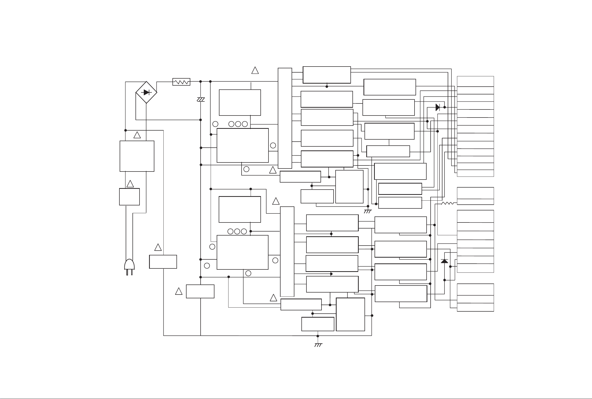
FUSE
(F101)
NOISE FILTER
BLOCK
(C101,L102,
L101, C102)
SNUBBER
BLOCK
(D103,C115,C116
,R112,R115)
DRIVE & S/W BLOCK
(IC104, D104, R113,
C117,C114)
BD101
TH01
Y-CAP
C110
Y-CAP
C111
+
BR BL
(BK)(WH)
2.5V
3.3V
TO VDR
(P102)
C103
12V
5.0V
TO LOADER
(P103)
FD( +)
FD(-)
-28VA
TO VCR
(P101)
!
!
!
!
5.3VA
5.0V
Cap Vcc
12VA( DRUM)
33V
REG 12V
PWR CTL 'H'
HSR 'H'
DVD PWR CTL
5.0V
SNUBBER
BLOCK
(D101,C105
C106,R103)
DRIVE & S/W BLOCK
(IC101, D102, R105,
C108,C112)
T101
T102
!
!
PHOTO COUPLER
(IC102)
ERROR AMP
(IC103)
FEED-BACK
BLOCK
R121,R122,
C121,R123.
R124.R125
R126)
!
RECTIFIER &
SMOOTING BLOCK
(D128,C133,R130)
RECTIFIER &
SMOOTING BLOCK
(D127,C131,L125,C132)
RECTIFIER &
SMOOTING BLOCK
(D125,C139,L127,C140)
RECTIFIER &
SMOOTING BLOCK
(D124,C129)
RECTIFIER &
SMOOTING BLOCK
(D123,C126,L124,C127)
RECTIFIER &
SMOOTING BLOCK
(D122,C123,L123,C125)
PHOTO COUPLER
(IC105)
ERROR AMP
(IC106)
FEED-BACK
BLOCK
R131,R132,
C141,R133.
R161.R162
R163)
!
12V REG & S/W Block
(IC157,R156,C155)
-12V
12V
1.8V
8.7V
TO FAN
(P103)
RECTIFIER &
SMOOTING BLOCK
(D129,C128,R147)
RECTIFIER &
SMOOTING BLOCK
(D130,C137,R146)
5.0V REG & S/W Block
(IC151,R151,C151)
1.8V REG & S/W Block
(IC160,R159,C152)
3.3V REG & S/W Block
(IC154,R154,C154)
RECTIFIER &
SMOOTING BLOCK
(D126,C136,L122,C130)
RECTIFIER &
SMOOTING BLOCK
(D121,C122,L121,C124)
HSR S/W Block
(Q120,ZD153,C135,
R144,R145,D155,C157)
12V REG & S/W Block
(Q126,R150,ZD152,
C156,C153)
5.0V S/W Block
(Q124,R140,R135,R136
D134,C134)
33V S/W Block
(Q123,R143,R134)
HSR CTL Block
(Q121,Q122,R141)
PWR CTL Block
(Q125,R137,R138)
5 6 7 8
5
1
2
3
6 7 8
2
3
3-20 3-21
BLOCK DIAGRAMS
1. POWER(SMPS) BLOCK DIAGRAM
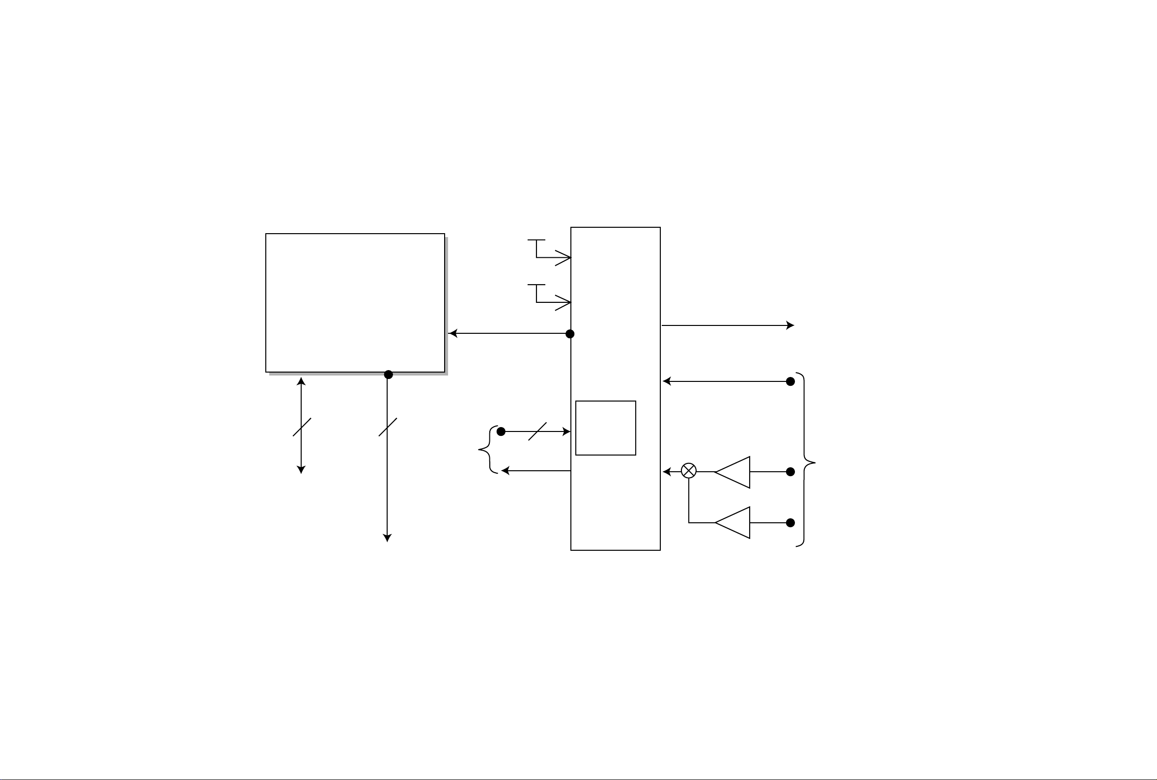
TU701
TUNER
FROM/TO
MICOM
(IC501)
1. TO JACK PART
(IC603, NJM2750)
2. TO Hi-Fi IC
(IC801)
FROM/TO
MICOM
(IC501)
SIF
33V
(PMP01-6)
5.0V
(PMP01-2)
CH S/W
IIC CLK
IIC DATA
VCR'H'
TO
AVCP IC
(IC301)
FROM
JACK
PART
TU.V.OUT
V.IN
A.IN
Q702
Q703
VDR A.L
VDR A.R
AFT
IC701
MSP3407
IIC CLK
IIC DATA
TU.A.L
TU.A.R
3-22 3-23
2. TUNER/MTZ BLOCK DIAGRAM
3-24 3-25
3. Y/C BLOCK DIAGRAM
EP PB 'A'
EP PB 'B'
SP PB 'B'
SP PB 'A'
64
59 58 57 55 54 53
65
67
72
74
ACC
DET
ENV
DET
C-ROT
RF-SW
IN
Y/C ENA
Y/C DATA
Y/C CLOCK
V.OUT
AUDIO
MUTE
HA SW
P
P
P
C-LPF
MAIN
CONV
3.58M
BPF2
ACC
AMP
ACC
DET
CLAMP
Y
LPF
CLAMP
CLAMP
IN
OUT
VCA
CCD
3.58M
BPF1
Y/C
MIX
6dB
DOUBLE
LIMFMDEM
SUB
LPF
MAIN
DE-EM
PB
FM-EQ
FM
AGC
CNC
YNR
COMB
4.21M
BPF
SUB
CONV
39
37
36
34
26
22
21
P
B
(PB Mode)
EP REC
SP REC
57
V. H/SW55Y/C ENA
54
Y/C DATA
53 51 50 49 48 47
39
38
37
36
34
32
30
28
22
21
20
73
70
69
66
Y/C CLOCK
X-TAL
3.58MHZ
C-LPF
MAIN
CONV
4.21M
BPF
SUB
CONV
DETAIL
ENH
MAIN
EMPHA
REC
FM-EQ
4.7K
FM
MOD
Y
LPF
YNR
COMB
3.58M
BPF1
LINE2
26
V.OUT
DVD
TU/LINE1
VIDEO
AGC
CLAMP
CLAMP
CLAMP
IN
CCD
OUT
VCA
SW
BLOCK
IC302
NL
EMPHA
B-UP
AMP
ACC
AMP
ACC
DET
BGA
REC
APC
REC
APC
320FH
VCO
SLDVX01
SERIAL
DECODER
R
R
B
(REC Mode)
 Loading...