

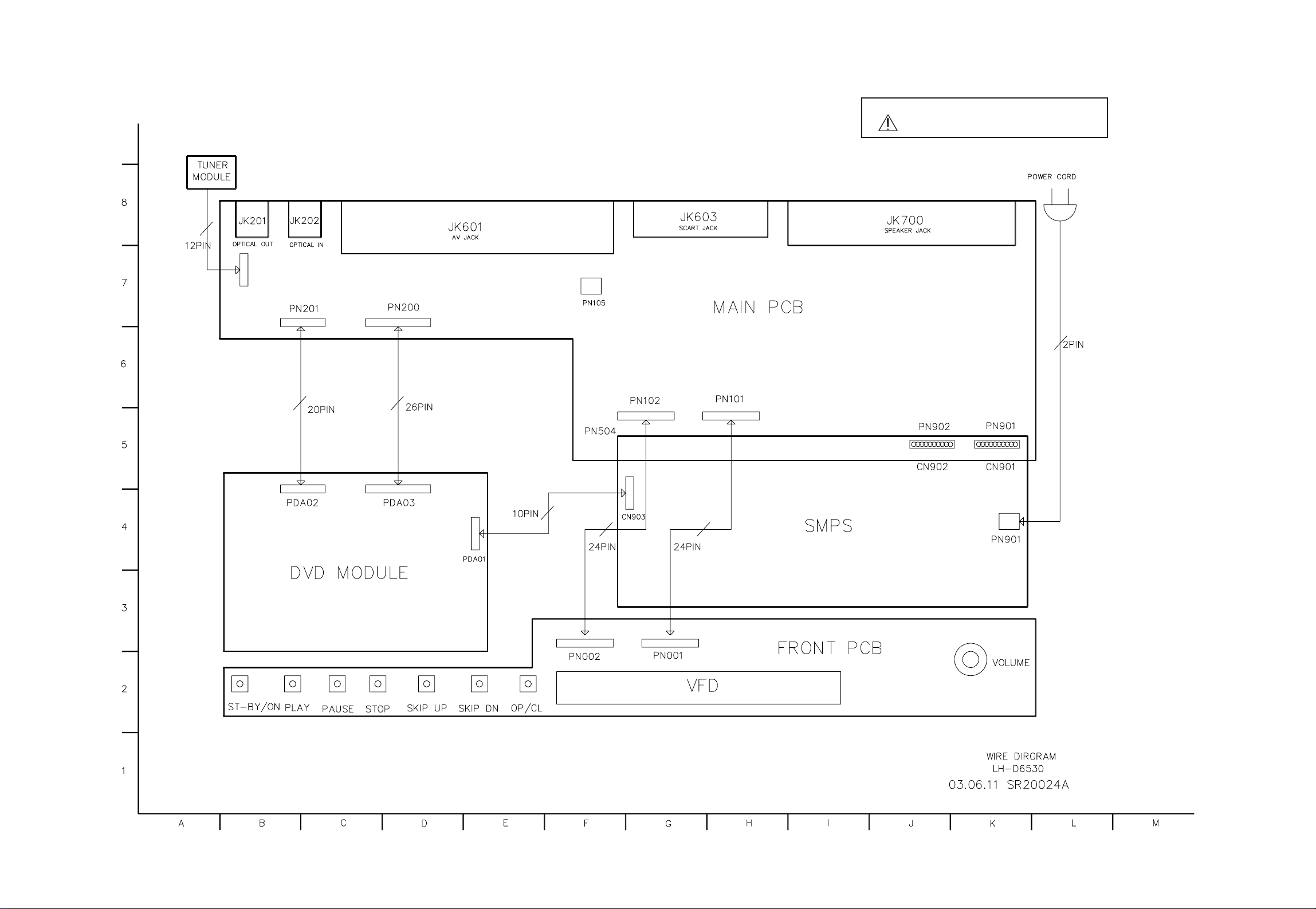
Page 1
SERVICE MANUAL MODEL: LH-DW6530 FE-6100CVE, FE-6100TE, FE-6100WE FA-W6100SL, FA-W6100SR, ACC-W6100
CD-R/RW
DVD/CD RECEIVER
SERVICE MANUAL
P/N : 3829RAT091D SEPTEMBER, 2003
MODEL:LGHTW316
FE-6100CVE, FE-6100TE, FE-6100WE
FA-W6100SL, FA-W6100SR, ACC-W6100
Page 2
- 1-1 -
SECTION 1. GENERAL
• SERVICING PRECAUTIONS
.......................................................................................................
1-2
• ESD PRECAUTIONS
...................................................................................................................
1-4
• SPECIFICATIONS
........................................................................................................................
1-5
• LOCATION OF CUSTOMER CONTROLS
...................................................................................
1-6
SECTION 2. AUDIO PART
• ELECTRICAL TROUBLESHOOTINGGUIDE............................................................................... 2-1
• BLOCK DIAGRAM
........................................................................................................................
2-6
• SCHEMATIC DIAGRAMS
............................................................................................................
2-8
• WIRING DIAGRAM
....................................................................................................................
2-20
• VOLTAGE SHEET (IC&TR) ........................................................................................................ 2-22
• PRINTED CIRCUIT DIARGAMS
................................................................................................
2-26
SECTION 3. DVD PART
• ELECTRICAL TROUBLESHOOTING GUIDE
.............................................................................
3-1
• DETAILS AND WAVEFORMS ON SYSTEM TEST AND DEBUGGING ...................................... 3-8
• DVD PART SCHEMATIC DIAGRAMS
........................................................................................
3-21
• VOLTAGE SHEET (IC & TR)
......................................................................................................
3-27
• PRINTED CIRCUIT DIAGRAM
...................................................................................................
3-29
SECTION 4. EXPLODED VIEWS
......................................................................................
4-1
SECTION 5. REPLACEMENT PARTS LIST
.....................................................................
5-1
SECTION 6. SPEAKER PART
..........................................................................................
6-1
• ELECTRICAL TROUBLESHOOTINGGUIDE
................................................................................
6-1
• BLOCK DIAGRAM
........................................................................................................................
6-7
• SHEMATICDIAGRAMS
................................................................................................................
6-9
• WIRING DIAGRAM
.....................................................................................................................
6-15
• PRINTED CIRCUIT DIAGRAM
.................................................................................................. 6-17
• SPEAKER EXPLODED VIEWS
..................................................................................................
6-21
• REPLACEMENT PARTS LIST .................................................................................................... 6-29
CONTENTS
Page 3
SECTION 1. GENERAL PART
❏
SERVICING PRECAUTIONS
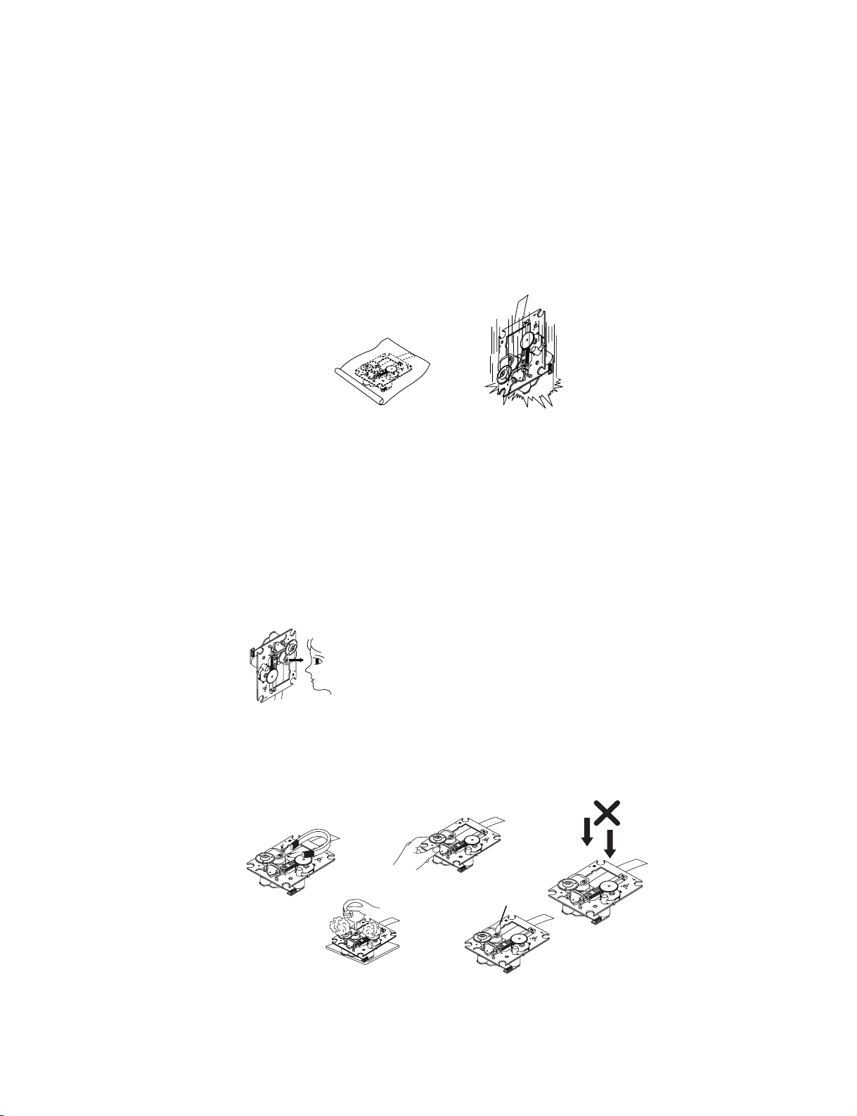
NOTES REGARDING HANDLING OF THE PICK-UP
1. Notes for transport and storage
1) The pick-up should always be left in its conductive bag until immediately prior to use.
2) The pick-up should never be subjected to external pressure or impact.
2. Repair notes
1) The pick-up incorporates a strong magnet, and so should never be brought close to magnetic materials.
2) The pick-up should always be handled correctly and carefully, taking care to avoid external pressure and
impact. If it is subjected to strong pressure or impact, the result may be an operational malfunction and/or
damage to the printed-circuit board.
3) Each and every pick-up is already individually adjusted to a high degree of precision, and for that reason
the adjustment point and installation screws should absolutely never be touched.
4) Laser beams may damage the eyes!
Absolutely never permit laser beams to enter the eyes!
Also NEVER switch ON the power to the laser output part (lens, etc.) of the pick-up if it is damaged.
5) Cleaning the lens surface
If there is dust on the lens surface, the dust should be cleaned away by using an air bush (such as used
for camera lens). The lens is held by a delicate spring. When cleaning the lens surface, therefore, a
cotton swab should be used, taking care not to distort this.
6) Never attempt to disassemble the pick-up.
Spring by excess pressure. If the lens is extremely dirty, apply isopropyl alcohol to the cotton swab. (Do
not use any other liquid cleaners, because they will damage the lens.) Take care not to use too much of
this alcohol on the swab, and do not allow the alcohol to get inside the pick-up.
- 1-2 -
Storage in conductive bag
Drop impact
NEVER look directly at the laser beam, and don’t let
contact fingers or other exposed skin.
Magnet
How to hold the pick-up
Pressure
Pressure
Cotton swab
Conductive Sheet
Page 4
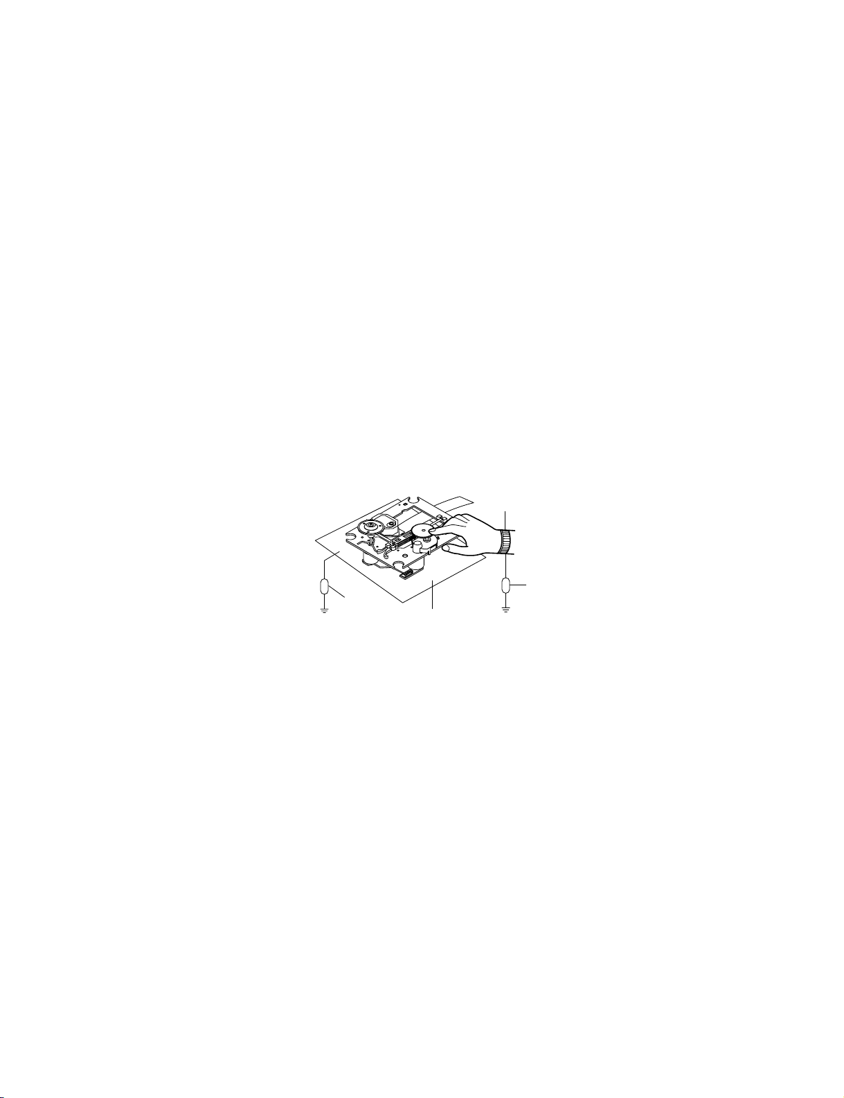
NOTES REGARDING COMPACT DISC PLAYER REPAIRS
1. Preparations
1) Compact disc players incorporate a great many ICs as well as the pick-up (laser diode). These
components are sensitive to, and easily affected by, static electricity. If such static electricity is high
voltage, components can be damaged, and for that reason components should be handled with care.
2) The pick-up is composed of many optical components and other high-precision components. Care must
be taken, therefore, to avoid repair or storage where the temperature of humidity is high, where strong
magnetism is present, or where there is excessive dust.
2. Notes for repair
1) Before replacing a component part, first disconnect the power supply lead wire from the unit
2) All equipment, measuring instruments and tools must be grounded.
3) The workbench should be covered with a conductive sheet and grounded.
When removing the laser pick-up from its conductive bag, do not place the pick-up on the bag. (This is
because there is the possibility of damage by static electricity.)
4) To prevent AC leakage, the metal part of the soldering iron should be grounded.
5) Workers should be grounded by an armband (1MΩ)
6) Care should be taken not to permit the laser pick-up to come in contact with clothing, in order to prevent
static electricity changes in the clothing to escape from the armband.
7) The laser beam from the pick-up should NEVER be directly facing the eyes or bare skin.
- 1-3 -
Armband
Conductive
Sheet
Resistor
(1 Mohm)
Resistor
(1 Mohm)
Page 5
❏
ESD PRECAUTIONS
Electrostatically Sensitive Devices (ESD)
Some semiconductor (solid state) devices can be damaged easily by static electricity. Such components
commonly are called Electrostatically Sensitive Devices (ESD). Examples of typical ESD devices are integrated
circuits and some field-effect transistors and semiconductor chip components. The following techniques should
be used to help reduce the incidence of component damage caused by static electricity.
1. Immediately before handling any semiconductor component or semiconductor-equipped assembly, drain off
any electrostatic charge on your body by touching a known earth ground. Alternatively, obtain and wear a
commercially available discharging wrist strap device, which should be removed for potential shock reasons
prior to applying power to the unit under test.
2. After removing an electrical assembly equipped with ESD devices, place the assembly on a conductive
surface such as aluminum foil, to prevent electrostatic charge buildup or exposure of the assembly.
3. Use only a grounded-tip soldering iron to solder or unsolder ESD devices.
4. Use only an anti-static solder removal device. Some solder removal devices not classified as "anti-static" can
generate electrical charges sufficient to damage ESD devices.
5. Do not use freon-propelled chemicals. These can generate electrical charges sufficient to damage ESD
devices.
6. Do not remove a replacement ESD device from its protective package until immediately before you are ready
to install it. (Most replacement ESD devices are packaged with leads electrically shorted together by
conductive foam, aluminum foil or comparable conductive materials).
7. Immediately before removing the protective material from the leads of a replacement ESD device, touch the
protective material to the chassis or circuit assembly into which the device will by installed.
CAUTION : BE SURE NO POWER IS APPLIED TO THE CHASSIS OR CIRCUIT, AND OBSERVE ALL OTHER
SAFETY PRECAUTIONS.
8. Minimize bodily motions when handing unpackaged replacement ESD devices. (Otherwise harmless motion
such as the brushing together of your clothes fabric or the lifting of your foot from a carpeted floor can
generate static electricity sufficient to damage an ESD device).
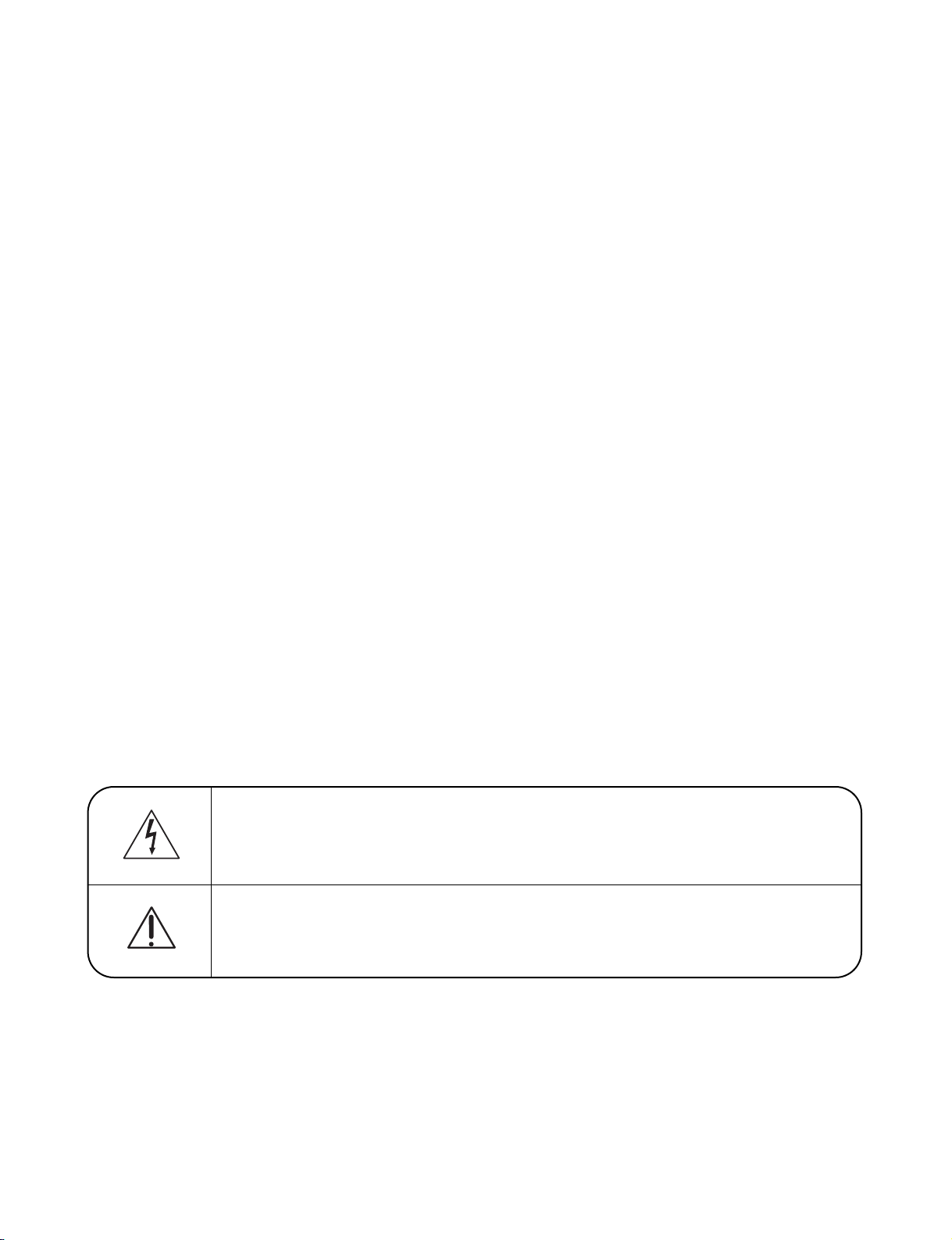
CAUTION. GRAPHIC SYMBOLS
- 1-4 -
THE LIGHTNING FLASH WITH APROWHEAD SYMBOL. WITHIN AN EQUILATERAL
TRIANGLE, IS INTENDED TO ALERT THE SERVICE PERSONNEL TO THE PRESENCE OF
UNINSULATED “DANGEROUS VOLTAGE” THAT MAY BE OF SUFFICIENT MAGNITUDE TO
CONSTITUTE A RISK OF ELECTRIC SHOCK.
THE EXCLAMATION POINT WITHIN AN EQUILATERAL TRIANGLE IS INTENDED TO
ALERT THE SERVICE PERSONNEL TO THE PRESENCE OF IMPORTANT SAFETY
INFORMATION IN SERVICE LITERATURE.
Page 6
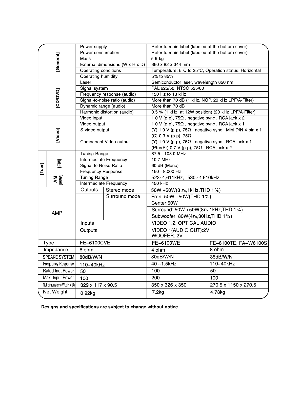
- 1-5 -
❏
SPECIFICATIONS
Page 7
- 1-6 -
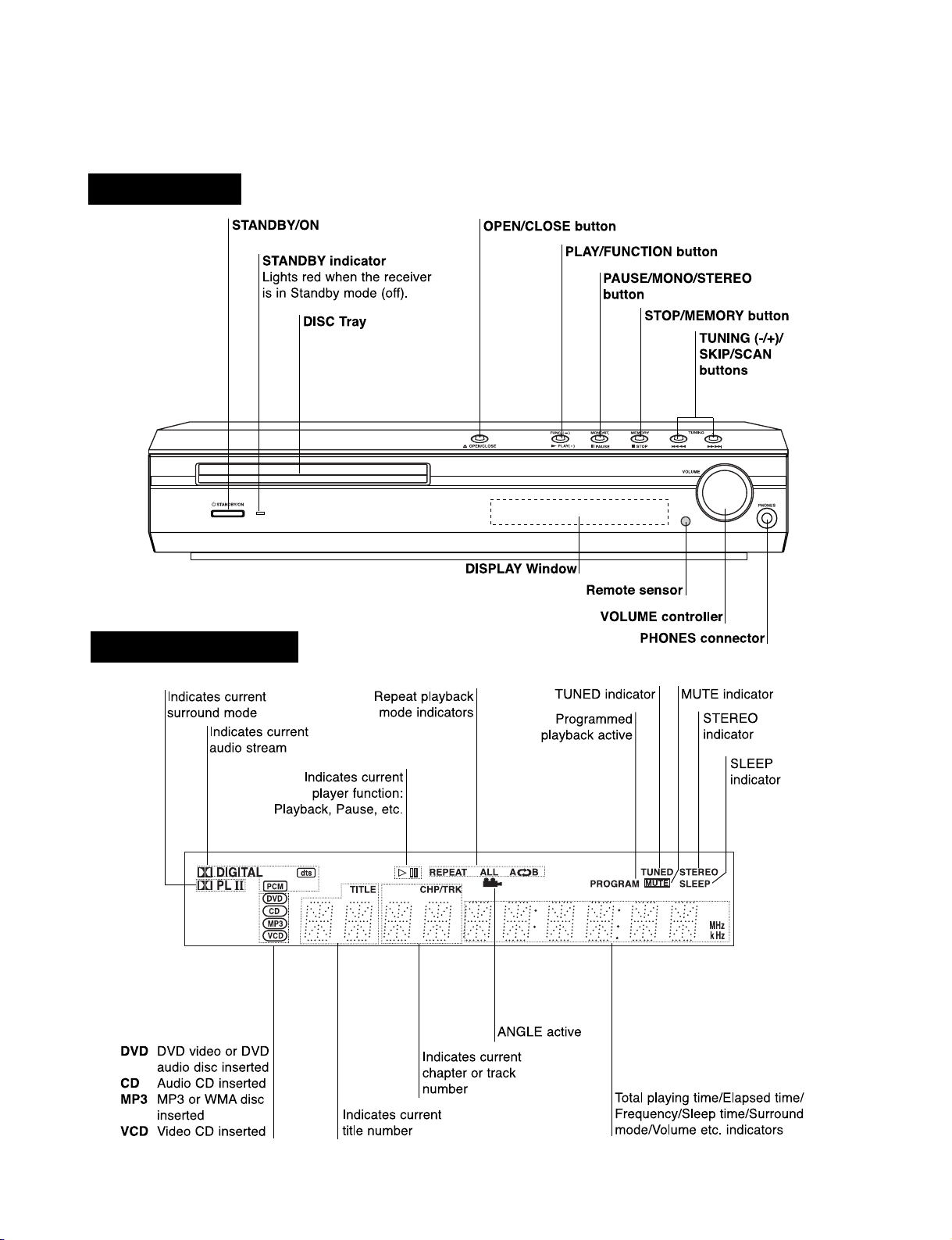
❏
LOCATION OF CUSTOMER CONTROLS
FRONT PANEL
DISPLAY WINDOW
Page 8
- 1-7 -
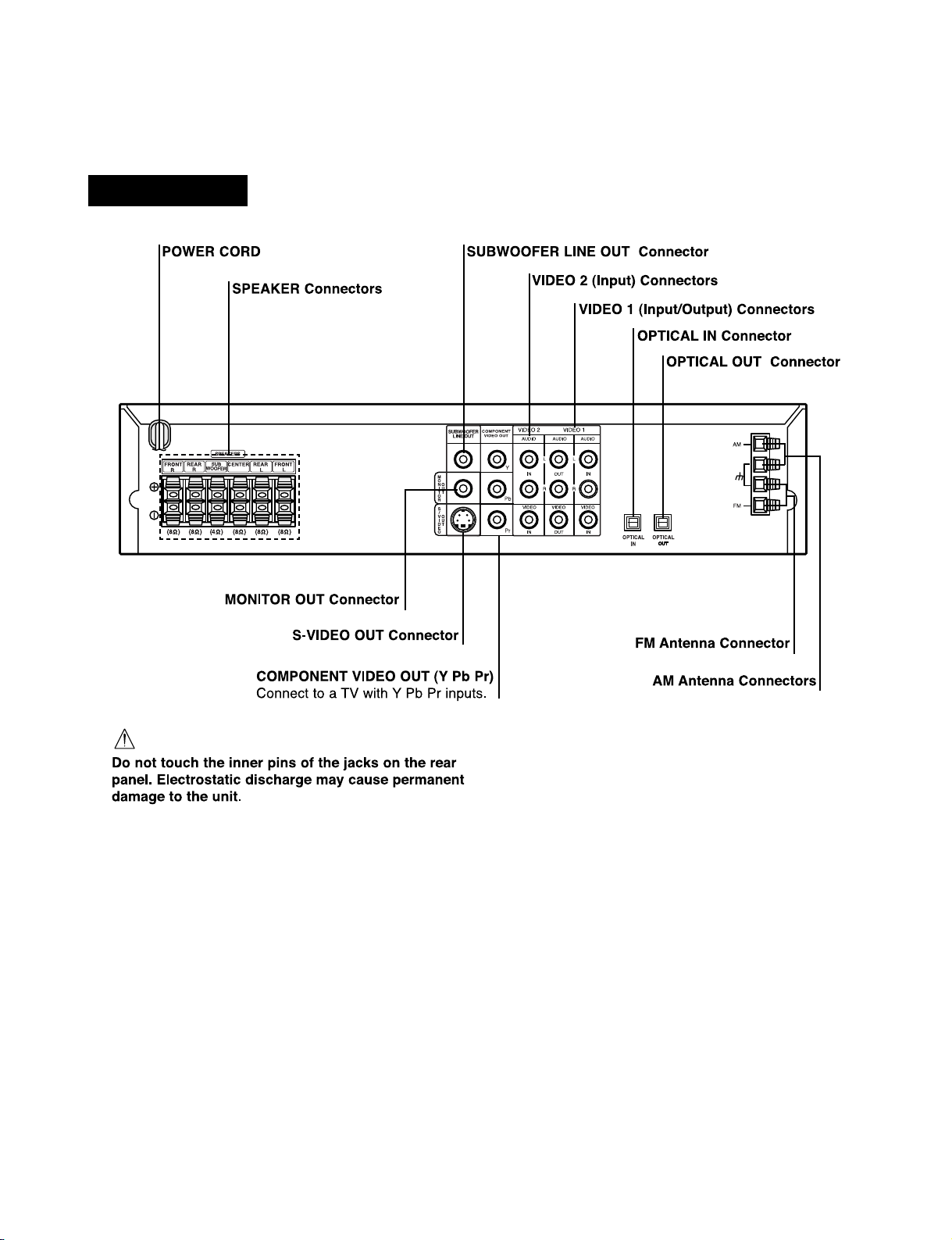
REAR PANEL
Page 9
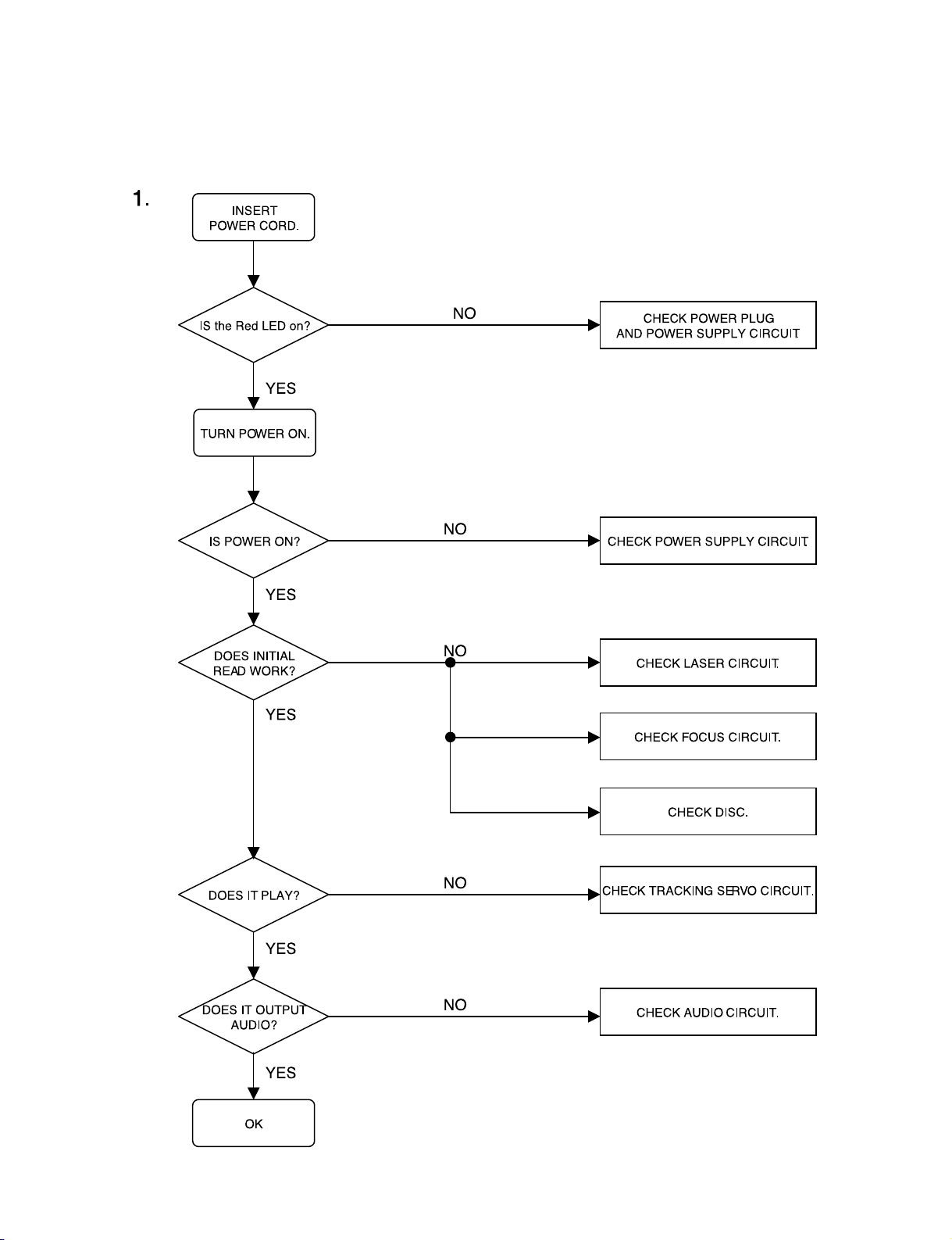
- 2-1 -
SECTION 2. AUDIO PART
❏
ELECTRICAL TROUBLESHOOTING GUIDE
Page 10
- 2-2 -
2. AUDIO µ. COM CIRCUIT
POWER ON
Does CD/DVD
appear at FLT?
Does LOADING
appear at FLD?
Does it appear
DVD Error at
FLD?
Does Video1/2, TV
AUDIO, FM 87.5 appear
at FLD?
OK.
Check
Connector(PN903)if
is normally.
Reconnet it.
Refer to SMPS
Refer to oscillator
Circuit.
Check DVD Reset Waveform.
Check IC101 Reset Wavefrom.
Check 3.3V line.
Check Power dection Circuit..
Check power part
of Main B/D.
Check oscillator
of x101.
Check if PN200
PIN is High.
Check if IC101
PIN is High.
Check if IC101 PIN
, , , is high
(5V).
Check if IC101
PIN
is High .
Replace IC101.
Does no Dise or
Time appear at FLD?
Check if DVD an Audio
Micom Interface is OK.
Check power.
Check DVD Module.
Check SMPS.
17
46 72
90
11
5
26
Page 11
- 2-3 -
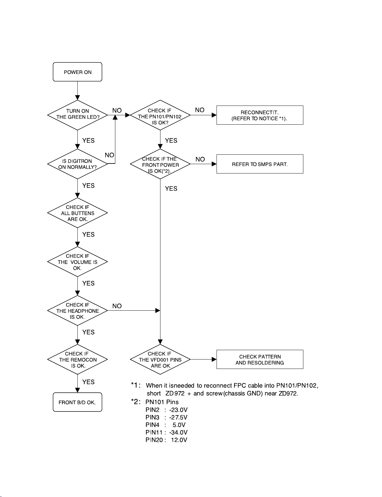
3. FRONT CIRCUIT (1/2)
Page 12
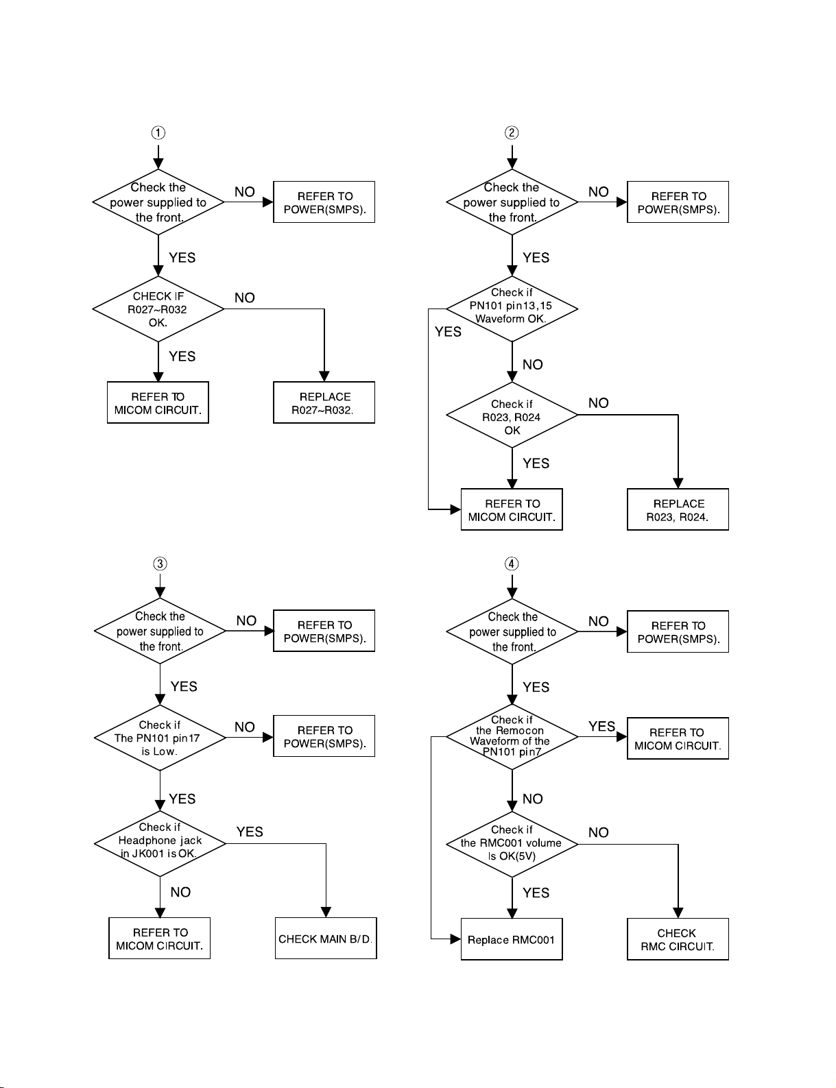
- 2-4 -
4. FRONT CIRCUIT (2/2)
Page 13

- 2-5 -
MEMO
Page 14
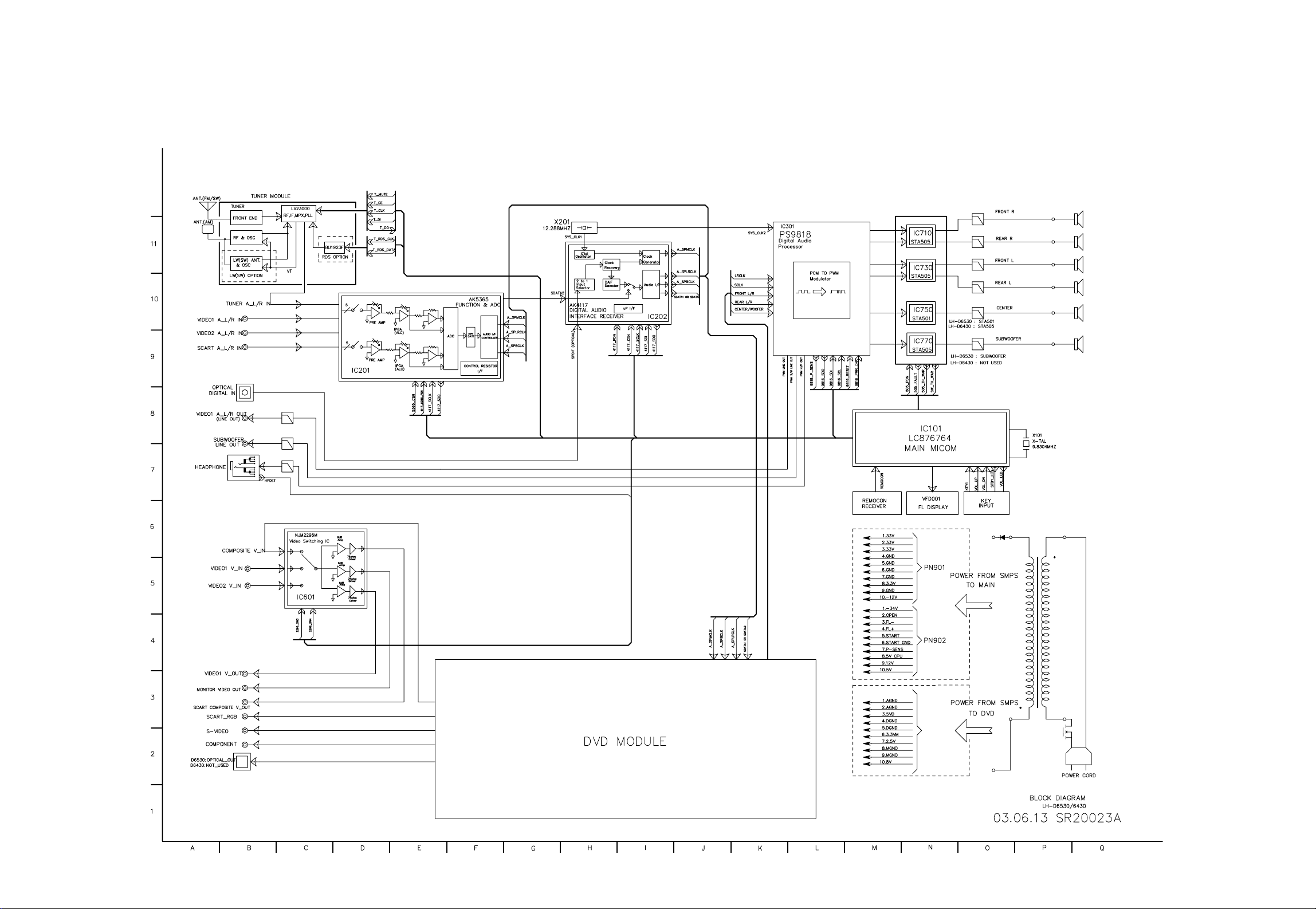
2-6 2-7
❏
BLOCK DIAGRAM
Page 15
2-8 2-9
❏
SHEMATIC DIAGRAMS
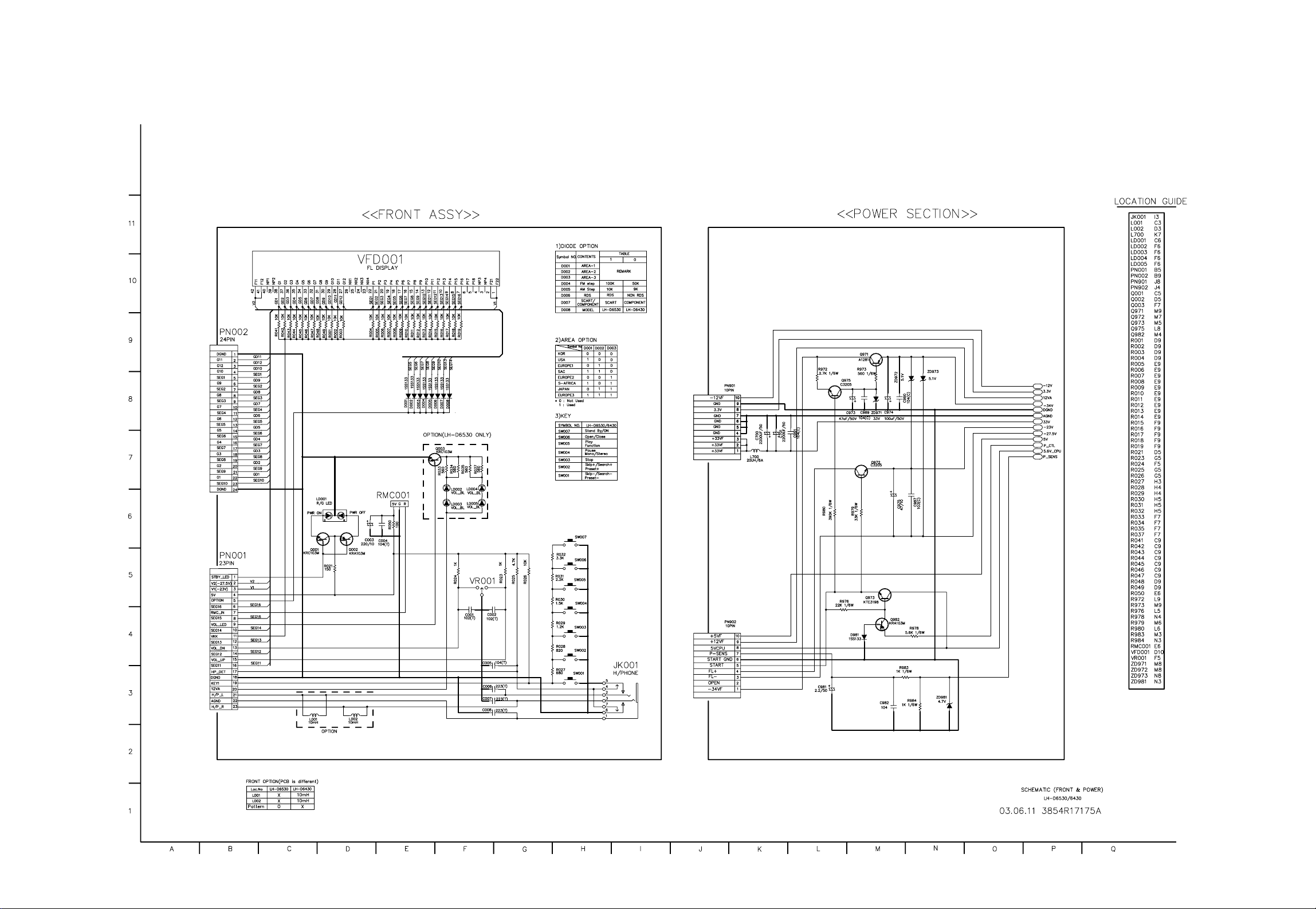
• FRONT & POWER SCHEMATIC DIAGRAM
Page 16
2-10 2-11
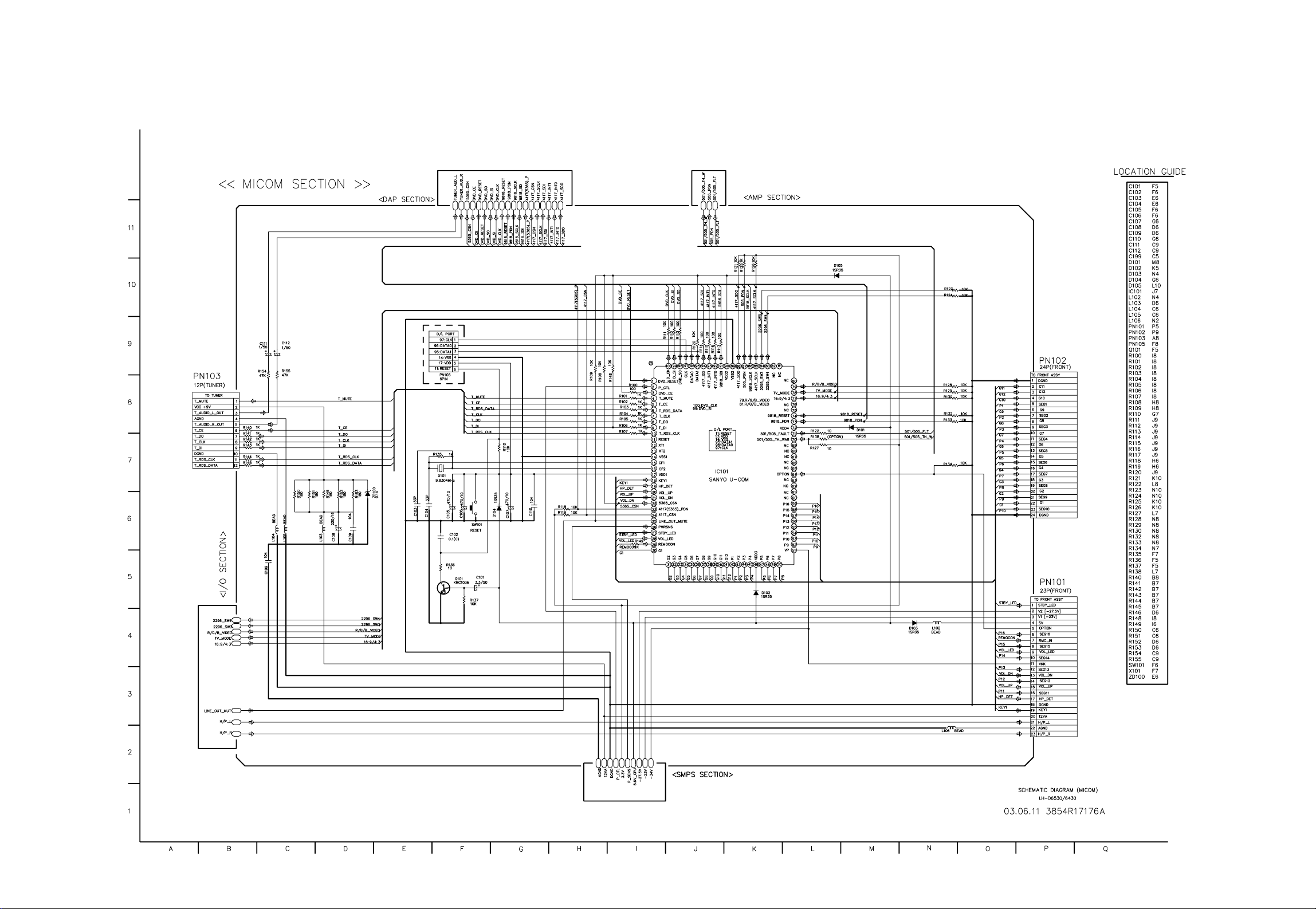
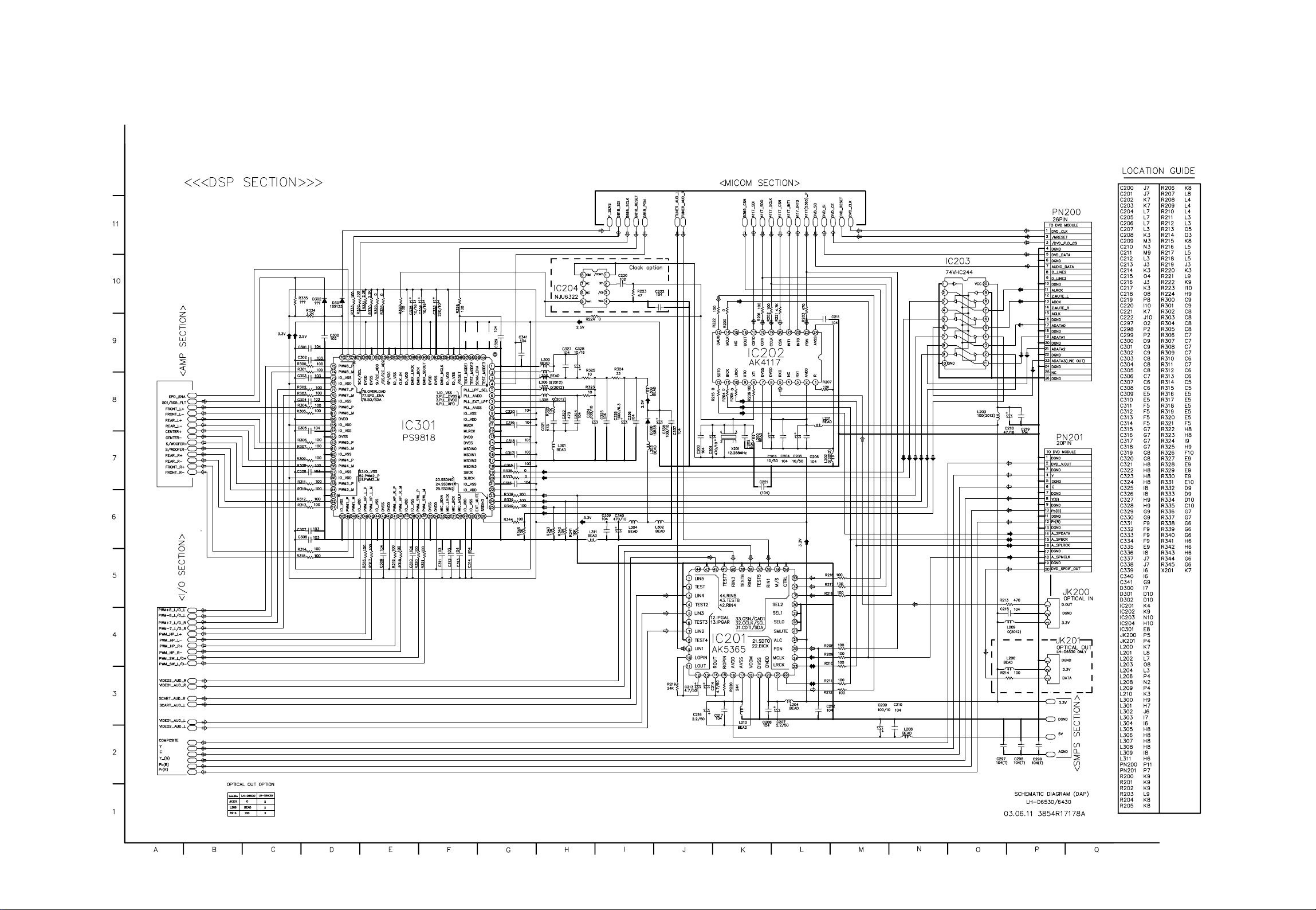
• MICOM SCHEMATIC DIAGRAM
Page 17
2-12 2-13
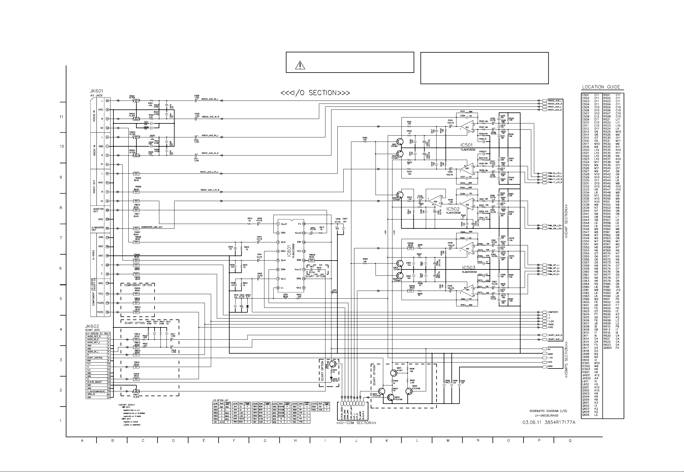
• I/O SCHEMATIC DIAGRAM
NOTE: Warning
Parts that are shaded are critical With respect
to risk of fire or electrical shock.
NOTE:
1. Shaded(■) parts are critical for safety.Replace only
with specified part number.
2. Voltages are DC-measured with a digital voltmefer
during Play mode.
Page 18
2-14 2-15
• DAP SCHEMATIC DIAGRAM
Page 19
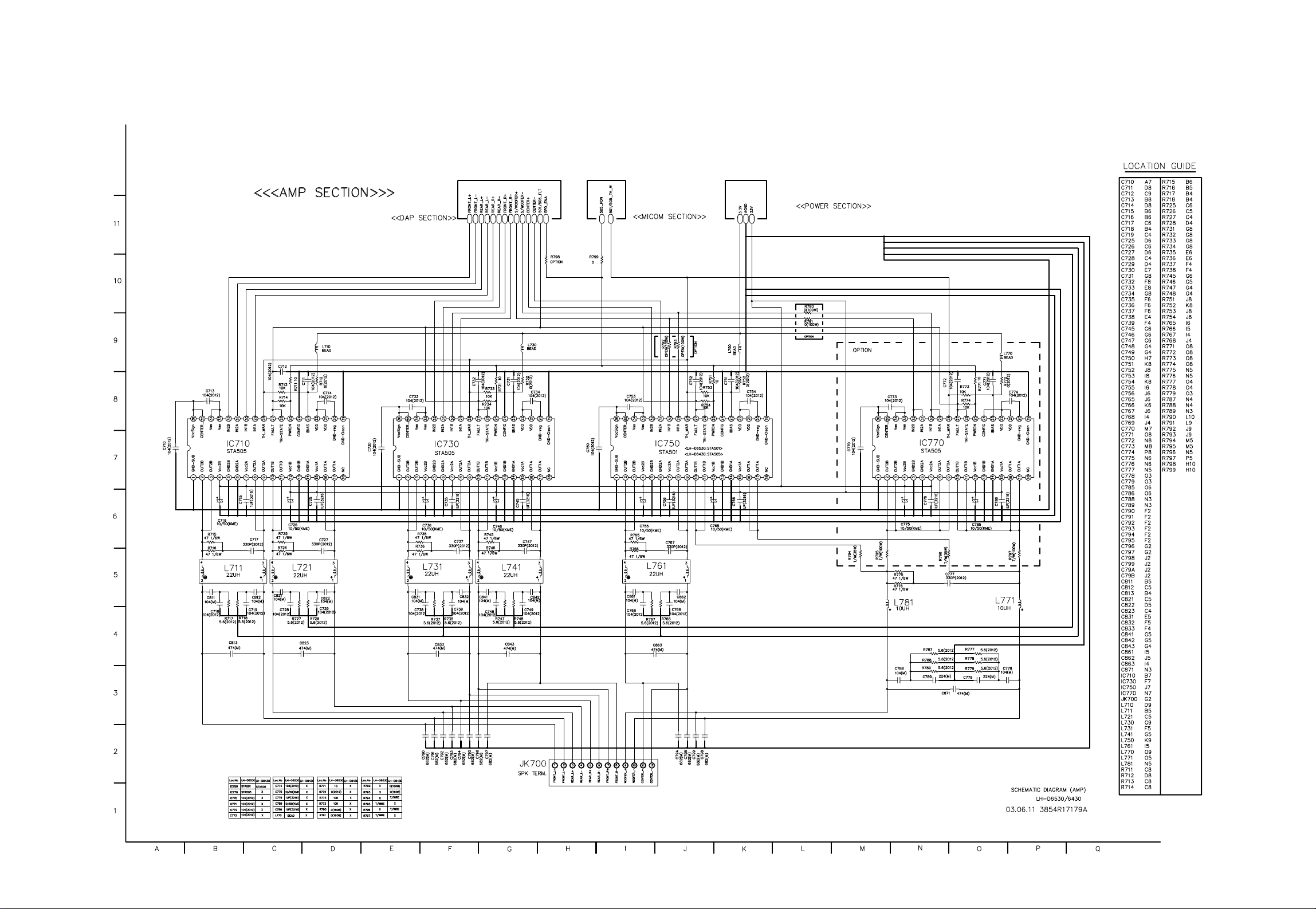
• AMP SCHEMATIC DIAGRAM
2-16 2-17
Page 20
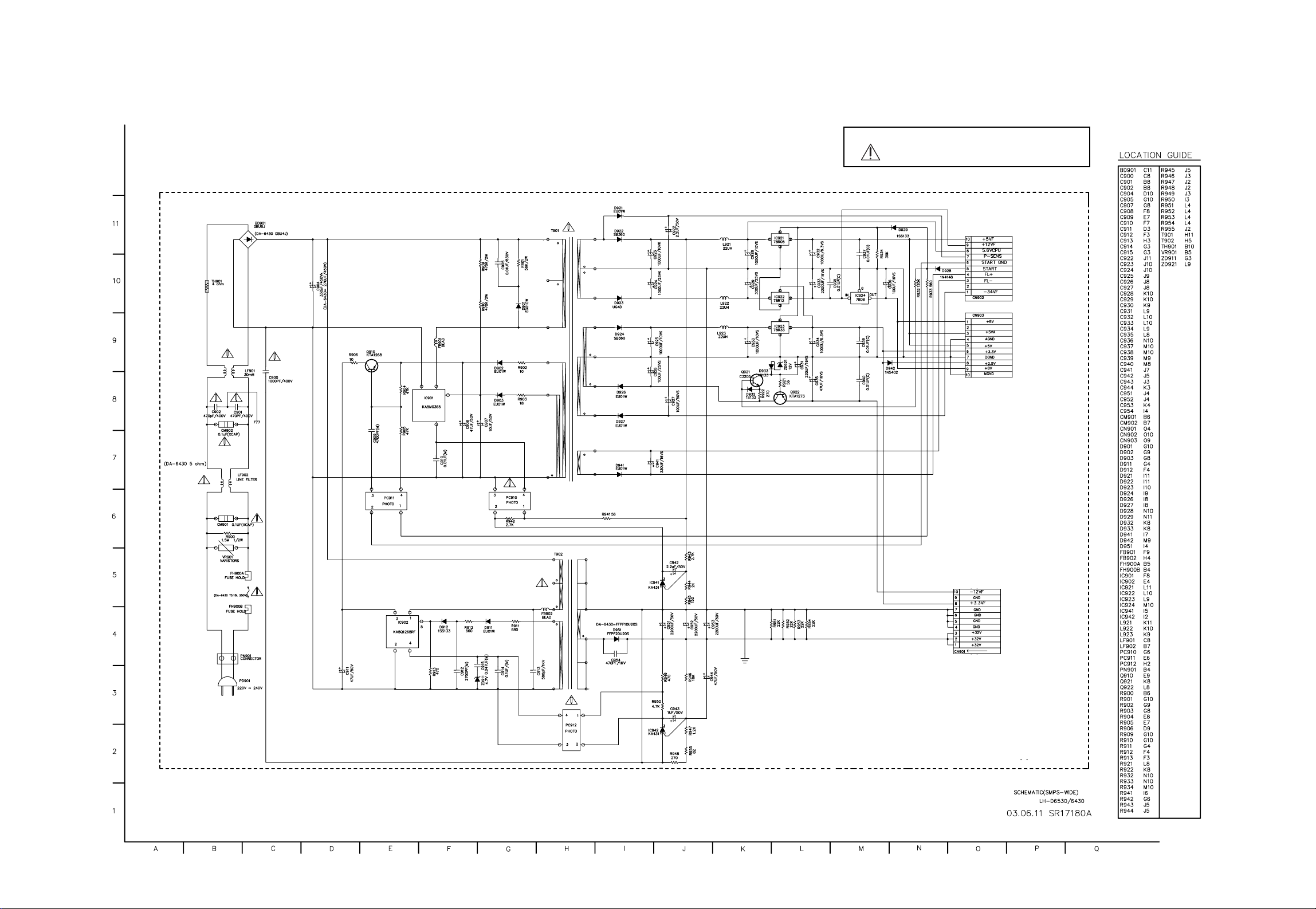
• SMPS SCHEMATIC DIAGRAM
2-18 2-19
NOTE: Warning
Parts that are shaded are critical With respect
to risk of fire or electrical shock.
Page 21
2-20 2-21
❏ WIRING DIAGRAM
NOTE: Warning
Parts that are shaded are critical With respect
to risk of fire or electrical shock.
Page 22
2-22 2-23
1.LH-D6530(MAIN)
1).IC101(LC876748C-52K, MICOM)
PIN No. Volt(V) PIN No. Volt(V) PIN No. Volt(V) PIN No. Volt(V) PIN No. Volt(V)
1 2.15V 21 4.88V 41 -31.V 61 81
2 4.8V 22 3.94V 42 -28.V 62 82
3 1.36V 23 3.26V 43 -29.V 63 83
4 24 3.26V 44 -25.V 64 2.2V 84
5 25 0 45 -32.V 65 85 3.3V
6 26 2.75V 46 4.85V 66 86 1.8V
7 27 4.85V 47 -31.V 67 87 3.17V
8 28 4.85V 48 -31.V 68 88 3.3V
9 29 49 -26.V 69 89 0
10 30 -31.V 50 -25.V 70 3.26V 90 4.88V
11 31 -31.V 51 -32.V 71 3.15V 91 1.5V
12 32 -31.V 52 -26.V 72 5.V 92
13 33 -31.V 53 -26.V 73 4.95V 93
14 0 34 -31.V 54 -26.V 74 4.96V 94
15
2.68V(9.8304MHz)
35 -31.V 55 -26.V 75 95 0
16
2.94V(9.8304MHz)
36 -31.V 56 -32.V 76 96 0
17 4.89V 37 -31.V 57 -32.V 77 97 0
18 4.86V 38 -31.V 58 -32.V 78 98 2.7V
19 39 -31.V 59 -25.V 79 99 2.6V
20 4.88V 40 -31.V 60 0 80 100 2.6V
2).IC201(AK5365VQ, ADC & FUCTION IC)
PIN No. Volt(V) PIN No. Volt(V) PIN No. Volt(V) PIN No. Volt(V)
1 12 2.5V 23 LRCK 34 0
2 0 13 2.5V 24 MCLK 35 0
3
ADATA4_L_IN
14 2.5V 25 3.3V 36
ADATA1_R_IN
4 0 15 2.5V 26 3.3V 37 0
5
ADATA3_L_IN
16 5.V 27 0 38
ADATA2_R_IN
6 0 17 0 28 0 39 0
7
ADATA2_L_IN
18 2.5V 29 0 40
ADATA3_R_IN
8 0 19 0 30 0 41 0
9
ADATA1_L_IN
20 3.3V 31 3.3V 42
ADATA4_R_IN
10 2.5V 21
ADATA_OUT
32 3.3V 43 0
11 2.5V 22 BCK 33 3.9V 44
3).IC202(AK4117VF-E2, DIR IC)
PIN No. Volt(V) PIN No. Volt(V)
10 13
ADATA_IN
2 3.3V 14 MCLK
315
416
5 SPDIF_IN 17
6 3.3V 18
7 0 19 3.3V
8
2.2V(12.288MHz)
20 3.3V
921
10 LRCK 22
11 BCK 23 3.3V
12
ADATA_OUT
24 0
4).IC203(74VHC244MTCX, BUFFER IC)
PIN No. Volt(V) PIN No. Volt(V)
1 0 11 ADATA1
2 0 12 ADATA2
3 LRCK 13 ADATA0
4 14 ADATA3
5 BCK 15 BCK
6 ADATA3 16
7 ADATA0 17 LRCK
8 ADATA2 18 0
9 ADATA1 19 0
10 0 20 3.2V
5).IC301(PS9818, DAP IC)
PIN No. Volt(V) PIN No. Volt(V) PIN No. Volt(V) PIN No. Volt(V) PIN No. Volt(V)
1 0 21 0 41
PWM_OUT
61
PWM_OUT
81 0
2 0 22 3.3V 42 2.5V 62
PWM_OUT
82 3.3V
3 2.35V 23 ADATA0 43 0 63 0 83 3.3V
4 5.V 24 ADATA1 44 0 64 0 84 0
5 2.35V 25 ADATA2 45
PWM_OUT
65 3.3V 85 0
6 2.32V 26 ADATA3 46
PWM_OUT
66 2.5V 86
2.27(12.288MHz)
7 0.89V 27 47 3.3V 67
PWM_OUT
87 3.3V
8 0 28 0 48
PWM_OUT
68
PWM_OUT
88
9 0 29 3.3V 49
PWM_OUT
69 0 89
10 3.3V 30 50 0 70
PWM_OUT
90
11 0 31 51
PWM_OUT
71
PWM_OUT
91 2.5V
12 0 32 52
PWM_OUT
72 3.3V 92 0
13 2.5V 33 53 0 73 0 93
14 0 34 2.5V 54
PWM_OUT
74
PWM_OUT
94 3.3V
15 0 35 0 55
PWM_OUT
75
PWM_OUT
95 0
16 0 36
PWM_OUT
56 3.3V 76 3.2V 96 4.89V
17 0 37
PWM_OUT
57 0 77 0 97
18 0 38 0 58
PWM_OUT
78 1.5V 98
19 BCK 39 3 59
PWM_OUT
79 1.8V 99
20 LRCK 40
PWM_OUT
60 0 80 2.5V 100
6).IC501(NJM4580M, OP AMP IC)
PIN No. Volt(V) PIN No. Volt(V)
1
Audio1_L_OUT
5
Audio1_R+_IN
2
Audio1_L-_IN
6
Audio1_R-_IN
3
Audio1_L+_IN
7
Audio1_R_OUT
4 -11.8V 8
7).IC502(NJM4580M, OP AMP IC)
PIN No. Volt(V) PIN No. Volt(V)
1 S/W_OUT 5 S/W_OUT
2 S/W-_IN 6 S/W_OUT
3 S/W+_IN 7 S/W_OUT
4 -11.8V 8 11.9V
8).IC503(NJM4580M, OP AMP IC)
PIN No. Volt(V) PIN No. Volt(V)
1
H/Phone_L_OUT
5
H/Phone_R+_IN
2
H/Phone_L-_IN
6
H/Phone_R-_IN
❏
VOLTAGE SHEET (IC&TR)
Page 23
2-24 2-25
3
H/Phone_L+_IN
7
H/Phone_R_OUT
4 -11.8V 8 11.9V
9).IC601(NJM2296M, VIDEO SWITCHING IC)
PIN No. Volt(V) PIN No. Volt(V)
1 Video_OUT 9
2 5.V 10 5.V
3 Video2_IN 11 Video_OUT
4120
5 Video1_IN 13
6 14 5.V
7
COMPOSITE_IN
15 Video_OUT
8 -12.V 16 5.V
10).IC710(STA505, DIGITAL AMP IC)
PIN No. Volt(V) PIN No. Volt(V) PIN No. Volt(V) PIN No. Volt(V)
10 10
REAR_L+_OUT
19 0 28 3.28V
2
FRONT_L+_OUT
11
REAR_L+_OUT
20 0 29 REAR_L- _IN
3
FRONT_L+_OUT
12 31.5V 21 4.89V 30
REAR_L+_IN
4 31.5V 13 0 22 4.89V 31
FRONT_L-_IN
5 0 14 0 23 3.3V 32
FRONT_L+_IN
6 0 15 31.5V 24 0 33 26.36V
7 31.5V 16
REAR_L-_OUT
25 3.18V 34 26.36V
8
FRONT_L-_OUT
17
REAR_L-_OUT
26 3.16V 35 31.42V
9
FRONT_L-_OUT
18 27 3.16V 36 31.42V
11).IC730(STA505, DIGITAL AMP IC)
PIN No. Volt(V) PIN No. Volt(V) PIN No. Volt(V) PIN No. Volt(V)
10 10
FRONT_R+_OUT
19 0 28 3.28V
2
REAR_R+_OUT
11
FRONT_R+_OUT
20 0 29s
FRONT_R-_IN
3
REAR_R+_OUT
12 31.5V 21 4.89V 30
FRONT_R+_IN
4 31.5V 13 0 22 4.89V 31
REAR_R-_IN
5 0 14 0 23 3.3V 32
REAR_R+_IN
6 0 15 31.5V 24 0 33 26.36V
7 31.5V 16
FRONT_R-_OUT
25 3.18V 34 26.36V
8
REAR_R-_OUT
17
FRONT_R-_OUT
26 3.16V 35 31.42V
9
REAR_R-_OUT
18 27 3.16V 36 31.42V
12).IC750(STA501, DIGITAL AMP IC)
PIN No. Volt(V) PIN No. Volt(V) PIN No. Volt(V) PIN No. Volt(V)
1 0 10 19 0 28 3.28V
2
CENTER+_OUT
11 20 0 29
3
CENTER+_OUT
12 31.5V 21 4.89V 30
4 31.5V 13 0 22 4.89V 31
CENTER-_IN
5 0 14 0 23 3.3V 32
CENTER+_IN
6 0 15 31.5V 24 0 33 26.36V
7 31.5V 16 25 3.18V 34 26.36V
8
CENTER-_OUT
17 26 3.16V 35 31.42V
9
CENTER-_OUT
18 27 3.16V 36 31.42V
13).IC770(STA505, DIGITAL AMP IC)
PIN No. Volt(V) PIN No. Volt(V) PIN No. Volt(V) PIN No. Volt(V)
10 10
WOOFER-_OUT
19 0 28 3.28V
2
WOOFER+_OUT
11
WOOFER-_OUT
20 0 29
WOOFER-_IN
3
WOOFER+_OUT
12 31.5V 21 4.89V 30
WOOFER-_IN
4 31.5V 13 0 22 4.89V 31
WOOFER+_IN
5 0 14 0 23 3.3V 32
WOOFER+_IN
6 0 15 31.5V 24 0 33 26.36V
7 31.5V 16
WOOFER-_OUT
25 3.18V 34 26.36V
8
WOOFER+_OUT
17
WOOFER-_OUT
26 3.16V 35 31.42V
9
WOOFER+_OUT
18 27 3.16V 36 31.42V
2.LH-D6530(SMPS)
1).IC901(KA5M0365R-YDTU, PWM IC)
PIN No. Volt(V)
1 GND
2 300V
3 12V
4 0 ~ 6V
2).IC902(KA5Q1265RF-YDTU, PWM IC)
PIN No. Volt(V)
1 300V
2 GND
3 15V
4 0 ~ 6.5V
5 0 ~ 3V
3).IC921(KA378R05-TSTU, REGULATOR IC)
PIN No. Volt(V)
1 5.6V
25V
3 GND
4 2.5V
4).IC922(KA78R12TSTU, REGULATOR IC)
PIN No. Volt(V)
1 13V
2 12V
3 GND
4 3.3V
5).IC923(KA78R33TSTU, REGULATOR IC)
PIN No. Volt(V)
1 4.5V
2 3.3V
3 GND
4 2.5V
6).IC924(KIA7808API-CU, REGULATOR IC)
PIN No. Volt(V)
1 12V
2 GND
38V
7).IC941(KA431AZ, REGULATOR IC)
PIN No. Volt(V)
1 2.5V
2 GND
3 4.8V
8).IC942(KA431AZ, REGULATOR IC)
PIN No. Volt(V)
1 2.5V
2 GND
3 30V
Page 24
2-26 2-27
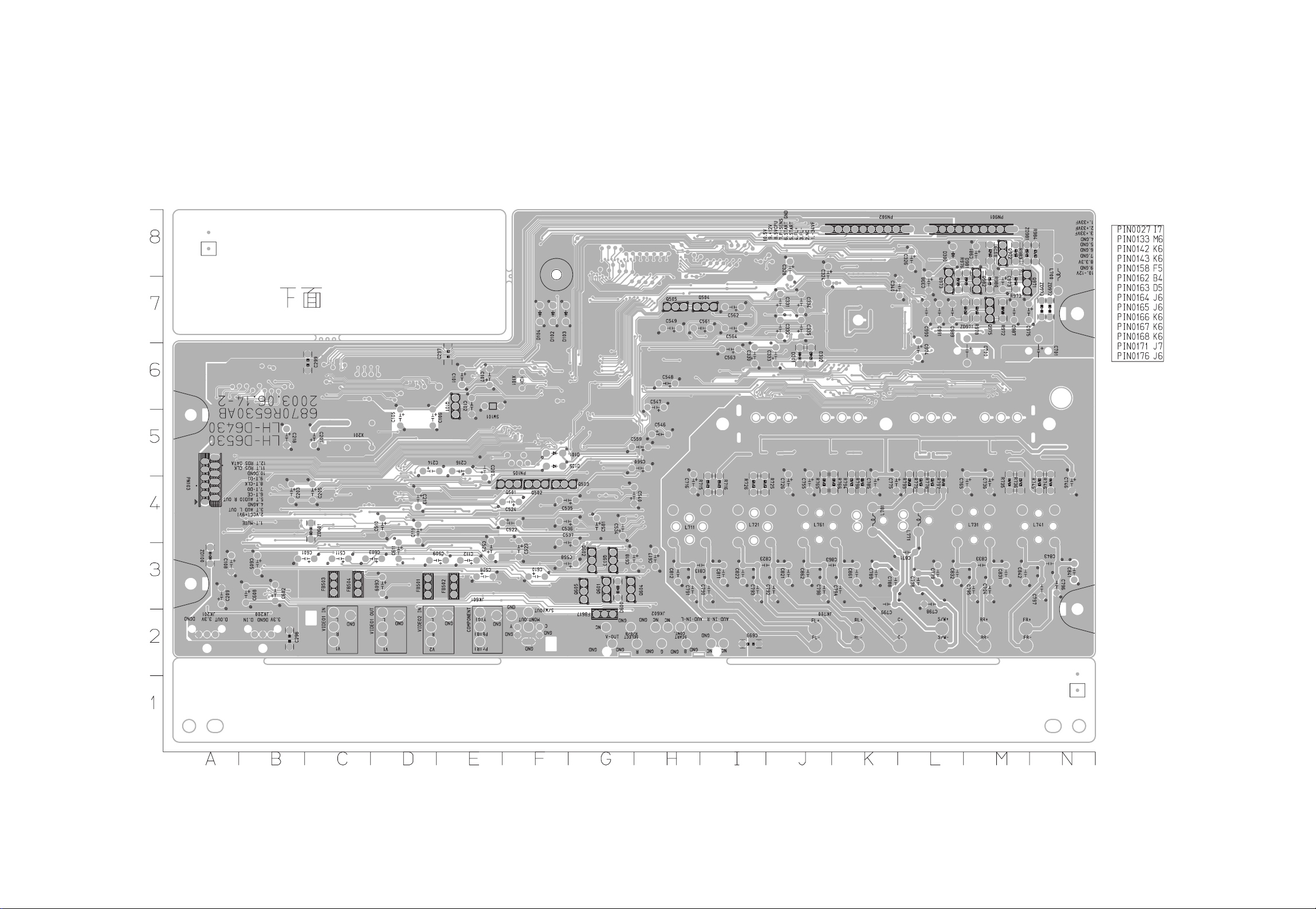
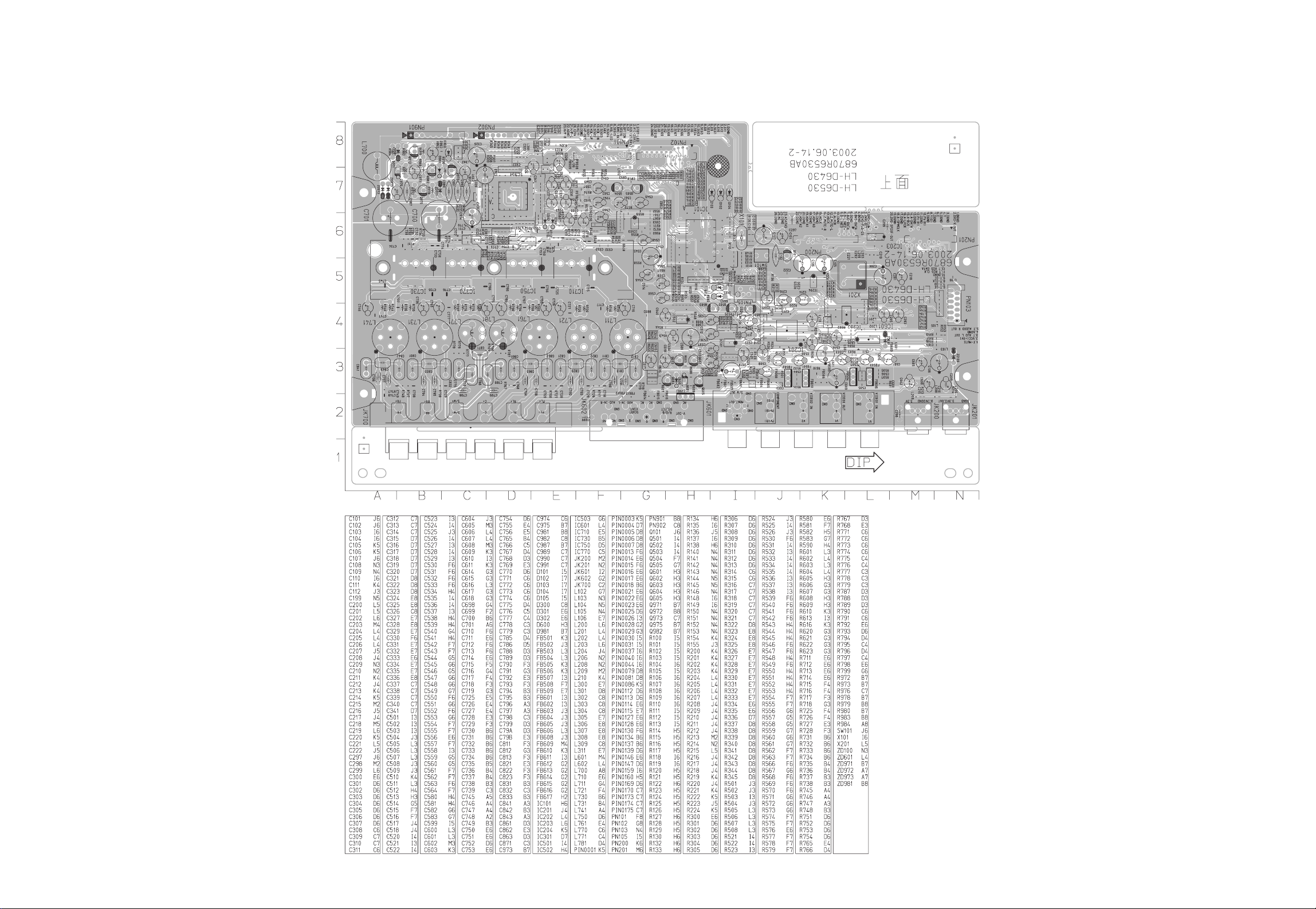
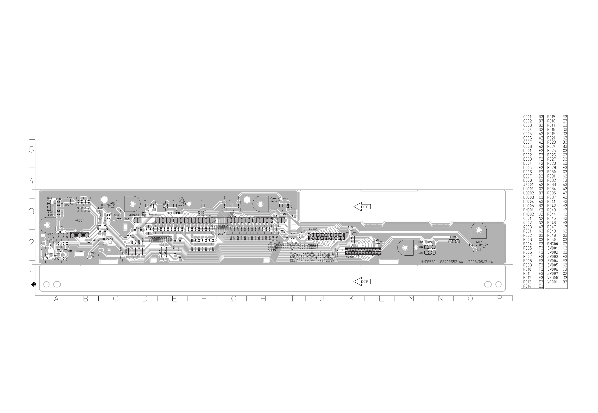
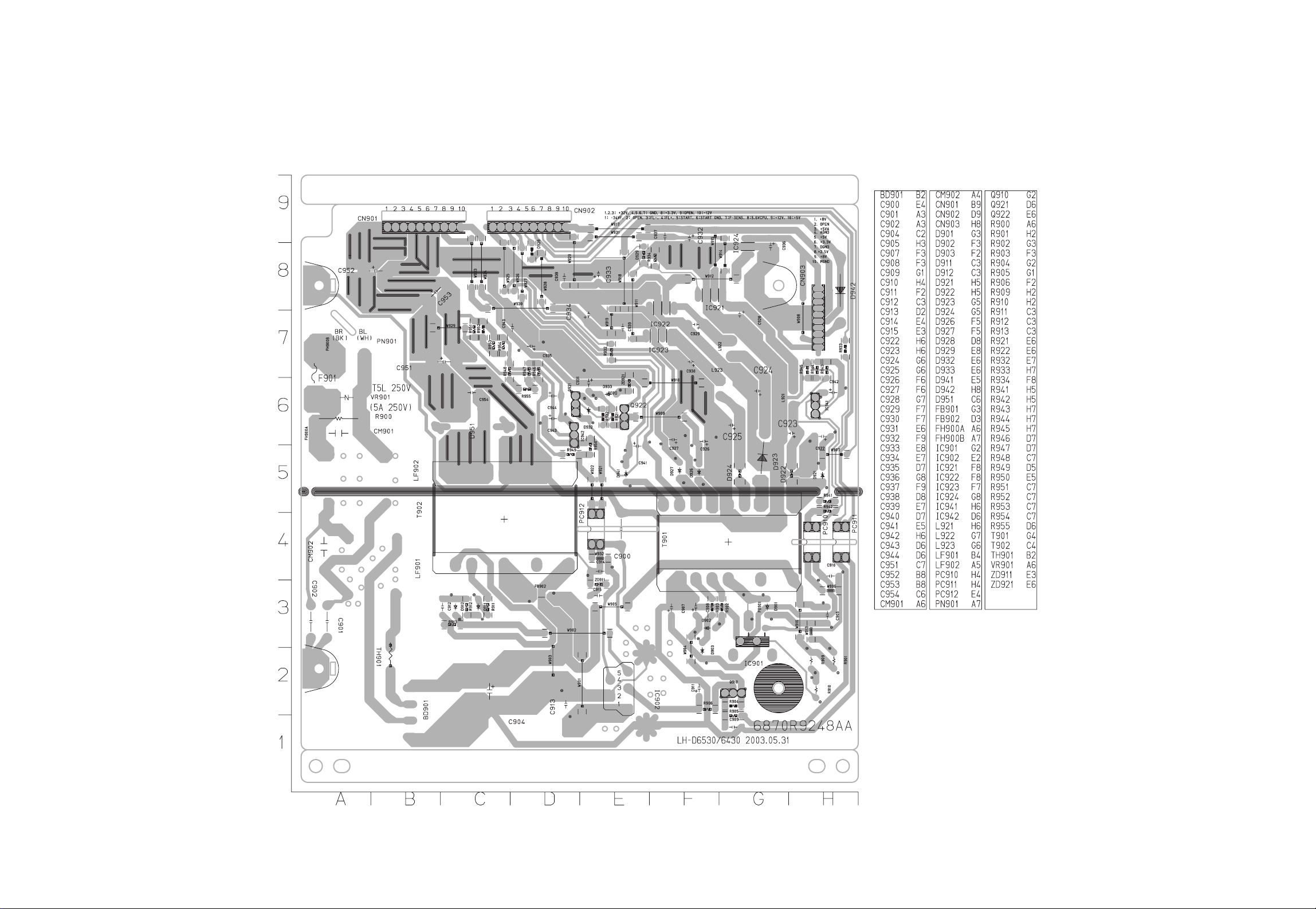
❏
PRINTED CIRCUIT DIAGRAMS
• MAIN P.C BOARD (SOLDER SIDE)
Page 25
2-28 2-29
• MAIN P.C BOARD (COMPONENT SIDE)
Page 26
2-30 2-31
• FRONT P.C. BOARD
Page 27
2-32 2-33
• SMPS P.C. BOARD
Page 28
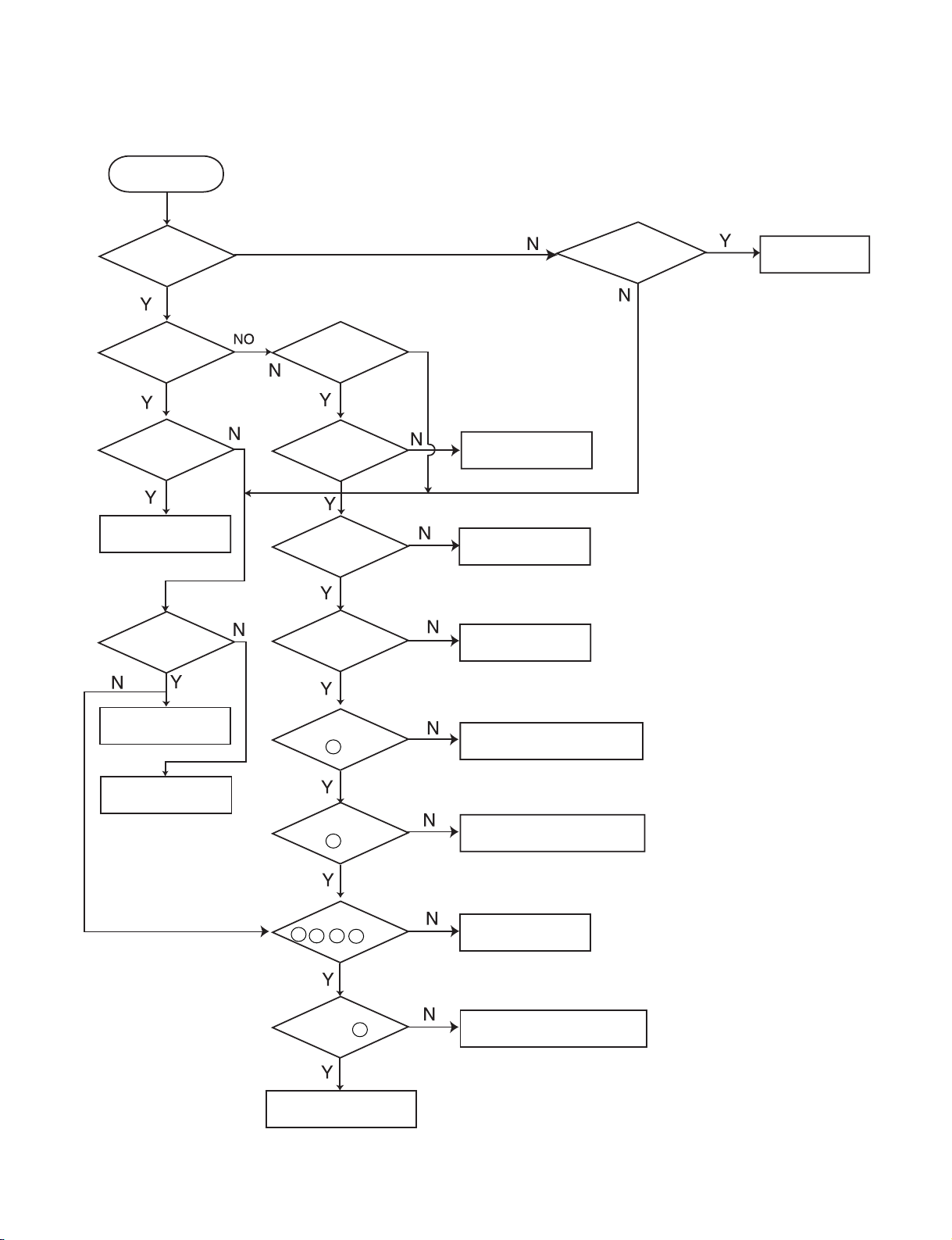
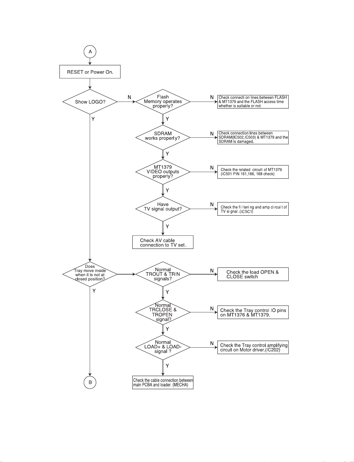
- 3-1 -
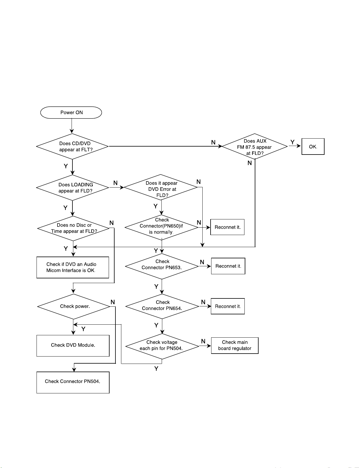
SECTION 3. DVD PART
1. Power check flow
❏
ELECTRICAL TROUBLESHOOTING GUIDE
Page 29
- 3-2 -
2. Test & debug flow
Page 30
- 3-3 -
Page 31

- 3-4 -
Page 32

- 3-5 -
Page 33

- 3-6 -
Page 34

- 3-7 -
Page 35

- 3-8 -
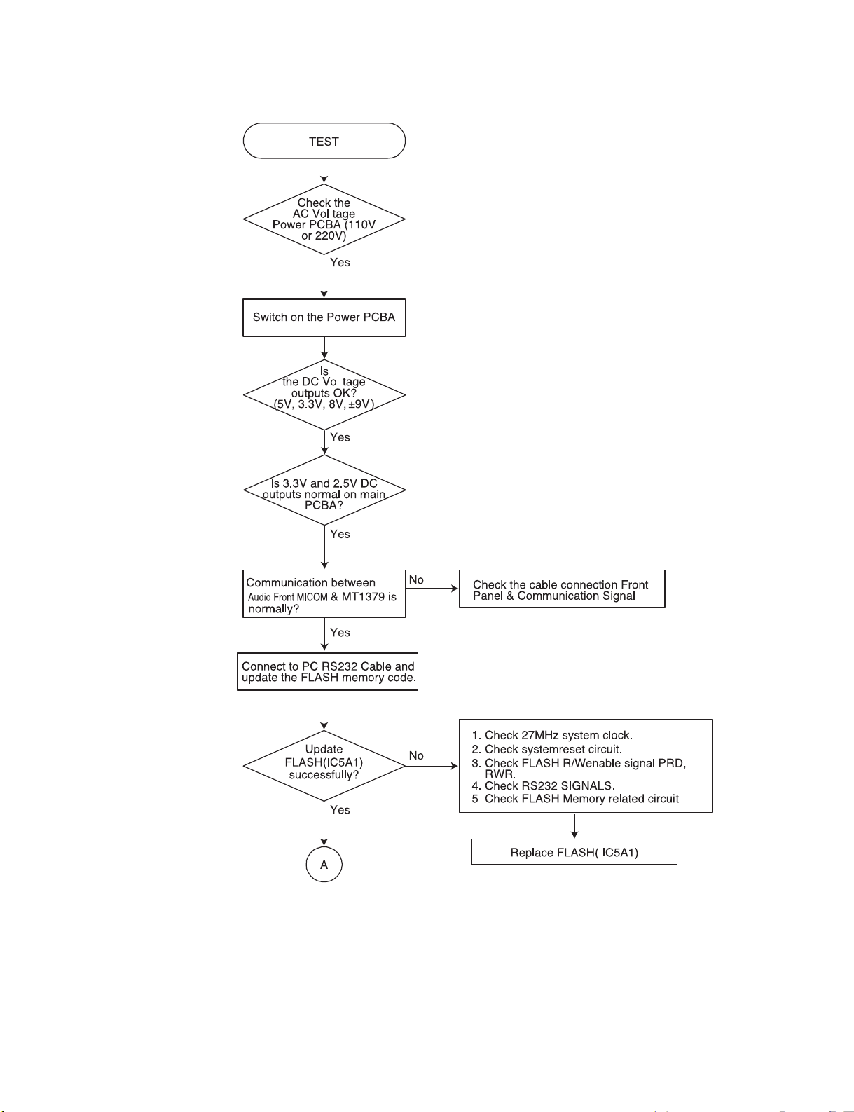
❏
DETAILS AND WAVEFORMS ON SYSTEM TEST
AND DEBUGGING
1. SYSTEM 27MHz CLOCK,RESET,FLASH R/W SIGNAL
1) MT1379 main clock is at 27MHz(X501)
2) MT1336 reset is high active
Page 36

- 3-9 -
3) RS232 waveform during procedure(Downloading)
4) Flash R/W enable signal during download(Downloading)
Page 37

- 3-10 -
2. SDRAM CLOCK
1) MT1379 main clock is at 27MHz(X501)
3. TRAY OPEN/CLOSE SIGNAL
1) Tray open/close waveform
Page 38

- 3-11 -
2) Tray close waveform
3) Tray open waveform
Page 39

- 3-12 -
4. SLED CONTROL RELATED SIGNAL (NO DISC CONDITION)
5. LENS CONTROL RELATED SIGNAL(NO DISC CONDITION)
Page 40

- 3-13 -
6. LASER POWER CONTROL RELATED SIGNAL
(NO DISC CONDITION)
7. DISC TYPE JUDGEMENT WAVEFORM
Page 41

- 3-14 -
Page 42
- 3-15 -
8. FOCUS ON WAVEFORM
Page 43

- 3-16 -
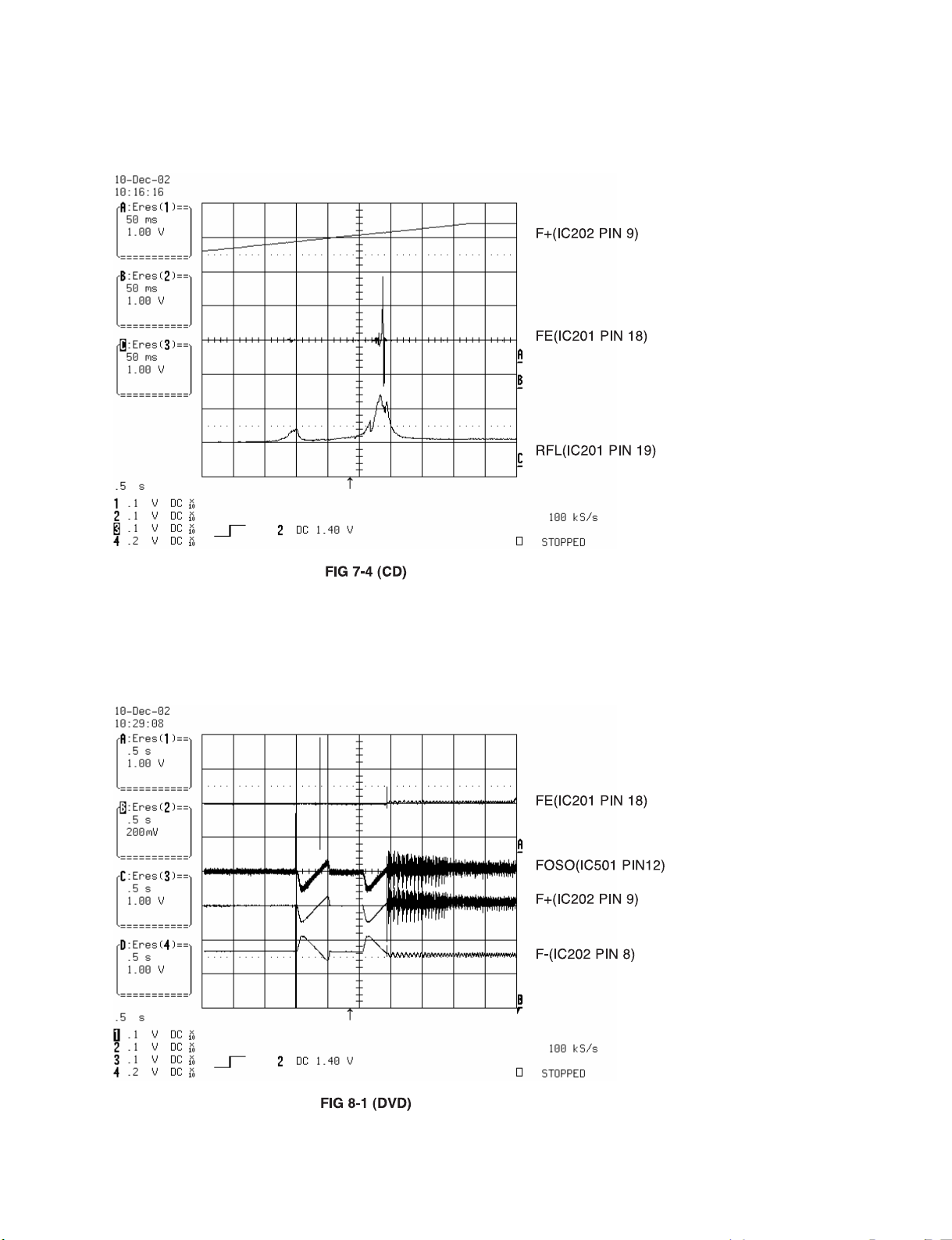
9. SPINDLE CONTROL WAVEFORM (NO DISC CONDITION)
Page 44

- 3-17 -
10. TRACKING CONTROL RELATED SIGNAL(System checking)
Page 45

- 3-18 -
11. RF WAVEFORM
12. MT1379 AUDIO OPTICAL AND COAXIAL OUTPUT (ASPDIF)
Page 46

- 3-19 -
13. MT1379 VIDEO OUTPUT WAVEFORM
1) Full colorbar signal(CVBS)
2) Y
Page 47

- 3-20 -
3) C
14. AUDIO OUTPUT FORM AUDIO DAC
1) Audio related Signal
Page 48

3-21 3-22
❏
DVD PART SCHEMATIC DIAGRAMS
• MPEG SCHEMATIC DIAGRAM
Page 49

3-243-23
• SERVO SCHEMATIC DIAGRAM
Page 50

• INTERFACE SCHEMATIC DIAGRAM
3-263-25
Page 51

3-27 3-28
❏
VOLTAGE SHEET (IC&TR)
Page 52

3-29 3-30
❏
PRINTED CIRCUIT DIAGRAM
• DVD P.C. BOARD(SOLDER SIDE)
Page 53

3-31 3-32
• DVD P.C. BOARD (COMPONENT SIDE)
Page 54

4-1 4-2
351
301
268
302
303
A46
A41
A26
275
266
267
A43
270
272
264
265
250
260
269
305
A47
TUNER
454
454
SECTION 4. EXPLODED VIEWS
• CABINET AND MAIN FRAME SECTION
NOTE) Refer to “SECTION 6 REPLACEMENT
PARTS LIST” in order to look for the
part number of each part.
Page 55

4-3 4-4
• Deck Mechanism Exploded View
LOCA.NO. PART NO DESCRIPTION SPECIFICATION
A26 6721RJ0381A DECK ASSEMBLY,AUDIO DECK/MECHA DP-7A-HZ
A01 4861R-0016D CLAMP ASSEMBLY DECK/MECHA DISC DP-7C(7A) -HZ
A02 3041R-M018A BASE ASSEMBLY MAIN DP-7A-HZ
A03 3041R-M016D BASE ASSEMBLY SLED DP-7C(7A) -HZ
003 4860R-0021A CLAMP UPPER DP7
004 4930R-0402A HOLDER CLAMP DP-7A
010 6850R-GK12A CABLE,FLAT P=1.0 FFC UL2896(0.05X0.65) 11
011 3210R-M002A FRAME UP/DOWN MOLD DP7C
011A 6850R-JW14B CABLE,FLAT P=1.0 FFC UL2896(0.035X0.7) 23
012 5040R-0075D RUBBER DAMPER DP7 (YAMAUCHI 30)
013 4400R-0006B BELT DECK/MECHA DP2-5, DP7C,DP7A OT
014 4470R-0055A GEAR PULLEY
015 6871RJ4415A PWB(PCB) ASSEMBLY,JACK(AUDIO) PWB(PCB) TOTAL LOADING-HZ
015A 4681R-1023G MOTOR ASSEMBLY DECK/MECHA LOADING-HZ
015B 4560R-0008A PULLEY MOTOR
015C 4680R-E010A MOTOR(MECH) FEEDING BCZ3B51 SANKYO FOR DP7
017 4470R-0056A GEAR LOADING
018 4974R-0023A GUIDE UP/DOWN
020 3040R-D001A BASE MAIN MOLD DP-7AUDIO
021 4680R-C011A MOTOR(MECH) SPINDLE JCL9B68 SANKYO FOR COM
022 4681R-0034D MOTOR ASSEMBLY DECK/MECHA FEEDING DP-7C(7A) -
024 4470R-0131A GEAR PINION DP7C
024A 5006R-0044A CAP SKEW-T DP7C
024B 5006R-0043A CAP SKEW DP7C
025 4470R-0130A GEAR MIDDLE DP7C
026 3390R-0012A TRAY DISC(DP-5RM MULTI)
028 4370R-0082B SHAFT DECK/MECHA PU R DP-7C OTHER
029 4370R-0082A SHAFT PU DP-7C
030 4471R-0013D GEAR ASSEMBLY DECK/MECHA RACK DP-7C(7A) -HZ
031 6716DPH005A PICK UP,DVD PVR-502W MITSUMI PLAYER H/HIGH
429 1SZZR-0012A SCREW B-TITE
430 1SZZH-1003A SCREW + D2.0 6MM SWRCH16A/NIY 4.5MM
431 1SZZH-1007B SCREW,DRAWING + D2.0 6MM SWRCH16A/ZNBK 4MM 1
432 1SZZR-0023B SCREW,DRAWING + 1 D1.7 L6.0 SWRCH16A/FZY RAC
433 1SZZR-0050A SCREW,DRAWING + 1 D2.0 L4.5 SWRCH16A/ZNY S-T
435 1SZZR-0011A SCREW MACHINE
Page 56

S AL LOCA. NO. LG PART NO. DESCRIPTION SPECIFICATION REMARKS
ASSEMBLY PARTS SECTION
A26 6721RJ0381A DECK ASSEMBLY,AUDIO DECK/MECHA DP-7A-HZ
A41 6871R-7324A PWB(PCB) ASSEMBLY,TOTAL DVD MODULE LH-D6530
A43 6871RF6531B PWB(PCB) ASSEMBLY,FRONT(AUDIO) LH-D6530 FRONT 100/10KHZ COMPO
A46 6871R-6530B PWB(PCB) ASSEMBLY,TOTAL LH-D6530 MAIN COMPONENT
A47 6871RP9248C PWB(PCB) ASSEMBLY,POWER(MULTI) LH-D6530 SMPS 110V NARROW ONLY
PARTS SECTION
250 3720RCM161B PANEL,AUDIO HOME LH-D6530 MOLD FRONT UL
260 3790R-P058B WINDOW,DECO HOME LH-D6530 OTHER FL LG BADG
264 3508RCH007B DECORATION LH-D6530 MOLD VOLUME
265 4940RCV044A KNOB HOME LH-D6430 MOLD VOLUME
266 4810RC3642A BRACKET HOME LH-D6530 PRESS FPC
267 3300RCH007A PLATE LH-D6530 PRESS SHIELD FRONT
268 3858RCX006A SHEET (MECH) HDPE 170 187 0.5 LH-D6430 CHAS
269 4930RC0033A HOLDER PCB FL-500/510/750
270 4940RCT162A KNOB HOME LH-D6530 MOLD POWER
272 4940RCT161A KNOB HOME LH-D6530 MOLD CONTROL
275 3580RCC034A DOOR,CASE HOME LH-D6530 MOLD DVD
301 3720RCP036J PANEL,AUDIO HOME LH-DW6530 PRESS REAR 300O
302 3140RCH004A CHASSIS LH-D6430/D6530 PRESS
305 6410RAHZ05A POWER CORD SP-120P/KJ-10W(ST-HS:200MM) CH
351 3090RCH004A CABINET LH-D6430/D6530 PRESS
SCREW
454 353-025C SCREW,DRAWING TAPTITE 3X10 FBK
- 5-1 -
SECTION 5. REPLACEMENT PARTS LIST
NOTE: Warning
Parts that are shaded are critical With respect
to risk of fire or electrical shock.
.Cabinet & Main Frame Section RUN DATR : 04-SEP.-03
. Packing & Accessory Section
801 3829RDT036U MANUAL ASSEMBLY,OWNERS HOME LH-DW6530A JA1CLLS
802 3890RCC082L BOX,MASTER LH-DW6530A JA1CLLS LGECI (MAIN
803 3920RCE048A PACKING,CASING LH-D6530 0.02 120 EPS 4 209 43
808 841N0015 BATTERY,MANGANESE R03G=0012 HI WATT 1-5 V - NO M
811 564-017B PLUG ASSEMBLY PHONO CORD 1WAY (YL)
812 564-018B PLUG ASSY PHONO CORD 2WAY (RD/WH)
813 5010SCT001A ANTENNA,T 533-010K SESHIN FM T LGEHZ
814 5010R-L002B ANTENNA,LOOP S0160BL-09 (LS0160BL-X000009-0
Remote Controller
900 6710RCAL12A REMOTE CONTROLLER KIE 57KEY KYOUNGIN LH-D6430/D6
Page 57

- 5-2 -
S AL LOCA. NO. LG PART NO. DESCRIPTION SPECIFICATION REMARKS
INDIVIDUAL PARTS
FILTER 6200JB8010K FILTER(CIRC),EMC ZCAT2132-1130-M-K TDK BK JACKE
TUNER 6700FM0029B TUNER KST-MJ001MA0-66L(3GANG-USA-FM/
A47 PWB ASSEMBLY , POWER
A47 6871RP9248C PWB(PCB) ASSEMBLY,POWER(MULTI) LH-D6530 SMPS 110V NARROW ONLY
454 353-025C SCREW,DRAWING TAPTITE 3X10 FBK
BD901 0DRGS00360A DIODE,RECTIFIERS GBU6J GENERAL SEMICONDUCTOR BK
BD901 0DRFC00181A DIODE,RECTIFIERS GBU6J FAIR CHILD ST GBU 600V 6
C900 0CG1020U630 CAPACITOR,SEMI CERAMIC 1000PF 400V M E(Z5U) R
C901 0CG4710U610 CAPACITOR,SEMI CERAMIC 470 PF 400V M B R(NK,AD,SD)
C902 0CG4710U610 CAPACITOR,SEMI CERAMIC 470 PF 400V M B R(NK,AD,SD)
C904 0CE337RV6A0 CAPACITOR,FIXED ELECTROLYTIC 330UF KMH 450V 20% VNSN BULK
C905 0CQ1031Y519 CAPACITOR,POLYESTER 0.01UF D 630V K PE NI TP
C907 0CE1066K618 CAPACITOR,ELECTROLYTIC 10M SMS 50V M FM5 TP(5)
C908 0CE4766K618 CAPACITOR,ELECTROLYTIC 47M SMS 50V M FM5 TP(5)
C909 0CQ4721N409 CAPACITOR POLYESTER(MYLAR) 0.0047U 100V J POLY TP
C910 0CQ1031N409 CAPACITOR POLYESTER(MYLAR) 0.01UF 100V J PE TP
C911 0CE4766K618 CAPACITOR,ELECTROLYTIC 47M SMS 50V M FM5 TP(5)
C912 0CQ2721N409 CAPACITOR POLYESTER(MYLAR) 0.0027M 100V J POLY TP
C913 0CF56111410 CAPACITOR,FIXED FILM 560PF D 1KV 5% PE NI BULK
C914 0CQ1041N409 CAPACITOR POLYESTER(MYLAR) 0.1U 100V J POLY TP
C915 0CQ4731N409 CAPACITOR POLYESTER(MYLAR) 0.047U 100V J POLY TP
C922 0CE2256K618 CAPACITOR,FIXED ELECTROLYTIC 2.2UF SMS,SG 50V 20% FL TP 5
C923 0CE108BD630 CAPACITOR,FIXED ELECTROLYTIC 1000UF KME TYPE 10V 20% FM5 BU
C924 0CE108EH610 CAPACITOR,FIXED ELECTROLYTIC 1000UF KMG 25V 20% BULK FL
C925 0CE108BD630 CAPACITOR,FIXED ELECTROLYTIC 1000UF KME TYPE 10V 20% FM5 BU
C926 0CE1076H618 CAPACITOR,ELECTROLYTIC 100M SMS 25V M FM5 TP(5)
C927 0CE1076K618 CAPACITOR,ELECTROLYTIC 100UF SMS 50V M FL TP5
C928 0CE108CD638 CAPACITOR,FIXED ELECTROLYTIC 1000UF SHL,SD 10V 20% TP 5 FM5
C929 0CE337EH638 CAPACITOR,FIXED ELECTROLYTIC 330UF KMG 25V 20% FM5 TP 5
C930 0CE108CD638 CAPACITOR,FIXED ELECTROLYTIC 1000UF SHL,SD 10V 20% TP 5 FM5
C931 0CE227CF638 CAPACITOR,FIXED ELECTROLYTIC 220UF SHL,SD 16V 20% FM5 TP 5
C932 0CE108CC618 CAPACITOR,FIXED ELECTROLYTIC 1000UF SHL,SD 6.3V 20% TP 5 FL
C933 0CE2286F610 CAPACITOR,FIXED ELECTROLYTIC 2200UF SMS,SG 16V 20% FL BULK
C934 0CE108CC618 CAPACITOR,FIXED ELECTROLYTIC 1000UF SHL,SD 6.3V 20% TP 5 FL
C935 0CE4766F618 CAPACITOR,ELECTROLYTIC 47M SMS 16V M FL TP(5)
C936 0CE1076F638 CAPACITOR,FIXED ELECTROLYTIC 100UF SMS,SG 16V 20% FM5 TP 5
C937 0CK1030K945 CAPACITOR,CERAMIC(HIGH DIELE) 0.01UF 50V Z F TR
C938 0CK1030K945 CAPACITOR,CERAMIC(HIGH DIELE) 0.01UF 50V Z F TR
C939 0CK1030K945 CAPACITOR,CERAMIC(HIGH DIELE) 0.01UF 50V Z F TR
C940 0CK1030K945 CAPACITOR,CERAMIC(HIGH DIELE) 0.01UF 50V Z F TR
C941 0CE3376F618 CAPACITOR,ELECTROLYTIC 330M SMS 16V M FM5 TP5
C942 0CE2256K618 CAPACITOR,FIXED ELECTROLYTIC 2.2UF SMS,SG 50V 20% FL TP 5
C943 0CE1056K618 CAPACITOR,ELECTROLYTIC 1.0M SMS 50V M FL TP(5)
C944 0CE1066K618 CAPACITOR,ELECTROLYTIC 10M SMS 50V M FM5 TP(5)
C951 0CE228NK610 CAPACITOR,FIXED ELECTROLYTIC 2200UF LXV 50V 20% BULK FL
C952 0CE228NK610 CAPACITOR,FIXED ELECTROLYTIC 2200UF LXV 50V 20% BULK FL
C953 0CE228NK610 CAPACITOR,FIXED ELECTROLYTIC 2200UF LXV 50V 20% BULK FL
C954 624-087D CAPACITOR HI-VOL 470P/1KVDC SMPS SAMHWA
CM901 624-088L CAPACITOR,DRAWING 435D SUNIL ELECTRONICS 0.1UF/2
CM902 624-088L CAPACITOR,DRAWING 435D SUNIL ELECTRONICS 0.1UF/2
D901 0DD010009CA DIODE,RECTIFIER EG01CW(R-FORM 5MM) TP SANKEN
D902 0DD010009AC DIODE EU01W(R-FORM) TP SANKEN
D903 0DD010009AC DIODE EU01W(R-FORM) TP SANKEN
D911 0DD010009AC DIODE EU01W(R-FORM) TP SANKEN
D912 0DD133009AB DIODE,SWITCHING 12
D921 0DD010009AC DIODE EU01W(R-FORM) TP SANKEN
D922 0DRVH00030A DIODE,RECTIFIERS SB360 VISHAY BK DO201AD 60V 3A
D923 0DRVH00020A DIODE,RECTIFIERS UG4D VISHAY BK DO201AD 200V 4A
D924 0DRVH00030A DIODE,RECTIFIERS SB360 VISHAY BK DO201AD 60V 3A
D926 0DD010009AC DIODE EU01W(R-FORM) TP SANKEN
D927 0DD010009AC DIODE EU01W(R-FORM) TP SANKEN
D928 0DS141489AB DIODE,SWITCHING 1N4148 TP GRANDE - 20V - - - D929 0DD133009AB DIODE,SWITCHING 12
D932 0DD133009AB DIODE,SWITCHING 12
Electrical Section RUN DATR : 04-SEP.-03
Page 58

- 5-3 -
RUN DATR : 04-SEP.-03
S AL LOCA. NO. LG PART NO. DESCRIPTION SPECIFICATION REMARKS
D933 0DD133009AB DIODE,SWITCHING 12
D941 0DD010009AC DIODE EU01W(R-FORM) TP SANKEN
D942 0DD540200CA DIODE 1N5402 BK LITEON DO-201AD 3W 1
D951 0DRFC00191A DIODE,RECTIFIERS FFPF30U20STU FAIR CHILD ST TO2
D951 0DRFC00171A DIODE,RECTIFIERS FFPF20U20STU FAIR CHILD ST TO2
F901 0FS5001B51D FUSE,SLOW BLOW 5000MA 250 V 5.2X20 CY/GL KS/J
FB901 636-004C FILTER(CIRC),EMC BEAD CORE BFS3550R2FD8,R T/P
FB902 636-004C FILTER(CIRC),EMC BEAD CORE BFS3550R2FD8,R T/P
IC901 0IPMGFA005A IC,POWER MANAGEMENT KA5M0365R-YDTU FAIRCHILD 4 T0IC902 0IPMGFA035A IC,POWER MANAGEMENT KA5Q1265RF-YDTU FAIRCHILD TO-3
IC921 0IPMGFA006C IC,POWER MANAGEMENT KA378R05-TSTU FAIRCHILD 4PIN,T
IC922 0IPMGFA017A IC,POWER MANAGEMENT KA78R12TSTU FAIRCHILD 4P TO-22
IC923 0IPMGFA015A IC,POWER MANAGEMENT KA78R33TSTU FAIRCHILD 4P TO-22
IC924 0IPMGKE009C IC,POWER MANAGEMENT KIA7808API-CU KEC 3P TO-220 ST
IC941 0ISS431000A IC,SAMSUNG ELECTRONICS KA431AZ (LM431AZ)
IC942 0ISS431000A IC,SAMSUNG ELECTRONICS KA431AZ (LM431AZ)
L921 633-088G COIL,CHOKE CHOCK(22MH) 5MM TOKO TP
L922 633-088G COIL,CHOKE CHOCK(22MH) 5MM TOKO TP
L923 633-088G COIL,CHOKE CHOCK(22MH) 5MM TOKO TP
LF901 6200JB8009P FILTER(CIRC),EMC SQE2930 KWANGSUNG BK DA-5620
LF902 6200JB8009P FILTER(CIRC),EMC SQE2930 KWANGSUNG BK DA-5620
PC910 657-063A SENSOR LTV-817B,PHOTO COUPLER(LITEON)
PC911 657-063A SENSOR LTV-817B,PHOTO COUPLER(LITEON)
PC912 657-063A SENSOR LTV-817B,PHOTO COUPLER(LITEON)
Q910 0TR126809BA TRANSISTOR,BIPOLARS KTA1268-BL TP KEC
Q921 0TR320509AB TRANSISTOR KTC3205-TP-Y (KTC2236A)KEC
Q922 0TR127309AA TRANSISTOR KTA1273-TP-Y (KTA966A)KEC
R900 0RD1504H632 RESISTOR,FIXED CARBON FILM 1.5M OHM 1/2 W 5.00% MF10
R901 0RS5602K619 RESISTOR,FIXED METAL OXIDE FIL 56K OHM 2 W 5.00% TR
R902 0RD0102F609 RESISTOR,FIXED CARBON FILM 10 OHM 1/6 W 5% TA52
R903 0RD0182F609 RESISTOR,FIXED CARBON FILM 18 OHM 1/6 W 5.00% TA52
R904 0RD4702F609 RESISTOR,FIXED CARBON FILM 47K OHM 1/6 W 5% TA52
R905 0RD4702F609 RESISTOR,FIXED CARBON FILM 47K OHM 1/6 W 5% TA52
R906 0RD0102F609 RESISTOR,FIXED CARBON FILM 10 OHM 1/6 W 5% TA52
R909 0RS4703K618 RESISTOR,FIXED METAL OXIDE FIL 470K OHM 2 W 5% RT5
R910 0RS4703K618 RESISTOR,FIXED METAL OXIDE FIL 470K OHM 2 W 5% RT5
R911 0RD6800F609 RESISTOR,FIXED CARBON FILM 680 OHM 1/6 W 5% TA52
R912 0RD5600F609 RESISTOR,FIXED CARBON FILM 560 OHM 1/6 W 5% TA52
R913 0RD4700F609 RESISTOR,FIXED CARBON FILM 470 OHM 1/6 W 0.05 TA52
R921 0RD0562F609 RESISTOR,FIXED CARBON FILM 56 OHM 1/6 W 5.00% TA52
R922 0RD2700F609 RESISTOR,FIXED CARBON FILM 270 OHM 1/6 W 5% TA52
R932 0RD1203F609 RESISTOR,FIXED CARBON FILM 120K OHM 1/6 W 5.00% TA52
R933 0RD5600F609 RESISTOR,FIXED CARBON FILM 560 OHM 1/6 W 5% TA52
R934 0RD3902F609 RESISTOR,FIXED CARBON FILM 39K OHM 1/6 W 5.00% TA52
R941 0RD0562F609 RESISTOR,FIXED CARBON FILM 56 OHM 1/6 W 5.00% TA52
R942 0RD2701F609 RESISTOR,FIXED CARBON FILM 2.7K OHM 1/6 W 5% TA52
R943 0RD2701F609 RESISTOR,FIXED CARBON FILM 2.7K OHM 1/6 W 5% TA52
R944 0RD2001F609 RESISTOR,FIXED CARBON FILM 2K OHM 1/6 W 5% TA52
R945 0RD1500F609 RESISTOR,FIXED CARBON FILM 150 OHM 1/6 W 5.00% TA52
R946 0RD1802F609 RESISTOR,FIXED CARBON FILM 18K OHM 1/6 W 5.00% TA52
R947 0RD1201F609 RESISTOR,FIXED CARBON FILM 1.2K OHM 1/6 W 5% TA52
R948 0RD2700F609 RESISTOR,FIXED CARBON FILM 270 OHM 1/6 W 5% TA52
R949 0RD4700F609 RESISTOR,FIXED CARBON FILM 470 OHM 1/6 W 0.05 TA52
R950 0RD4701F609 RESISTOR,FIXED CARBON FILM 4.7K OHM 1/6 W 5% TA52
R951 0RD2202F609 RESISTOR,FIXED CARBON FILM 22K OHM 1/6 W 5% TA52
R952 0RD2202F609 RESISTOR,FIXED CARBON FILM 22K OHM 1/6 W 5% TA52
R953 0RD2202F609 RESISTOR,FIXED CARBON FILM 22K OHM 1/6 W 5% TA52
R954 0RD2202F609 RESISTOR,FIXED CARBON FILM 22K OHM 1/6 W 5% TA52
R955 0RD0822F609 RESISTOR,FIXED CARBON FILM 82 OHM 1/6 W 5.00% TA52
T901 6170RNGW17E TRANSFORMER,SMPS[COIL] EER3435 KWANGSUNG LH-D6530
T902 6170RNGW17F TRANSFORMER,SMPS[COIL] EER4220 KWANGSUNG LH-D6530
TH901 6322B62204A THERMISTOR,PTC NTPAN4R0LDRB0 MURATA 4.0OHM 15
VR901 6102R2A002A VARISTOR,DRAWING SVR10D-471 SW-D-204B SAMHWA 47
ZD911 0DZ470009AD DIODE,ZENER GDZJ4.7B TP GRANDE DO34 500MW
ZD921 0DZ120009AG DIODE,ZENERS GDZJ12C GRANDE TP52 DO34 - 12V
Page 59

- 5-4 -
S AL LOCA. NO. LG PART NO. DESCRIPTION SPECIFICATION REMARKS
A46 PWB ASSEMBLY , MAIN
A46 6871R-6530B PWB(PCB) ASSEMBLY,TOTAL LH-D6530 MAIN COMPONENT
C101 0CE3356K618 CAPACITOR,FIXED ELECTROLYTIC 3.3UF SMS,SG 50V 20% FL TP 5
C102 0CK1040K945 CAPACITOR,CERAMIC (HIGH DIELEC 0.1M 50V Z F TS
C103 0CH4330K412 CAPACITOR,CHIP[CERAMIC M/L TC 33P 50V J COG 1.6X0.8 R/TP
C104 0CH4330K412 CAPACITOR,CHIP[CERAMIC M/L TC 33P 50V J COG 1.6X0.8 R/TP
C105 0CE4776D618 CAPACITOR,ELECTROLYTIC 470M SMS 10V M FL TP(5)
C106 0CE4776D618 CAPACITOR,ELECTROLYTIC 470M SMS 10V M FL TP(5)
C107 0CE4776D618 CAPACITOR,ELECTROLYTIC 470M SMS 10V M FL TP(5)
C108 0CE2276F618 CAPACITOR,ELECTROLYTIC 220M SMS 16V M FM5 TP(5)
C109 0CH1104K942 CAPACITOR,CHIP[CERAMIC M/L HD 0.1UF 50V Z Y5V(F) 1508 R/TP
C110 0CH1104K942 CAPACITOR,CHIP[CERAMIC M/L HD 0.1UF 50V Z Y5V(F) 1508 R/TP
C111 0CE1056K618 CAPACITOR,ELECTROLYTIC 1.0M SMS 50V M FL TP(5)
C112 0CE1056K618 CAPACITOR,ELECTROLYTIC 1.0M SMS 50V M FL TP(5)
C199 0CH1104K942 CAPACITOR,CHIP[CERAMIC M/L HD 0.1UF 50V Z Y5V(F) 1508 R/TP
C200 0CH1104K942 CAPACITOR,CHIP[CERAMIC M/L HD 0.1UF 50V Z Y5V(F) 1508 R/TP
C201 0CE4776D618 CAPACITOR,ELECTROLYTIC 470M SMS 10V M FL TP(5)
C202 0CH1104K942 CAPACITOR,CHIP[CERAMIC M/L HD 0.1UF 50V Z Y5V(F) 1508 R/TP
C203 0CE1066K618 CAPACITOR,ELECTROLYTIC 10M SMS 50V M FM5 TP(5)
C204 0CH1104K942 CAPACITOR,CHIP[CERAMIC M/L HD 0.1UF 50V Z Y5V(F) 1508 R/TP
C205 0CE1066K618 CAPACITOR,ELECTROLYTIC 10M SMS 50V M FM5 TP(5)
C206 0CH1104K942 CAPACITOR,CHIP[CERAMIC M/L HD 0.1UF 50V Z Y5V(F) 1508 R/TP
C207 0CE2256K618 CAPACITOR,FIXED ELECTROLYTIC 2.2UF SMS,SG 50V 20% FL TP 5
C208 0CH1104K942 CAPACITOR,CHIP[CERAMIC M/L HD 0.1UF 50V Z Y5V(F) 1508 R/TP
C209 0CE1076D618 CAPACITOR,ELECTROLYTIC 100M SMS 10V M FM5 TP(5)
C210 0CH1104K942 CAPACITOR,CHIP[CERAMIC M/L HD 0.1UF 50V Z Y5V(F) 1508 R/TP
C211 0CH1104K942 CAPACITOR,CHIP[CERAMIC M/L HD 0.1UF 50V Z Y5V(F) 1508 R/TP
C213 0CE4756K618 CAPACITOR,FIXED ELECTROLYTIC 4.7UF SMS,SG 50V 20% FL TP 5
C214 0CE4756K618 CAPACITOR,FIXED ELECTROLYTIC 4.7UF SMS,SG 50V 20% FL TP 5
C215 0CH1104K942 CAPACITOR,CHIP[CERAMIC M/L HD 0.1UF 50V Z Y5V(F) 1508 R/TP
C216 0CE2256K618 CAPACITOR,FIXED ELECTROLYTIC 2.2UF SMS,SG 50V 20% FL TP 5
C217 0CH1104K942 CAPACITOR,CHIP[CERAMIC M/L HD 0.1UF 50V Z Y5V(F) 1508 R/TP
C218 0CE4766F618 CAPACITOR,ELECTROLYTIC 47M SMS 16V M FL TP(5)
C219 0CH1104K942 CAPACITOR,CHIP[CERAMIC M/L HD 0.1UF 50V Z Y5V(F) 1508 R/TP
C297 0CN1040K949 CAPACITOR,FIXED TUBULAR(High d 0.1UF D 50V 80%,-20% F(Y5V) TA
C298 0CN1040K949 CAPACITOR,FIXED TUBULAR(High d 0.1UF D 50V 80%,-20% F(Y5V) TA
C299 0CN1040K949 CAPACITOR,FIXED TUBULAR(High d 0.1UF D 50V 80%,-20% F(Y5V) TA
C300 0CH1102K562 CAPACITOR,FIXED CERAMIC(Temp.c 1000PF 50V 10% X7R(X) 1608 R/T
C301 0CH1104K942 CAPACITOR,CHIP[CERAMIC M/L HD 0.1UF 50V Z Y5V(F) 1508 R/TP
C302 0CH1103K562 CAPACITOR,FIXED CERAMIC(Temp.c 0.01UF 50V 10% X7R(X) 1608 R/T
C303 0CH1103K562 CAPACITOR,FIXED CERAMIC(Temp.c 0.01UF 50V 10% X7R(X) 1608 R/T
C304 0CH1103K562 CAPACITOR,FIXED CERAMIC(Temp.c 0.01UF 50V 10% X7R(X) 1608 R/T
C305 0CH1104K942 CAPACITOR,CHIP[CERAMIC M/L HD 0.1UF 50V Z Y5V(F) 1508 R/TP
C306 0CH1103K562 CAPACITOR,FIXED CERAMIC(Temp.c 0.01UF 50V 10% X7R(X) 1608 R/T
C307 0CH1103K562 CAPACITOR,FIXED CERAMIC(Temp.c 0.01UF 50V 10% X7R(X) 1608 R/T
C308 0CH1103K562 CAPACITOR,FIXED CERAMIC(Temp.c 0.01UF 50V 10% X7R(X) 1608 R/T
C309 0CH1104K942 CAPACITOR,CHIP[CERAMIC M/L HD 0.1UF 50V Z Y5V(F) 1508 R/TP
C310 0CH1104K942 CAPACITOR,CHIP[CERAMIC M/L HD 0.1UF 50V Z Y5V(F) 1508 R/TP
C311 0CH1103K562 CAPACITOR,FIXED CERAMIC(Temp.c 0.01UF 50V 10% X7R(X) 1608 R/T
C312 0CH1103K562 CAPACITOR,FIXED CERAMIC(Temp.c 0.01UF 50V 10% X7R(X) 1608 R/T
C313 0CH1104K942 CAPACITOR,CHIP[CERAMIC M/L HD 0.1UF 50V Z Y5V(F) 1508 R/TP
C314 0CH1104K942 CAPACITOR,CHIP[CERAMIC M/L HD 0.1UF 50V Z Y5V(F) 1508 R/TP
C315 0CH1104K942 CAPACITOR,CHIP[CERAMIC M/L HD 0.1UF 50V Z Y5V(F) 1508 R/TP
C316 0CH1103K562 CAPACITOR,FIXED CERAMIC(Temp.c 0.01UF 50V 10% X7R(X) 1608 R/T
C317 0CH1103K562 CAPACITOR,FIXED CERAMIC(Temp.c 0.01UF 50V 10% X7R(X) 1608 R/T
C318 0CH1103K562 CAPACITOR,FIXED CERAMIC(Temp.c 0.01UF 50V 10% X7R(X) 1608 R/T
C319 0CH1104K942 CAPACITOR,CHIP[CERAMIC M/L HD 0.1UF 50V Z Y5V(F) 1508 R/TP
C320 0CH1104K942 CAPACITOR,CHIP[CERAMIC M/L HD 0.1UF 50V Z Y5V(F) 1508 R/TP
C321 0CH1473K562 CAPACITOR,CHIP[CERAMIC M/L HD 47000PF 50V K X7R(X) 1608 R/TP
C322 0CH1473K562 CAPACITOR,CHIP[CERAMIC M/L HD 47000PF 50V K X7R(X) 1608 R/TP
C323 0CH1104K942 CAPACITOR,CHIP[CERAMIC M/L HD 0.1UF 50V Z Y5V(F) 1508 R/TP
C324 0CE1076D618 CAPACITOR,ELECTROLYTIC 100M SMS 10V M FM5 TP(5)
C325 0CH1104K942 CAPACITOR,CHIP[CERAMIC M/L HD 0.1UF 50V Z Y5V(F) 1508 R/TP
C326 0CE108CC618 CAPACITOR,FIXED ELECTROLYTIC 1000UF SHL,SD 6.3V 20% TP 5 FL
C327 0CH1104K942 CAPACITOR,CHIP[CERAMIC M/L HD 0.1UF 50V Z Y5V(F) 1508 R/TP
RUN DATR : 04-SEP.-03
Page 60

- 5-5 -
S AL LOCA. NO. LG PART NO. DESCRIPTION SPECIFICATION REMARKS
C328 0CE1066F618 CAPACITOR,FIXED ELECTROLYTIC 10UF SMS,SG 16V 20% FL TP 5
C329 0CH1104K942 CAPACITOR,CHIP[CERAMIC M/L HD 0.1UF 50V Z Y5V(F) 1508 R/TP
C330 0CE2276D618 CAPACITOR,FIXED ELECTROLYTIC 220UF SMS,SG 10V 20% FL TP 5
C331 0CE1066F618 CAPACITOR,FIXED ELECTROLYTIC 10UF SMS,SG 16V 20% FL TP 5
C332 0CE1066F618 CAPACITOR,FIXED ELECTROLYTIC 10UF SMS,SG 16V 20% FL TP 5
C333 0CE2276D618 CAPACITOR,FIXED ELECTROLYTIC 220UF SMS,SG 10V 20% FL TP 5
C334 0CE1066F618 CAPACITOR,FIXED ELECTROLYTIC 10UF SMS,SG 16V 20% FL TP 5
C335 0CE1066F618 CAPACITOR,FIXED ELECTROLYTIC 10UF SMS,SG 16V 20% FL TP 5
C336 0CH1104K942 CAPACITOR,CHIP[CERAMIC M/L HD 0.1UF 50V Z Y5V(F) 1508 R/TP
C337 0CH1104K942 CAPACITOR,CHIP[CERAMIC M/L HD 0.1UF 50V Z Y5V(F) 1508 R/TP
C338 0CE1076D618 CAPACITOR,ELECTROLYTIC 100M SMS 10V M FM5 TP(5)
C339 0CH1104K942 CAPACITOR,CHIP[CERAMIC M/L HD 0.1UF 50V Z Y5V(F) 1508 R/TP
C340 0CE4776D618 CAPACITOR,ELECTROLYTIC 470M SMS 10V M FL TP(5)
C341 0CH1104K942 CAPACITOR,CHIP[CERAMIC M/L HD 0.1UF 50V Z Y5V(F) 1508 R/TP
C501 0CH1104K942 CAPACITOR,CHIP[CERAMIC M/L HD 0.1UF 50V Z Y5V(F) 1508 R/TP
C502 0CH1104K942 CAPACITOR,CHIP[CERAMIC M/L HD 0.1UF 50V Z Y5V(F) 1508 R/TP
C503 0CH4121K412 CAPACITOR,CHIP[CERAMIC M/L TC 120P 50V J COG 1.6X0.8 R/TP
C504 0CH4121K412 CAPACITOR,CHIP[CERAMIC M/L TC 120P 50V J COG 1.6X0.8 R/TP
C505 0CH1104K942 CAPACITOR,CHIP[CERAMIC M/L HD 0.1UF 50V Z Y5V(F) 1508 R/TP
C506 0CH4121K412 CAPACITOR,CHIP[CERAMIC M/L TC 120P 50V J COG 1.6X0.8 R/TP
C507 0CH4121K412 CAPACITOR,CHIP[CERAMIC M/L TC 120P 50V J COG 1.6X0.8 R/TP
C508 0CE1056K618 CAPACITOR,ELECTROLYTIC 1.0M SMS 50V M FL TP(5)
C509 0CE1056K618 CAPACITOR,ELECTROLYTIC 1.0M SMS 50V M FL TP(5)
C510 0CE1056K618 CAPACITOR,ELECTROLYTIC 1.0M SMS 50V M FL TP(5)
C511 0CE1056K618 CAPACITOR,ELECTROLYTIC 1.0M SMS 50V M FL TP(5)
C512 0CH4101K412 CHIP CAPA CERAMIC M/L T.C F/S 100P 50V J COG 1.6X0.8 R/TP
C513 0CH4101K412 CHIP CAPA CERAMIC M/L T.C F/S 100P 50V J COG 1.6X0.8 R/TP
C514 0CH4101K412 CHIP CAPA CERAMIC M/L T.C F/S 100P 50V J COG 1.6X0.8 R/TP
C515 0CH4101K412 CHIP CAPA CERAMIC M/L T.C F/S 100P 50V J COG 1.6X0.8 R/TP
C516 0CH4101K412 CHIP CAPA CERAMIC M/L T.C F/S 100P 50V J COG 1.6X0.8 R/TP
C517 0CH1102K562 CAPACITOR,FIXED CERAMIC(Temp.c 1000PF 50V 10% X7R(X) 1608 R/T
C518 0CH1102K562 CAPACITOR,FIXED CERAMIC(Temp.c 1000PF 50V 10% X7R(X) 1608 R/T
C520 0CH1104K942 CAPACITOR,CHIP[CERAMIC M/L HD 0.1UF 50V Z Y5V(F) 1508 R/TP
C521 0CH1104K942 CAPACITOR,CHIP[CERAMIC M/L HD 0.1UF 50V Z Y5V(F) 1508 R/TP
C523 0CE2276F618 CAPACITOR,ELECTROLYTIC 220M SMS 16V M FM5 TP(5)
C524 0CE1076F618 CAPACITOR,ELECTROLYTIC 100M SMS 16V M FM5 TP(5)
C525 0CE1076F618 CAPACITOR,ELECTROLYTIC 100M SMS 16V M FM5 TP(5)
C526 0CH4101K412 CHIP CAPA CERAMIC M/L T.C F/S 100P 50V J COG 1.6X0.8 R/TP
C527 0CH4101K412 CHIP CAPA CERAMIC M/L T.C F/S 100P 50V J COG 1.6X0.8 R/TP
C528 0CH4470K412 CAPA,CHIP CERAMIC M/L T.C F/S 47P 50V J COG 1.6X0.8 R/TP
C529 0CH4470K412 CAPA,CHIP CERAMIC M/L T.C F/S 47P 50V J COG 1.6X0.8 R/TP
C530 0CH4391K412 CAPACITOR,CHIP[CERAMIC M/L TC 390PF 50V J NP0 1508 R/TP
C531 0CH4391K412 CAPACITOR,CHIP[CERAMIC M/L TC 390PF 50V J NP0 1508 R/TP
C532 0CH4391K412 CAPACITOR,CHIP[CERAMIC M/L TC 390PF 50V J NP0 1508 R/TP
C533 0CH4391K412 CAPACITOR,CHIP[CERAMIC M/L TC 390PF 50V J NP0 1508 R/TP
C534 0CE4756K618 CAPACITOR,FIXED ELECTROLYTIC 4.7UF SMS,SG 50V 20% FL TP 5
C535 0CE1066J618 CAPACITOR,ELECTROLYTIC 10M SMS 35V M FL TP(5)
C536 0CE1066J618 CAPACITOR,ELECTROLYTIC 10M SMS 35V M FL TP(5)
C537 0CE1066J618 CAPACITOR,ELECTROLYTIC 10M SMS 35V M FL TP(5)
C538 0CH4101K412 CHIP CAPA CERAMIC M/L T.C F/S 100P 50V J COG 1.6X0.8 R/TP
C539 0CH1104K942 CAPACITOR,CHIP[CERAMIC M/L HD 0.1UF 50V Z Y5V(F) 1508 R/TP
C541 0CH4470K412 CAPA,CHIP CERAMIC M/L T.C F/S 47P 50V J COG 1.6X0.8 R/TP
C542 0CH4391K412 CAPACITOR,CHIP[CERAMIC M/L TC 390PF 50V J NP0 1508 R/TP
C543 0CH4391K412 CAPACITOR,CHIP[CERAMIC M/L TC 390PF 50V J NP0 1508 R/TP
C544 0CH1104K942 CAPACITOR,CHIP[CERAMIC M/L HD 0.1UF 50V Z Y5V(F) 1508 R/TP
C545 0CH1104K942 CAPACITOR,CHIP[CERAMIC M/L HD 0.1UF 50V Z Y5V(F) 1508 R/TP
C547 0CE2276F618 CAPACITOR,ELECTROLYTIC 220M SMS 16V M FM5 TP(5)
C548 0CE1076F618 CAPACITOR,ELECTROLYTIC 100M SMS 16V M FM5 TP(5)
C549 0CE1076F618 CAPACITOR,ELECTROLYTIC 100M SMS 16V M FM5 TP(5)
C550 0CH4101K412 CHIP CAPA CERAMIC M/L T.C F/S 100P 50V J COG 1.6X0.8 R/TP
C551 0CH4101K412 CHIP CAPA CERAMIC M/L T.C F/S 100P 50V J COG 1.6X0.8 R/TP
C552 0CH4470K412 CAPA,CHIP CERAMIC M/L T.C F/S 47P 50V J COG 1.6X0.8 R/TP
C553 0CH4470K412 CAPA,CHIP CERAMIC M/L T.C F/S 47P 50V J COG 1.6X0.8 R/TP
C554 0CH4391K412 CAPACITOR,CHIP[CERAMIC M/L TC 390PF 50V J NP0 1508 R/TP
C555 0CH4391K412 CAPACITOR,CHIP[CERAMIC M/L TC 390PF 50V J NP0 1508 R/TP
C556 0CH4391K412 CAPACITOR,CHIP[CERAMIC M/L TC 390PF 50V J NP0 1508 R/TP
RUN DATR : 04-SEP.-03
Page 61

- 5-6 -
S AL LOCA. NO. LG PART NO. DESCRIPTION SPECIFICATION REMARKS
C557 0CH4391K412 CAPACITOR,CHIP[CERAMIC M/L TC 390PF 50V J NP0 1508 R/TP
C558 0CE1066J618 CAPACITOR,ELECTROLYTIC 10M SMS 35V M FL TP(5)
C559 0CE1066J618 CAPACITOR,ELECTROLYTIC 10M SMS 35V M FL TP(5)
C560 0CE1066J618 CAPACITOR,ELECTROLYTIC 10M SMS 35V M FL TP(5)
C561 0CE1066J618 CAPACITOR,ELECTROLYTIC 10M SMS 35V M FL TP(5)
C562 0CE1066J618 CAPACITOR,ELECTROLYTIC 10M SMS 35V M FL TP(5)
C563 0CE1066J618 CAPACITOR,ELECTROLYTIC 10M SMS 35V M FL TP(5)
C564 0CE1066J618 CAPACITOR,ELECTROLYTIC 10M SMS 35V M FL TP(5)
C580 0CH1104K942 CAPACITOR,CHIP[CERAMIC M/L HD 0.1UF 50V Z Y5V(F) 1508 R/TP
C581 0CE1066F618 CAPACITOR,FIXED ELECTROLYTIC 10UF SMS,SG 16V 20% FL TP 5
C582 0CH1104K942 CAPACITOR,CHIP[CERAMIC M/L HD 0.1UF 50V Z Y5V(F) 1508 R/TP
C583 0CH1104K942 CAPACITOR,CHIP[CERAMIC M/L HD 0.1UF 50V Z Y5V(F) 1508 R/TP
C599 0CH1104K942 CAPACITOR,CHIP[CERAMIC M/L HD 0.1UF 50V Z Y5V(F) 1508 R/TP
C600 0CH4101K412 CHIP CAPA CERAMIC M/L T.C F/S 100P 50V J COG 1.6X0.8 R/TP
C601 0CE1066F618 CAPACITOR,FIXED ELECTROLYTIC 10UF SMS,SG 16V 20% FL TP 5
C602 0CE4766F618 CAPACITOR,ELECTROLYTIC 47M SMS 16V M FL TP(5)
C603 0CE1066F618 CAPACITOR,FIXED ELECTROLYTIC 10UF SMS,SG 16V 20% FL TP 5
C604 0CH4101K412 CHIP CAPA CERAMIC M/L T.C F/S 100P 50V J COG 1.6X0.8 R/TP
C605 0CE1066F618 CAPACITOR,FIXED ELECTROLYTIC 10UF SMS,SG 16V 20% FL TP 5
C606 0CH4101K412 CHIP CAPA CERAMIC M/L T.C F/S 100P 50V J COG 1.6X0.8 R/TP
C607 0CH1104K942 CAPACITOR,CHIP[CERAMIC M/L HD 0.1UF 50V Z Y5V(F) 1508 R/TP
C608 0CE4766F618 CAPACITOR,ELECTROLYTIC 47M SMS 16V M FL TP(5)
C609 0CE4776F618 CAPACITOR,FIXED ELECTROLYTIC 470UF SMS,SG 16V 20% FL TP 5
C610 0CE4776F618 CAPACITOR,FIXED ELECTROLYTIC 470UF SMS,SG 16V 20% FL TP 5
C616 0CH1104K942 CAPACITOR,CHIP[CERAMIC M/L HD 0.1UF 50V Z Y5V(F) 1508 R/TP
C698 0CH1104K942 CAPACITOR,CHIP[CERAMIC M/L HD 0.1UF 50V Z Y5V(F) 1508 R/TP
C699 0CN1040K949 CAPACITOR,FIXED TUBULAR(High d 0.1UF D 50V 80%,-20% F(Y5V) TA
C700 0CE228EK650 CAPACITOR,FIXED ELECTROLYTIC 2200UF KMG 50V 20% FM7.5 BULK
C701 0CE228EK650 CAPACITOR,FIXED ELECTROLYTIC 2200UF KMG 50V 20% FM7.5 BULK
C710 0CH1104K566 CAPACITOR,FIXED CERAMIC(TEMP.C 0.1UF 2012 50V 10% X7R(X) R/TP
C711 0CH1104K566 CAPACITOR,FIXED CERAMIC(TEMP.C 0.1UF 2012 50V 10% X7R(X) R/TP
C712 0CH1104K566 CAPACITOR,FIXED CERAMIC(TEMP.C 0.1UF 2012 50V 10% X7R(X) R/TP
C713 0CH1104K566 CAPACITOR,FIXED CERAMIC(TEMP.C 0.1UF 2012 50V 10% X7R(X) R/TP
C714 0CH1104K566 CAPACITOR,FIXED CERAMIC(TEMP.C 0.1UF 2012 50V 10% X7R(X) R/TP
C715 0CK105EK94A CAPACITOR,FIXED CERAMIC(High d 1UF 3216 50V 80%,-20% R/TP F(Y
C716 0CE106BK638 CAPACITOR,FIXED ELECTROLYTIC 10UF KME TYPE 50V 20% FM5 TP 5
C717 0CH4331K416 CAPACITOR,CHIP[CERAMIC M/L TC 330P 50V J NP0 2.0X1.2 R/TP
C718 0CH1104K566 CAPACITOR,FIXED CERAMIC(TEMP.C 0.1UF 2012 50V 10% X7R(X) R/TP
C719 0CH1104K566 CAPACITOR,FIXED CERAMIC(TEMP.C 0.1UF 2012 50V 10% X7R(X) R/TP
C725 0CK105EK94A CAPACITOR,FIXED CERAMIC(High d 1UF 3216 50V 80%,-20% R/TP F(Y
C726 0CE106BK638 CAPACITOR,FIXED ELECTROLYTIC 10UF KME TYPE 50V 20% FM5 TP 5
C727 0CH4331K416 CAPACITOR,CHIP[CERAMIC M/L TC 330P 50V J NP0 2.0X1.2 R/TP
C728 0CH1104K566 CAPACITOR,FIXED CERAMIC(TEMP.C 0.1UF 2012 50V 10% X7R(X) R/TP
C729 0CH1104K566 CAPACITOR,FIXED CERAMIC(TEMP.C 0.1UF 2012 50V 10% X7R(X) R/TP
C730 0CH1104K566 CAPACITOR,FIXED CERAMIC(TEMP.C 0.1UF 2012 50V 10% X7R(X) R/TP
C731 0CH1104K566 CAPACITOR,FIXED CERAMIC(TEMP.C 0.1UF 2012 50V 10% X7R(X) R/TP
C732 0CH1104K566 CAPACITOR,FIXED CERAMIC(TEMP.C 0.1UF 2012 50V 10% X7R(X) R/TP
C733 0CH1104K566 CAPACITOR,FIXED CERAMIC(TEMP.C 0.1UF 2012 50V 10% X7R(X) R/TP
C734 0CH1104K566 CAPACITOR,FIXED CERAMIC(TEMP.C 0.1UF 2012 50V 10% X7R(X) R/TP
C735 0CK105EK94A CAPACITOR,FIXED CERAMIC(High d 1UF 3216 50V 80%,-20% R/TP F(Y
C736 0CE106BK638 CAPACITOR,FIXED ELECTROLYTIC 10UF KME TYPE 50V 20% FM5 TP 5
C737 0CH4331K416 CAPACITOR,CHIP[CERAMIC M/L TC 330P 50V J NP0 2.0X1.2 R/TP
C738 0CH1104K566 CAPACITOR,FIXED CERAMIC(TEMP.C 0.1UF 2012 50V 10% X7R(X) R/TP
C739 0CH1104K566 CAPACITOR,FIXED CERAMIC(TEMP.C 0.1UF 2012 50V 10% X7R(X) R/TP
C745 0CK105EK94A CAPACITOR,FIXED CERAMIC(High d 1UF 3216 50V 80%,-20% R/TP F(Y
C746 0CE106BK638 CAPACITOR,FIXED ELECTROLYTIC 10UF KME TYPE 50V 20% FM5 TP 5
C747 0CH4331K416 CAPACITOR,CHIP[CERAMIC M/L TC 330P 50V J NP0 2.0X1.2 R/TP
C748 0CH1104K566 CAPACITOR,FIXED CERAMIC(TEMP.C 0.1UF 2012 50V 10% X7R(X) R/TP
C749 0CH1104K566 CAPACITOR,FIXED CERAMIC(TEMP.C 0.1UF 2012 50V 10% X7R(X) R/TP
C750 0CH1104K566 CAPACITOR,FIXED CERAMIC(TEMP.C 0.1UF 2012 50V 10% X7R(X) R/TP
C751 0CH1104K566 CAPACITOR,FIXED CERAMIC(TEMP.C 0.1UF 2012 50V 10% X7R(X) R/TP
C752 0CH1104K566 CAPACITOR,FIXED CERAMIC(TEMP.C 0.1UF 2012 50V 10% X7R(X) R/TP
C753 0CH1104K566 CAPACITOR,FIXED CERAMIC(TEMP.C 0.1UF 2012 50V 10% X7R(X) R/TP
C754 0CH1104K566 CAPACITOR,FIXED CERAMIC(TEMP.C 0.1UF 2012 50V 10% X7R(X) R/TP
C755 0CE106BK638 CAPACITOR,FIXED ELECTROLYTIC 10UF KME TYPE 50V 20% FM5 TP 5
C756 0CK105EK94A CAPACITOR,FIXED CERAMIC(High d 1UF 3216 50V 80%,-20% R/TP F(Y
RUN DATR : 04-SEP.-03
Page 62

- 5-7 -
S AL LOCA. NO. LG PART NO. DESCRIPTION SPECIFICATION REMARKS
C765 0CE106BK638 CAPACITOR,FIXED ELECTROLYTIC 10UF KME TYPE 50V 20% FM5 TP 5
C766 0CK105EK94A CAPACITOR,FIXED CERAMIC(High d 1UF 3216 50V 80%,-20% R/TP F(Y
C767 0CH4331K416 CAPACITOR,CHIP[CERAMIC M/L TC 330P 50V J NP0 2.0X1.2 R/TP
C768 0CH1104K566 CAPACITOR,FIXED CERAMIC(TEMP.C 0.1UF 2012 50V 10% X7R(X) R/TP
C769 0CH1104K566 CAPACITOR,FIXED CERAMIC(TEMP.C 0.1UF 2012 50V 10% X7R(X) R/TP
C770 0CH1104K566 CAPACITOR,FIXED CERAMIC(TEMP.C 0.1UF 2012 50V 10% X7R(X) R/TP
C771 0CH1104K566 CAPACITOR,FIXED CERAMIC(TEMP.C 0.1UF 2012 50V 10% X7R(X) R/TP
C772 0CH1104K566 CAPACITOR,FIXED CERAMIC(TEMP.C 0.1UF 2012 50V 10% X7R(X) R/TP
C773 0CH1104K566 CAPACITOR,FIXED CERAMIC(TEMP.C 0.1UF 2012 50V 10% X7R(X) R/TP
C774 0CH1104K566 CAPACITOR,FIXED CERAMIC(TEMP.C 0.1UF 2012 50V 10% X7R(X) R/TP
C775 0CE106BK638 CAPACITOR,FIXED ELECTROLYTIC 10UF KME TYPE 50V 20% FM5 TP 5
C776 0CK105EK94A CAPACITOR,FIXED CERAMIC(High d 1UF 3216 50V 80%,-20% R/TP F(Y
C777 0CH4331K416 CAPACITOR,CHIP[CERAMIC M/L TC 330P 50V J NP0 2.0X1.2 R/TP
C778 0CQ1041N409 CAPACITOR POLYESTER(MYLAR) 0.1U 100V J POLY TP
C779 0CQ2242L439 CAPACITOR,POLYESTER 0.22UF S 63V J M/PE NI TP
C785 0CE106BK638 CAPACITOR,FIXED ELECTROLYTIC 10UF KME TYPE 50V 20% FM5 TP 5
C786 0CK105EK94A CAPACITOR,FIXED CERAMIC(High d 1UF 3216 50V 80%,-20% R/TP F(Y
C788 0CQ1041N409 CAPACITOR POLYESTER(MYLAR) 0.1U 100V J POLY TP
C789 0CQ2242L439 CAPACITOR,POLYESTER 0.22UF S 63V J M/PE NI TP
C790 0CQ6821N409 CAPACITOR,FIXED FILM 0.0068UF D 100V 5% PE TP5
C791 0CQ6821N409 CAPACITOR,FIXED FILM 0.0068UF D 100V 5% PE TP5
C792 0CQ6821N409 CAPACITOR,FIXED FILM 0.0068UF D 100V 5% PE TP5
C793 0CQ6821N409 CAPACITOR,FIXED FILM 0.0068UF D 100V 5% PE TP5
C794 0CQ6821N409 CAPACITOR,FIXED FILM 0.0068UF D 100V 5% PE TP5
C795 0CQ6821N409 CAPACITOR,FIXED FILM 0.0068UF D 100V 5% PE TP5
C796 0CQ6821N409 CAPACITOR,FIXED FILM 0.0068UF D 100V 5% PE TP5
C797 0CQ6821N409 CAPACITOR,FIXED FILM 0.0068UF D 100V 5% PE TP5
C798 0CQ6821N409 CAPACITOR,FIXED FILM 0.0068UF D 100V 5% PE TP5
C799 0CQ6821N409 CAPACITOR,FIXED FILM 0.0068UF D 100V 5% PE TP5
C79A 0CQ6821N409 CAPACITOR,FIXED FILM 0.0068UF D 100V 5% PE TP5
C79B 0CQ6821N409 CAPACITOR,FIXED FILM 0.0068UF D 100V 5% PE TP5
C811 0CQ1041N409 CAPACITOR POLYESTER(MYLAR) 0.1U 100V J POLY TP
C812 0CQ1041N409 CAPACITOR POLYESTER(MYLAR) 0.1U 100V J POLY TP
C813 0CQ4742L439 CAPACITOR,POLYESTER 0.47UF S 63V J M/PE NI TP
C821 0CQ1041N409 CAPACITOR POLYESTER(MYLAR) 0.1U 100V J POLY TP
C822 0CQ1041N409 CAPACITOR POLYESTER(MYLAR) 0.1U 100V J POLY TP
C823 0CQ4742L439 CAPACITOR,POLYESTER 0.47UF S 63V J M/PE NI TP
C831 0CQ1041N409 CAPACITOR POLYESTER(MYLAR) 0.1U 100V J POLY TP
C832 0CQ1041N409 CAPACITOR POLYESTER(MYLAR) 0.1U 100V J POLY TP
C833 0CQ4742L439 CAPACITOR,POLYESTER 0.47UF S 63V J M/PE NI TP
C841 0CQ1041N409 CAPACITOR POLYESTER(MYLAR) 0.1U 100V J POLY TP
C842 0CQ1041N409 CAPACITOR POLYESTER(MYLAR) 0.1U 100V J POLY TP
C843 0CQ4742L439 CAPACITOR,POLYESTER 0.47UF S 63V J M/PE NI TP
C861 0CQ1041N409 CAPACITOR POLYESTER(MYLAR) 0.1U 100V J POLY TP
C862 0CQ1041N409 CAPACITOR POLYESTER(MYLAR) 0.1U 100V J POLY TP
C863 0CQ4742L439 CAPACITOR,POLYESTER 0.47UF S 63V J M/PE NI TP
C871 0CQ4742L439 CAPACITOR,POLYESTER 0.47UF S 63V J M/PE NI TP
C973 0CE4766K618 CAPACITOR,ELECTROLYTIC 47M SMS 50V M FM5 TP(5)
C974 0CE107CK638 CAPACITOR,FIXED ELECTROLYTIC 100UF SHL,SD 50V 20% FM5 TP 5
C975 0CE476CD638 CAPACITOR,FIXED ELECTROLYTIC 47UF SHL,SD 10V 20% TP 5 FM5
C981 0CE2256K618 CAPACITOR,FIXED ELECTROLYTIC 2.2UF SMS,SG 50V 20% FL TP 5
C982 0CH1104K942 CAPACITOR,CHIP[CERAMIC M/L HD 0.1UF 50V Z Y5V(F) 1508 R/TP
C987 0CK1030K945 CAPACITOR,CERAMIC(HIGH DIELE) 0.01UF 50V Z F TR
C989 0CK1040K945 CAPACITOR,CERAMIC (HIGH DIELEC 0.1M 50V Z F TS
C990 0CK1040K945 CAPACITOR,CERAMIC (HIGH DIELEC 0.1M 50V Z F TS
C991 0CK1040K945 CAPACITOR,CERAMIC (HIGH DIELEC 0.1M 50V Z F TS
D101 0DR102109AA DIODE,RECTIFIERS RL102-10C TP GULF SEMICONDUCTO
D102 0DR102109AA DIODE,RECTIFIERS RL102-10C TP GULF SEMICONDUCTO
D103 0DR102109AA DIODE,RECTIFIERS RL102-10C TP GULF SEMICONDUCTO
D104 0DR102109AA DIODE,RECTIFIERS RL102-10C TP GULF SEMICONDUCTO
D105 0DR102109AA DIODE,RECTIFIERS RL102-10C TP GULF SEMICONDUCTO
D300 0DR102109AA DIODE,RECTIFIERS RL102-10C TP GULF SEMICONDUCTO
D301 0DD133009AB DIODE,SWITCHING 12
D981 0DD133009AB DIODE,SWITCHING 12
FB501 6200HJC901A FILTER(CIRC),EMC CFI06B1H101MF SAMHWA TP 2-5K
FB502 6200HJC901A FILTER(CIRC),EMC CFI06B1H101MF SAMHWA TP 2-5K
RUN DATR : 04-SEP.-03
Page 63

- 5-8 -
S AL LOCA. NO. LG PART NO. DESCRIPTION SPECIFICATION REMARKS
FB503 6200HJC901A FILTER(CIRC),EMC CFI06B1H101MF SAMHWA TP 2-5K
FB504 6200HJC901A FILTER(CIRC),EMC CFI06B1H101MF SAMHWA TP 2-5K
FB505 6200HJC102A FILTER(CIRC),EMC HB-1M2012-102JT CERATECH TP
FB506 6200HJC102A FILTER(CIRC),EMC HB-1M2012-102JT CERATECH TP
FB507 6200HJC102A FILTER(CIRC),EMC HB-1M2012-102JT CERATECH TP
FB508 6200HJC102A FILTER(CIRC),EMC HB-1M2012-102JT CERATECH TP
FB509 6200HJC102A FILTER(CIRC),EMC HB-1M2012-102JT CERATECH TP
FB601 6200HJC102A FILTER(CIRC),EMC HB-1M2012-102JT CERATECH TP
FB602 6200HJC102A FILTER(CIRC),EMC HB-1M2012-102JT CERATECH TP
FB603 6200HJC102A FILTER(CIRC),EMC HB-1M2012-102JT CERATECH TP
FB604 6200HJC102A FILTER(CIRC),EMC HB-1M2012-102JT CERATECH TP
FB605 6200HJC102A FILTER(CIRC),EMC HB-1M2012-102JT CERATECH TP
FB606 6200HJC102A FILTER(CIRC),EMC HB-1M2012-102JT CERATECH TP
FB608 6200HJC102A FILTER(CIRC),EMC HB-1M2012-102JT CERATECH TP
FB609 6200HJC102A FILTER(CIRC),EMC HB-1M2012-102JT CERATECH TP
FB610 6200HJC102A FILTER(CIRC),EMC HB-1M2012-102JT CERATECH TP
FB611 6200HJC102A FILTER(CIRC),EMC HB-1M2012-102JT CERATECH TP
IC101 0IMCRSA051B IC,MICRO CONTROLLER LC876748C-52K3 SANYO 100PIN QF
IC201 0IPRPAK007A IC,PERIPHERALS AK5365VQ AKM 44 PIN LQFP TRAY
IC202 0IPRPAK006A IC,PERIPHERALS AK4117VF-E2 AKM 24 PIN VSOP R/
IC203 0IFA742440H IC,FAIRCHILD 74VHC244MTCX 20 TSSOP R/TP LIN
IC301 0IPMGPV002A IC,POWER MANAGEMENT PS9818 PULSUS 100PIN,QFP TRAY
IC501 0IJR458000B IC,JRC NJM4580M 8,DMP8 TP OP AMP 2K/R
IC502 0IJR458000B IC,JRC NJM4580M 8,DMP8 TP OP AMP 2K/R
IC503 0IJR458000B IC,JRC NJM4580M 8,DMP8 TP OP AMP 2K/R
IC601 0IJR229600A IC,JRC NJM2296M 16P SOP TP VIDEO SW 5
IC710 0IPRPSG009A IC,PERIPHERALS STA505-5C SGS-THOMSON 36P SOP
IC730 0IPRPSG009A IC,PERIPHERALS STA505-5C SGS-THOMSON 36P SOP
IC750 0IPRPSG024A IC,PERIPHERALS STA501 STM 36PIN,SOP R/TP 40V
IC770 0IPRPSG009A IC,PERIPHERALS STA505-5C SGS-THOMSON 36P SOP
JK200 6612K00010A JACK,FIBER OPTIC PLR131/T5(RECEIVER-13.2M) EVER
JK201 6612K00003B JACK,FIBER OPTIC PLT131/T5/12(12MBPS) EVERLIGHT
JK601 6612JH004AA JACK,RCA MJ01-14031G DONGBO
JK700 664000009AA TERMINAL BLOCK PTB-1201C-02 yuqiu 6P AC450V 1
L102 6200HJC102A FILTER(CIRC),EMC HB-1M2012-102JT CERATECH TP
L103 6200HJC102A FILTER(CIRC),EMC HB-1M2012-102JT CERATECH TP
L104 6200HJC102A FILTER(CIRC),EMC HB-1M2012-102JT CERATECH TP
L105 6200HJC102A FILTER(CIRC),EMC HB-1M2012-102JT CERATECH TP
L106 6200HJC102A FILTER(CIRC),EMC HB-1M2012-102JT CERATECH TP
L200 6200HJC102A FILTER(CIRC),EMC HB-1M2012-102JT CERATECH TP
L201 6200HJC102A FILTER(CIRC),EMC HB-1M2012-102JT CERATECH TP
L202 0RH0000D622 RESISTOR,METAL GLAZED(CHIP) 0 OHM 1 / 10 W 2012 5.00% D
L203 0RH1000D622 RESISTOR,METAL GLAZED(CHIP) 100 OHM 1 / 10 W 2012 5.00% D
L204 6200HJC102A FILTER(CIRC),EMC HB-1M2012-102JT CERATECH TP
L206 6200HJC102A FILTER(CIRC),EMC HB-1M2012-102JT CERATECH TP
L208 6200HJC102A FILTER(CIRC),EMC HB-1M2012-102JT CERATECH TP
L209 0RH0000D622 RESISTOR,METAL GLAZED(CHIP) 0 OHM 1 / 10 W 2012 5.00% D
L210 6200HJC102A FILTER(CIRC),EMC HB-1M2012-102JT CERATECH TP
L300 6200HJC102A FILTER(CIRC),EMC HB-1M2012-102JT CERATECH TP
L301 6200HJC102A FILTER(CIRC),EMC HB-1M2012-102JT CERATECH TP
L302 6200HJC102A FILTER(CIRC),EMC HB-1M2012-102JT CERATECH TP
L303 6200HJC102A FILTER(CIRC),EMC HB-1M2012-102JT CERATECH TP
L304 6200HJC102A FILTER(CIRC),EMC HB-1M2012-102JT CERATECH TP
L305 6200HJC102A FILTER(CIRC),EMC HB-1M2012-102JT CERATECH TP
L306 0RH0000D622 RESISTOR,METAL GLAZED(CHIP) 0 OHM 1 / 10 W 2012 5.00% D
L307 0RH0000D622 RESISTOR,METAL GLAZED(CHIP) 0 OHM 1 / 10 W 2012 5.00% D
L308 0RH0000D622 RESISTOR,METAL GLAZED(CHIP) 0 OHM 1 / 10 W 2012 5.00% D
L309 6200HJC102A FILTER(CIRC),EMC HB-1M2012-102JT CERATECH TP
L311 6200HJC102A FILTER(CIRC),EMC HB-1M2012-102JT CERATECH TP
L601 6200HJC102A FILTER(CIRC),EMC HB-1M2012-102JT CERATECH TP
L602 6200HJC102A FILTER(CIRC),EMC HB-1M2012-102JT CERATECH TP
L700 6140RCC002A COIL,CHOKE 20UH/6A BAR CORE 20UH KWANGS
L710 6200HJC102A FILTER(CIRC),EMC HB-1M2012-102JT CERATECH TP
L711 6140RCC007A COIL,RF 1016W-02-220L KWANGSUNG DOUBLE
L721 6140RCC007A COIL,RF 1016W-02-220L KWANGSUNG DOUBLE
L730 6200HJC102A FILTER(CIRC),EMC HB-1M2012-102JT CERATECH TP
RUN DATR : 04-SEP.-03
Page 64

- 5-9 -
S AL LOCA. NO. LG PART NO. DESCRIPTION SPECIFICATION REMARKS
L731 6140RCC007A COIL,RF 1016W-02-220L KWANGSUNG DOUBLE
L741 6140RCC007A COIL,RF 1016W-02-220L KWANGSUNG DOUBLE
L750 6200HJC102A FILTER(CIRC),EMC HB-1M2012-102JT CERATECH TP
L761 6140RCC007A COIL,RF 1016W-02-220L KWANGSUNG DOUBLE
L770 6200HJC102A FILTER(CIRC),EMC HB-1M2012-102JT CERATECH TP
L771 6140RCC008A COIL,RF CHOKE COIL 8019P-01-100L 10UH
L781 6140RCC008A COIL,RF CHOKE COIL 8019P-01-100L 10UH
Q101 0TR103009AE TRANSISTOR,BIPOLARS KRC103M(KRC1203) KEC TP TO92M
Q102 0TR102009AF TRANSISTOR,BIPOLARS KRC102M KEC TP TO92 50V 100MA
Q501 0TR319800AC TRANSISTOR KTC3198-Y (KTC1815) KEC
Q502 0TR319800AC TRANSISTOR KTC3198-Y (KTC1815) KEC
Q503 0TR319800AC TRANSISTOR KTC3198-Y (KTC1815) KEC
Q504 0TR319800AC TRANSISTOR KTC3198-Y (KTC1815) KEC
Q505 0TR319800AC TRANSISTOR KTC3198-Y (KTC1815) KEC
Q971 0TR128109AA TRANSISTOR KTA1281Y TP KEC TO-92L
Q972 0TR320509AB TRANSISTOR KTC3205-TP-Y (KTC2236A)KEC
Q973 0TR319809AC TRANSISTOR KTC3198-TP-BL (KTC1815)KEC
Q975 0TR320509AB TRANSISTOR KTC3205-TP-Y (KTC2236A)KEC
Q982 0TR103009AF TRANSISTOR,BIPOLARS KRA103M(KRA2203) KEC TP TO92M
R100 0RH1000C622 RESISTOR,METAL GLAZED(CHIP) 100 OHM 1 / 16 W 1608 5.00% D
R101 0RH1001C622 RESISTOR,METAL GLAZED(CHIP) 1K OHM 1 / 16 W 1608 5.00% D
R102 0RH1001C622 RESISTOR,METAL GLAZED(CHIP) 1K OHM 1 / 16 W 1608 5.00% D
R103 0RH1001C622 RESISTOR,METAL GLAZED(CHIP) 1K OHM 1 / 16 W 1608 5.00% D
R104 0RH1001C622 RESISTOR,METAL GLAZED(CHIP) 1K OHM 1 / 16 W 1608 5.00% D
R105 0RH1001C622 RESISTOR,METAL GLAZED(CHIP) 1K OHM 1 / 16 W 1608 5.00% D
R106 0RH1001C622 RESISTOR,METAL GLAZED(CHIP) 1K OHM 1 / 16 W 1608 5.00% D
R107 0RH1001C622 RESISTOR,METAL GLAZED(CHIP) 1K OHM 1 / 16 W 1608 5.00% D
R108 0RH1002C622 RESISTOR,METAL GLAZED(CHIP) 10K OHM 1 / 16 W 1608 5.00% D
R109 0RH1002C622 RESISTOR,METAL GLAZED(CHIP) 10K OHM 1 / 16 W 1608 5.00% D
R110 0RH1002C622 RESISTOR,METAL GLAZED(CHIP) 10K OHM 1 / 16 W 1608 5.00% D
R111 0RH1000C622 RESISTOR,METAL GLAZED(CHIP) 100 OHM 1 / 16 W 1608 5.00% D
R112 0RH1000C622 RESISTOR,METAL GLAZED(CHIP) 100 OHM 1 / 16 W 1608 5.00% D
R113 0RH1000C622 RESISTOR,METAL GLAZED(CHIP) 100 OHM 1 / 16 W 1608 5.00% D
R114 0RH1000C622 RESISTOR,METAL GLAZED(CHIP) 100 OHM 1 / 16 W 1608 5.00% D
R115 0RH1000C622 RESISTOR,METAL GLAZED(CHIP) 100 OHM 1 / 16 W 1608 5.00% D
R116 0RH1000C622 RESISTOR,METAL GLAZED(CHIP) 100 OHM 1 / 16 W 1608 5.00% D
R117 0RH1000C622 RESISTOR,METAL GLAZED(CHIP) 100 OHM 1 / 16 W 1608 5.00% D
R118 0RH1002C622 RESISTOR,METAL GLAZED(CHIP) 10K OHM 1 / 16 W 1608 5.00% D
R119 0RH1002C622 RESISTOR,METAL GLAZED(CHIP) 10K OHM 1 / 16 W 1608 5.00% D
R120 0RH1002C622 RESISTOR,METAL GLAZED(CHIP) 10K OHM 1 / 16 W 1608 5.00% D
R121 0RH1002C622 RESISTOR,METAL GLAZED(CHIP) 10K OHM 1 / 16 W 1608 5.00% D
R122 0RH0102C622 RESISTOR,METAL GLAZED(CHIP) 10 OHM 1 / 16 W 1608 5.00% D
R123 0RH1002C622 RESISTOR,METAL GLAZED(CHIP) 10K OHM 1 / 16 W 1608 5.00% D
R124 0RH1002C622 RESISTOR,METAL GLAZED(CHIP) 10K OHM 1 / 16 W 1608 5.00% D
R125 0RH1001C622 RESISTOR,METAL GLAZED(CHIP) 1K OHM 1 / 16 W 1608 5.00% D
R126 0RH1002C622 RESISTOR,METAL GLAZED(CHIP) 10K OHM 1 / 16 W 1608 5.00% D
R127 0RH0102C622 RESISTOR,METAL GLAZED(CHIP) 10 OHM 1 / 16 W 1608 5.00% D
R128 0RH1002C622 RESISTOR,METAL GLAZED(CHIP) 10K OHM 1 / 16 W 1608 5.00% D
R129 0RH1002C622 RESISTOR,METAL GLAZED(CHIP) 10K OHM 1 / 16 W 1608 5.00% D
R130 0RH1002C622 RESISTOR,METAL GLAZED(CHIP) 10K OHM 1 / 16 W 1608 5.00% D
R132 0RH1002C622 RESISTOR,METAL GLAZED(CHIP) 10K OHM 1 / 16 W 1608 5.00% D
R133 0RH1002C622 RESISTOR,METAL GLAZED(CHIP) 10K OHM 1 / 16 W 1608 5.00% D
R134 0RH1002C622 RESISTOR,METAL GLAZED(CHIP) 10K OHM 1 / 16 W 1608 5.00% D
R135 0RH1004C622 RESISTOR,METAL GLAZED(CHIP) 1M OHM 1 / 16 W 1608 5.00% D
R136 0RH0102C622 RESISTOR,METAL GLAZED(CHIP) 10 OHM 1 / 16 W 1608 5.00% D
R137 0RH1002C622 RESISTOR,METAL GLAZED(CHIP) 10K OHM 1 / 16 W 1608 5.00% D
R140 0RH1001C622 RESISTOR,METAL GLAZED(CHIP) 1K OHM 1 / 16 W 1608 5.00% D
R141 0RH1001C622 RESISTOR,METAL GLAZED(CHIP) 1K OHM 1 / 16 W 1608 5.00% D
R142 0RH1001C622 RESISTOR,METAL GLAZED(CHIP) 1K OHM 1 / 16 W 1608 5.00% D
R143 0RH1001C622 RESISTOR,METAL GLAZED(CHIP) 1K OHM 1 / 16 W 1608 5.00% D
R144 0RH1001C622 RESISTOR,METAL GLAZED(CHIP) 1K OHM 1 / 16 W 1608 5.00% D
R145 0RH1001C622 RESISTOR,METAL GLAZED(CHIP) 1K OHM 1 / 16 W 1608 5.00% D
R146 0RH1800C622 RESISTOR,METAL GLAZED(CHIP) 180 OHM 1 / 16 W 1608 5.00% D
R148 0RH1002C622 RESISTOR,METAL GLAZED(CHIP) 10K OHM 1 / 16 W 1608 5.00% D
R149 0RH1001C622 RESISTOR,METAL GLAZED(CHIP) 1K OHM 1 / 16 W 1608 5.00% D
R150 0RH1800C622 RESISTOR,METAL GLAZED(CHIP) 180 OHM 1 / 16 W 1608 5.00% D
RUN DATR : 04-SEP.-03
Page 65

- 5-10 -
S AL LOCA. NO. LG PART NO. DESCRIPTION SPECIFICATION REMARKS
R151 0RH1800C622 RESISTOR,METAL GLAZED(CHIP) 180 OHM 1 / 16 W 1608 5.00% D
R152 0RH1800C622 RESISTOR,METAL GLAZED(CHIP) 180 OHM 1 / 16 W 1608 5.00% D
R153 0RH1800C622 RESISTOR,METAL GLAZED(CHIP) 180 OHM 1 / 16 W 1608 5.00% D
R154 0RH4702C622 RESISTOR,METAL GLAZED(CHIP) 47K OHM 1 / 16 W 1608 5.00% D
R155 0RH4702C622 RESISTOR,METAL GLAZED(CHIP) 47K OHM 1 / 16 W 1608 5.00% D
R200 0RH0472C622 RESISTOR,METAL GLAZED(CHIP) 47 OHM 1 / 16 W 1608 5.00% D
R201 0RH1000C622 RESISTOR,METAL GLAZED(CHIP) 100 OHM 1 / 16 W 1608 5.00% D
R202 0RH1000C622 RESISTOR,METAL GLAZED(CHIP) 100 OHM 1 / 16 W 1608 5.00% D
R203 0RH4700C622 RESISTOR,METAL GLAZED(CHIP) 470 OHM 1 / 16 W 1608 5.00% D
R204 0RH0000C622 RESISTOR,METAL GLAZED(CHIP) 0 OHM 1 / 16 W 1608 5.00% D
R205 0RH0000C622 RESISTOR,METAL GLAZED(CHIP) 0 OHM 1 / 16 W 1608 5.00% D
R206 0RH1000C622 RESISTOR,METAL GLAZED(CHIP) 100 OHM 1 / 16 W 1608 5.00% D
R207 0RH1202C622 RESISTOR,METAL GLAZED(CHIP) 12K OHM 1 / 16 W 1608 5.00% D
R208 0RH1000C622 RESISTOR,METAL GLAZED(CHIP) 100 OHM 1 / 16 W 1608 5.00% D
R209 0RH1000C622 RESISTOR,METAL GLAZED(CHIP) 100 OHM 1 / 16 W 1608 5.00% D
R210 0RH1000C622 RESISTOR,METAL GLAZED(CHIP) 100 OHM 1 / 16 W 1608 5.00% D
R211 0RH1000C622 RESISTOR,METAL GLAZED(CHIP) 100 OHM 1 / 16 W 1608 5.00% D
R212 0RH1000C622 RESISTOR,METAL GLAZED(CHIP) 100 OHM 1 / 16 W 1608 5.00% D
R213 0RH4700C622 RESISTOR,METAL GLAZED(CHIP) 470 OHM 1 / 16 W 1608 5.00% D
R214 0RH1000C622 RESISTOR,METAL GLAZED(CHIP) 100 OHM 1 / 16 W 1608 5.00% D
R215 0RH0000C622 RESISTOR,METAL GLAZED(CHIP) 0 OHM 1 / 16 W 1608 5.00% D
R216 0RH1000C622 RESISTOR,METAL GLAZED(CHIP) 100 OHM 1 / 16 W 1608 5.00% D
R217 0RH1000C622 RESISTOR,METAL GLAZED(CHIP) 100 OHM 1 / 16 W 1608 5.00% D
R218 0RH1000C622 RESISTOR,METAL GLAZED(CHIP) 100 OHM 1 / 16 W 1608 5.00% D
R219 0RH2402C622 RESISTOR,METAL GLAZED(CHIP) 24K OHM 1 / 16 W 1608 5.00% D
R220 0RH2402C622 RESISTOR,METAL GLAZED(CHIP) 24K OHM 1 / 16 W 1608 5.00% D
R221 0RH4701C622 RESISTOR,METAL GLAZED(CHIP) 4.7K OHM 1 / 16 W 1608 5.00% D
R222 0RH1000C622 RESISTOR,METAL GLAZED(CHIP) 100 OHM 1 / 16 W 1608 5.00% D
R224 0RH4700C622 RESISTOR,METAL GLAZED(CHIP) 470 OHM 1 / 16 W 1608 5.00% D
R300 0RH1000C622 RESISTOR,METAL GLAZED(CHIP) 100 OHM 1 / 16 W 1608 5.00% D
R301 0RH1000C622 RESISTOR,METAL GLAZED(CHIP) 100 OHM 1 / 16 W 1608 5.00% D
R302 0RH1000C622 RESISTOR,METAL GLAZED(CHIP) 100 OHM 1 / 16 W 1608 5.00% D
R303 0RH1000C622 RESISTOR,METAL GLAZED(CHIP) 100 OHM 1 / 16 W 1608 5.00% D
R304 0RH1000C622 RESISTOR,METAL GLAZED(CHIP) 100 OHM 1 / 16 W 1608 5.00% D
R305 0RH1000C622 RESISTOR,METAL GLAZED(CHIP) 100 OHM 1 / 16 W 1608 5.00% D
R306 0RH1000C622 RESISTOR,METAL GLAZED(CHIP) 100 OHM 1 / 16 W 1608 5.00% D
R307 0RH1000C622 RESISTOR,METAL GLAZED(CHIP) 100 OHM 1 / 16 W 1608 5.00% D
R308 0RH1000C622 RESISTOR,METAL GLAZED(CHIP) 100 OHM 1 / 16 W 1608 5.00% D
R309 0RH1000C622 RESISTOR,METAL GLAZED(CHIP) 100 OHM 1 / 16 W 1608 5.00% D
R310 0RH1000C622 RESISTOR,METAL GLAZED(CHIP) 100 OHM 1 / 16 W 1608 5.00% D
R311 0RH1000C622 RESISTOR,METAL GLAZED(CHIP) 100 OHM 1 / 16 W 1608 5.00% D
R312 0RH1000C622 RESISTOR,METAL GLAZED(CHIP) 100 OHM 1 / 16 W 1608 5.00% D
R313 0RH1000C622 RESISTOR,METAL GLAZED(CHIP) 100 OHM 1 / 16 W 1608 5.00% D
R314 0RH1000C622 RESISTOR,METAL GLAZED(CHIP) 100 OHM 1 / 16 W 1608 5.00% D
R315 0RH1000C622 RESISTOR,METAL GLAZED(CHIP) 100 OHM 1 / 16 W 1608 5.00% D
R316 0RH1000C622 RESISTOR,METAL GLAZED(CHIP) 100 OHM 1 / 16 W 1608 5.00% D
R317 0RH1000C622 RESISTOR,METAL GLAZED(CHIP) 100 OHM 1 / 16 W 1608 5.00% D
R318 0RH1000C622 RESISTOR,METAL GLAZED(CHIP) 100 OHM 1 / 16 W 1608 5.00% D
R319 0RH1000C622 RESISTOR,METAL GLAZED(CHIP) 100 OHM 1 / 16 W 1608 5.00% D
R320 0RH1000C622 RESISTOR,METAL GLAZED(CHIP) 100 OHM 1 / 16 W 1608 5.00% D
R321 0RH1000C622 RESISTOR,METAL GLAZED(CHIP) 100 OHM 1 / 16 W 1608 5.00% D
R322 0RH1002C622 RESISTOR,METAL GLAZED(CHIP) 10K OHM 1 / 16 W 1608 5.00% D
R323 0RH0102C622 RESISTOR,METAL GLAZED(CHIP) 10 OHM 1 / 16 W 1608 5.00% D
R324 0RH0000C622 RESISTOR,METAL GLAZED(CHIP) 0 OHM 1 / 16 W 1608 5.00% D
R325 0RH0102C622 RESISTOR,METAL GLAZED(CHIP) 10 OHM 1 / 16 W 1608 5.00% D
R326 0RH1000C622 RESISTOR,METAL GLAZED(CHIP) 100 OHM 1 / 16 W 1608 5.00% D
R327 0RH1000C622 RESISTOR,METAL GLAZED(CHIP) 100 OHM 1 / 16 W 1608 5.00% D
R328 0RH0000C622 RESISTOR,METAL GLAZED(CHIP) 0 OHM 1 / 16 W 1608 5.00% D
R329 0RH0000C622 RESISTOR,METAL GLAZED(CHIP) 0 OHM 1 / 16 W 1608 5.00% D
R330 0RH2201C622 RESISTOR,METAL GLAZED(CHIP) 2.2K OHM 1 / 16 W 1608 5.00% D
R331 0RH2201C622 RESISTOR,METAL GLAZED(CHIP) 2.2K OHM 1 / 16 W 1608 5.00% D
R332 0RH1000C622 RESISTOR,METAL GLAZED(CHIP) 100 OHM 1 / 16 W 1608 5.00% D
R333 0RH1000C622 RESISTOR,METAL GLAZED(CHIP) 100 OHM 1 / 16 W 1608 5.00% D
R334 0RH1201C622 RESISTOR,METAL GLAZED(CHIP) 1.2K OHM 1 / 16 W 1608 5.00% D
R336 0RH0000C622 RESISTOR,METAL GLAZED(CHIP) 0 OHM 1 / 16 W 1608 5.00% D
R337 0RH0000C622 RESISTOR,METAL GLAZED(CHIP) 0 OHM 1 / 16 W 1608 5.00% D
RUN DATR : 04-SEP.-03
Page 66

- 5-11 -
S AL LOCA. NO. LG PART NO. DESCRIPTION SPECIFICATION REMARKS
R338 0RH1000C622 RESISTOR,METAL GLAZED(CHIP) 100 OHM 1 / 16 W 1608 5.00% D
R339 0RH1000C622 RESISTOR,METAL GLAZED(CHIP) 100 OHM 1 / 16 W 1608 5.00% D
R340 0RH1000C622 RESISTOR,METAL GLAZED(CHIP) 100 OHM 1 / 16 W 1608 5.00% D
R341 0RH1002C622 RESISTOR,METAL GLAZED(CHIP) 10K OHM 1 / 16 W 1608 5.00% D
R342 0RH1002C622 RESISTOR,METAL GLAZED(CHIP) 10K OHM 1 / 16 W 1608 5.00% D
R343 0RH1002C622 RESISTOR,METAL GLAZED(CHIP) 10K OHM 1 / 16 W 1608 5.00% D
R344 0RH1000C622 RESISTOR,METAL GLAZED(CHIP) 100 OHM 1 / 16 W 1608 5.00% D
R345 0RH1002C622 RESISTOR,METAL GLAZED(CHIP) 10K OHM 1 / 16 W 1608 5.00% D
R501 0RH4702C622 RESISTOR,METAL GLAZED(CHIP) 47K OHM 1 / 16 W 1608 5.00% D
R502 0RH4702C622 RESISTOR,METAL GLAZED(CHIP) 47K OHM 1 / 16 W 1608 5.00% D
R503 0RH4703C622 RESISTOR,METAL GLAZED(CHIP) 470K OHM 1 / 16 W 1608 5.00% D
R504 0RH4703C622 RESISTOR,METAL GLAZED(CHIP) 470K OHM 1 / 16 W 1608 5.00% D
R505 0RH4702C622 RESISTOR,METAL GLAZED(CHIP) 47K OHM 1 / 16 W 1608 5.00% D
R506 0RH4702C622 RESISTOR,METAL GLAZED(CHIP) 47K OHM 1 / 16 W 1608 5.00% D
R507 0RH4703C622 RESISTOR,METAL GLAZED(CHIP) 470K OHM 1 / 16 W 1608 5.00% D
R508 0RH4703C622 RESISTOR,METAL GLAZED(CHIP) 470K OHM 1 / 16 W 1608 5.00% D
R521 0RH1000C622 RESISTOR,METAL GLAZED(CHIP) 100 OHM 1 / 16 W 1608 5.00% D
R522 0RH0472C622 RESISTOR,METAL GLAZED(CHIP) 47 OHM 1 / 16 W 1608 5.00% D
R523 0RH0472C622 RESISTOR,METAL GLAZED(CHIP) 47 OHM 1 / 16 W 1608 5.00% D
R524 0RH1000C622 RESISTOR,METAL GLAZED(CHIP) 100 OHM 1 / 16 W 1608 5.00% D
R525 0RH1002C622 RESISTOR,METAL GLAZED(CHIP) 10K OHM 1 / 16 W 1608 5.00% D
R526 0RH1002C622 RESISTOR,METAL GLAZED(CHIP) 10K OHM 1 / 16 W 1608 5.00% D
R530 0RH1002C622 RESISTOR,METAL GLAZED(CHIP) 10K OHM 1 / 16 W 1608 5.00% D
R531 0RH6802C622 RESISTOR,METAL GLAZED(CHIP) 68K OHM 1 / 16 W 1608 5.00% D
R532 0RH6802C622 RESISTOR,METAL GLAZED(CHIP) 68K OHM 1 / 16 W 1608 5.00% D
R533 0RH1002C622 RESISTOR,METAL GLAZED(CHIP) 10K OHM 1 / 16 W 1608 5.00% D
R534 0RH4702C622 RESISTOR,METAL GLAZED(CHIP) 47K OHM 1 / 16 W 1608 5.00% D
R535 0RH1002C622 RESISTOR,METAL GLAZED(CHIP) 10K OHM 1 / 16 W 1608 5.00% D
R536 0RH1002C622 RESISTOR,METAL GLAZED(CHIP) 10K OHM 1 / 16 W 1608 5.00% D
R537 0RH4702C622 RESISTOR,METAL GLAZED(CHIP) 47K OHM 1 / 16 W 1608 5.00% D
R538 0RH1002C622 RESISTOR,METAL GLAZED(CHIP) 10K OHM 1 / 16 W 1608 5.00% D
R539 0RH1502C622 RESISTOR,METAL GLAZED(CHIP) 15K OHM 1 / 16 W 1608 5.00% D
R540 0RH1502C622 RESISTOR,METAL GLAZED(CHIP) 15K OHM 1 / 16 W 1608 5.00% D
R541 0RH1502C622 RESISTOR,METAL GLAZED(CHIP) 15K OHM 1 / 16 W 1608 5.00% D
R542 0RH1502C622 RESISTOR,METAL GLAZED(CHIP) 15K OHM 1 / 16 W 1608 5.00% D
R543 0RH1501C622 RESISTOR,METAL GLAZED(CHIP) 1.5K OHM 1 / 16 W 1608 5.00% D
R544 0RH1002C622 RESISTOR,METAL GLAZED(CHIP) 10K OHM 1 / 16 W 1608 5.00% D
R545 0RH0472C622 RESISTOR,METAL GLAZED(CHIP) 47 OHM 1 / 16 W 1608 5.00% D
R546 0RH1002C622 RESISTOR,METAL GLAZED(CHIP) 10K OHM 1 / 16 W 1608 5.00% D
R547 0RH1002C622 RESISTOR,METAL GLAZED(CHIP) 10K OHM 1 / 16 W 1608 5.00% D
R548 0RH1002C622 RESISTOR,METAL GLAZED(CHIP) 10K OHM 1 / 16 W 1608 5.00% D
R549 0RH1002C622 RESISTOR,METAL GLAZED(CHIP) 10K OHM 1 / 16 W 1608 5.00% D
R550 0RH6802C622 RESISTOR,METAL GLAZED(CHIP) 68K OHM 1 / 16 W 1608 5.00% D
R551 0RH1002C622 RESISTOR,METAL GLAZED(CHIP) 10K OHM 1 / 16 W 1608 5.00% D
R552 0RH4702C622 RESISTOR,METAL GLAZED(CHIP) 47K OHM 1 / 16 W 1608 5.00% D
R553 0RH1002C622 RESISTOR,METAL GLAZED(CHIP) 10K OHM 1 / 16 W 1608 5.00% D
R554 0RH1502C622 RESISTOR,METAL GLAZED(CHIP) 15K OHM 1 / 16 W 1608 5.00% D
R555 0RH1502C622 RESISTOR,METAL GLAZED(CHIP) 15K OHM 1 / 16 W 1608 5.00% D
R556 0RH0332C622 RESISTOR,METAL GLAZED(CHIP) 33 OHM 1 / 16 W 1608 5.00% D
R557 0RH0472C622 RESISTOR,METAL GLAZED(CHIP) 47 OHM 1 / 16 W 1608 5.00% D
R558 0RH0472C622 RESISTOR,METAL GLAZED(CHIP) 47 OHM 1 / 16 W 1608 5.00% D
R559 0RH0332C622 RESISTOR,METAL GLAZED(CHIP) 33 OHM 1 / 16 W 1608 5.00% D
R560 0RH1002C622 RESISTOR,METAL GLAZED(CHIP) 10K OHM 1 / 16 W 1608 5.00% D
R561 0RH1002C622 RESISTOR,METAL GLAZED(CHIP) 10K OHM 1 / 16 W 1608 5.00% D
R562 0RH1002C622 RESISTOR,METAL GLAZED(CHIP) 10K OHM 1 / 16 W 1608 5.00% D
R563 0RH1002C622 RESISTOR,METAL GLAZED(CHIP) 10K OHM 1 / 16 W 1608 5.00% D
R566 0RH6802C622 RESISTOR,METAL GLAZED(CHIP) 68K OHM 1 / 16 W 1608 5.00% D
R567 0RH6802C622 RESISTOR,METAL GLAZED(CHIP) 68K OHM 1 / 16 W 1608 5.00% D
R568 0RH1002C622 RESISTOR,METAL GLAZED(CHIP) 10K OHM 1 / 16 W 1608 5.00% D
R569 0RH4702C622 RESISTOR,METAL GLAZED(CHIP) 47K OHM 1 / 16 W 1608 5.00% D
R570 0RH1002C622 RESISTOR,METAL GLAZED(CHIP) 10K OHM 1 / 16 W 1608 5.00% D
R571 0RH1002C622 RESISTOR,METAL GLAZED(CHIP) 10K OHM 1 / 16 W 1608 5.00% D
R572 0RH4702C622 RESISTOR,METAL GLAZED(CHIP) 47K OHM 1 / 16 W 1608 5.00% D
R573 0RH1002C622 RESISTOR,METAL GLAZED(CHIP) 10K OHM 1 / 16 W 1608 5.00% D
R574 0RH1502C622 RESISTOR,METAL GLAZED(CHIP) 15K OHM 1 / 16 W 1608 5.00% D
R575 0RH1502C622 RESISTOR,METAL GLAZED(CHIP) 15K OHM 1 / 16 W 1608 5.00% D
RUN DATR : 04-SEP.-03
Page 67

S AL LOCA. NO. LG PART NO. DESCRIPTION SPECIFICATION REMARKS
R576 0RH1502C622 RESISTOR,METAL GLAZED(CHIP) 15K OHM 1 / 16 W 1608 5.00% D
R577 0RH1502C622 RESISTOR,METAL GLAZED(CHIP) 15K OHM 1 / 16 W 1608 5.00% D
R578 0RH1002C622 RESISTOR,METAL GLAZED(CHIP) 10K OHM 1 / 16 W 1608 5.00% D
R579 0RH1002C622 RESISTOR,METAL GLAZED(CHIP) 10K OHM 1 / 16 W 1608 5.00% D
R580 0RH1002C622 RESISTOR,METAL GLAZED(CHIP) 10K OHM 1 / 16 W 1608 5.00% D
R581 0RH1002C622 RESISTOR,METAL GLAZED(CHIP) 10K OHM 1 / 16 W 1608 5.00% D
R582 0RH1002C622 RESISTOR,METAL GLAZED(CHIP) 10K OHM 1 / 16 W 1608 5.00% D
R583 0RH1002C622 RESISTOR,METAL GLAZED(CHIP) 10K OHM 1 / 16 W 1608 5.00% D
R590 0RH0472C622 RESISTOR,METAL GLAZED(CHIP) 47 OHM 1 / 16 W 1608 5.00% D
R601 0RH0752C622 RESISTOR,METAL GLAZED(CHIP) 75 OHM 1 / 16 W 1608 5.00% D
R602 0RH2200C622 RESISTOR,METAL GLAZED(CHIP) 220 OHM 1 / 16 W 1608 5.00% D
R603 0RH0752C622 RESISTOR,METAL GLAZED(CHIP) 75 OHM 1 / 16 W 1608 5.00% D
R604 0RH0752C622 RESISTOR,METAL GLAZED(CHIP) 75 OHM 1 / 16 W 1608 5.00% D
R610 0RH0752C622 RESISTOR,METAL GLAZED(CHIP) 75 OHM 1 / 16 W 1608 5.00% D
R613 0RH0752C622 RESISTOR,METAL GLAZED(CHIP) 75 OHM 1 / 16 W 1608 5.00% D
R711 0RH0102C622 RESISTOR,METAL GLAZED(CHIP) 10 OHM 1 / 16 W 1608 5.00% D
R712 0RH0000D622 RESISTOR,METAL GLAZED(CHIP) 0 OHM 1 / 10 W 2012 5.00% D
R713 0RH1002C622 RESISTOR,METAL GLAZED(CHIP) 10K OHM 1 / 16 W 1608 5.00% D
R714 0RH1002C622 RESISTOR,METAL GLAZED(CHIP) 10K OHM 1 / 16 W 1608 5.00% D
R715 0RD0472F609 RESISTOR,FIXED CARBON FILM 47 OHM 1/6 W 5% TA52
R716 0RD0472F609 RESISTOR,FIXED CARBON FILM 47 OHM 1/6 W 5% TA52
R717 0RH0561D622 RESISTOR,METAL GLAZED(CHIP) 5.6 OHM 1 / 10 W 2012 5.00% D
R718 0RH0561D622 RESISTOR,METAL GLAZED(CHIP) 5.6 OHM 1 / 10 W 2012 5.00% D
R725 0RD0472F609 RESISTOR,FIXED CARBON FILM 47 OHM 1/6 W 5% TA52
R726 0RD0472F609 RESISTOR,FIXED CARBON FILM 47 OHM 1/6 W 5% TA52
R727 0RH0561D622 RESISTOR,METAL GLAZED(CHIP) 5.6 OHM 1 / 10 W 2012 5.00% D
R728 0RH0561D622 RESISTOR,METAL GLAZED(CHIP) 5.6 OHM 1 / 10 W 2012 5.00% D
R731 0RH0102C622 RESISTOR,METAL GLAZED(CHIP) 10 OHM 1 / 16 W 1608 5.00% D
R732 0RH0000D622 RESISTOR,METAL GLAZED(CHIP) 0 OHM 1 / 10 W 2012 5.00% D
R733 0RH1002C622 RESISTOR,METAL GLAZED(CHIP) 10K OHM 1 / 16 W 1608 5.00% D
R734 0RH1002C622 RESISTOR,METAL GLAZED(CHIP) 10K OHM 1 / 16 W 1608 5.00% D
R735 0RD0472F609 RESISTOR,FIXED CARBON FILM 47 OHM 1/6 W 5% TA52
R736 0RD0472F609 RESISTOR,FIXED CARBON FILM 47 OHM 1/6 W 5% TA52
R737 0RH0561D622 RESISTOR,METAL GLAZED(CHIP) 5.6 OHM 1 / 10 W 2012 5.00% D
R738 0RH0561D622 RESISTOR,METAL GLAZED(CHIP) 5.6 OHM 1 / 10 W 2012 5.00% D
R745 0RD0472F609 RESISTOR,FIXED CARBON FILM 47 OHM 1/6 W 5% TA52
R746 0RD0472F609 RESISTOR,FIXED CARBON FILM 47 OHM 1/6 W 5% TA52
R747 0RH0561D622 RESISTOR,METAL GLAZED(CHIP) 5.6 OHM 1 / 10 W 2012 5.00% D
R748 0RH0561D622 RESISTOR,METAL GLAZED(CHIP) 5.6 OHM 1 / 10 W 2012 5.00% D
R751 0RH0102C622 RESISTOR,METAL GLAZED(CHIP) 10 OHM 1 / 16 W 1608 5.00% D
R752 0RH0000D622 RESISTOR,METAL GLAZED(CHIP) 0 OHM 1 / 10 W 2012 5.00% D
R753 0RH1002C622 RESISTOR,METAL GLAZED(CHIP) 10K OHM 1 / 16 W 1608 5.00% D
R754 0RH1002C622 RESISTOR,METAL GLAZED(CHIP) 10K OHM 1 / 16 W 1608 5.00% D
R765 0RD0472F609 RESISTOR,FIXED CARBON FILM 47 OHM 1/6 W 5% TA52
R766 0RD0472F609 RESISTOR,FIXED CARBON FILM 47 OHM 1/6 W 5% TA52
R767 0RH0561D622 RESISTOR,METAL GLAZED(CHIP) 5.6 OHM 1 / 10 W 2012 5.00% D
R768 0RH0561D622 RESISTOR,METAL GLAZED(CHIP) 5.6 OHM 1 / 10 W 2012 5.00% D
R771 0RH0102C622 RESISTOR,METAL GLAZED(CHIP) 10 OHM 1 / 16 W 1608 5.00% D
R772 0RH0000D622 RESISTOR,METAL GLAZED(CHIP) 0 OHM 1 / 10 W 2012 5.00% D
R773 0RH1002C622 RESISTOR,METAL GLAZED(CHIP) 10K OHM 1 / 16 W 1608 5.00% D
R774 0RH1002C622 RESISTOR,METAL GLAZED(CHIP) 10K OHM 1 / 16 W 1608 5.00% D
R775 0RD0472F609 RESISTOR,FIXED CARBON FILM 47 OHM 1/6 W 5% TA52
R776 0RD0472F609 RESISTOR,FIXED CARBON FILM 47 OHM 1/6 W 5% TA52
R777 0RH0561D622 RESISTOR,METAL GLAZED(CHIP) 5.6 OHM 1 / 10 W 2012 5.00% D
R778 0RH0561D622 RESISTOR,METAL GLAZED(CHIP) 5.6 OHM 1 / 10 W 2012 5.00% D
R779 0RH0561D622 RESISTOR,METAL GLAZED(CHIP) 5.6 OHM 1 / 10 W 2012 5.00% D
R787 0RH0561D622 RESISTOR,METAL GLAZED(CHIP) 5.6 OHM 1 / 10 W 2012 5.00% D
R788 0RH0561D622 RESISTOR,METAL GLAZED(CHIP) 5.6 OHM 1 / 10 W 2012 5.00% D
R789 0RH0561D622 RESISTOR,METAL GLAZED(CHIP) 5.6 OHM 1 / 10 W 2012 5.00% D
R790 0RH0000C622 RESISTOR,METAL GLAZED(CHIP) 0 OHM 1 / 16 W 1608 5.00% D
R791 0RH0000C622 RESISTOR,METAL GLAZED(CHIP) 0 OHM 1 / 16 W 1608 5.00% D
R799 0RH0000C622 RESISTOR,METAL GLAZED(CHIP) 0 OHM 1 / 16 W 1608 5.00% D
R972 0RD2701F609 RESISTOR,FIXED CARBON FILM 2.7K OHM 1/6 W 5% TA52
R973 0RD5600F609 RESISTOR,FIXED CARBON FILM 560 OHM 1/6 W 5% TA52
R976 0RD2202F609 RESISTOR,FIXED CARBON FILM 22K OHM 1/6 W 5% TA52
R978 0RD5601F609 RESISTOR,FIXED CARBON FILM 5.6K OHM 1/6 W 5% TA52
- 5-12 -
RUN DATR : 04-SEP.-03
Page 68

- 5-13 -
S AL LOCA. NO. LG PART NO. DESCRIPTION SPECIFICATION REMARKS
R979 0RD3302F609 RESISTOR,FIXED CARBON FILM 33K OHM 1/6 W 5% TA52
R980 0RD3903F609 RESISTOR,FIXED CARBON FILM 390K OHM 1/6 W 5.00% TA52
R983 0RD1001F609 RESISTOR,FIXED CARBON FILM 1K OHM 1/6 W 5% TA52
R984 0RD1001F609 RESISTOR,FIXED CARBON FILM 1K OHM 1/6 W 5% TA52
SW101 556-219B SWITCH,TACT THVV502GAA POSTECH DC 12 V 5X101 6212AA2983C RESONATOR,CRYSTAL HC-49S BUBANG 9.8304MHZ +/- 30
X201 6204R-HK01C OSCILLATOR KXO-210 BUBANG AXIAL 12.288MHZ
ZD100 0DZ910009AG DIODE,ZENER GDZJ9.1C TP GRANDE DO-34 500MW
ZD601 0DZ510009AH DIODE,ZENER GDZJ5.1B TP GRANDE DO-34 500MW
ZD971 0DZ330009AR DIODE,ZENERS GDZJ33D GRANDE TP52 - - 33V 5U
ZD972 0DZ510009AH DIODE,ZENER GDZJ5.1B TP GRANDE DO-34 500MW
ZD973 0DZ510009AH DIODE,ZENER GDZJ5.1B TP GRANDE DO-34 500MW
ZD981 0DZ470009AD DIODE,ZENER GDZJ4.7B TP GRANDE DO34 500MW
RUN DATR : 04-SEP.-03
Page 69

- 5-14 -
S AL LOCA. NO. LG PART NO. DESCRIPTION SPECIFICATION REMARKS
A43 PWB ASSEMBLY , FRONT
A43 6871RF6531B PWB(PCB) ASSEMBLY,FRONT(AUDIO) LH-D6530 FRONT 100/10KHZ COMPO
C001 0CN1020K519 CAPACITOR TUBULA(HIGH DIELE) 1000P 50V K B TA52
C002 0CN1020K519 CAPACITOR TUBULA(HIGH DIELE) 1000P 50V K B TA52
C003 0CE2276D618 CAPACITOR,FIXED ELECTROLYTIC 220UF SMS,SG 10V 20% FL TP 5
C004 0CN1040K949 CAPACITOR,FIXED TUBULAR(High d 0.1UF D 50V 80%,-20% F(Y5V) TA
C005 0CN1040K949 CAPACITOR,FIXED TUBULAR(High d 0.1UF D 50V 80%,-20% F(Y5V) TA
C006 0CN2230H949 CAPACITOR TUBULA(HIGH DIELE) 22000P 25V Z FTA52
C007 0CN2230H949 CAPACITOR TUBULA(HIGH DIELE) 22000P 25V Z FTA52
C008 0CN2230H949 CAPACITOR TUBULA(HIGH DIELE) 22000P 25V Z FTA52
D001 0DD133009AB DIODE,SWITCHING 12
D004 0DD133009AB DIODE,SWITCHING 12
D005 0DD133009AB DIODE,SWITCHING 12
D008 0DD133009AB DIODE,SWITCHING 12
JK001 6612R-A002A JACK,PHONE PPJ35G PARK ELEC. ST BLACK
L001 0LA0102K019 INDUCTOR AXIAL LEAD 10M K 2.3X3.4 L5 TP(52M/M)
L002 0LA0102K019 INDUCTOR AXIAL LEAD 10M K 2.3X3.4 L5 TP(52M/M)
LD001 0DL325319AA LED SPR325MVWT31 TP ROHM GREEN/RED
LD002 0DLEO0039AA LED EXCELLENCE OPTO.INC EOL-5UBSCC
LD003 0DLEO0039AA LED EXCELLENCE OPTO.INC EOL-5UBSCC
LD004 0DLEO0039AA LED EXCELLENCE OPTO.INC EOL-5UBSCC
LD005 0DLEO0039AA LED EXCELLENCE OPTO.INC EOL-5UBSCC
Q001 0TR103009AE TRANSISTOR,BIPOLARS KRC103M(KRC1203) KEC TP TO92M
Q002 0TR103009AF TRANSISTOR,BIPOLARS KRA103M(KRA2203) KEC TP TO92M
Q003 0TR103009AE TRANSISTOR,BIPOLARS KRC103M(KRC1203) KEC TP TO92M
R001 0RD1002F609 RESISTOR,FIXED CARBON FILM 10K OHM 1/6 W 5% TA52
R002 0RD1002F609 RESISTOR,FIXED CARBON FILM 10K OHM 1/6 W 5% TA52
R003 0RD1002F609 RESISTOR,FIXED CARBON FILM 10K OHM 1/6 W 5% TA52
R004 0RD1002F609 RESISTOR,FIXED CARBON FILM 10K OHM 1/6 W 5% TA52
R005 0RD1002F609 RESISTOR,FIXED CARBON FILM 10K OHM 1/6 W 5% TA52
R006 0RD1002F609 RESISTOR,FIXED CARBON FILM 10K OHM 1/6 W 5% TA52
R007 0RD1002F609 RESISTOR,FIXED CARBON FILM 10K OHM 1/6 W 5% TA52
R008 0RD1002F609 RESISTOR,FIXED CARBON FILM 10K OHM 1/6 W 5% TA52
R009 0RD1002F609 RESISTOR,FIXED CARBON FILM 10K OHM 1/6 W 5% TA52
R010 0RD1002F609 RESISTOR,FIXED CARBON FILM 10K OHM 1/6 W 5% TA52
R011 0RD1002F609 RESISTOR,FIXED CARBON FILM 10K OHM 1/6 W 5% TA52
R012 0RD1002F609 RESISTOR,FIXED CARBON FILM 10K OHM 1/6 W 5% TA52
R013 0RD1002F609 RESISTOR,FIXED CARBON FILM 10K OHM 1/6 W 5% TA52
R014 0RD1002F609 RESISTOR,FIXED CARBON FILM 10K OHM 1/6 W 5% TA52
R015 0RD1002F609 RESISTOR,FIXED CARBON FILM 10K OHM 1/6 W 5% TA52
R016 0RD1002F609 RESISTOR,FIXED CARBON FILM 10K OHM 1/6 W 5% TA52
R017 0RD1002F609 RESISTOR,FIXED CARBON FILM 10K OHM 1/6 W 5% TA52
R018 0RD1002F609 RESISTOR,FIXED CARBON FILM 10K OHM 1/6 W 5% TA52
R019 0RD1002F609 RESISTOR,FIXED CARBON FILM 10K OHM 1/6 W 5% TA52
R021 0RD1500F609 RESISTOR,FIXED CARBON FILM 150 OHM 1/6 W 5.00% TA52
R023 0RD1001F609 RESISTOR,FIXED CARBON FILM 1K OHM 1/6 W 5% TA52
R024 0RD1001F609 RESISTOR,FIXED CARBON FILM 1K OHM 1/6 W 5% TA52
R025 0RD4701F609 RESISTOR,FIXED CARBON FILM 4.7K OHM 1/6 W 5% TA52
R026 0RD1002F609 RESISTOR,FIXED CARBON FILM 10K OHM 1/6 W 5% TA52
R027 0RD6800F609 RESISTOR,FIXED CARBON FILM 680 OHM 1/6 W 5% TA52
R028 0RD8200F609 RESISTOR,FIXED CARBON FILM 820 OHM 1/6 W 5.00% TA52
R029 0RD1201F609 RESISTOR,FIXED CARBON FILM 1.2K OHM 1/6 W 5% TA52
R030 0RD1501F609 RESISTOR,FIXED CARBON FILM 1.5K OHM 1/6 W 5% TA52
R031 0RD2201F609 RESISTOR,FIXED CARBON FILM 2.2K OHM 1/6 W 5.00% TA52
R032 0RD3301F609 RESISTOR,FIXED CARBON FILM 3.3K OHM 1/6 W 5.00% TA52
R033 0RD5600F609 RESISTOR,FIXED CARBON FILM 560 OHM 1/6 W 5% TA52
R034 0RD5600F609 RESISTOR,FIXED CARBON FILM 560 OHM 1/6 W 5% TA52
R035 0RD5600F609 RESISTOR,FIXED CARBON FILM 560 OHM 1/6 W 5% TA52
R037 0RD5600F609 RESISTOR,FIXED CARBON FILM 560 OHM 1/6 W 5% TA52
R041 0RD1002F609 RESISTOR,FIXED CARBON FILM 10K OHM 1/6 W 5% TA52
R042 0RD1002F609 RESISTOR,FIXED CARBON FILM 10K OHM 1/6 W 5% TA52
R043 0RD1002F609 RESISTOR,FIXED CARBON FILM 10K OHM 1/6 W 5% TA52
R044 0RD1002F609 RESISTOR,FIXED CARBON FILM 10K OHM 1/6 W 5% TA52
R045 0RD1002F609 RESISTOR,FIXED CARBON FILM 10K OHM 1/6 W 5% TA52
R046 0RD1002F609 RESISTOR,FIXED CARBON FILM 10K OHM 1/6 W 5% TA52
RUN DATR : 04-SEP.-03
Page 70

- 5-15 -
S AL LOCA. NO. LG PART NO. DESCRIPTION SPECIFICATION REMARKS
R047 0RD1002F609 RESISTOR,FIXED CARBON FILM 10K OHM 1/6 W 5% TA52
R048 0RD1002F609 RESISTOR,FIXED CARBON FILM 10K OHM 1/6 W 5% TA52
R049 0RD1002F609 RESISTOR,FIXED CARBON FILM 10K OHM 1/6 W 5% TA52
R050 0RD1000F609 RESISTOR,FIXED CARBON FILM 100 OHM 1/6 W 5% TA52
RMC001 6712R1638GB REMOTE CONTROLLER RECEIVER TSOP4438RF1 VISHAY 38KHZ =TSOP
SW001 556-219B SWITCH,TACT THVV502GAA POSTECH DC 12 V 5SW002 556-219B SWITCH,TACT THVV502GAA POSTECH DC 12 V 5SW003 556-219B SWITCH,TACT THVV502GAA POSTECH DC 12 V 5SW004 556-219B SWITCH,TACT THVV502GAA POSTECH DC 12 V 5SW005 556-219B SWITCH,TACT THVV502GAA POSTECH DC 12 V 5SW006 556-219B SWITCH,TACT THVV502GAA POSTECH DC 12 V 5SW007 556-219B SWITCH,TACT THVV502GAA POSTECH DC 12 V 5VFD001 6302R-V209A DIGITRON HNVC12SM51T/HNV-12SM51T SSSDI
VR001 6110S-ET01A VOLUME,ENCODER EC16B242040M ALPS - D=16 V 24
A41 PWB ASSEMBLY , DVD MODULE
A41 6871R-7324A PWB(PCB) ASSEMBLY,TOTAL DVD MODULE LH-D6530
C201 0CH1104K942 CAPACITOR,CHIP[CERAMIC M/L HD 0.1UF 50V Z Y5V(F) 1508 R/TP
C202 0CH1104K942 CAPACITOR,CHIP[CERAMIC M/L HD 0.1UF 50V Z Y5V(F) 1508 R/TP
C203 0CH1104K942 CAPACITOR,CHIP[CERAMIC M/L HD 0.1UF 50V Z Y5V(F) 1508 R/TP
C206 0CE1074F638 CAPACITOR,ELECTROLYTIC 100U SRA 16V M FM5 TP(5)
C207 0CE4764F638 CAPACITOR,ELECTROLYTIC 47M SRA/SS 16V M FM5 TP(5)
C208 0CE4764F638 CAPACITOR,ELECTROLYTIC 47M SRA/SS 16V M FM5 TP(5)
C211 0CH1104K942 CAPACITOR,CHIP[CERAMIC M/L HD 0.1UF 50V Z Y5V(F) 1508 R/TP
C212 0CH1104K942 CAPACITOR,CHIP[CERAMIC M/L HD 0.1UF 50V Z Y5V(F) 1508 R/TP
C213 0CH1104K942 CAPACITOR,CHIP[CERAMIC M/L HD 0.1UF 50V Z Y5V(F) 1508 R/TP
C214 0CH1104K942 CAPACITOR,CHIP[CERAMIC M/L HD 0.1UF 50V Z Y5V(F) 1508 R/TP
C231 0CH1104K942 CAPACITOR,CHIP[CERAMIC M/L HD 0.1UF 50V Z Y5V(F) 1508 R/TP
C232 0CH1104K942 CAPACITOR,CHIP[CERAMIC M/L HD 0.1UF 50V Z Y5V(F) 1508 R/TP
C233 0CH1104K942 CAPACITOR,CHIP[CERAMIC M/L HD 0.1UF 50V Z Y5V(F) 1508 R/TP
C234 0CH1104K942 CAPACITOR,CHIP[CERAMIC M/L HD 0.1UF 50V Z Y5V(F) 1508 R/TP
C239 0CH1104K942 CAPACITOR,CHIP[CERAMIC M/L HD 0.1UF 50V Z Y5V(F) 1508 R/TP
C240 0CH1153K562 CAPACITOR,FIXED CERAMIC(Temp.c 0.015UF 50V 10% X7R(X) 1608 R/
C241 0CE4764F638 CAPACITOR,ELECTROLYTIC 47M SRA/SS 16V M FM5 TP(5)
C243 0CH4561K412 CAPACITOR,FIXED CERAMIC(High d 560PF 50V 5% NP0 1608 R/TP
C244 0CH4561K412 CAPACITOR,FIXED CERAMIC(High d 560PF 50V 5% NP0 1608 R/TP
C245 0CH1104K942 CAPACITOR,CHIP[CERAMIC M/L HD 0.1UF 50V Z Y5V(F) 1508 R/TP
C251 0CH1104K942 CAPACITOR,CHIP[CERAMIC M/L HD 0.1UF 50V Z Y5V(F) 1508 R/TP
C252 0CH1104K942 CAPACITOR,CHIP[CERAMIC M/L HD 0.1UF 50V Z Y5V(F) 1508 R/TP
C253 0CH1104K942 CAPACITOR,CHIP[CERAMIC M/L HD 0.1UF 50V Z Y5V(F) 1508 R/TP
C254 0CH1104K942 CAPACITOR,CHIP[CERAMIC M/L HD 0.1UF 50V Z Y5V(F) 1508 R/TP
C255 0CH1104K942 CAPACITOR,CHIP[CERAMIC M/L HD 0.1UF 50V Z Y5V(F) 1508 R/TP
C257 0CH1105D942 CAPACITOR,CHIP[CERAMIC M/L HD 1UF 10V Z Y5V(F) 1508 R/TP
C258 0CH1105D942 CAPACITOR,CHIP[CERAMIC M/L HD 1UF 10V Z Y5V(F) 1508 R/TP
C259 0CH1105D942 CAPACITOR,CHIP[CERAMIC M/L HD 1UF 10V Z Y5V(F) 1508 R/TP
C260 0CH1105D942 CAPACITOR,CHIP[CERAMIC M/L HD 1UF 10V Z Y5V(F) 1508 R/TP
C261 0CH1105D942 CAPACITOR,CHIP[CERAMIC M/L HD 1UF 10V Z Y5V(F) 1508 R/TP
C262 0CH1104K942 CAPACITOR,CHIP[CERAMIC M/L HD 0.1UF 50V Z Y5V(F) 1508 R/TP
C263 0CH1104K942 CAPACITOR,CHIP[CERAMIC M/L HD 0.1UF 50V Z Y5V(F) 1508 R/TP
C264 0CH1153K562 CAPACITOR,FIXED CERAMIC(Temp.c 0.015UF 50V 10% X7R(X) 1608 R/
C265 0CH1104K942 CAPACITOR,CHIP[CERAMIC M/L HD 0.1UF 50V Z Y5V(F) 1508 R/TP
C266 0CH1104K942 CAPACITOR,CHIP[CERAMIC M/L HD 0.1UF 50V Z Y5V(F) 1508 R/TP
C267 0CH1104K942 CAPACITOR,CHIP[CERAMIC M/L HD 0.1UF 50V Z Y5V(F) 1508 R/TP
C268 0CH1104K942 CAPACITOR,CHIP[CERAMIC M/L HD 0.1UF 50V Z Y5V(F) 1508 R/TP
C269 0CH1104K942 CAPACITOR,CHIP[CERAMIC M/L HD 0.1UF 50V Z Y5V(F) 1508 R/TP
C270 0CH1104K942 CAPACITOR,CHIP[CERAMIC M/L HD 0.1UF 50V Z Y5V(F) 1508 R/TP
C271 0CH4391K412 CAPACITOR,CHIP[CERAMIC M/L TC 390PF 50V J NP0 1508 R/TP
C272 0CH4391K412 CAPACITOR,CHIP[CERAMIC M/L TC 390PF 50V J NP0 1508 R/TP
C273 0CH1333K562 CAPACITOR,CHIP[CERAMIC M/L HD 0.033UF 50V K X7R(X) 1508 R/TP
C274 0CH4471K412 CAPACITOR,CHIP[CERAMIC M/L TC 470PF 50V J NP0 1508 R/TP
C276 0CH4100K112 CHIP CAPA CERAMIC M/L T.C F/S 10P 50V D COG 1.6X0.8 R/TP
C277 0CH1153K562 CAPACITOR,FIXED CERAMIC(Temp.c 0.015UF 50V 10% X7R(X) 1608 R/
C278 0CH4270K412 CAPACITOR,CHIP[CERAMIC M/L TC 27PF 50V J NP0 1608 R/TP
C279 0CH1104K942 CAPACITOR,CHIP[CERAMIC M/L HD 0.1UF 50V Z Y5V(F) 1508 R/TP
C280 0CH1104K942 CAPACITOR,CHIP[CERAMIC M/L HD 0.1UF 50V Z Y5V(F) 1508 R/TP
C281 0CH1104K942 CAPACITOR,CHIP[CERAMIC M/L HD 0.1UF 50V Z Y5V(F) 1508 R/TP
RUN DATR : 04-SEP.-03
Page 71

- 5-16 -
S AL LOCA. NO. LG PART NO. DESCRIPTION SPECIFICATION REMARKS
C282 0CH1104K942 CAPACITOR,CHIP[CERAMIC M/L HD 0.1UF 50V Z Y5V(F) 1508 R/TP
C283 0CH1104K942 CAPACITOR,CHIP[CERAMIC M/L HD 0.1UF 50V Z Y5V(F) 1508 R/TP
C291 0CE1074F638 CAPACITOR,ELECTROLYTIC 100U SRA 16V M FM5 TP(5)
C292 0CE4764F638 CAPACITOR,ELECTROLYTIC 47M SRA/SS 16V M FM5 TP(5)
C293 0CE4764F638 CAPACITOR,ELECTROLYTIC 47M SRA/SS 16V M FM5 TP(5)
C295 0CE1064F638 CAPACITOR,ELECTROLYTIC 10M SRA 16V M FM5 TP(5)
C296 0CH1104K942 CAPACITOR,CHIP[CERAMIC M/L HD 0.1UF 50V Z Y5V(F) 1508 R/TP
C502 0CH1103K562 CAPACITOR,FIXED CERAMIC(Temp.c 0.01UF 50V 10% X7R(X) 1608 R/T
C503 0CH1103K562 CAPACITOR,FIXED CERAMIC(Temp.c 0.01UF 50V 10% X7R(X) 1608 R/T
C504 0CH1103K562 CAPACITOR,FIXED CERAMIC(Temp.c 0.01UF 50V 10% X7R(X) 1608 R/T
C505 0CH1103K562 CAPACITOR,FIXED CERAMIC(Temp.c 0.01UF 50V 10% X7R(X) 1608 R/T
C506 0CH4101K412 CHIP CAPA CERAMIC M/L T.C F/S 100P 50V J COG 1.6X0.8 R/TP
C507 0CH1103K562 CAPACITOR,FIXED CERAMIC(Temp.c 0.01UF 50V 10% X7R(X) 1608 R/T
C508 0CH1225F944 CAPACITOR,FIXED CERAMIC(Temp.c 2.2UF 16V 80%,-20% Y5V(F) 3216
C509 0CH1104K942 CAPACITOR,CHIP[CERAMIC M/L HD 0.1UF 50V Z Y5V(F) 1508 R/TP
C510 0CH4101K412 CHIP CAPA CERAMIC M/L T.C F/S 100P 50V J COG 1.6X0.8 R/TP
C511 0CE4764F638 CAPACITOR,ELECTROLYTIC 47M SRA/SS 16V M FM5 TP(5)
C513 0CH1104K942 CAPACITOR,CHIP[CERAMIC M/L HD 0.1UF 50V Z Y5V(F) 1508 R/TP
C514 0CH1104K942 CAPACITOR,CHIP[CERAMIC M/L HD 0.1UF 50V Z Y5V(F) 1508 R/TP
C515 0CH1104K942 CAPACITOR,CHIP[CERAMIC M/L HD 0.1UF 50V Z Y5V(F) 1508 R/TP
C516 0CH1225F944 CAPACITOR,FIXED CERAMIC(Temp.c 2.2UF 16V 80%,-20% Y5V(F) 3216
C517 0CH1104K942 CAPACITOR,CHIP[CERAMIC M/L HD 0.1UF 50V Z Y5V(F) 1508 R/TP
C518 0CH1104K942 CAPACITOR,CHIP[CERAMIC M/L HD 0.1UF 50V Z Y5V(F) 1508 R/TP
C519 0CH1104K942 CAPACITOR,CHIP[CERAMIC M/L HD 0.1UF 50V Z Y5V(F) 1508 R/TP
C520 0CH1104K942 CAPACITOR,CHIP[CERAMIC M/L HD 0.1UF 50V Z Y5V(F) 1508 R/TP
C521 0CH1104K942 CAPACITOR,CHIP[CERAMIC M/L HD 0.1UF 50V Z Y5V(F) 1508 R/TP
C522 0CH1104K942 CAPACITOR,CHIP[CERAMIC M/L HD 0.1UF 50V Z Y5V(F) 1508 R/TP
C523 0CH1104K942 CAPACITOR,CHIP[CERAMIC M/L HD 0.1UF 50V Z Y5V(F) 1508 R/TP
C524 0CH1104K942 CAPACITOR,CHIP[CERAMIC M/L HD 0.1UF 50V Z Y5V(F) 1508 R/TP
C525 0CH1104K942 CAPACITOR,CHIP[CERAMIC M/L HD 0.1UF 50V Z Y5V(F) 1508 R/TP
C526 0CH1104K942 CAPACITOR,CHIP[CERAMIC M/L HD 0.1UF 50V Z Y5V(F) 1508 R/TP
C527 0CH1104K942 CAPACITOR,CHIP[CERAMIC M/L HD 0.1UF 50V Z Y5V(F) 1508 R/TP
C528 0CE4764F638 CAPACITOR,ELECTROLYTIC 47M SRA/SS 16V M FM5 TP(5)
C530 0CH1104K942 CAPACITOR,CHIP[CERAMIC M/L HD 0.1UF 50V Z Y5V(F) 1508 R/TP
C531 0CH1104K942 CAPACITOR,CHIP[CERAMIC M/L HD 0.1UF 50V Z Y5V(F) 1508 R/TP
C532 0CH1104K942 CAPACITOR,CHIP[CERAMIC M/L HD 0.1UF 50V Z Y5V(F) 1508 R/TP
C533 0CH4180K412 CAPACITOR,CHIP[CERAMIC M/L TC 18P 50V J COG 1.6X0.8 R/TP
C534 0CH4330K412 CAPACITOR,CHIP[CERAMIC M/L TC 33P 50V J COG 1.6X0.8 R/TP
C535 0CH1104K942 CAPACITOR,CHIP[CERAMIC M/L HD 0.1UF 50V Z Y5V(F) 1508 R/TP
C536 0CH1102K562 CAPACITOR,FIXED CERAMIC(Temp.c 1000PF 50V 10% X7R(X) 1608 R/T
C537 0CH1102K562 CAPACITOR,FIXED CERAMIC(Temp.c 1000PF 50V 10% X7R(X) 1608 R/T
C538 0CH1102K562 CAPACITOR,FIXED CERAMIC(Temp.c 1000PF 50V 10% X7R(X) 1608 R/T
C539 0CH1104K942 CAPACITOR,CHIP[CERAMIC M/L HD 0.1UF 50V Z Y5V(F) 1508 R/TP
C540 0CH1104K942 CAPACITOR,CHIP[CERAMIC M/L HD 0.1UF 50V Z Y5V(F) 1508 R/TP
C541 0CE1064F638 CAPACITOR,ELECTROLYTIC 10M SRA 16V M FM5 TP(5)
C542 0CH1104K942 CAPACITOR,CHIP[CERAMIC M/L HD 0.1UF 50V Z Y5V(F) 1508 R/TP
C543 0CE1064F638 CAPACITOR,ELECTROLYTIC 10M SRA 16V M FM5 TP(5)
C544 0CH1104K942 CAPACITOR,CHIP[CERAMIC M/L HD 0.1UF 50V Z Y5V(F) 1508 R/TP
C545 0CE1064F638 CAPACITOR,ELECTROLYTIC 10M SRA 16V M FM5 TP(5)
C554 0CH1104K942 CAPACITOR,CHIP[CERAMIC M/L HD 0.1UF 50V Z Y5V(F) 1508 R/TP
C555 0CE1064F638 CAPACITOR,ELECTROLYTIC 10M SRA 16V M FM5 TP(5)
C556 0CH1104K942 CAPACITOR,CHIP[CERAMIC M/L HD 0.1UF 50V Z Y5V(F) 1508 R/TP
C557 0CH1104K942 CAPACITOR,CHIP[CERAMIC M/L HD 0.1UF 50V Z Y5V(F) 1508 R/TP
C558 0CH1104K942 CAPACITOR,CHIP[CERAMIC M/L HD 0.1UF 50V Z Y5V(F) 1508 R/TP
C559 0CH1104K942 CAPACITOR,CHIP[CERAMIC M/L HD 0.1UF 50V Z Y5V(F) 1508 R/TP
C560 0CH1104K942 CAPACITOR,CHIP[CERAMIC M/L HD 0.1UF 50V Z Y5V(F) 1508 R/TP
C561 0CH1104K942 CAPACITOR,CHIP[CERAMIC M/L HD 0.1UF 50V Z Y5V(F) 1508 R/TP
C563 0CE2274C638 CAPACITOR,ELECTROLYTIC 220M SRA 6.3V M FM5 TP(5)
C564 0CE2274C638 CAPACITOR,ELECTROLYTIC 220M SRA 6.3V M FM5 TP(5)
C567 0CH4221K412 CAPACITOR,CHIP[CERAMIC M/L TC 220P 50V J COG 1.6X0.8 R/TP
C568 0CH4221K412 CAPACITOR,CHIP[CERAMIC M/L TC 220P 50V J COG 1.6X0.8 R/TP
C569 0CH4221K412 CAPACITOR,CHIP[CERAMIC M/L TC 220P 50V J COG 1.6X0.8 R/TP
C575 0CH1104K942 CAPACITOR,CHIP[CERAMIC M/L HD 0.1UF 50V Z Y5V(F) 1508 R/TP
C576 0CH1104K942 CAPACITOR,CHIP[CERAMIC M/L HD 0.1UF 50V Z Y5V(F) 1508 R/TP
C577 0CH1104K942 CAPACITOR,CHIP[CERAMIC M/L HD 0.1UF 50V Z Y5V(F) 1508 R/TP
C578 0CH1104K942 CAPACITOR,CHIP[CERAMIC M/L HD 0.1UF 50V Z Y5V(F) 1508 R/TP
RUN DATR : 04-SEP.-03
Page 72

- 5-17 -
S AL LOCA. NO. LG PART NO. DESCRIPTION SPECIFICATION REMARKS
C579 0CH1104K942 CAPACITOR,CHIP[CERAMIC M/L HD 0.1UF 50V Z Y5V(F) 1508 R/TP
C580 0CH1104K942 CAPACITOR,CHIP[CERAMIC M/L HD 0.1UF 50V Z Y5V(F) 1508 R/TP
C581 0CH1104K942 CAPACITOR,CHIP[CERAMIC M/L HD 0.1UF 50V Z Y5V(F) 1508 R/TP
C582 0CH1104K942 CAPACITOR,CHIP[CERAMIC M/L HD 0.1UF 50V Z Y5V(F) 1508 R/TP
C583 0CE2274C638 CAPACITOR,ELECTROLYTIC 220M SRA 6.3V M FM5 TP(5)
C589 0CH1104K942 CAPACITOR,CHIP[CERAMIC M/L HD 0.1UF 50V Z Y5V(F) 1508 R/TP
C592 0CH1104K942 CAPACITOR,CHIP[CERAMIC M/L HD 0.1UF 50V Z Y5V(F) 1508 R/TP
C5A1 0CE1064F638 CAPACITOR,ELECTROLYTIC 10M SRA 16V M FM5 TP(5)
C5A2 0CH1104K942 CAPACITOR,CHIP[CERAMIC M/L HD 0.1UF 50V Z Y5V(F) 1508 R/TP
C5C1 0CE4764F638 CAPACITOR,ELECTROLYTIC 47M SRA/SS 16V M FM5 TP(5)
C5C2 0CE1054K638 CAPACITOR,ELECTROLYTIC 1.0M SRA/SS50V M FM5 TP(5)
C5C4 0CE1054K638 CAPACITOR,ELECTROLYTIC 1.0M SRA/SS50V M FM5 TP(5)
C5C5 0CE1054K638 CAPACITOR,ELECTROLYTIC 1.0M SRA/SS50V M FM5 TP(5)
C5C6 0CE1054K638 CAPACITOR,ELECTROLYTIC 1.0M SRA/SS50V M FM5 TP(5)
C5C7 0CE1054K638 CAPACITOR,ELECTROLYTIC 1.0M SRA/SS50V M FM5 TP(5)
C5C8 0CH1104K942 CAPACITOR,CHIP[CERAMIC M/L HD 0.1UF 50V Z Y5V(F) 1508 R/TP
C5C9 0CE2264F638 CAPACITOR,ELECTROLYTIC 22M SRA 16V M FM5 TP(5)
C5E0 0CH1104K942 CAPACITOR,CHIP[CERAMIC M/L HD 0.1UF 50V Z Y5V(F) 1508 R/TP
C637 0CH1104K942 CAPACITOR,CHIP[CERAMIC M/L HD 0.1UF 50V Z Y5V(F) 1508 R/TP
C638 0CH1104K942 CAPACITOR,CHIP[CERAMIC M/L HD 0.1UF 50V Z Y5V(F) 1508 R/TP
C639 0CE2274C638 CAPACITOR,ELECTROLYTIC 220M SRA 6.3V M FM5 TP(5)
C640 0CH1104K942 CAPACITOR,CHIP[CERAMIC M/L HD 0.1UF 50V Z Y5V(F) 1508 R/TP
C641 0CE2274C638 CAPACITOR,ELECTROLYTIC 220M SRA 6.3V M FM5 TP(5)
F502 6200JB8010V FILTER(CIRC),EMC LFA20-2A1E473MT MITSUBISHI MAT
IC201 0ILNRNF006A IC,LINEAR MT1336E MEDIATEK INCORPORATION
IC202 0IPRPSA010A IC,PERIPHERALS LA6560-A-TE-L SANYO HSOP-36R R
IC501 0ILNRNF008B IC,LINEAR MT1379EEC MEDIATEK INCORPORATI
IC505 0ISS240210A IC,SAMSUNG ELECTRONICS S524A40X21-SCT0 SOP8 TP EEPROM
IC506 0IMMRII006A IC,MEMORIES IS42S16400A-7T INTEGRATED SILI
IC506 0IMMRHY001E IC,MEMORIES HY57V641620HGT-7 HYUNDAI 54PIN
IC5A1 0IMMRFU011A IC,MEMORIES MBM29LV160TE70NC FUJITSU 48PIN
IC5C1 0IPRPMT008A IC,PERIPHERALS MM1623XFBE MITSUMI 28PIN SOP R
L201 0LR0102J025 INDUCTOR,RADIAL LEAD 10UH 5% 4X5 TR5
L202 6200HJC102A FILTER(CIRC),EMC HB-1M2012-102JT CERATECH TP
L203 0LR0102J025 INDUCTOR,RADIAL LEAD 10UH 5% 4X5 TR5
L204 6200HJC102A FILTER(CIRC),EMC HB-1M2012-102JT CERATECH TP
L231 6200HJC102A FILTER(CIRC),EMC HB-1M2012-102JT CERATECH TP
L251 6200HJC102A FILTER(CIRC),EMC HB-1M2012-102JT CERATECH TP
L261 0RH0000D622 RESISTOR,METAL GLAZED(CHIP) 0 OHM 1 / 10 W 2012 5.00% D
L262 0RH0000D622 RESISTOR,METAL GLAZED(CHIP) 0 OHM 1 / 10 W 2012 5.00% D
L264 6200HJC102A FILTER(CIRC),EMC HB-1M2012-102JT CERATECH TP
L265 6200HJC102A FILTER(CIRC),EMC HB-1M2012-102JT CERATECH TP
L501 6200HJC102A FILTER(CIRC),EMC HB-1M2012-102JT CERATECH TP
L502 6200HJC102A FILTER(CIRC),EMC HB-1M2012-102JT CERATECH TP
L504 6200HJC102A FILTER(CIRC),EMC HB-1M2012-102JT CERATECH TP
L5C1 6200HJC102A FILTER(CIRC),EMC HB-1M2012-102JT CERATECH TP
L603 6200HJC102A FILTER(CIRC),EMC HB-1M2012-102JT CERATECH TP
L604 6200HJC102A FILTER(CIRC),EMC HB-1M2012-102JT CERATECH TP
Q201 0TR387509AC TRANSISTOR CHIP KTC3875S-GR-T1(ALG) KEC
Q202 0TRRH80042A TRANSISTOR,BIPOLARS 2SK3018 T106 ROHM KOREA R/TP U
Q203 0TRRH80042A TRANSISTOR,BIPOLARS 2SK3018 T106 ROHM KOREA R/TP U
Q204 0TR103709BB TRANSISTOR,BIPOLARS 2SA1037K-Q CHIP TP ROHM - Q205 0TR103709BB TRANSISTOR,BIPOLARS 2SA1037K-Q CHIP TP ROHM - Q501 0TR387509AC TRANSISTOR CHIP KTC3875S-GR-T1(ALG) KEC
R201 0RH1002C622 RESISTOR,METAL GLAZED(CHIP) 10K OHM 1 / 16 W 1608 5.00% D
R202 0RH1003C622 RESISTOR,METAL GLAZED(CHIP) 100K OHM 1 / 16 W 1608 5.00% D
R203 0RH1002C622 RESISTOR,METAL GLAZED(CHIP) 10K OHM 1 / 16 W 1608 5.00% D
R204 0RH1003C622 RESISTOR,METAL GLAZED(CHIP) 100K OHM 1 / 16 W 1608 5.00% D
R205 0RH0272C622 RESISTOR,METAL GLAZED(CHIP) 27 OHM 1 / 16 W 1608 5.00% D
R206 0RH0272C622 RESISTOR,METAL GLAZED(CHIP) 27 OHM 1 / 16 W 1608 5.00% D
R207 0RH0000C622 RESISTOR,METAL GLAZED(CHIP) 0 OHM 1 / 16 W 1608 5.00% D
R208 0RH0000C622 RESISTOR,METAL GLAZED(CHIP) 0 OHM 1 / 16 W 1608 5.00% D
R209 0RH0000C622 RESISTOR,METAL GLAZED(CHIP) 0 OHM 1 / 16 W 1608 5.00% D
R210 0RH0000C622 RESISTOR,METAL GLAZED(CHIP) 0 OHM 1 / 16 W 1608 5.00% D
R211 0RH0221C622 RESISTOR,METAL GLAZED(CHIP) 2.2 OHM 1 / 16 W 1608 5.00% D
R212 0RJ7503C677 RESISTOR,METAL GLAZED(CHIP) 750K OHM 1/16 W 5% 1608 R/TP
RUN DATR : 04-SEP.-03
Page 73

- 5-18 -
S AL LOCA. NO. LG PART NO. DESCRIPTION SPECIFICATION REMARKS
R213 0RH3903C622 RESISTOR,METAL GLAZED(CHIP) 390K OHM 1 / 16 W 1608 5.00% D
R214 0RJ7503C677 RESISTOR,METAL GLAZED(CHIP) 750K OHM 1/16 W 5% 1608 R/TP
R215 0RH3903C622 RESISTOR,METAL GLAZED(CHIP) 390K OHM 1 / 16 W 1608 5.00% D
R216 0RH0101C622 RESISTOR,METAL GLAZED(CHIP) 1 OHM 1 / 16 W 1608 5.00% D
R217 0RH0221C622 RESISTOR,METAL GLAZED(CHIP) 2.2 OHM 1 / 16 W 1608 5.00% D
R218 0RH0221C622 RESISTOR,METAL GLAZED(CHIP) 2.2 OHM 1 / 16 W 1608 5.00% D
R220 0RH0272C622 RESISTOR,METAL GLAZED(CHIP) 27 OHM 1 / 16 W 1608 5.00% D
R221 0RH0272C622 RESISTOR,METAL GLAZED(CHIP) 27 OHM 1 / 16 W 1608 5.00% D
R231 0RH2201C622 RESISTOR,METAL GLAZED(CHIP) 2.2K OHM 1 / 16 W 1608 5.00% D
R232 0RH2201C622 RESISTOR,METAL GLAZED(CHIP) 2.2K OHM 1 / 16 W 1608 5.00% D
R233 0RH0221C622 RESISTOR,METAL GLAZED(CHIP) 2.2 OHM 1 / 16 W 1608 5.00% D
R234 0RH0221C622 RESISTOR,METAL GLAZED(CHIP) 2.2 OHM 1 / 16 W 1608 5.00% D
R235 0RH1002C622 RESISTOR,METAL GLAZED(CHIP) 10K OHM 1 / 16 W 1608 5.00% D
R236 0RH1502C622 RESISTOR,METAL GLAZED(CHIP) 15K OHM 1 / 16 W 1608 5.00% D
R237 0RH2702C622 RESISTOR,METAL GLAZED(CHIP) 27K OHM 1 / 16 W 1608 5.00% D
R238 0RH1002C622 RESISTOR,METAL GLAZED(CHIP) 10K OHM 1 / 16 W 1608 5.00% D
R239 0RH1002C622 RESISTOR,METAL GLAZED(CHIP) 10K OHM 1 / 16 W 1608 5.00% D
R240 0RH1002C622 RESISTOR,METAL GLAZED(CHIP) 10K OHM 1 / 16 W 1608 5.00% D
R241 0RH1002C622 RESISTOR,METAL GLAZED(CHIP) 10K OHM 1 / 16 W 1608 5.00% D
R242 0RH2702C622 RESISTOR,METAL GLAZED(CHIP) 27K OHM 1 / 16 W 1608 5.00% D
R243 0RH1002C622 RESISTOR,METAL GLAZED(CHIP) 10K OHM 1 / 16 W 1608 5.00% D
R244 0RH1502C622 RESISTOR,METAL GLAZED(CHIP) 15K OHM 1 / 16 W 1608 5.00% D
R245 0RH1002C622 RESISTOR,METAL GLAZED(CHIP) 10K OHM 1 / 16 W 1608 5.00% D
R246 0RH1002C622 RESISTOR,METAL GLAZED(CHIP) 10K OHM 1 / 16 W 1608 5.00% D
R251 0RH3302C622 RESISTOR,METAL GLAZED(CHIP) 33K OHM 1 / 16 W 1608 5.00% D
R252 0RH1003C622 RESISTOR,METAL GLAZED(CHIP) 100K OHM 1 / 16 W 1608 5.00% D
R253 0RH2702C622 RESISTOR,METAL GLAZED(CHIP) 27K OHM 1 / 16 W 1608 5.00% D
R254 0RH0000C622 RESISTOR,METAL GLAZED(CHIP) 0 OHM 1 / 16 W 1608 5.00% D
R255 0RH0000C622 RESISTOR,METAL GLAZED(CHIP) 0 OHM 1 / 16 W 1608 5.00% D
R256 0RH1002C622 RESISTOR,METAL GLAZED(CHIP) 10K OHM 1 / 16 W 1608 5.00% D
R257 0RH1002C622 RESISTOR,METAL GLAZED(CHIP) 10K OHM 1 / 16 W 1608 5.00% D
R258 0RH0000C622 RESISTOR,METAL GLAZED(CHIP) 0 OHM 1 / 16 W 1608 5.00% D
R259 0RH0000C622 RESISTOR,METAL GLAZED(CHIP) 0 OHM 1 / 16 W 1608 5.00% D
R501 0RH8201C622 RESISTOR,METAL GLAZED(CHIP) 8.2K OHM 1 / 16 W 1608 5.00% D
R502 0RJ7503C677 RESISTOR,METAL GLAZED(CHIP) 750K OHM 1/16 W 5% 1608 R/TP
R503 0RH0471C622 RESISTOR,METAL GLAZED(CHIP) 4.7 OHM 1 / 16 W 1608 5.00% D
R504 0RH0000C622 RESISTOR,METAL GLAZED(CHIP) 0 OHM 1 / 16 W 1608 5.00% D
R505 0RH0471C622 RESISTOR,METAL GLAZED(CHIP) 4.7 OHM 1 / 16 W 1608 5.00% D
R506 0RH0471C622 RESISTOR,METAL GLAZED(CHIP) 4.7 OHM 1 / 16 W 1608 5.00% D
R507 0RH1801C622 RESISTOR,METAL GLAZED(CHIP) 1.8K OHM 1 / 16 W 1608 5.00% D
R508 0RH1003C622 RESISTOR,METAL GLAZED(CHIP) 100K OHM 1 / 16 W 1608 5.00% D
R509 0RH0000C622 RESISTOR,METAL GLAZED(CHIP) 0 OHM 1 / 16 W 1608 5.00% D
R510 0RH0000C622 RESISTOR,METAL GLAZED(CHIP) 0 OHM 1 / 16 W 1608 5.00% D
R511 0RH1802C622 RESISTOR,METAL GLAZED(CHIP) 18K OHM 1 / 16 W 1608 5.00% D
R512 0RH1003C622 RESISTOR,METAL GLAZED(CHIP) 100K OHM 1 / 16 W 1608 5.00% D
R513 0RH0000C622 RESISTOR,METAL GLAZED(CHIP) 0 OHM 1 / 16 W 1608 5.00% D
R515 0RH0332C622 RESISTOR,METAL GLAZED(CHIP) 33 OHM 1 / 16 W 1608 5.00% D
R516 0RH0332C622 RESISTOR,METAL GLAZED(CHIP) 33 OHM 1 / 16 W 1608 5.00% D
R517 0RH0332C622 RESISTOR,METAL GLAZED(CHIP) 33 OHM 1 / 16 W 1608 5.00% D
R518 0RH0332C622 RESISTOR,METAL GLAZED(CHIP) 33 OHM 1 / 16 W 1608 5.00% D
R519 0RH0332C622 RESISTOR,METAL GLAZED(CHIP) 33 OHM 1 / 16 W 1608 5.00% D
R520 0RH0332C622 RESISTOR,METAL GLAZED(CHIP) 33 OHM 1 / 16 W 1608 5.00% D
R521 0RH0332C622 RESISTOR,METAL GLAZED(CHIP) 33 OHM 1 / 16 W 1608 5.00% D
R522 0RH0332C622 RESISTOR,METAL GLAZED(CHIP) 33 OHM 1 / 16 W 1608 5.00% D
R523 0RH1000C622 RESISTOR,METAL GLAZED(CHIP) 100 OHM 1 / 16 W 1608 5.00% D
R524 0RH1000C622 RESISTOR,METAL GLAZED(CHIP) 100 OHM 1 / 16 W 1608 5.00% D
R525 0RH1000C622 RESISTOR,METAL GLAZED(CHIP) 100 OHM 1 / 16 W 1608 5.00% D
R526 0RH1000C622 RESISTOR,METAL GLAZED(CHIP) 100 OHM 1 / 16 W 1608 5.00% D
R527 0RH4701C622 RESISTOR,METAL GLAZED(CHIP) 4.7K OHM 1 / 16 W 1608 5.00% D
R528 0RH1000C622 RESISTOR,METAL GLAZED(CHIP) 100 OHM 1 / 16 W 1608 5.00% D
R529 0RH0000C622 RESISTOR,METAL GLAZED(CHIP) 0 OHM 1 / 16 W 1608 5.00% D
R534 0RH1001C622 RESISTOR,METAL GLAZED(CHIP) 1K OHM 1 / 16 W 1608 5.00% D
R535 0RH1001C622 RESISTOR,METAL GLAZED(CHIP) 1K OHM 1 / 16 W 1608 5.00% D
R550 0RH0000C622 RESISTOR,METAL GLAZED(CHIP) 0 OHM 1 / 16 W 1608 5.00% D
R551 0RH0000C622 RESISTOR,METAL GLAZED(CHIP) 0 OHM 1 / 16 W 1608 5.00% D
R552 0RH0000C622 RESISTOR,METAL GLAZED(CHIP) 0 OHM 1 / 16 W 1608 5.00% D
RUN DATR : 04-SEP.-03
Page 74

- 5-19 -
S AL LOCA. NO. LG PART NO. DESCRIPTION SPECIFICATION REMARKS
R553 0RH0000C622 RESISTOR,METAL GLAZED(CHIP) 0 OHM 1 / 16 W 1608 5.00% D
R564 0RH1802C622 RESISTOR,METAL GLAZED(CHIP) 18K OHM 1 / 16 W 1608 5.00% D
R565 0RH1802C622 RESISTOR,METAL GLAZED(CHIP) 18K OHM 1 / 16 W 1608 5.00% D
R566 0RH1002C622 RESISTOR,METAL GLAZED(CHIP) 10K OHM 1 / 16 W 1608 5.00% D
R567 0RH1002C622 RESISTOR,METAL GLAZED(CHIP) 10K OHM 1 / 16 W 1608 5.00% D
R570 0RH0000C622 RESISTOR,METAL GLAZED(CHIP) 0 OHM 1 / 16 W 1608 5.00% D
R571 0RH0000C622 RESISTOR,METAL GLAZED(CHIP) 0 OHM 1 / 16 W 1608 5.00% D
R573 0RH0000C622 RESISTOR,METAL GLAZED(CHIP) 0 OHM 1 / 16 W 1608 5.00% D
R574 0RH0000C622 RESISTOR,METAL GLAZED(CHIP) 0 OHM 1 / 16 W 1608 5.00% D
R575 0RH0000C622 RESISTOR,METAL GLAZED(CHIP) 0 OHM 1 / 16 W 1608 5.00% D
R576 0RH0000C622 RESISTOR,METAL GLAZED(CHIP) 0 OHM 1 / 16 W 1608 5.00% D
R577 0RH0000C622 RESISTOR,METAL GLAZED(CHIP) 0 OHM 1 / 16 W 1608 5.00% D
R578 0RH3300C622 RESISTOR,METAL GLAZED(CHIP) 330 OHM 1 / 16 W 1608 5.00% D
R579 0RH0000C622 RESISTOR,METAL GLAZED(CHIP) 0 OHM 1 / 16 W 1608 5.00% D
R580 0RH0000C622 RESISTOR,METAL GLAZED(CHIP) 0 OHM 1 / 16 W 1608 5.00% D
R581 0RH0000C622 RESISTOR,METAL GLAZED(CHIP) 0 OHM 1 / 16 W 1608 5.00% D
R5A7 0RH1002C622 RESISTOR,METAL GLAZED(CHIP) 10K OHM 1 / 16 W 1608 5.00% D
R5A9 0RH1001C622 RESISTOR,METAL GLAZED(CHIP) 1K OHM 1 / 16 W 1608 5.00% D
R5C1 0RH1500C422 RESISTOR,METAL GLAZED(CHIP) 150 OHM 1 / 16 W 1608 1.00% D
R5C3 0RH1500C422 RESISTOR,METAL GLAZED(CHIP) 150 OHM 1 / 16 W 1608 1.00% D
R5C4 0RH1500C422 RESISTOR,METAL GLAZED(CHIP) 150 OHM 1 / 16 W 1608 1.00% D
R5C5 0RH1500C422 RESISTOR,METAL GLAZED(CHIP) 150 OHM 1 / 16 W 1608 1.00% D
R5C6 0RH1500C422 RESISTOR,METAL GLAZED(CHIP) 150 OHM 1 / 16 W 1608 1.00% D
R5C9 0RH0000C622 RESISTOR,METAL GLAZED(CHIP) 0 OHM 1 / 16 W 1608 5.00% D
R5E1 0RH0000C622 RESISTOR,METAL GLAZED(CHIP) 0 OHM 1 / 16 W 1608 5.00% D
R616 0RH0752C622 RESISTOR,METAL GLAZED(CHIP) 75 OHM 1 / 16 W 1608 5.00% D
R617 0RH0752C622 RESISTOR,METAL GLAZED(CHIP) 75 OHM 1 / 16 W 1608 5.00% D
R618 0RH0752C622 RESISTOR,METAL GLAZED(CHIP) 75 OHM 1 / 16 W 1608 5.00% D
R619 0RH0752C622 RESISTOR,METAL GLAZED(CHIP) 75 OHM 1 / 16 W 1608 5.00% D
R620 0RH0752C622 RESISTOR,METAL GLAZED(CHIP) 75 OHM 1 / 16 W 1608 5.00% D
R621 0RH0752C622 RESISTOR,METAL GLAZED(CHIP) 75 OHM 1 / 16 W 1608 5.00% D
R6E1 0RH0000C622 RESISTOR,METAL GLAZED(CHIP) 0 OHM 1 / 16 W 1608 5.00% D
R6E2 0RH0000C622 RESISTOR,METAL GLAZED(CHIP) 0 OHM 1 / 16 W 1608 5.00% D
R6E4 0RH0000C622 RESISTOR,METAL GLAZED(CHIP) 0 OHM 1 / 16 W 1608 5.00% D
R6E5 0RH0000C622 RESISTOR,METAL GLAZED(CHIP) 0 OHM 1 / 16 W 1608 5.00% D
R6E6 0RH0000C622 RESISTOR,METAL GLAZED(CHIP) 0 OHM 1 / 16 W 1608 5.00% D
R6E7 0RH0000C622 RESISTOR,METAL GLAZED(CHIP) 0 OHM 1 / 16 W 1608 5.00% D
R719 0RH0000C622 RESISTOR,METAL GLAZED(CHIP) 0 OHM 1 / 16 W 1608 5.00% D
R720 0RH0000C622 RESISTOR,METAL GLAZED(CHIP) 0 OHM 1 / 16 W 1608 5.00% D
R721 0RH0000C622 RESISTOR,METAL GLAZED(CHIP) 0 OHM 1 / 16 W 1608 5.00% D
R722 0RH0000C622 RESISTOR,METAL GLAZED(CHIP) 0 OHM 1 / 16 W 1608 5.00% D
R723 0RH0000C622 RESISTOR,METAL GLAZED(CHIP) 0 OHM 1 / 16 W 1608 5.00% D
R724 0RH0000C622 RESISTOR,METAL GLAZED(CHIP) 0 OHM 1 / 16 W 1608 5.00% D
R725 0RH0000C622 RESISTOR,METAL GLAZED(CHIP) 0 OHM 1 / 16 W 1608 5.00% D
R726 0RH0000C622 RESISTOR,METAL GLAZED(CHIP) 0 OHM 1 / 16 W 1608 5.00% D
R727 0RH0000C622 RESISTOR,METAL GLAZED(CHIP) 0 OHM 1 / 16 W 1608 5.00% D
R728 0RH0000C622 RESISTOR,METAL GLAZED(CHIP) 0 OHM 1 / 16 W 1608 5.00% D
R729 0RH0000C622 RESISTOR,METAL GLAZED(CHIP) 0 OHM 1 / 16 W 1608 5.00% D
R730 0RH0000C622 RESISTOR,METAL GLAZED(CHIP) 0 OHM 1 / 16 W 1608 5.00% D
R731 0RH0000C622 RESISTOR,METAL GLAZED(CHIP) 0 OHM 1 / 16 W 1608 5.00% D
R732 0RH0000C622 RESISTOR,METAL GLAZED(CHIP) 0 OHM 1 / 16 W 1608 5.00% D
R733 0RH0000C622 RESISTOR,METAL GLAZED(CHIP) 0 OHM 1 / 16 W 1608 5.00% D
R734 0RH0000C622 RESISTOR,METAL GLAZED(CHIP) 0 OHM 1 / 16 W 1608 5.00% D
R735 0RH0000C622 RESISTOR,METAL GLAZED(CHIP) 0 OHM 1 / 16 W 1608 5.00% D
R736 0RH0000C622 RESISTOR,METAL GLAZED(CHIP) 0 OHM 1 / 16 W 1608 5.00% D
X501 6202R-BL06C RESONATOR,CRYSTAL HC-49/S BUBANG 27MHZ 20PPM 1
RUN DATR : 04-SEP.-03
Page 75

- 6-1 -
ELECTRICAL TROUBLESHOOTING GUIDE
1. All kinds of power check
(FA-W6100)
2. All kinds of power check
(ACC-W6100)
• TX is truned AUTO ON/OFF according to main body (DA-5620)’s ON/OFF status. so, the
power of main body should be ON.
C245(+) DC5V Check
SMPS board power DC5V Check
1.IC212 Soldering check and Replacement
2.IC206 Soldering check and Replacement
3.IC209 Soldering check and Replacement
4.IC214 Soldering check and Replacement
5.IC208 Soldering check and Replacement
LED ON/OFF Check (DC5V Check)
DC JACK, main body cable connection check
IC114 Soldering check and Replacement
1.IC112 Soldering check and Replacement
2.IC111 Soldering check and Replacement
3.IC110 Soldering check and Replacement
4.IC115 Soldering check and Replacement
C140(+) DC3.3V Check
IC113 Soldering check and Replacement
normal operation
1.C147(+) DC1.8V Check
2.C145(+) DC2.7V Check
3.C149(+) DC3.0V Check
4.C177(+) DC2.7V Check
normal operation
1. C281(+) DC3.3V Check
2. C246(+) DC3.0V Check
3. C257(+) DC1.8V Check
4. C288(+) DC2.7 Check
5. C250(+) DC2.7 Check
YES
NO
NO
NO
NO
NO
YES
YES
YES
YES
SECTION 6. SPEAKER PART
Page 76

- 6-2 -
3. No sound perception
• In case of TX, two RX speakers should be chcked with both them ON.
TX ON , RX LEFT ON, RX RIGHT ON
TX all kinds to power check
Refer to TX all kinds to power check
IC104 Soldering check and Replacement
Refer to IC105 Check
IC104 3,5,7,9,23,24,26,28PIN power check
IC104 15PIN CLK (16MHz) check
Move to IC104 15PIN CLK (16MHz) Check B
IC105 34 PIN SCLK check
IC105 35 PIN LRCLK check
IC105 36 PIN AUDIO DATA check
Check whether TX Relay get together or TX LED is ON.
YES
YES
YES
YES
YES
NO
NO
NO
NO
* NOTICE
TX: ACC-W6100
RX:RA-W6100SL/SR
Page 77

- 6-3 -
• In Case of RX speaker, it should be checked with TX and the opposite RX speaker ON.
TX ON , RX LEFT ON, RX RIGHT ON
Move to C
RX all kinds of power check
IC207 Soldering check and Replacement
Refer to IC207 Check
CN209 3PIN HIGH Check
TX ON, the opposite side RX ON Check
SMPS power check
IC204 28PIN HIGH Check
Q201 Replacement
Refer to
IC208 Check
IC205 22PIN DC3.3V Check
IC205 37PIN LOW Check
RY201 Replacement
IC205 Soldering check and
Replacement
IC204 Soldering check and Replacement
IC207 3,5,7,9,23,24,26,28PIN power check
C259 DC3.3V check
IC205 45,46PIN PWM DATA check
IC204 Refer to IC204 check
RX POWER ON/OFF RY201 operation check
SPEAKER connection cable check
IC207 15PIN CLK (16MHz) check
B
Check whether two RX relay get together or RX LED is turned ON.
C
IC202 34 PIN SCLK check
IC202 35 PIN LRCLK check
IC202 36 PIN AUDIO DATA check
YES
YES
YES
YES
YES
YES
YES
YES
YES
YES
YES
YES
NO
NO
NO
NO
NO
NO
NO
NO
NO
NO
NO
* NOTICE
TX: ACC-W6100
RX:RA-W6100SL/SR
Page 78

- 6-4 -
• IC202 Check
Refer to RX kinds of power check
Refer to RX kinds of power check
IC202 Soldering check and Replacement
Q204 Soldering check and Replacement
Refer to RX kinds of power check
C246 DC3V
check
C257 DC1.8V
check
IC202 66PIN CLK (16MHz)
check
When SW201 ON/OFF Q204 collector pin LOW fi HIGH check
IC203 37PIN DC 3V
check
normal operation
YES
YES
YES
YES
YES
NO
NO
NO
NO
NO
• IC204 Check
CN209 3PIN HIGH
check
SMPS Board power check
TX ON, the opposite side
RX ON check
SMPS Board power check
IC204 Soldering check and Replacement
IC204 23PIN DC3.3V
check
IC204 25PIN HIGH
check
C252 (+) DC32V
check
IC204 2,3,8,9PIN OUTA,B
check
normal operation
YES
YES
YES
YES
YES
NO
NO
NO
NO
* NOTICE
TX: ACC-W6100
RX:RA-W6100SL/SR
Page 79

- 6-5 -
• IC105 Check
Refer to TX kinds of power check
Refer to TX kinds of power check
IC105 Soldering check and Replacement
Q103 Soldering check and Replacement
Refer to TX kinds of power check
C140 DC3.3V
check
C147 DC1.8V
check
IC105 66PIN CLK (16MHz)
check
SW102 ON/OFF Q103 collector pin LOW fi HIGH check
IC107 37PIN DC 3.3V
check
normal operation
YES
YES
YES
YES
YES
NO
NO
NO
NO
NO
* NOTICE
TX: ACC-W6100
RX:RA-W6100SL/SR
Page 80

- 6-6 -
MEMO
Page 81

6-7 6-8
BLOCK DIAGRAM
* NOTICE
TX: ACC-W6100
RX:RA-W6100SL/SR
Page 82

6-9 6-10
SHEMATIC DIAGRAMS
• SCHEMATIC DIAGRAM (ACC-W6100)
Page 83

6-11 6-12
• SCHEMATIC DIAGRAM (FA-W6100)
Page 84

6-13 6-14
• SMPS SCHEMATIC DIAGRAM (FA-W6100)
Page 85

6-15 6-16
WIRING DIAGRAM
Page 86

6-17 6-18
PRINTED CIRCUIT DIAGRAM
• ACC-W6100 P.C. BOARD
Page 87

6-19 6-20
• FA-W6100SL/SR MAIN P.C. BOARD
• FA-W6100SL/SR SMPS P.C. BOARD
• FA-W6100SL/SR FRONT P.C. BOARD
Page 88

6-21 6-22
• Center Speaker
MODEL: FE-6100CVE
755
756
753
A70
762
761
760
756
763
755
753
754
758
752
751
LOCA.NO PART NO DESCRIPTION SPECIFICATION REMARKS
751 3701RM0035A NET ASSEMBLY ASSY FE-5000CVE STANDARD
752 6400FETC01B SPEAKER,WOOFER 08B18EHC2163A EAW WOOFER FE-50
753 353M025F SCREW TAPTITE, 3X8 FZMY
754 3720RMF036A PANEL,FRONT FRONT FE-5000TE/CVE STANDARD
755 3806RM0020A DECO PLATE FE-5000TE/CVE STANDARD
756 3550RM0003A COVER TOP FE-5000TE/CVE STANDARD
757 353M025C SCREW TAPTITE, 3X10 FBK
758 6400DBHX01A SPEAKER,TWEETER SN11AP06D BALHAE TWEETER(DOME)
760 3110RMP003A CASE FE-5000CVE AL OTHER STANDARD
762 6871RU9248A PWB(PCB) ASSEMBLY,SUBSET(AUDIO NW AY FE-5000T/CVE 1.5UF NEGAT
763 3806RM0025A DECO STAND CENTER FE-5000CVE STANDA
A70 6401RM0016B SPEAKER ASSEMBLY 08P60EHC1390J EAW FE-6100CV S
• Passive (sub) Woofer Speaker
MODEL: FE-6100WE
955
957
959
961
960
962
952
956
955
LOCA. NO. PART NO. DESCRIPTION SPECIFICATION REMARKS
952 353M050C SCREW BH 3.5X16 FBK
955 3720RMF037A PANEL,FRONT FRONT FE-5000WE STANDARD NSP
956 3091RMW042A CABINET ASSEMBLY ASSY FE-5000WE PB 12T NSP
957 3806RM0022A DECO FOOT FE-5000WE STANDARD
959 6871RU9251A PWB(PCB) ASSEMBLY,SUBSET(AUDIO ASSY FE-5000WE ROUND 2P TERMIN
960 5208RM0020A DUCT PAPRE PIPE FE-5000WE PHI 70 X NSP
961 6400WETN01B SPEAKER,WOOFER 18P90EHC2214 EAW WOOFER FE-500
962 3700RM0069A NET FRAME FE-5000WE STANDARD
963 6871RU9250D PWB(PCB) ASSEMBLY,SUBSET(AUDIO FE-D5000/5000 5M AWG 22 + HOUS
A90 6401RM0015B SPEAKER ASSEMBLY 08P60EHC1390J EAW FE-6100W SV
SPEAKER EXPLODED VIEWS
NSP : Non SVC Parts
Page 89

6-23 6-24
• Satellite Speaker
MODEL: FE-6100TE
851
854
856
A80
855
864
862
872
869
873
871
870
865
869
853
857
853
858
867
852
861
857
860
859
853
853
A90
874
LOCA. NO. PART NO. DESCRIPTION SPECIFICATION REMARKS
851 3701RM0034A NET ASSEMBLY ASSY FE-5000TE STANDARD NSP
852 6400FETC01B SPEAKER,WOOFER 08B18EHC2163A EAW WOOFER FE-50
853 353M025F SCREW TAPTITE, 3X8 FZMY
854 3720RMF036A PANEL,FRONT FRONT FE-5000TE/CVE STANDARD NSP
855 3806RM0020A DECO PLATE FE-5000TE/CVE STANDARD NSP
856 3550RM0003A COVER TOP FE-5000TE/CVE STANDARD NSP
857 353M025C SCREW TAPTITE, 3X10 FBK NSP
858 3110RMP001A CASE REAR FE-5000TE OTHER AL ANODI NSP
859 3550RM0004A COVER BOTTOM FE-5000TE STANDARD NSP
861 6871RU9248A PWB(PCB) ASSEMBLY,SUBSET(AUDIO NW AY FE-5000T/CVE 1.5UF NEGAT NSP
862 3110RMP002A CASE FE-5000TE AL STAND OTHER 1.7T NSP
864 3550RM0005A COVER CLASP UP FE-5000TE STANDARD NSP
865 4056RM0001A LOCKER,DOOR SLIDE LOCK FE-5000TE WITH 2 SP NSP
866 3550RM0006A COVER CLASP DOWN FE-5000TE STANDARD NSP
867 3530RMM015A GRILLE METAL FE-5600TE STANDARD NSP
869 6871RU9249B PWB(PCB) ASSEMBLY,SUBSET(AUDIO CNT ASSY FE-5000TE 2PIN 4P(-) NSP
870 353M025U SCREW,DRAWING + 2 D3.0 L27.0 MSWR3/FZB
871 3610RM0006A FOOT RUBBER FE-5000TE PHI 20 X 3T H
872 3806RM0023A DECO STAND BOTTOM COVER FE-5000TE S NSP
874 6400DBHX01A SPEAKER,TWEETER SN11AP06D BALHAE TWEETER(DOME)
A80 6401RM0034B SPEAKER ASSEMBLY 18P90EHC1391 EAW FE-6100T SATE
A90 6401RM0035B SPEAKER ASSEMBLY 08P60EHC1390J EAW FE-6100T STA
OTHER 1 6871RU9250G PWB(PCB) ASSEMBLY,SUBSET(AUDIO FE-6100 FRONT WIRE (5M) R/CH R
OTHER 2 6871RU9250H PWB(PCB) ASSEMBLY,SUBSET(AUDIO FE-6100 FRONT WIRE (5M) L/CH W
OTHER 3 6871RU9250K PWB(PCB) ASSEMBLY,SUBSET(AUDIO FE-6100 REAR WIRE (15M) R/CH G
OTHER 4 6871RU9250L PWB(PCB) ASSEMBLY,SUBSET(AUDIO FE-6100 REAR WIRE (15M) L/CH B
NSP : Non SVC Parts RUN DATE : 04-SEP-2003
Page 90

6-25 6-26
LOCA. NO. PART NO. SL SR DESCRIPTION SPECIFICATION REMARKS
851 3701RM0034A O O NET ASSEMBLY ASSY FE-5000TE STANDARD
852 6400FETC01B O O SPEAKER,WOOFER 08B18EHC2163A EAW WOOFER FE-50
853 353M025F O O SCREW TAPTITE, 3X8 FZMY
854 3720RMF036A O O PANEL,FRONT FRONT FE-5000TE/CVE STANDARD
855 3806RM0020A O O DECO PLATE FE-5000TE/CVE STANDARD
856 3550RM0003A O O COVER TOP FE-5000TE/CVE STANDARD
857 353M025C O O SCREW TAPTITE, 3X10 FBK
858 3110RMP001A O O CASE REAR FE-5000TE OTHER AL ANODI
864 3034RCD001A O O REFLECTOR FA-W6100S MOLD ANT MID LIGHTIN
865 3550RC0394A O COVER HID-ANT
865 3550RC0394B O COVER DVD FA-6100SR
866 5010R-R003A O O ANTENNA,ROD OMNI ANTENNA SW-02-00 AIRLINK
867 4810RC0023A O O BRACKET TOP FA-W6100S
868 4810RC0022A O O BRACKET GUIDE-RAIL FA-W6100S
869 4810RC0024A O O BRACKET LOWER FA-W6100S
870 3110RMP002B O O CASE FA-W6100SL/SR OTHER 722MM
871 4810RC0025A O O BRACKET LOWER-PLATE FA-W6100S
872 3110RCD003A O O CASE FA-W6100S MOLD TOP
873 3301RCD001A O O PLATE ASSEMBLY FA-W6100S BASE
874 3110RCD004A O O CASE FA-W6100S MOLD BOTTOM
874 6400DBHX01A O O SPEAKER,TWEETER SN11AP06D BALHAE TWEETER(DOME)
875 3610RM0006A O O FOOT RUBBER FE-5000TE PHI 20 X 3T H
876 6410RCHZ05A O O POWER CORD CE-503/KKJ-1004A(ST-HS:200MM)
877 4920RCP014A O O HEAT SINK AL PR 78*20*40 FA-W6100S
878 4940RCS006A O O KNOB SLIDE MODE-SPK FA-W6100S
881 353-028AAAA O O SCREW TAPTITE 2X6 FZMY
882 353-025T O O SCREW,DRAWING TAPTITE 3X10.5 FZMY
884 1BK-0503608 O O BOLT,HEXAGON SOCKET HEAD D5.0 L25.0 SWRCH16A/BK
886 353-025C O O SCREW,DRAWING TAPTITE 3X10 FBK
887 1BK-0505508 O O BOLT,HEXAGON SOCKET HEAD D5.0 L60.0 SWRCH16A/BK
A43 6871RF4019A O O PWB(PCB) ASSEMBLY,FRONT(AUDIO) FA-W6100SL/R
A46 6871RR4012F O O PWB(PCB) ASSEMBLY,ROBOT(VCR) FA-W6100SL
A47 6871RP4018G O O PWB(PCB) ASSEMBLY,POWER(MULTI) FA-6100SR
A48 6871RJ4024A O O PWB(PCB) ASSEMBLY,JACK(AUDIO) FA-W6100SL/R JA1KLLS RX
A80 6401RM0034C O O SPEAKER ASSEMBLY 06N39EHC1319B EAW FE-6100S SAT
FA-W6100SL/SR NSP : Non SVC Parts
A80
856
854
877
866
A46
868
864
881
872
878
A43
873
876
874
875
887
870
867
A47
869
871
874
858
859
859
852
853
853
851
855
865
MODEL: FA-W6100SL
FA-W6100SR
Page 91

6-27 6-28
551
552
554
553
555
562
A40
556
562
557
MODEL: ACC-W6100
LOCA. NO. PART NO. DESCRIPTION SPECIFICATION REMARKS
462 353-645A SCREW SPECIAL TAPPING 2X8 BK
462 353-645A SCREW SPECIAL TAPPING 2X8 BK
551 3508RCD002B DECORATION ACC-W6100 MOLD PLATE LG
552 3110RCD001B CASE ACC-W6100 MOLD FRONT LHEMK
553 3806RC0039A DECO CAP ACC-W6100
554 3806RC0040A DECO ANT ACRYL ACC-W6100
555 3550RC0393A COVER ANT ACC-W6100
556 3110RCD002A CASE ACC-W6100 MOLD BOTTOM
557 447-059J CUSHION "Audio FOOT,CD-V952/V957"
565 6634BSTR07E "ADAPTER,AC-DC" PN003A1A 7V 400MA DA-SW6100 FO
568 3890RCC062Y "BOX,MASTER" SW-6100 SPK - 1
569 3920RCE062A "PACKING,CASING" SW6100ACCPACK 0.02 100 EPS 8 1
570 6410RADV01A POWER CORD ME301P/VAC7PS VOLEX UL/CSA 180
580 6850R-NAB03 "CABLE,USB" USB TO 2 SPEAKER STRIP TYPE S
A40 6871RT4011D "PWB(PCB) ASSEMBLY,TUNER/IF" DA-SW6100 CE TX
ANT101 5010R-R002A "ANTENNA,ROD" DIPOLE ANTENNA WAC-01-00 AIRLI
NSP : Non SVC Parts RUN DATE : 04-SEP-2003
Page 92

- 6-29 -
REPLACEMENT PARTS LIST
<ACC-W6100>
S AL LOCA. NO. PART NO. DESCRIPTION SPECIFICATIO REMARKS
CAPACITOR
C101 0CH4100K412 CAPACITOR,CHIP[CERAMIC M/L TC 10PF 50V J NP0 1608 R/TP
C102 0CH1104K516 CAPACITOR,FIXED CERAMIC(Temp.c 0.1UF 50V 10% B(5YP) 2012 R/TP
C103 0CH1104K516 CAPACITOR,FIXED CERAMIC(Temp.c 0.1UF 50V 10% B(5YP) 2012 R/TP
C104 0CH7106D611 CAPACITOR,CHIP[TANTALUM] 10UF 10V M 3216 TP(-)
C105 0CH1104K516 CAPACITOR,FIXED CERAMIC(Temp.c 0.1UF 50V 10% B(5YP) 2012 R/TP
C106 0CH7106D611 CAPACITOR,CHIP[TANTALUM] 10UF 10V M 3216 TP(-)
C107 0CH1104K516 CAPACITOR,FIXED CERAMIC(Temp.c 0.1UF 50V 10% B(5YP) 2012 R/TP
C108 0CH4100K412 CAPACITOR,CHIP[CERAMIC M/L TC 10PF 50V J NP0 1608 R/TP
C109 0CH1104K516 CAPACITOR,FIXED CERAMIC(Temp.c 0.1UF 50V 10% B(5YP) 2012 R/TP
C111 0CH4680K416 CAPA,CHIP CERAMIC M/L T.C F/S 68P 50V J COG 2.0X1.2 R/TP
C112 0CH1104K516 CAPACITOR,FIXED CERAMIC(Temp.c 0.1UF 50V 10% B(5YP) 2012 R/TP
C113 0CH1104K516 CAPACITOR,FIXED CERAMIC(Temp.c 0.1UF 50V 10% B(5YP) 2012 R/TP
C114 0CH1104K516 CAPACITOR,FIXED CERAMIC(Temp.c 0.1UF 50V 10% B(5YP) 2012 R/TP
C115 0CH1104K516 CAPACITOR,FIXED CERAMIC(Temp.c 0.1UF 50V 10% B(5YP) 2012 R/TP
C116 0CH1104K516 CAPACITOR,FIXED CERAMIC(Temp.c 0.1UF 50V 10% B(5YP) 2012 R/TP
C117 0CH1104K516 CAPACITOR,FIXED CERAMIC(Temp.c 0.1UF 50V 10% B(5YP) 2012 R/TP
C118 0CH1104K516 CAPACITOR,FIXED CERAMIC(Temp.c 0.1UF 50V 10% B(5YP) 2012 R/TP
C119 0CH1104K516 CAPACITOR,FIXED CERAMIC(Temp.c 0.1UF 50V 10% B(5YP) 2012 R/TP
C120 0CH1104K516 CAPACITOR,FIXED CERAMIC(Temp.c 0.1UF 50V 10% B(5YP) 2012 R/TP
C121 0CH1104K516 CAPACITOR,FIXED CERAMIC(Temp.c 0.1UF 50V 10% B(5YP) 2012 R/TP
C122 0CH1104K516 CAPACITOR,FIXED CERAMIC(Temp.c 0.1UF 50V 10% B(5YP) 2012 R/TP
C123 0CH1104K516 CAPACITOR,FIXED CERAMIC(Temp.c 0.1UF 50V 10% B(5YP) 2012 R/TP
C126 0CH1104K516 CAPACITOR,FIXED CERAMIC(Temp.c 0.1UF 50V 10% B(5YP) 2012 R/TP
C127 0CH1104K516 CAPACITOR,FIXED CERAMIC(Temp.c 0.1UF 50V 10% B(5YP) 2012 R/TP
C135 0CH1104K512 CAPACITOR,FIXED CERAMIC(Temp.c 0.1UF 50V 10% B(5YP) 1608 R/TP
C136 0CE4776D618 CAPACITOR,ELECTROLYTIC 470M SMS 10V M FL TP(5)
C140 0CH7476D651 CAPACITOR,FIXED TANTALUM 47UF 10V 20% 6032 TP(-)
C141 0CH7476D651 CAPACITOR,FIXED TANTALUM 47UF 10V 20% 6032 TP(-)
C143 0CH7105D611 CAPACITOR,FIXED TANTALUM 1UF 10V 20% 3216 TP(-)
C144 0CH1103K562 CAPACITOR,FIXED CERAMIC(Temp.c 0.01UF 50V 10% X7R(X) 1608 R/T
C145 0CH7476D651 CAPACITOR,FIXED TANTALUM 47UF 10V 20% 6032 TP(-)
C146 0CH1103K562 CAPACITOR,FIXED CERAMIC(Temp.c 0.01UF 50V 10% X7R(X) 1608 R/T
C147 0CH7476D651 CAPACITOR,FIXED TANTALUM 47UF 10V 20% 6032 TP(-)
C148 0CH7106D611 CAPACITOR,CHIP[TANTALUM] 10UF 10V M 3216 TP(-)
C149 0CH7476D651 CAPACITOR,FIXED TANTALUM 47UF 10V 20% 6032 TP(-)
C150 0CH1103K562 CAPACITOR,FIXED CERAMIC(Temp.c 0.01UF 50V 10% X7R(X) 1608 R/T
C151 0CH1103K566 CAPACITOR,FIXED CERAMIC(TEMP.C 0.01UF 2012 50V 10% X7R R/TP
C152 0CH1103K562 CAPACITOR,FIXED CERAMIC(Temp.c 0.01UF 50V 10% X7R(X) 1608 R/T
C153 0CH1103K566 CAPACITOR,FIXED CERAMIC(TEMP.C 0.01UF 2012 50V 10% X7R R/TP
C154 0CH1103K566 CAPACITOR,FIXED CERAMIC(TEMP.C 0.01UF 2012 50V 10% X7R R/TP
C155 0CH1103K566 CAPACITOR,FIXED CERAMIC(TEMP.C 0.01UF 2012 50V 10% X7R R/TP
C156 0CH1104K516 CAPACITOR,FIXED CERAMIC(Temp.c 0.1UF 50V 10% B(5YP) 2012 R/TP
C157 0CH1104K512 CAPACITOR,FIXED CERAMIC(Temp.c 0.1UF 50V 10% B(5YP) 1608 R/TP
C158 0CH1104K516 CAPACITOR,FIXED CERAMIC(Temp.c 0.1UF 50V 10% B(5YP) 2012 R/TP
C159 0CH1104K516 CAPACITOR,FIXED CERAMIC(Temp.c 0.1UF 50V 10% B(5YP) 2012 R/TP
C160 0CH1104K516 CAPACITOR,FIXED CERAMIC(Temp.c 0.1UF 50V 10% B(5YP) 2012 R/TP
C161 0CH1104K516 CAPACITOR,FIXED CERAMIC(Temp.c 0.1UF 50V 10% B(5YP) 2012 R/TP
C162 0CH1104K512 CAPACITOR,FIXED CERAMIC(Temp.c 0.1UF 50V 10% B(5YP) 1608 R/TP
C163 0CE3356K618 CAPACITOR,FIXED ELECTROLYTIC 3.3UF SMS,SG 50V 20% FL TP 5
C164 0CH7106D611 CAPACITOR,CHIP[TANTALUM] 10UF 10V M 3216 TP(-)
C165 0CH7106D611 CAPACITOR,CHIP[TANTALUM] 10UF 10V M 3216 TP(-)
C166 0CH7106D611 CAPACITOR,CHIP[TANTALUM] 10UF 10V M 3216 TP(-)
C167 0CS107IC6DC CAPACITOR,FIXED TANTALUM 100UF 6032 6.3V 20% SMD R/TP(S
C168 0CH1103K566 CAPACITOR,FIXED CERAMIC(TEMP.C 0.01UF 2012 50V 10% X7R R/TP
C169 0CH1104K512 CAPACITOR,FIXED CERAMIC(Temp.c 0.1UF 50V 10% B(5YP) 1608 R/TP
C170 0CH7106D611 CAPACITOR,CHIP[TANTALUM] 10UF 10V M 3216 TP(-)
Page 93

S AL LOCA. NO. PART NO. DESCRIPTION SPECIFICATIO REMARKS
C171 0CH7106D611 CAPACITOR,CHIP[TANTALUM] 10UF 10V M 3216 TP(-)
C172 0CH7106D611 CAPACITOR,CHIP[TANTALUM] 10UF 10V M 3216 TP(-)
C173 0CH7106D611 CAPACITOR,CHIP[TANTALUM] 10UF 10V M 3216 TP(-)
C174 0CE1063D638 CAPACITOR,FIXED ELECTROLYTIC 10UF SRE,SE 10V 20% FM5 TP 5
C176 0CH7106D611 CAPACITOR,CHIP[TANTALUM] 10UF 10V M 3216 TP(-)
C177 0CH7106D611 CAPACITOR,CHIP[TANTALUM] 10UF 10V M 3216 TP(-)
C178 0CH1103K562 CAPACITOR,FIXED CERAMIC(Temp.c 0.01UF 50V 10% X7R(X) 1608 R/T
C186 0CH1104K516 CAPACITOR,FIXED CERAMIC(Temp.c 0.1UF 50V 10% B(5YP) 2012 R/TP
C187 0CH1104K516 CAPACITOR,FIXED CERAMIC(Temp.c 0.1UF 50V 10% B(5YP) 2012 R/TP
C188 0CH1104K516 CAPACITOR,FIXED CERAMIC(Temp.c 0.1UF 50V 10% B(5YP) 2012 R/TP
C189 0CH1104K516 CAPACITOR,FIXED CERAMIC(Temp.c 0.1UF 50V 10% B(5YP) 2012 R/TP
C190 0CH1104K516 CAPACITOR,FIXED CERAMIC(Temp.c 0.1UF 50V 10% B(5YP) 2012 R/TP
C191 0CH1100K516 CAPACITOR,FIXED CERAMIC(Temp.c 10PF 50V 10% B(5YP) 2012 R/TP
DIODE
D102 0DR104009AB DIODE,RECTIFIER RL104 R. TP GULF SEMICONDUCTOR
D103 0DR104009AB DIODE,RECTIFIER RL104 R. TP GULF SEMICONDUCTOR
ZD104 0DZ822609AA DIODE,ZENER UZ-8.2BSB 26MM TP PYUNG CHANG
FILTER
FB101 6200HJC102A FILTER(CIRC),EMC HB-1M2012-102JT CERATECH TP
FB102 6200HJC102A FILTER(CIRC),EMC HB-1M2012-102JT CERATECH TP
FB103 6200HJC102A FILTER(CIRC),EMC HB-1M2012-102JT CERATECH TP
FB104 6200HJC102A FILTER(CIRC),EMC HB-1M2012-102JT CERATECH TP
FB105 6200HJC102A FILTER(CIRC),EMC HB-1M2012-102JT CERATECH TP
FB107 6200HJC102A FILTER(CIRC),EMC HB-1M2012-102JT CERATECH TP
FB110 6200HJC102A FILTER(CIRC),EMC HB-1M2012-102JT CERATECH TP
FUSE
RT101 0FF0752KPR2 FUSE,FAST BLOE 75MA 7V PR-MS UL / CSA
IC
IC101 0ILNRON007A IC,LINEAR MC33204DTBR2 ON SEMI 14PIN TSS
IC102 0ILNRON007A IC,LINEAR MC33204DTBR2 ON SEMI 14PIN TSS
IC103 0ICB533100A IC,CRYSTAL SEMICONDUCTOR CS5331A-KSR 8SOIC TP ADC -
IC105 0ILNRGT001A IC,LINEAR GDM1202 GCT SEMICONDUCTOR 144P
IC107 0IMMRFU001B IC,MEMORIES MBM29LV800BA-90PFTN FUJITSU 48
IC110 0IPMGML011A IC,POWER MANAGEMENT MIC5205-3.3BM5 MICREL SOT-23-5
IC111 0IPMGML009A IC,POWER MANAGEMENT MIC5205-2.7BM5 MICREL SOT-23-5
IC112 0IPMGML008A IC,POWER MANAGEMENT MIC5247-1.8BM5 MICREL SOT-23-5
IC113 0IPMGFA040A IC,POWER MANAGEMENT FAN1117AS-3.3 FAIRCHILD 3PIN S
IC114 0IPMGA7003A IC,POWER MANAGEMENT AMC1117-5.0SK ADD MICROTECH 3P
IC115 0IPMGML009A IC,POWER MANAGEMENT MIC5205-2.7BM5 MICREL SOT-23-5
JACK
JK101 572-045C JACK,DC POWER TC18-013-05 TAICHUNG 2-1MM
LED
LD101 0DLLN0038AA LED LG INNOTEK LEBB-L56A R/TP BLUE
LD102 0DLLN0038AA LED LG INNOTEK LEBB-L56A R/TP BLUE
LD103 0DLLN0038AA LED LG INNOTEK LEBB-L56A R/TP BLUE
RECEIVER
IC104 6008R000002 RECEIVER HOME LBRF-1G01(RF-RADIO-MODULE
RELAY
RY101 6920WRD025A RELAY HRS2-S-DC5V-C NINBO HUIGANG 5
RESISTOR
R101 0RH4701C622 RESISTOR,METAL GLAZED(CHIP) 4.7K OHM 1 / 16 W 1608 5.00% D
R102 0RH4701C622 RESISTOR,METAL GLAZED(CHIP) 4.7K OHM 1 / 16 W 1608 5.00% D
R103 0RH1500D622 RESISTOR,METAL GLAZED(CHIP) 150 OHM 1 / 10 W 2012 5.00% D
R104 0RH4701C622 RESISTOR,METAL GLAZED(CHIP) 4.7K OHM 1 / 16 W 1608 5.00% D
R105 0RH4701C622 RESISTOR,METAL GLAZED(CHIP) 4.7K OHM 1 / 16 W 1608 5.00% D
R106 0RH4701D622 RESISTOR,METAL GLAZED(CHIP) 4.7K OHM 1 / 10 W 2012 5.00% D
R107 0RH4701D622 RESISTOR,METAL GLAZED(CHIP) 4.7K OHM 1 / 10 W 2012 5.00% D
- 6-30 -
Page 94

- 6-31 -
S AL LOCA. NO. PART NO. DESCRIPTION SPECIFICATIO REMARKS
R108 0RH1001C622 RESISTOR,METAL GLAZED(CHIP) 1K OHM 1 / 16 W 1608 5.00% D
R109 0RH1001C622 RESISTOR,METAL GLAZED(CHIP) 1K OHM 1 / 16 W 1608 5.00% D
R110 0RH4701C622 RESISTOR,METAL GLAZED(CHIP) 4.7K OHM 1 / 16 W 1608 5.00% D
R111 0RH1001C622 RESISTOR,METAL GLAZED(CHIP) 1K OHM 1 / 16 W 1608 5.00% D
R112 0RH1203C622 RESISTOR,METAL GLAZED(CHIP) 120K OHM 1 / 16 W 1608 5.00% D
R113 0RH4701C622 RESISTOR,METAL GLAZED(CHIP) 4.7K OHM 1 / 16 W 1608 5.00% D
R114 0RH1203C622 RESISTOR,METAL GLAZED(CHIP) 120K OHM 1 / 16 W 1608 5.00% D
R115 0RH1001C622 RESISTOR,METAL GLAZED(CHIP) 1K OHM 1 / 16 W 1608 5.00% D
R116 0RH1203C622 RESISTOR,METAL GLAZED(CHIP) 120K OHM 1 / 16 W 1608 5.00% D
R117 0RH1203C622 RESISTOR,METAL GLAZED(CHIP) 120K OHM 1 / 16 W 1608 5.00% D
R118 0RH1002C622 RESISTOR,METAL GLAZED(CHIP) 10K OHM 1 / 16 W 1608 5.00% D
R119 0RH1002D622 RESISTOR,METAL GLAZED(CHIP) 10K OHM 1 / 10 W 2012 5.00% D
R120 0RH1002D622 RESISTOR,METAL GLAZED(CHIP) 10K OHM 1 / 10 W 2012 5.00% D
R121 0RH1002C622 RESISTOR,METAL GLAZED(CHIP) 10K OHM 1 / 16 W 1608 5.00% D
R122 0RH1002D622 RESISTOR,METAL GLAZED(CHIP) 10K OHM 1 / 10 W 2012 5.00% D
R123 0RH4701C622 RESISTOR,METAL GLAZED(CHIP) 4.7K OHM 1 / 16 W 1608 5.00% D
R124 0RH4701C622 RESISTOR,METAL GLAZED(CHIP) 4.7K OHM 1 / 16 W 1608 5.00% D
R125 0RH4701C622 RESISTOR,METAL GLAZED(CHIP) 4.7K OHM 1 / 16 W 1608 5.00% D
R126 0RH4701C622 RESISTOR,METAL GLAZED(CHIP) 4.7K OHM 1 / 16 W 1608 5.00% D
R127 0RH1500D622 RESISTOR,METAL GLAZED(CHIP) 150 OHM 1 / 10 W 2012 5.00% D
R128 0RH4701D622 RESISTOR,METAL GLAZED(CHIP) 4.7K OHM 1 / 10 W 2012 5.00% D
R129 0RH4701D622 RESISTOR,METAL GLAZED(CHIP) 4.7K OHM 1 / 10 W 2012 5.00% D
R133 0RH0000D622 RESISTOR,METAL GLAZED(CHIP) 0 OHM 1 / 10 W 2012 5.00% D
R136 0RH0000D622 RESISTOR,METAL GLAZED(CHIP) 0 OHM 1 / 10 W 2012 5.00% D
R139 0RH0000C622 RESISTOR,METAL GLAZED(CHIP) 0 OHM 1 / 16 W 1608 5.00% D
R142 0RH0000D622 RESISTOR,METAL GLAZED(CHIP) 0 OHM 1 / 10 W 2012 5.00% D
R144 0RH0000D622 RESISTOR,METAL GLAZED(CHIP) 0 OHM 1 / 10 W 2012 5.00% D
R146 0RH1002C622 RESISTOR,METAL GLAZED(CHIP) 10K OHM 1 / 16 W 1608 5.00% D
R147 0RH1002C622 RESISTOR,METAL GLAZED(CHIP) 10K OHM 1 / 16 W 1608 5.00% D
R148 0RH2200D622 RESISTOR,METAL GLAZED(CHIP) 220 OHM 1 / 10 W 2012 5.00% D
R149 0RH2200D622 RESISTOR,METAL GLAZED(CHIP) 220 OHM 1 / 10 W 2012 5.00% D
R150 0RH0472E622 RESISTOR,METAL GLAZED(CHIP) 47 OHM 1 / 8 W 3216 5.00% D
R151 0RH1002C622 RESISTOR,METAL GLAZED(CHIP) 10K OHM 1 / 16 W 1608 5.00% D
R152 0RH1003C622 RESISTOR,METAL GLAZED(CHIP) 100K OHM 1 / 16 W 1608 5.00% D
R153 0RH1002C622 RESISTOR,METAL GLAZED(CHIP) 10K OHM 1 / 16 W 1608 5.00% D
R154 0RH1003C622 RESISTOR,METAL GLAZED(CHIP) 100K OHM 1 / 16 W 1608 5.00% D
R155 0RH1002C622 RESISTOR,METAL GLAZED(CHIP) 10K OHM 1 / 16 W 1608 5.00% D
R156 0RH3000D622 RESISTOR,METAL GLAZED(CHIP) 300 OHM 1 / 10 W 2012 5.00% D
R157 0RH3000D622 RESISTOR,METAL GLAZED(CHIP) 300 OHM 1 / 10 W 2012 5.00% D
R158 0RH3000D622 RESISTOR,METAL GLAZED(CHIP) 300 OHM 1 / 10 W 2012 5.00% D
R161 0RH1001C622 RESISTOR,METAL GLAZED(CHIP) 1K OHM 1 / 16 W 1608 5.00% D
R162 0RH1002C622 RESISTOR,METAL GLAZED(CHIP) 10K OHM 1 / 16 W 1608 5.00% D
R168 0RH3301C622 RESISTOR,METAL GLAZED(CHIP) 3.3K OHM 1 / 16 W 1608 5.00% D
R169 0RH1002D622 RESISTOR,METAL GLAZED(CHIP) 10K OHM 1 / 10 W 2012 5.00% D
R170 0RH1002D622 RESISTOR,METAL GLAZED(CHIP) 10K OHM 1 / 10 W 2012 5.00% D
R171 0RH1002D622 RESISTOR,METAL GLAZED(CHIP) 10K OHM 1 / 10 W 2012 5.00% D
R172 0RH0000D622 RESISTOR,METAL GLAZED(CHIP) 0 OHM 1 / 10 W 2012 5.00% D
R173 0RH0000D622 RESISTOR,METAL GLAZED(CHIP) 0 OHM 1 / 10 W 2012 5.00% D
R174 0RH0000D622 RESISTOR,METAL GLAZED(CHIP) 0 OHM 1 / 10 W 2012 5.00% D
R175 0RH0000D622 RESISTOR,METAL GLAZED(CHIP) 0 OHM 1 / 10 W 2012 5.00% D
R176 0RH1000D622 RESISTOR,METAL GLAZED(CHIP) 100 OHM 1 / 10 W 2012 5.00% D
R178 0RH4701D622 RESISTOR,METAL GLAZED(CHIP) 4.7K OHM 1 / 10 W 2012 5.00% D
SWITCH
SW102 558T908A SWITCH,TACT THVV432GAA POSTECH AC 250 V 5
SW103 6600Q000030 SWITCH,SLIDE SSSS912000 J-ALPS 12VDC 0.5A D
SW104 6600Q000033 SWITCH,SLIDE SSSS820501 MICRO SLIDE SW SMD
TRANSISTOR
Q101 0TR320509AB TRANSISTOR KTC3205-TP-Y (KTC2236A)KEC
Q102 0TR320509AB TRANSISTOR KTC3205-TP-Y (KTC2236A)KEC
Q103 0TR103009AE TRANSISTOR,BIPOLARS KRC103M(KRC1203) KEC TP TO92M
Page 95

S AL LOCA. NO. PART NO. DESCRIPTION SPECIFICATIO REMARKS
Q104 0TR320509AB TRANSISTOR KTC3205-TP-Y (KTC2236A)KEC
CONNECTOR
CN102 561-711D CONNECTOR (CIRC),HOUSING GIL-S-04P-S2T2-EF LG CABLE 4PI
CN104 561-711G CONNECTOR (CIRC),WAFER GIL-S-07P-S2T2-EF LG CABLE 7PI
JK102 6630SK00904 CONNECTOR (CIRC),USB JE705-04 JAE EUN 4P 2.0MM DA-S
- 6-32 -
Page 96

- 6-33 -
S AL LOCA. NO. PART NO. DESCRIPTION SPECIFICATION REMARKS
CAPACITOR
C201 0CH1104K512 CAPACITOR,FIXED CERAMIC(Temp.c 0.1UF 50V 10% B(5YP) 1608 R/TP
C202 0CH1104K512 CAPACITOR,FIXED CERAMIC(Temp.c 0.1UF 50V 10% B(5YP) 1608 R/TP
C203 0CH1220K462 CAPACITOR,FIXED CERAMIC(TEMP.C 22PF 1608 50V 5% NP0 R/TP
C204 0CH1104K512 CAPACITOR,FIXED CERAMIC(Temp.c 0.1UF 50V 10% B(5YP) 1608 R/TP
C205 0CH1104K512 CAPACITOR,FIXED CERAMIC(Temp.c 0.1UF 50V 10% B(5YP) 1608 R/TP
C206 0CH1104K512 CAPACITOR,FIXED CERAMIC(Temp.c 0.1UF 50V 10% B(5YP) 1608 R/TP
C207 0CH1104K512 CAPACITOR,FIXED CERAMIC(Temp.c 0.1UF 50V 10% B(5YP) 1608 R/TP
C208 0CH1104K512 CAPACITOR,FIXED CERAMIC(Temp.c 0.1UF 50V 10% B(5YP) 1608 R/TP
C209 0CH1104K512 CAPACITOR,FIXED CERAMIC(Temp.c 0.1UF 50V 10% B(5YP) 1608 R/TP
C210 0CH1104K512 CAPACITOR,FIXED CERAMIC(Temp.c 0.1UF 50V 10% B(5YP) 1608 R/TP
C211 0CH1104K512 CAPACITOR,FIXED CERAMIC(Temp.c 0.1UF 50V 10% B(5YP) 1608 R/TP
C212 0CH1104K512 CAPACITOR,FIXED CERAMIC(Temp.c 0.1UF 50V 10% B(5YP) 1608 R/TP
C213 0CH1104K512 CAPACITOR,FIXED CERAMIC(Temp.c 0.1UF 50V 10% B(5YP) 1608 R/TP
C214 0CH1104K512 CAPACITOR,FIXED CERAMIC(Temp.c 0.1UF 50V 10% B(5YP) 1608 R/TP
C215 0CH1104K512 CAPACITOR,FIXED CERAMIC(Temp.c 0.1UF 50V 10% B(5YP) 1608 R/TP
C216 0CH1104K512 CAPACITOR,FIXED CERAMIC(Temp.c 0.1UF 50V 10% B(5YP) 1608 R/TP
C219 0CH1104K512 CAPACITOR,FIXED CERAMIC(Temp.c 0.1UF 50V 10% B(5YP) 1608 R/TP
C220 0CH1104K512 CAPACITOR,FIXED CERAMIC(Temp.c 0.1UF 50V 10% B(5YP) 1608 R/TP
C221 0CH4331K412 CAPACITOR,CHIP[CERAMIC M/L TC 330P 50V J COG 1.6X0.8 R/TP
C222 0CQ1041N409 CAPACITOR POLYESTER(MYLAR) 0.1U 100V J POLY TP
C223 0CH1104K512 CAPACITOR,FIXED CERAMIC(Temp.c 0.1UF 50V 10% B(5YP) 1608 R/TP
C224 0CH1104K512 CAPACITOR,FIXED CERAMIC(Temp.c 0.1UF 50V 10% B(5YP) 1608 R/TP
C225 0CH1104K516 CAPACITOR,FIXED CERAMIC(Temp.c 0.1UF 50V 10% B(5YP) 2012 R/TP
C226 0CQ4742L439 CAPACITOR,POLYESTER 0.47UF S 63V J M/PE NI TP
C227 0CH1104K516 CAPACITOR,FIXED CERAMIC(Temp.c 0.1UF 50V 10% B(5YP) 2012 R/TP
C228 0CQ1041N409 CAPACITOR POLYESTER(MYLAR) 0.1U 100V J POLY TP
C232 0CH1104K512 CAPACITOR,FIXED CERAMIC(Temp.c 0.1UF 50V 10% B(5YP) 1608 R/TP
C236 0CH7106D611 CAPACITOR,CHIP[TANTALUM] 10UF 10V M 3216 TP(-)
C237 0CH1681K562 CAPACITOR,FIXED CERAMIC(Temp.c 680PF 50V 10% X7R(X) 1608 R/TP
C238 0CH1104K512 CAPACITOR,FIXED CERAMIC(Temp.c 0.1UF 50V 10% B(5YP) 1608 R/TP
C239 0CH1104K512 CAPACITOR,FIXED CERAMIC(Temp.c 0.1UF 50V 10% B(5YP) 1608 R/TP
C240 0CH1104K512 CAPACITOR,FIXED CERAMIC(Temp.c 0.1UF 50V 10% B(5YP) 1608 R/TP
C241 0CH1104K512 CAPACITOR,FIXED CERAMIC(Temp.c 0.1UF 50V 10% B(5YP) 1608 R/TP
C242 0CH7106D611 CAPACITOR,CHIP[TANTALUM] 10UF 10V M 3216 TP(-)
C243 0CH1681K562 CAPACITOR,FIXED CERAMIC(Temp.c 680PF 50V 10% X7R(X) 1608 R/TP
C244 0CH1104K512 CAPACITOR,FIXED CERAMIC(Temp.c 0.1UF 50V 10% B(5YP) 1608 R/TP
C245 0CE3374F638 CAPACITOR,FIXED ELECTROLYTIC 330UF SRA,SS 16V 20% FM5 TP 5
C246 0CE1074H638 CAPACITOR,FIXED ELECTROLYTIC 100UF SRA,SS 25V 20% FM5 TP 5
C247 0CH1103K562 CAPACITOR,FIXED CERAMIC(Temp.c 0.01UF 50V 10% X7R(X) 1608 R/T
C250 0CE1074H638 CAPACITOR,FIXED ELECTROLYTIC 100UF SRA,SS 25V 20% FM5 TP 5
C251 0CH1103K562 CAPACITOR,FIXED CERAMIC(Temp.c 0.01UF 50V 10% X7R(X) 1608 R/T
C252 0CE108NK610 CAPACITOR,FIXED ELECTROLYTIC 1000UF LXV,WL 50V 20% FL BULK
C253 0CE1076K618 CAPACITOR,ELECTROLYTIC 100UF SMS 50V M FL TP5
C255 0CH1224K514 CAPACITOR,FIXED CERAMIC(Temp.c 0.22UF 50V 10% B(5YP) 3216 R/T
C257 0CE1074H638 CAPACITOR,FIXED ELECTROLYTIC 100UF SRA,SS 25V 20% FM5 TP 5
C258 0CH1103K562 CAPACITOR,FIXED CERAMIC(Temp.c 0.01UF 50V 10% X7R(X) 1608 R/T
C259 0CE4763F638 CAPACITOR,ELECTROLYTIC 47M SRE 16V M FM5 TP(5)
C260 0CH1103K946 CAPA,CHIP CERAMIC M/L H.D F/S 0.01UF 50V Z Y5V(F) 2012 R/TP
C261 0CH1103K946 CAPA,CHIP CERAMIC M/L H.D F/S 0.01UF 50V Z Y5V(F) 2012 R/TP
C262 0CH7106D611 CAPACITOR,CHIP[TANTALUM] 10UF 10V M 3216 TP(-)
C263 0CH1104K512 CAPACITOR,FIXED CERAMIC(Temp.c 0.1UF 50V 10% B(5YP) 1608 R/TP
C264 0CH1103K562 CAPACITOR,FIXED CERAMIC(Temp.c 0.01UF 50V 10% X7R(X) 1608 R/T
C265 0CH1104K512 CAPACITOR,FIXED CERAMIC(Temp.c 0.1UF 50V 10% B(5YP) 1608 R/TP
C266 0CH1103K562 CAPACITOR,FIXED CERAMIC(Temp.c 0.01UF 50V 10% X7R(X) 1608 R/T
C267 0CH1104K512 CAPACITOR,FIXED CERAMIC(Temp.c 0.1UF 50V 10% B(5YP) 1608 R/TP
C268 0CH1103K562 CAPACITOR,FIXED CERAMIC(Temp.c 0.01UF 50V 10% X7R(X) 1608 R/T
C269 0CH1104K512 CAPACITOR,FIXED CERAMIC(Temp.c 0.1UF 50V 10% B(5YP) 1608 R/TP
C270 0CH1103K562 CAPACITOR,FIXED CERAMIC(Temp.c 0.01UF 50V 10% X7R(X) 1608 R/T
C271 0CH1104K512 CAPACITOR,FIXED CERAMIC(Temp.c 0.1UF 50V 10% B(5YP) 1608 R/TP
C274 0CS107IC6DC CAPACITOR,FIXED TANTALUM 100UF 6032 6.3V 20% SMD R/TP(S
C275 0CH1104K512 CAPACITOR,FIXED CERAMIC(Temp.c 0.1UF 50V 10% B(5YP) 1608 R/TP
( FA-W6100SL/SR )
Page 97

S AL LOCA. NO. PART NO. DESCRIPTION SPECIFICATION REMARKS
C276 0CH1104K512 CAPACITOR,FIXED CERAMIC(Temp.c 0.1UF 50V 10% B(5YP) 1608 R/TP
C277 0CH1103K562 CAPACITOR,FIXED CERAMIC(Temp.c 0.01UF 50V 10% X7R(X) 1608 R/T
C278 0CH1104K512 CAPACITOR,FIXED CERAMIC(Temp.c 0.1UF 50V 10% B(5YP) 1608 R/TP
C279 0CH7106D611 CAPACITOR,CHIP[TANTALUM] 10UF 10V M 3216 TP(-)
C280 0CH1103K562 CAPACITOR,FIXED CERAMIC(Temp.c 0.01UF 50V 10% X7R(X) 1608 R/T
C281 0CE1074H638 CAPACITOR,FIXED ELECTROLYTIC 100UF SRA,SS 25V 20% FM5 TP 5
C282 0CH1102K562 CAPACITOR,FIXED CERAMIC(Temp.c 1000PF 50V 10% X7R(X) 1608 R/T
C283 0CE3364F638 CAPACITOR,ELECTROLYTIC 33M SRA 16V M FM5 TP(5)
C284 0CH1104K512 CAPACITOR,FIXED CERAMIC(Temp.c 0.1UF 50V 10% B(5YP) 1608 R/TP
C285 0CH7106D611 CAPACITOR,CHIP[TANTALUM] 10UF 10V M 3216 TP(-)
C286 0CH7106D611 CAPACITOR,CHIP[TANTALUM] 10UF 10V M 3216 TP(-)
C287 0CH7106D611 CAPACITOR,CHIP[TANTALUM] 10UF 10V M 3216 TP(-)
C288 0CE1074H638 CAPACITOR,FIXED ELECTROLYTIC 100UF SRA,SS 25V 20% FM5 TP 5
C289 0CS107IC6DC CAPACITOR,FIXED TANTALUM 100UF 6032 6.3V 20% SMD R/TP(S
C290 0CH7106D611 CAPACITOR,CHIP[TANTALUM] 10UF 10V M 3216 TP(-)
C291 0CH1104K512 CAPACITOR,FIXED CERAMIC(Temp.c 0.1UF 50V 10% B(5YP) 1608 R/TP
C292 0CH1103K562 CAPACITOR,FIXED CERAMIC(Temp.c 0.01UF 50V 10% X7R(X) 1608 R/T
C293 0CH1103K562 CAPACITOR,FIXED CERAMIC(Temp.c 0.01UF 50V 10% X7R(X) 1608 R/T
C294 0CS107IC6DC CAPACITOR,FIXED TANTALUM 100UF 6032 6.3V 20% SMD R/TP(S
C295 0CH1220K462 CAPACITOR,FIXED CERAMIC(TEMP.C 22PF 1608 50V 5% NP0 R/TP
C296 0CH1104K512 CAPACITOR,FIXED CERAMIC(Temp.c 0.1UF 50V 10% B(5YP) 1608 R/TP
C297 0CK1020K945 CAPACITOR,CERAMIC(HIGH DIELE) 1000PF 50V Z F TR
C298 0CK1020K945 CAPACITOR,CERAMIC(HIGH DIELE) 1000PF 50V Z F TR
C901 0CG4710U610 CAPACITOR,SEMI CERAMIC 470 PF 400V M B R(NK,AD,SD)
C902 0CG4710U610 CAPACITOR,SEMI CERAMIC 470 PF 400V M B R(NK,AD,SD)
C905 0CG1020U630 CAPACITOR,SEMI CERAMIC 1000PF 400V M E(Z5U) R
C910 0CF56111410 CAPACITOR,FIXED FILM 560PF D 1KV 5% PE NI BULK
C911 0CQ1041N409 CAPACITOR POLYESTER(MYLAR) 0.1U 100V J POLY TP
C912 0CQ3321N409 CAPACITOR POLYESTER(MYLAR) 0.0033U 100V J POLY TP
C921 0CQ1031Y519 CAPACITOR,POLYESTER 0.01UF D 630V K PE NI TP
C923 0CE1066K618 CAPACITOR,ELECTROLYTIC 10M SMS 50V M FM5 TP(5)
C924 0CE4766K618 CAPACITOR,ELECTROLYTIC 47M SMS 50V M FM5 TP(5)
C925 0CE4766K618 CAPACITOR,ELECTROLYTIC 47M SMS 50V M FM5 TP(5)
C926 0CQ4721N409 CAPACITOR POLYESTER(MYLAR) 0.0047U 100V J POLY TP
C927 0CQ1041N409 CAPACITOR POLYESTER(MYLAR) 0.1U 100V J POLY TP
C930 624-087D CAPACITOR HI-VOL 470P/1KVDC SMPS SAMHWA
C931 0CE108NK610 CAPACITOR,FIXED ELECTROLYTIC 1000UF LXV,WL 50V 20% FL BULK
C932 0CE108NK610 CAPACITOR,FIXED ELECTROLYTIC 1000UF LXV,WL 50V 20% FL BULK
C936 0CE108CD638 CAPACITOR,FIXED ELECTROLYTIC 1000UF SHL,SD 10V 20% TP 5 FM5
C937 0CE4776D618 CAPACITOR,ELECTROLYTIC 470M SMS 10V M FL TP(5)
C951 0CE108CD638 CAPACITOR,FIXED ELECTROLYTIC 1000UF SHL,SD 10V 20% TP 5 FM5
C952 0CE1076D618 CAPACITOR,ELECTROLYTIC 100M SMS 10V M FM5 TP(5)
C954 0CE2256K618 CAPACITOR,FIXED ELECTROLYTIC 2.2UF SMS,SG 50V 20% FL TP 5
C955 0CE1056K618 CAPACITOR,ELECTROLYTIC 1.0M SMS 50V M FL TP(5)
C964 0CE4776D618 CAPACITOR,ELECTROLYTIC 470M SMS 10V M FL TP(5)
C967 0CE107JV6A0 CAPACITOR,FIXED ELECTROLYTIC 100UF SMH,HC 450V 20% VNSN BUL
CM901 624-088L CAPACITOR,DRAWING 435D SUNIL ELECTRONICS 0.1UF/2
CM902 624-088L CAPACITOR,DRAWING 435D SUNIL ELECTRONICS 0.1UF/2
COIL
FB211 0LCCE00025A INDUCTOR,CHIP HB-1T2012301JT CERATECH R/TP
FB212 0LCCE00025A INDUCTOR,CHIP HB-1T2012301JT CERATECH R/TP
FB213 0LCCE00025A INDUCTOR,CHIP HB-1T2012301JT CERATECH R/TP
L212 6140RCC003B COIL,RF 8080P-13-220K KWANGSUNG 22UH,4
L213 6140RCC003B COIL,RF 8080P-13-220K KWANGSUNG 22UH,4
L931 633-088D COIL,CHOKE
CHOCK ,20UH KWANGSUNG LEAD CU
L932 633-088G COIL,CHOKE CHOCK(22MH) 5MM TOKO TP
L951 633-088G COIL,CHOKE CHOCK(22MH) 5MM TOKO TP
DIODE
BD901 0DRGS00390A DIODE,RECTIFIERS
G2SBA60 GENERAL SEMICONDUCTOR
D207 0DD133009AA DIODE,SWITCHING 1SS133 DETECT,SW TP
D208 0DD133009AA DIODE,SWITCHING 1SS133 DETECT,SW TP
- 6-34 -
Page 98

- 6-35 -
S AL LOCA. NO. PART NO. DESCRIPTION SPECIFICATION REMARKS
D209 0DD133009AA DIODE,SWITCHING 1SS133 DETECT,SW TP
D210 0DD133009AA DIODE,SWITCHING 1SS133 DETECT,SW TP
D902 0DD010009AC DIODE EU01W(R-FORM) TP SANKEN
D911 0DD133009AB DIODE,SWITCHING 12
D920 0DD010009CA DIODE,RECTIFIER EG01CW(R-FORM 5MM) TP SANKEN
D921 0DD010009AC DIODE EU01W(R-FORM) TP SANKEN
D922 0DD010009AC DIODE EU01W(R-FORM) TP SANKEN
D931 4921RCE036B HEAT SINK ASSEMBLY AL EX 16 X 35 FFPF10U20S
D934 0DRRE00090A DIODE,RECTIFIERS SR340 RECTRON BK DO201AD 40V 3
D951 0DRRE00083A DIODE,RECTIFIERS SR140 RECTRON TP26 DO41 40V 1A
FUSE
F901 0FS2001B51D FUSE,SLOW BLOW 2000MA 250 V 5.2X20 CY/GL KS/J
FILTER
FB202 6200HJC102A FILTER(CIRC),EMC HB-1M2012-102JT CERATECH TP
FB206 6200HJC102A FILTER(CIRC),EMC HB-1M2012-102JT CERATECH TP
FB208 6200HJC102A FILTER(CIRC),EMC HB-1M2012-102JT CERATECH TP
FB210 6200HJC102A FILTER(CIRC),EMC HB-1M2012-102JT CERATECH TP
FB216 6200HJC102A FILTER(CIRC),EMC HB-1M2012-102JT CERATECH TP
FB218 6200HJC102A FILTER(CIRC),EMC HB-1M2012-102JT CERATECH TP
FB219 6200HJC102A FILTER(CIRC),EMC HB-1M2012-102JT CERATECH TP
FB221 6200HJC102A FILTER(CIRC),EMC HB-1M2012-102JT CERATECH TP
FB901 636-004C FILTER(CIRC),EMC BEAD CORE BFS3550R2FD8,R T/P
FB902 636-004C FILTER(CIRC),EMC BEAD CORE BFS3550R2FD8,R T/P
LF901 6200JB8011L FILTER(CIRC),EMC
KS-2424A1 KWANGSUNG BK DA-SW61
LF902 6200JB8011L FILTER(CIRC),EMC
KS-2424A1 KWANGSUNG BK DA-SW61
IC
F902 GIRH200000B IC,ROHM ICP-N20 T104 TP IC DETACT
IC202 0ILNRGT001A IC,LINEAR
GDM1202 GCT SEMICONDUCTOR 144P
IC203 0IMMRFU001B IC,MEMORIES MBM29LV800BA-90PFTN FUJITSU 48
IC204 0IPRPSG009A IC,PERIPHERALS STA505-5C SGS-THOMSON 36P SOP
IC205 0ILNRNL001A IC,LINEAR NSP6000 NEOFIDELITY 48PIN TQFP
IC206 0IPMGML010A IC,POWER MANAGEMENT MIC5205-3.0BM5 MICREL SOT-23-5
IC208 0IPMGML009A IC,POWER MANAGEMENT MIC5205-2.7BM5 MICREL SOT-23-5
IC209 0IPMGML008A IC,POWER MANAGEMENT MIC5247-1.8BM5 MICREL SOT-23-5
IC212 0IPMGML011A IC,POWER MANAGEMENT MIC5205-3.3BM5 MICREL SOT-23-5
IC213 0ISTLPH026A IC,STANDARD LOGIC 74LVC14APW PHILIPS 14PIN TSSOP
IC214 0IPMGML009A IC,POWER MANAGEMENT MIC5205-2.7BM5 MICREL SOT-23-5
IC215 0IKE703900B IC,KEC KIA7039P TO-92 TP RESET 3.9V
IC901 4921RCE037B HEAT SINK ASSEMBLY AL EX 47 X 30 SW6100 PWM IC
IC902 0IPMGFA037A IC,POWER MANAGEMENT FSDH0165 FAIRCHILD 8 DIPH ST P
IC951 0ISS431000A IC,SAMSUNG ELECTRONICS KA431AZ (LM431AZ)
IC952 0ISS431000A IC,SAMSUNG ELECTRONICS KA431AZ (LM431AZ)
IC966 4921RCE035B HEAT SINK ASSEMBLY AL EX 16 X 35 378R33
LED
LD401 0DL307119BA LED LTL-307EE-112A TP LITEON RED =
LD402 0DLLN0038AA LED LG INNOTEK LEBB-L56A R/TP BLUE
LD403 0DLLN0038AA LED LG INNOTEK LEBB-L56A R/TP BLUE
RECEIVER
IC207 6008R000002 RECEIVER
HOME LBRF-1G01(RF-RADIO-MODULE
RELAY
RY201 6920WRD027A RELAY OMI-SS-212D OEG 240VAC 5A 12VD
RESISTOR
R203 0RH0000C622 RESISTOR,METAL GLAZED(CHIP) 0 OHM 1 / 16 W 1608 5.00% D
R208 0RH0000C622 RESISTOR,METAL GLAZED(CHIP) 0 OHM 1 / 16 W 1608 5.00% D
R210 0RH0000C622 RESISTOR,METAL GLAZED(CHIP) 0 OHM 1 / 16 W 1608 5.00% D
R212 0RH0000C622 RESISTOR,METAL GLAZED(CHIP) 0 OHM 1 / 16 W 1608 5.00% D
R215 0RH0000C622 RESISTOR,METAL GLAZED(CHIP) 0 OHM 1 / 16 W 1608 5.00% D
R219 0RH1002C622 RESISTOR,METAL GLAZED(CHIP) 10K OHM 1 / 16 W 1608 5.00% D
R220 0RH1002C622 RESISTOR,METAL GLAZED(CHIP) 10K OHM 1 / 16 W 1608 5.00% D
Page 99

S AL LOCA. NO. PART NO. DESCRIPTION SPECIFICATION REMARKS
R221 0RH2200C622 RESISTOR,METAL GLAZED(CHIP) 220 OHM 1 / 16 W 1608 5.00% D
R222 0RH2200C622 RESISTOR,METAL GLAZED(CHIP) 220 OHM 1 / 16 W 1608 5.00% D
R223 0RH2202C622 RESISTOR,METAL GLAZED(CHIP) 22K OHM 1 / 16 W 1608 5.00% D
R224 0RH2202C622 RESISTOR,METAL GLAZED(CHIP) 22K OHM 1 / 16 W 1608 5.00% D
R225 0RH2202C622 RESISTOR,METAL GLAZED(CHIP) 22K OHM 1 / 16 W 1608 5.00% D
R226 0RH2202C622 RESISTOR,METAL GLAZED(CHIP) 22K OHM 1 / 16 W 1608 5.00% D
R227 0RH1002C622 RESISTOR,METAL GLAZED(CHIP) 10K OHM 1 / 16 W 1608 5.00% D
R228 0RH0561C622 RESISTOR,METAL GLAZED(CHIP) 5.6 OHM 1 / 16 W 1608 5.00% D
R229 0RH0561C622 RESISTOR,METAL GLAZED(CHIP) 5.6 OHM 1 / 16 W 1608 5.00% D
R230 0RH2200C622 RESISTOR,METAL GLAZED(CHIP) 220 OHM 1 / 16 W 1608 5.00% D
R231 0RN0472H609 RESISTOR,FIXED METAL FILM 47 OHM 1/2 W 5.00% TA52
R232 0RH2200C622 RESISTOR,METAL GLAZED(CHIP) 220 OHM 1 / 16 W 1608 5.00% D
R233 0RH2200C622 RESISTOR,METAL GLAZED(CHIP) 220 OHM 1 / 16 W 1608 5.00% D
R234 0RH2200C622 RESISTOR,METAL GLAZED(CHIP) 220 OHM 1 / 16 W 1608 5.00% D
R235 0RH1001C622 RESISTOR,METAL GLAZED(CHIP) 1K OHM 1 / 16 W 1608 5.00% D
R237 0RH1002C622 RESISTOR,METAL GLAZED(CHIP) 10K OHM 1 / 16 W 1608 5.00% D
R240 0RH4701C622 RESISTOR,METAL GLAZED(CHIP) 4.7K OHM 1 / 16 W 1608 5.00% D
R242 0RS4700K619 RESISTOR,FIXED METAL OXIDE FIL 470 OHM 2 W 5% TR
R251 0RH1001C622 RESISTOR,METAL GLAZED(CHIP) 1K OHM 1 / 16 W 1608 5.00% D
R252 0RH2200C622 RESISTOR,METAL GLAZED(CHIP) 220 OHM 1 / 16 W 1608 5.00% D
R253 0RH1001C622 RESISTOR,METAL GLAZED(CHIP) 1K OHM 1 / 16 W 1608 5.00% D
R254 0RH4701C622 RESISTOR,METAL GLAZED(CHIP) 4.7K OHM 1 / 16 W 1608 5.00% D
R255 0RH4701C622 RESISTOR,METAL GLAZED(CHIP) 4.7K OHM 1 / 16 W 1608 5.00% D
R256 0RH4701C622 RESISTOR,METAL GLAZED(CHIP) 4.7K OHM 1 / 16 W 1608 5.00% D
R257 0RH4701C622 RESISTOR,METAL GLAZED(CHIP) 4.7K OHM 1 / 16 W 1608 5.00% D
R258 0RH4701C622 RESISTOR,METAL GLAZED(CHIP) 4.7K OHM 1 / 16 W 1608 5.00% D
R259 0RH0000C622 RESISTOR,METAL GLAZED(CHIP) 0 OHM 1 / 16 W 1608 5.00% D
R260 0RH3000C622 RESISTOR,METAL GLAZED(CHIP) 300 OHM 1/16W 1608 5% D R/TP
R261 0RH3301C622 RESISTOR,METAL GLAZED(CHIP) 3.3K OHM 1 / 16 W 1608 5.00% D
R262 0RH3301C622 RESISTOR,METAL GLAZED(CHIP) 3.3K OHM 1 / 16 W 1608 5.00% D
R263 0RH1002C622 RESISTOR,METAL GLAZED(CHIP) 10K OHM 1 / 16 W 1608 5.00% D
R264 0RH1002C622 RESISTOR,METAL GLAZED(CHIP) 10K OHM 1 / 16 W 1608 5.00% D
R265 0RH1002C622 RESISTOR,METAL GLAZED(CHIP) 10K OHM 1 / 16 W 1608 5.00% D
R266 0RH4701C622 RESISTOR,METAL GLAZED(CHIP) 4.7K OHM 1 / 16 W 1608 5.00% D
R267 0RH0000C622 RESISTOR,METAL GLAZED(CHIP) 0 OHM 1 / 16 W 1608 5.00% D
R268 0RH1000C422 RESISTOR,METAL GLAZED(CHIP) 100 OHM 1 / 16 W 1608 1.00% D
R269 0RH4701C622 RESISTOR,METAL GLAZED(CHIP) 4.7K OHM 1 / 16 W 1608 5.00% D
R271 0RH1000C422 RESISTOR,METAL GLAZED(CHIP) 100 OHM 1 / 16 W 1608 1.00% D
R272 0RH1001C622 RESISTOR,METAL GLAZED(CHIP) 1K OHM 1 / 16 W 1608 5.00% D
R273 0RH1001C622 RESISTOR,METAL GLAZED(CHIP) 1K OHM 1 / 16 W 1608 5.00% D
R274 0RH1002C622 RESISTOR,METAL GLAZED(CHIP) 10K OHM 1 / 16 W 1608 5.00% D
R275 0RH1000C622 RESISTOR,METAL GLAZED(CHIP) 100 OHM 1 / 16 W 1608 5.00% D
R276 0RH0000C622 RESISTOR,METAL GLAZED(CHIP) 0 OHM 1 / 16 W 1608 5.00% D
R277 0RH0000C622 RESISTOR,METAL GLAZED(CHIP) 0 OHM 1 / 16 W 1608 5.00% D
R401 0RD2700F608 RESISTOR,FIXED CARBON FILM 270 OHM 1/6 W 5% TA26
R402 0RD2700F608 RESISTOR,FIXED CARBON FILM 270 OHM 1/6 W 5% TA26
R900 0RD1504H632 RESISTOR,FIXED CARBON FILM 1.5M OHM 1/2 W 5.00% MF10
R910 0RD0102F608 RESISTOR,FIXED CARBON FILM 10 OHM 1/6 W 5% TA26
R911 0RD4700F608 RESISTOR,FIXED CARBON FILM 470 OHM 1/6 W 5% TA26
R912 0RD6800F608 RESISTOR,FIXED CARBON FILM 680 OHM 1/6 W 5% TA26
R913 0RD4700F608 RESISTOR,FIXED CARBON FILM 470 OHM 1/6 W 5% TA26
R921 0RS4703K618 RESISTOR,FIXED METAL OXIDE FIL 470K OHM 2 W 5% RT5
R923 0RS5602K619 RESISTOR,FIXED METAL OXIDE FIL 56K OHM 2 W 5.00% TR
R924 0RD0102F608 RESISTOR,FIXED CARBON FILM 10 OHM 1/6 W 5% TA26
R925 0RD4702F608 RESISTOR,FIXED CARBON FILM 47K OHM 1/6 W 5% TA26
R927 0RD4702F608 RESISTOR,FIXED CARBON FILM 47K OHM 1/6 W 5% TA26
R930 0RM6800S661 RESISTOR,FIXED CEMENT 680 OHM 10 W 5% A MPR
R931 0RM6800S661 RESISTOR,FIXED CEMENT 680 OHM 10 W 5% A MPR
R941 0RD4700F608 RESISTOR,FIXED CARBON FILM 470 OHM 1/6 W 5% TA26
R942 0RD4701F608 RESISTOR,FIXED CARBON FILM 4.7K OHM 1/6 W 5% TA26
R943 0RD1802F608 RESISTOR,FIXED CARBON FILM 18K OHM 1/6 W 5% TA26
R944 0RD1201F608 RESISTOR,FIXED CARBON FILM 1.2K OHM 1/6 W 5% TA26
- 6-36 -
Page 100

- 6-37 -
S AL LOCA. NO. PART NO. DESCRIPTION SPECIFICATION REMARKS
R945 0RD3300F608 RESISTOR,FIXED CARBON FILM 330 OHM 1/6 W 5% TA26
R946 0RD1001F608 RESISTOR,FIXED CARBON FILM 1K OHM 1/6 W 5% TA26
R947 0RD5600F608 RESISTOR,FIXED CARBON FILM 560 OHM 1/6 W 5% TA26
R948 0RD4701F608 RESISTOR,FIXED CARBON FILM 4.7K OHM 1/6 W 5% TA26
R951 0RD0562F608 RESISTOR,FIXED CARBON FILM 56 OHM 1/6 W 5% TA26
R952 0RD4701F608 RESISTOR,FIXED CARBON FILM 4.7K OHM 1/6 W 5% TA26
R953 0RD1201F608 RESISTOR,FIXED CARBON FILM 1.2K OHM 1/6 W 5% TA26
R954 0RD1201F608 RESISTOR,FIXED CARBON FILM 1.2K OHM 1/6 W 5% TA26
R973 0RD4700F608 RESISTOR,FIXED CARBON FILM 470 OHM 1/6 W 5% TA26
SENSOR
PC910 657-063A SENSOR LTV-817B,PHOTO COUPLER(LITEON)
PC920 657-063A SENSOR LTV-817B,PHOTO COUPLER(LITEON)
PC921 657-063A SENSOR LTV-817B,PHOTO COUPLER(LITEON)
SWITCH
SW201 558T908A SWITCH,TACT THVV432GAA POSTECH AC 250 V 5
SW203 6600Q000030 SWITCH,SLIDE SSSS912000 J-ALPS 12VDC 0.5A D
SW301 6600Q000032 SWITCH,SLIDE CSS-2301A SLIDE SWICH CHANG SH
TERMINAL
JK301 664000006AA TERMINAL BLOCK P40220471P(PUSH-TER-BOARD) DON
THERMISTOR
TH901 6322RC0001A THERMISTOR,NTC NTPDB5R0LD7B0 MURATA - 0.15
TRANSFORMER
T901
6170RNGW17C
TRANSFORMER,SMPS[COIL]
EER3541 810UH KWANGSUNG DA-SW6
T902
6170RNGW17D
TRANSFORMER,SMPS[COIL]
EE1927 470UH KWANGSUNG DA-SW61
TRANSISTOR
Q201 0TR241209AA TRANSISTOR,BIPOLARS 2SC2412KR(BR)-T96 CHIP TP ROHM
Q205 0TR241209AA TRANSISTOR,BIPOLARS 2SC2412KR(BR)-T96 CHIP TP ROHM
Q206 0TR241209AA TRANSISTOR,BIPOLARS 2SC2412KR(BR)-T96 CHIP TP ROHM
Q207 0TR241209AA TRANSISTOR,BIPOLARS 2SC2412KR(BR)-T96 CHIP TP ROHM
Q208 0TR103709BB TRANSISTOR,BIPOLARS 2SA1037K-Q CHIP TP ROHM - -
Q209 0TR241209AA TRANSISTOR,BIPOLARS 2SC2412KR(BR)-T96 CHIP TP ROHM
Q210 0TR241209AA TRANSISTOR,BIPOLARS 2SC2412KR(BR)-T96 CHIP TP ROHM
Q920 0TR126809BA TRANSISTOR,BIPOLARS KTA1268-BL TP KEC
Q940 0TR319809AB TRANSISTOR,BIPOLARS KTC3198(KTC1815) KEC TP TO92 N
VARIABLE RESISTOR
VR901 656-004C VARISTOR,DRAWING SVC681D-10A SAMHWA 4.O CUT
CONNECTOR
CN203 561-711G CONNECTOR (CIRC),WAFER GIL-S-07P-S2T2-EF LG CABLE 7PI
CN204 6630VM015A2 CONNECTOR (CIRC),WAFER JE202-1-T-02 JAE EUN 2P 3.96MM
CN206 6630VM01502 CONNECTOR (CIRC),WAFER JE202-1-T-02(3-2)W JAE EUN 2P
CN207 561-715B CONNECTOR (CIRC),WAFER GIL-G-02P-S3T2-E LG CABLE 2PIN
CN208 6630VM015A2 CONNECTOR (CIRC),WAFER JE202-1-T-02 JAE EUN 2P 3.96MM
CN209 561-715C CONNECTOR (CIRC),WAFER GIL-G-03P-S3T2-E LG CABLE 3PIN
CN210 561-711D CONNECTOR (CIRC),HOUSING GIL-S-04P-S2T2-EF LG CABLE 4PI
CN212 561-711C CONNECTOR (CIRC),WAFER GIL-S-03P-S2T2-EF LG CABLE 3PI
CN213 6630VM01504 CONNECTOR (CIRC),WAFER JE202-1-T-04 JAE EUN 4P 3.96MM
CN301 561-292B CONNECTOR GP390 LGC 3P 3.96 STRAIGHT SN
CN302 6630VM01502 CONNECTOR (CIRC),WAFER JE202-1-T-02(3-2)W JAE EUN 2P
CN304 6630VM01502 CONNECTOR (CIRC),WAFER JE202-1-T-02(3-2)W JAE EUN 2P
CN305 6630VM015A2 CONNECTOR (CIRC),WAFER JE202-1-T-02 JAE EUN 2P 3.96MM
CN306 6630VM01504 CONNECTOR (CIRC),WAFER JE202-1-T-04 JAE EUN 4P 3.96MM
CN401 561-711C CONNECTOR (CIRC),WAFER GIL-S-03P-S2T2-EF LG CABLE 3PI
CN901 561-715E CONNECTOR (CIRC),WAFER GIL-G-05P-S3T2-E LG CABLE 5PIN
CN902 6630VM015A2 CONNECTOR (CIRC),WAFER JE202-1-T-02 JAE EUN 2P 3.96MM
JK201 6630R-SY13B CONNECTOR(CIRC),DRAWING 73391-0060(50OHM -SMA-JACK) MO
PN903 6630VM01502 CONNECTOR (CIRC),WAFER JE202-1-T-02(3-2)W JAE EUN 2P
562-050Q CONNECTOR(CIRC),DRAWING LUG WIRE BEND L=80
6631R-E025D CONNECTOR ASSEMBLY GIL-3S/GIL-3S 3PIN 200M/M DA-S
6631R-F020A CONNECTOR ASSEMBLY GIL-5G/GIL2G/3G 5PIN 350/450M/
 Loading...