

Page 1
User Manual
PRODUCT NAME : Single Band Wi-Fi + MCU Module
MODEL NAME : LCW-003
LGIT NAME : TWFB-E301D
Page 2
REG. DATE : 2015. 09. 10
Specification For Approval
REV. NO : 1 0
REV. DATE : 2015. 09. 10
MODEL NAME : LCW-003
PAGE :
Table of Contents
No Description Page
1 Features 2
2 Block Diagram 2
3 Storage conditions 3
4 Operating Test Conditions 3
5 Electrical Characteristics 4
1/ 14
6 Pin Description 7
7 Outline Drawing 8
8 Packing Information 9
9 Warning Statement 10
©2015 LGIT. All rights reserved.
Page 3
REG. DATE : 2015. 09. 10
Specification For Approval
REV. NO : 1 0
REV. DATE : 2015. 09. 10
MODEL NAME : LCW-003
1. Features
TWFB-E301D is the module for IEEE 802.11b/g/n wireless LAN + MCU.
TWFB-E301D is based on Qualcomm QCA4010 solution.
IEEE 802.11 b/g/n HT20 single band WLAN Infrastructure
Size : 32mm x 48mm x 9.35 mm
Auto-calibration(RF, Crystal)
Data rates up to 65Mbps PHY rate
UART interface
Integrated IPv4/IPv6 TCP/IP stack
Integrated Network services such as HTTP, DNS, FTP
Security : WFA, WPA, WPA2, WEP, WAPI, TKIP
PAGE :
2/ 14
Application : Home Appliance
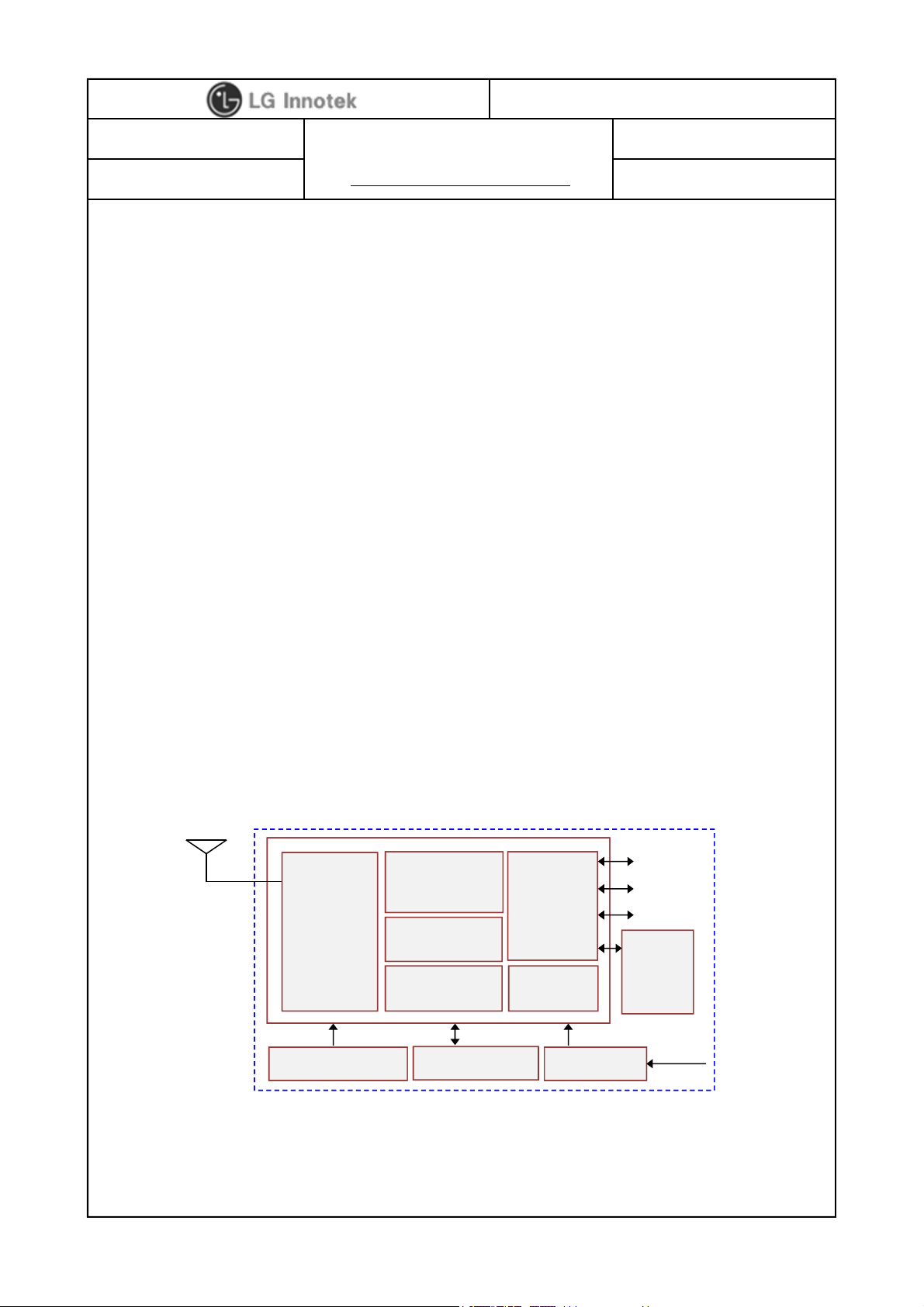
2. Block Diagram
ANT
802.11n
WLAN
MAC/BB
Clock(40MHz)
QCA4010
CPU
(Xtensa 7)
ROM 1MB
RAM 1.5MB PMU
I2C
Homekit
Interface
Block
3.3V
DC-DC
UART
JTAG
USB
Flash
Memory
(4MB)
5V,12V
©2015 LGIT. All rights reserved.
Page 4
REG. DATE : 2015. 09. 10
Specification For Approval
REV. NO : 1 0
REV. DATE : 2015. 09. 10
MODEL NAME : LCW-003
PAGE :
3/ 14
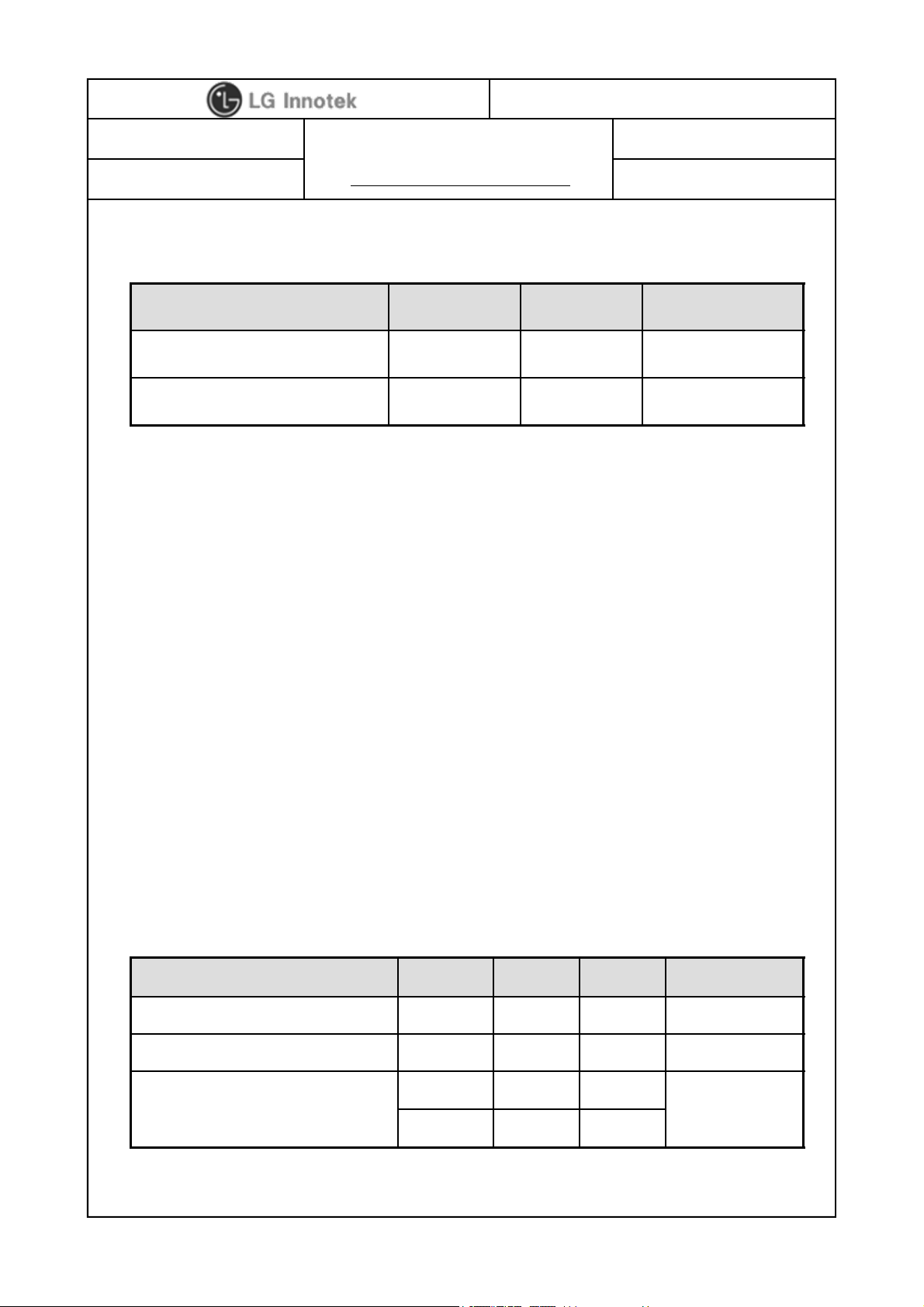
3. Storage conditions
Parameter Min Max Unit
Storage Temperature -20 +80
Storage Humidity (@ 40℃)
Caution : The specifications above the Table define levels at which permanent damage
to the device can occur. Function operation is not guaranteed under these conditions.
Operating at absolute maximum conditions for extend periods can adversely affect the
long-term reliability of the device.
• Other conditions
-90 %
℃
1) Do not use or store modules in the corrosive atmosphere, especially where chloride
gas, sulfide gas, acid, alkali, salt or the like are contained.
Also, avoid exposure to moisture.
2) Store the modules where the temperature
and relative humidity do not exceed 5 to 40℃ and 20 to 60%.
3) Assemble the modules within 6 months.
Check the soldering ability in case of 6 months over.
4. Operating Test Conditions
Parameter Min Typ Max Unit
Operating Temperature 0 - +60
Operating Humidity (40℃)
Supply Voltage
--85 %
4.5 5.0 5.5
10.8 12 13.2
℃
dc
V
©2015 LGIT. All rights reserved.
Page 5
REG. DATE : 2015. 09. 10
Specification For Approval
REV. NO : 1 0
REV. DATE : 2015. 09. 10
MODEL NAME : LCW-003
PAGE :
4/ 14
5. Electrical Characteristics
5-1. RF Characteristics for IEEE802.11b (11Mbps mode unless otherwise specified)
Items Contents
Specification IEEE802.11b
Mode DSSS/CCK
Channel frequency 2400 ~ 2483 MHz
Data rate 1,2,5.5,11Mbps
TX Characteristics Min. Typ. Max. Unit
Power Level 13 17 21 dBm
Spectrum Mask
st
side lobes ( to fc ±11MHz)
1
nd
side lobes ( to fc ±22MHz)
2
--43-30dBr
--58-50dBr
Modulation Accuracy (EVM) - 30 35 %
Power On/Off ramp - 0.5 2.0 Usec
Freq. Tolerance -25 - 25 ppm
Chip Clock Freq. Tolerance -25 - 25 ppm
RX Characteristics Min. Typ. Max. Unit
Minimum Input Level Sens. (FER ≤ 8%) -88 -76 dBm
Maximum Input Level (FER ≤ 8%) -10 - - dBm
* Normal Condition : 25℃, VDD=5V.
* RF characteristics is board limit. It can differ according to standards
©2015 LGIT. All rights reserved.
Page 6

REG. DATE : 2015. 09. 10
Specification For Approval
REV. NO : 1 0
REV. DATE : 2015. 09. 10
MODEL NAME : LCW-003
PAGE :
5/ 14
5-2. RF Characteristics for IEEE802.11g (54Mbps mode unless otherwise specified)
Items Contents
Specification IEEE802.11g
Mode OFDM
Channel frequency 2400 ~ 2483 MHz
Data rate 6,9,12,18,24,36,48,54Mbps
TX Characteristics Min. Typ. Max. Unit
Power Level 10 14 18 dBm
Spectrum Mask
at fc ±11MHz
at fc ±20MHz
at fc ≥ ± 30MHz
--32-20dBr
--43-28dBr
--48-40dBr
Constellation Error (EVM) - -32 -25 dB
Freq. Tolerance -20 - 20 ppm
Chip Clock Freq. Tolerance -20 - 20 ppm
RX Characteristics Min. Typ. Max. Unit
Minimum Input Level Sens. (PER ≤ 10%) - -73 -65 dBm
Maximum Input Level (PER ≤ 10%) -20 - - dBm
* Normal Condition : 25℃, VDD=5V.
* RF characteristics is board limit. It can differ according to standards
©2015 LGIT. All rights reserved.
Page 7

REG. DATE : 2015. 09. 10
Specification For Approval
REV. NO : 1 0
REV. DATE : 2015. 09. 10
MODEL NAME : LCW-003
PAGE :
6/ 14
5-3. RF Characteristics for IEEE802.11gn (MCS7 mode unless otherwise specified)
Items Contents
Specification IEEE802.11n – 2.4GHz
Mode OFDM
Channel frequency 2400 ~ 2483 MHz
Data rate 6.5,13,19.5,26,39,52,58.5,65Mbps
TX Characteristics Min. Typ. Max. Unit
Power Level (HT20 : MCS7) 9 13 17 dBm
Spectrum Mask (HT20)
at fc ±11MHz
at fc ±20MHz
at fc ±30MHz
--32-20dBr
--35-28dBr
--45-40dBr
Constellation Error (EVM) - -32 -28 dB
Freq. Tolerance -20 - 20 ppm
Chip Clock Freq. Tolerance -20 - 20 ppm
RX Characteristics Min. Typ. Max. Unit
Minimum Input Level Sens.
(HT20,PER ≤ 10%)
--68-64dBm
Maximum Input Level (PER ≤ 10%) -20 - - dBm
* Normal Condition : 25℃, VDD=5V.
* RF characteristics is board limit. It can differ according to standards
©2015 LGIT. All rights reserved.
Page 8

REG. DATE : 2015. 09. 10
Specification For Approval
REV. NO : 1 0
REV. DATE : 2015. 09. 10
6. Pin Description
Pin No. Pin Name I/O Pin Description
1VDDI
2 UART Rx I UART Communication signal line
3 UART Tx O UART Communication signal line
4 GND - GND
< TOP View > < Bottom View >
MODEL NAME : LCW-003
VDD 5.0V, 12V ±5%
PAGE :
7/ 14
4
1
Note.
1) Recommend a Module install sequence for prevent UART device failure
- Supply 5.0V, 12V power
- Connect to data signal (UART Tx, UART Rx)
2) Connector: 4Pin SMD Connector
©2015 LGIT. All rights reserved.
A
Page 9

REG. DATE : 2015. 09. 10
Specification For Approval
REV. NO : 1 0
REV. DATE : 2015. 09. 10
7. Outline Drawing
MODEL NAME : LCW-003
PAGE :
8/ 14
©2015 LGIT. All rights reserved.
Page 10

REG. DATE : 2015. 09. 10
Specification For Approval
REV. NO : 1 0
REV. DATE : 2015. 09. 10
8. Packing Information
MODEL NAME : LCW-003
PAGE :
9/ 14
©2015 LGIT. All rights reserved.
Page 11

REG. DATE : 2015. 09. 10
Specification For Approval
REV. NO : 1 0
REV. DATE : 2015. 09. 10
MODEL NAME : LCW-003
PAGE :
10 / 14
9. Warning Statement
<FCC Warning Statements>
FCC Part 15.19 Statements:
This device complies with Part 15 of the FCC Rules. Operation is subject to the
following two conditions: (1) this device may not cause harmful interference, and
(2) this device must accept any interference received, including interference that
may cause undesired operation.
FCC Part 15.105 statement
This equipment has been tested and found to comply with the limits for a Class
B digital device, pursuant to part 15 of the FCC Rules.
These limits are designed to provide reasonable protection against harmful
interference in a residential installation. This equipment generates, uses and can
radiate radio frequency energy and, if not installed and used in accordance with
the instructions, may cause harmful interference to radio communications.
However, there is no guarantee that interference will not occur in a particular
installation. If this equipment does cause harmful interference to radio or
television reception, which can be determined by turning the equipment off and
on, the user is encouraged to try to correct the interference by one or more of
the following measures:
- Reorient or relocate the receiving antenna.
- Increase the separation between the equipment and receiver.
- Connect the equipment into an outlet on a circuit different from that to which
the receiver is connected.
- Consult the dealer or an experienced radio/TV technician for help.
FCC Part 15.21 statement
Any changes or modifications not expressly approved by the party responsible
for compliance could void the user's authority to operate this equipment.
©2015 LGIT. All rights reserved.
Page 12

REG. DATE : 2015. 09. 10
Specification For Approval
REV. NO : 1 0
REV. DATE : 2015. 09. 10
MODEL NAME : LCW-003
PAGE :
11 / 14
9. Warning Statement
RF Exposure Statement
The antenna(s) must be installed such that a minimum separation distance of at
least 20 cm is maintained between the radiator (antenna) and all persons at all
times. This device must not be co-located or operating in conjunction with any
other antenna or transmitter.
End Product Labeling
The module is labeled with its own FCC ID and IC Certification Number. If the
FCC ID and IC Certification Number are not visible when the module is installed
inside another device, then the outside of the device into which the module is
installed must also display a label referring to the enclosed module. In that case,
the final end product must be labeled in a visible area with the following:
“Contains FCC ID: BEJ-LCW003”
“Contains IC: 2703N-LCW003”
<IC Warning Statements>
RSS-GEN, Sec. 7.1.3 – (licence-exempt radio apparatus)
This device complies with Industry Canada license-exempt RSS standard(s).
Operation is subject to the following two conditions: (1) this device may not
cause interference, and (2) this device must accept any interference, including
interference that may cause undesired operation of the device.
Le présent appareil est conforme aux CNR d’Industrie Canada applicables aux
appareils radio exempts de licence. L’exploitation est autorisée aux deux
conditions suivantes : (1) l’appareil ne doit pas produire de brouillage, et (2)
l’utilisateur de l’appareil doit accepter tout brouillage radioélectrique subi, même
si le brouillage est susceptible d’en compromettre le fonctionnement.
©2015 LGIT. All rights reserved.
Page 13

REG. DATE : 2015. 09. 10
Specification For Approval
REV. NO : 1 0
REV. DATE : 2015. 09. 10
MODEL NAME : LCW-003
PAGE :
12 / 14
9. Warning Statement
RF Exposure
The antenna (or antennas) must be installed so as to maintain at all times a
distance minimum of at least 20 cm between the radiation source (antenna) and
any individual. This device may not be installed or used in conjunction with any
other antenna or transmitter.
l'exposition aux RF
L’antenne (ou les antennes) doit être installée de façon à maintenir à tout
instant une distance minimum de au moins 20 cm entre la source de radiation
(l’antenne) et toute personne physique.
Caution: Any changes or modifications to this device not explicitly approved by
manufacturer could void your authority to operate this equipment.
Attention: Les changements ou modifications de cet appareil non expressément
approuvé par le fabricant peuvent annuler votre droit à utiliser cet équipement.
Étiquetage du produit final (IC)
Le module BT111 est étiqueté avec sa propre identification FCC et son propre
numéro de
certification IC. Si l’identification FCC et le numéro de certification IC ne sont
pas visibles lorsque
le module est installé à l’intérieur d’un autre dispositif, la partie externe du
dispositif dans lequel
le module est installé devra également présenter une étiquette faisant référence
au module inclus.
Dans ce cas, le produit final devra être étiqueté sur une zone visible avec les
informations
©2015 LGIT. All rights reserved.
Page 14

REG. DATE : 2015. 09. 10
Specification For Approval
REV. NO : 1 0
REV. DATE : 2015. 09. 10
MODEL NAME : LCW-003
PAGE :
13 / 14
9. Warning Statement
suivantes :
« Contient module émetteur identification FCC ID : BEJ-LCW003
« Contient module émetteur IC : 2703N-LCW003”
The OEM integrator has to be aware not to provide information to the end user
regarding how to install or remove this RF module or change RF related
parameters in the user manual of the end product.
OEM Responsibilities to comply with FCC and Industry Canada
Regulations
The module has been certified for integration into products only by OEM
integrators under the following condition:
- The transmitter module must not be co-located or operating in conjunction with
any other antenna or transmitter except in accordance with FCC multi-
transmitter product procedures.
As long as the two condition above is met, further transmitter testing will not be
required.
However, the OEM integrator is still responsible for testing their end-product for
any additional compliance requirements required with this module installed (for
example, digital device emissions, PC peripheral requirements, etc.).
IMPORTANT NOTE: In the event that these conditions can’t be met (for certain
configurations or co-location with another transmitter), then the FCC and
Industry Canada authorizations are no longer considered valid and the FCC ID
and IC Certification Number can’t be used on the final product. In these
circumstances, the OEM integrator will be responsible for re-evaluating the end
product (including the transmitter) and obtaining a separate FCC and Industry
Canada authorization.
©2015 LGIT. All rights reserved.
Page 15

REG. DATE : 2015. 09. 10
Specification For Approval
REV. NO : 1 0
REV. DATE : 2015. 09. 10
MODEL NAME : LCW-003
PAGE :
14 / 14
9. Warning Statement
Responsabilités des OEM quant à la conformité avec les réglementations
de FCC et d’ Industrie Canada
Les modules ont été certifiés pour entrer dans la fabrication de produits
exclusivement réalisés par des intégrateurs dans les conditions suivantes :
- Le module transmetteur ne doit pas être installé ou utilisé en concomitance
avec une autre antenne ou un autre transmetteur.
Tant que ces deux conditions sont réunies, il n’est pas nécessaire de procéder à
des tests
supplémentaires sur le transmetteur. Cependant, l’intégrateur est responsable
des tests effectués sur le produit final afin de se mettre en conformité avec
d’éventuelles exigences complémentaires lorsque le module est installé
(exemple : émissions provenant d’appareils
numériques, exigences vis-à-vis de périphériques informatiques, etc.)
REMARQUE IMPORTANTE : En cas d’inobservance de ces conditions (en ce
qui concerne
certaines configurations ou l’emplacement du dispositif à proximité d’un autre
émetteur), les
autorisations de FCC et d’Industrie Canada ne seront plus considérées valables
et l’identification de FCC et le numéro de certification d’IC ne pourront pas être
utilisés sur le produit final. Dans ces cas, l’intégrateur OEM sera chargé
d’évaluer à nouveau le produit final (y compris l’émetteur) et d’obtenir une
autorisation indépendante de FCC et d’Industrie Canada.
- Dans le guide d’utilisation du produit final, l’intégrateur OEM doit s’abstenir de
fournir des informations à l’utilisateur final portant sur les procédures à suivre
pour installer ou retirer ce module RF ou pour changer les paramètres RF.
©2015 LGIT. All rights reserved.
 Loading...