

Page 1

SERVICE MANUAL
SERVICE MANUAL
CAUTION
BEFORE SERVICING THE UNIT, READ THE “SAFETY PRECAUTIONS”
IN THIS MANUAL.
Internal Use Only
Website http://biz.lgservice.com
JULY, 2015
MODEL: LAS350B (LAS350B, S35A1-W)
MODEL: LAS350B
(LAS350B, S35A1-W)
Sound Bar
P/NO : AFN77277006
Page 2

CONTENTS
SECTION 1 ........ GENERAL
SECTION 2 ........ CABINET & MAIN CHASSIS
SECTION 3 ........ ELECTRICAL
SECTION 4 ........ REPLACEMENT PARTS LIST
1-1
Page 3

SECTION 1
GENERAL
CONTENTS
ESD PRECAUTIONS ......................................................................................................................................... 1-3
HIDDEN KEY MODE ......................................................................................................................................... 1-4
SERVICE INFORMATION FOR EEPROM ........................................................................................................ 1-4
MCS / EQ HIDDEN KEY GUIDE ....................................................................................................................... 1-5
MCS / EQ PROGRAM UPDATE GUIDE ........................................................................................................... 1-5
SPECIFICATIONS ............................................................................................................................................. 1-6
1-2
Page 4
ESD PRECAUTIONS
Electrostatically Sensitive Devices (ESD)
Some semiconductor (solid state) devices can be damaged easily by static electricity. Such components
commonly are called Electrostatically Sensitive Devices (ESD). Examples of typical ESD devices are integrated
circuits and some field-effect transistors and semiconductor chip components. The following techniques should
be used to help reduce the incidence of component damage caused by static electricity.
1. Immediately before handling any semiconductor component or semiconductor-equipped assembly, drain off
any electrostatic charge on your body by touching a known earth ground. Alternatively, obtain and wear a
commercially available discharging wrist strap device, which should be removed for potential shock reasons
prior to applying power to the unit under test.
2. After removing an electrical assembly equipped with ESD devices, place the assembly on a conductive surface
such as aluminum foil, to prevent electrostatic charge buildup or exposure of the assembly.
3. Use only a grounded-tip soldering iron to solder or unsolder ESD devices.
4. Use only an anti-static solder removal device. Some solder removal devices not classified as "anti-static" can
generate electrical charges sufficient to damage ESD devices.
5. Do not use freon-propelled chemicals. These can generate electrical charges sufficient to damage ESD
devices.
6. Do not remove a replacement ESD device from its protective package until immediately before you are
ready to install it. (Most replacement ESD devices are packaged with leads electrically shorted together by
conductive foam, aluminum foil or comparable conductive materials).
7. Immediately before removing the protective material from the leads of a replacement ESD device, touch the
protective material to the chassis or circuit assembly into which the device will by installed.
CAUTION : BE SURE NO POWER IS APPLIED TO THE CHASSIS OR CIRCUIT, AND OBSERVE ALL OTHER
SAFETY PRECAUTIONS.
8. Minimize bodily motions when handing unpackaged replacement ESD devices. (Otherwise harmless motion
such as the brushing together of your clothes fabric or the lifting of your foot from a carpeted floor can generate
static electricity sufficient to damage an ESD device).
CAUTION. GRAPHIC SYMBOLS
THE LIGHTNING FLASH WITH APROWHEAD SYMBOL. WITHIN AN EQUILATERAL TRIANGLE, IS
INTENDED TO ALERT THE SERVICE PERSONNEL TO THE PRESENCE OF UNINSULATED
“DANGEROUS VOLTAGE” THAT MAY BE OF SUFFICIENT MAGNITUDE TO CONSTITUTE A RISK OF
ELECTRIC SHOCK.
THE EXCLAMATION POINT WITHIN AN EQUILATERAL TRIANGLE IS INTENDED TO ALERT THE
SERVICE PERSONNEL TO THE PRESENCE OF IMPORTANT SAFETY INFORMATION IN SERVICE
LITERATURE.
1-3
Page 5
HIDDEN KEY MODE
HIDDEN MODE KEYS
USB MODE ENTRY/UPDATE Main set ‘-’ (Volume) + Remote control ‘MUTE’
EEPROM EDIT Main set ‘-’ (Volume) + Remote control ‘OPTICAL’
EEPROM CLEAR (Initialize) Main set ‘-’ (Volume) + Remote control ‘Treble/Bass’
VERSION CHECK Main set ‘-’ (Volume) + Remote control ‘LG TV’
up Sound Effect
down NIGHT
right F.Skip (Right)
left B.Skip (Left)
enter AV Sync
SERVICE INFORMATION FOR EEPROM
POWER ON
OPT Status
Main set ‘-’ (Volume) + Remote control ‘OPTICAL’
VFD " OPT.."
Use arrow key [Sound Effect, NIGHT, F.Skip (Right), B.Skip (Left)] to move to appropriate position and make changes
Remote control ‘AV SYNC’
Display VFD “E2P CLR”
Power off automatically
Power cord unplug
1-4
Page 6

MCS / EQ HIDDEN KEY GUIDE
1. Version & Option Check
1) Power on.
2) Press main set “-” (volume -) key and remote control "LG TV" key during 3 seconds.
3) Check MCS version.
Ex) P1412120
4) Press remote control “F.Skip (Right)” 1 time.
Check EQ version.
Ex) Q1412020
5) Press remote control “F.Skip (Right)” 1 time.
Check option.
Ex) 10010000
2. Initialize
1) Power on.
2) Press main set “-” (volume -) key and remote control “Treble/Bass” during 3 seconds.
3) Display VFD “E2P CLR”.
4) Power off automatically.
5) Power cord unplug.
MCS / EQ PROGRAM UPDATE GUIDE
1. Preparation
- Remote control.
- Do format USB Memory to FAT32 File system.
- USB : Update fi le exist only in the USB Memory stick.
Ex ) LAS350B :
MCS E:₩LAS350B_FW_201412221.bin (if USB driver is E:₩)
EQ E:₩EQ_PRG_LAS350B_141219_0_4112.bin (if USB driver is E:₩)
2. Update
1) Power on.
2) Change the USB function. [Main set ‘-’ (Volume) + Remote control ‘MUTE’]
3) Insert USB.
4) Display in VFD.
MCS : “MCS UP” “FINISH” Power off.
EQ : “EQ UP” “FINISH” Power off.
5) Loading is shown while updating.
Never remove USB or AC cord.
6) After update fi nish, show FINISH in VFD and power of automatically.
7) Power cord un-plug.
1-5
Page 7

SPECIFICATIONS
• GENERAL
Power requirements Refer to the main label on the unit.
Power consumption Refer to the main label on the unit.
Networked standby : 0.5 W
(If all network ports are activated.)
Dimensions (W x H x D) 880 mm x 59 mm x 90 mm
Net Weight (Approx.) 1.9 kg
Operating temperature 5 °C to 35 °C
Operating humidity 5 % to 90 %
• INPUT/OUTPUT
OPT. IN 3 V (p-p), Optical jack x 1
PORT. IN 0.5 Vrms (3.5 mm stereo jack) x 1
Available Digital Input Audio
Sampling Frequency 32 kHz, 44.1 kHz, 48 kHz, 96 kHz
• AMPLIFIER
Total 120 W
Front 25 W x 2 (6 Ω at 1 kHz)
Subwoofer 70 W (4 Ω at 100 Hz)
THD 10 %
• SUBWOOFER (S35A1-W)
Type 1 Way 1 Speaker
Impedance 4 Ω
Rated Input Power 70 W
Max. Input Power 140 W
Dimensions (W x H x D) 156 mm x 300 mm x 288 mm
Net Weight (Approx.) 2.9 kg
• BLUETOOTH
Codec SBC
• Designs and specifications are subject to change without prior notice.
1-6
Page 8

SECTION 2
CABINET & MAIN CHASSIS
CONTENTS
EXPLODED VIEWS ........................................................................................................................................... 2-3
1. MAIN SET SECTION ................................................................................................................................ 2-3
2. SUBWOOFER SECTION .......................................................................................................................... 2-5
3. PACKING ACCESSORY SECTION ......................................................................................................... 2-7
2-1
Page 9

2-2
Page 10
D
C
503
251
A42
262
B/T
KEY
CABLE5
CABLE6
CABLE7
CABLE3
CABLE8
CABLE7
CABLE6
506
257
A53
258
A54
258
504
257
506
A45
504
503
503
263
506
266
504
504
505
259
A52
264
504
K
USB
DISPLAY
MAIN
SMPS
B
I
G
H
A
B
E
F
H
C
D
F
G
E
J
J
A
K
I
CABLE2
CABLE1
CABLE4
A47
505
504
A43
A46
505
505
A48
A55
265
256
256
300
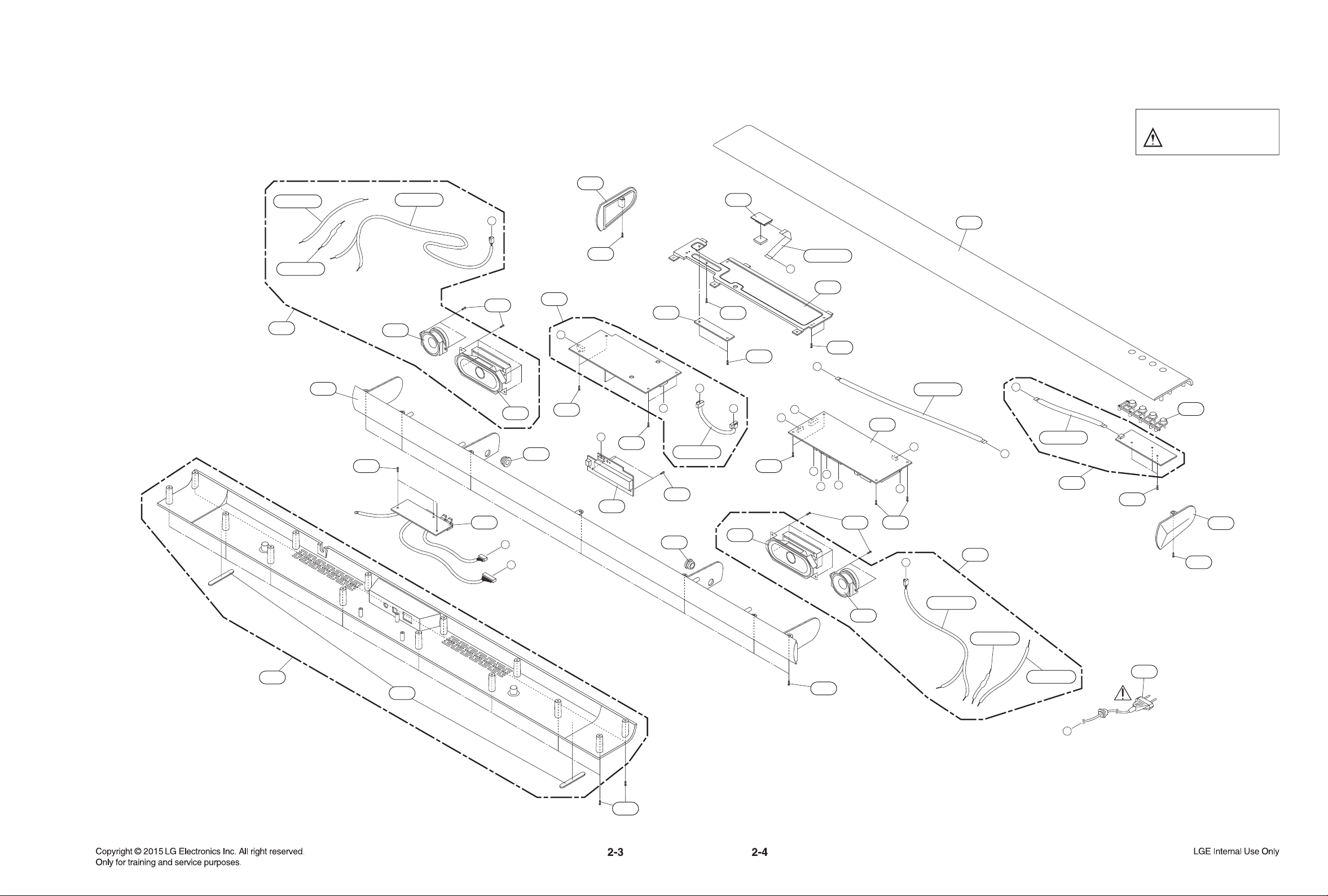
EXPLODED VIEWS
1. MAIN SET SECTION
NOTES) THE EXCLAMATION POINT WITHIN AN
EQUILATERAL TRIANGLE IS INTENDED
TO ALERT THE SERVICE PERSONNEL
TO THE PRESENCE OF IMPORTANT
SAFETY INFORMATION IN SERVICE
LITERATURE.
Page 11
2. SUBWOOFER SECTION
A900
Page 12
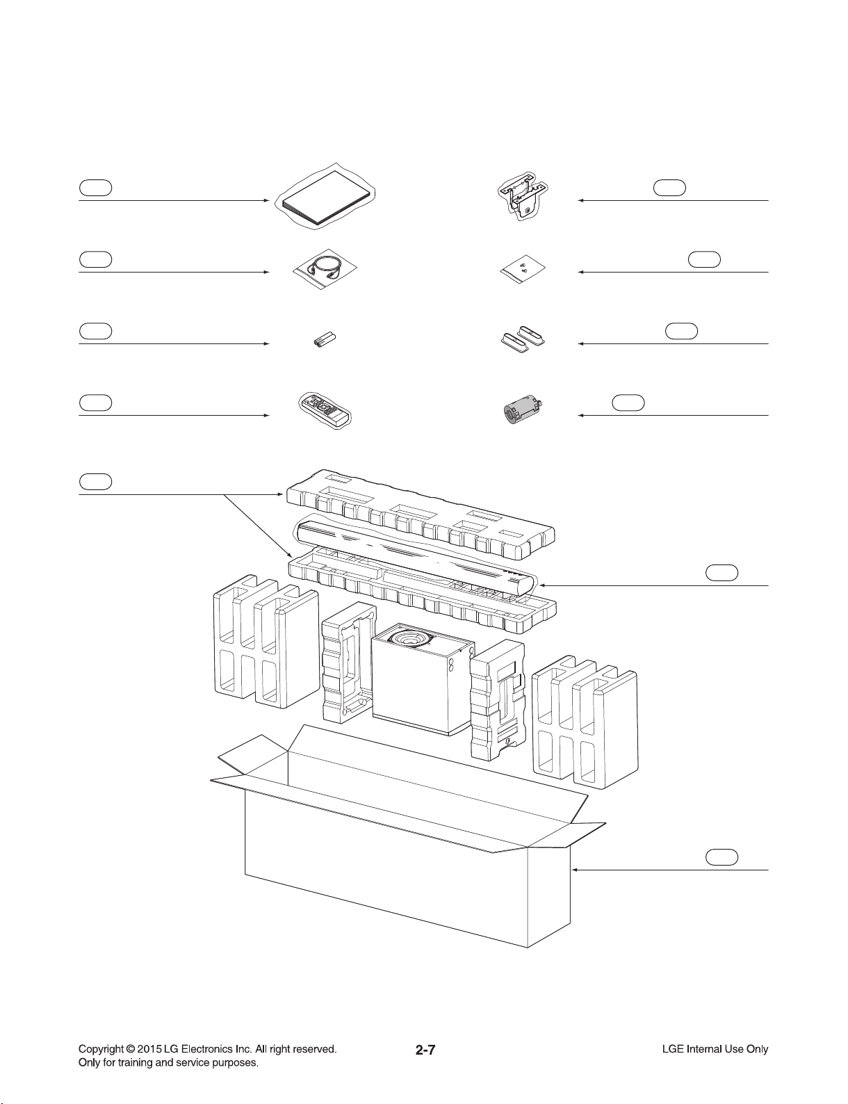
3. PACKING ACCESSORY SECTION
801 Owner’s manual 835 Wall bracket
806 Optical cable 836 Screws
808 Batteries 837 Cover foot
900 Remote control 826 Filter, Ferrite Core
803 Packing, Main
804 Bag
802 Box
Page 13

2-8
Page 14

SECTION 3
ELECTRICAL
CONTENTS
ONE POINT REPAIR GUIDE ............................................................................................................................ 3-2
1. NO POWER PROBLEM (PVDD) ............................................................................................................ 3-2
2. POWER ON ERROR .............................................................................................................................. 3-3
3. NO SOUND (PORTABLE FUNCTION) .................................................................................................. 3-4
4. NO BLUETOOTH .................................................................................................................................... 3-5
5. NO SOUND (OPTICAL) .......................................................................................................................... 3-6
ELECTRICAL TROUBLESHOOTING GUIDE ................................................................................................... 3-7
1. POWER SUPPLY CIRCUIT .................................................................................................................... 3-7
2. FRONT CIRCUIT .................................................................................................................................... 3-8
3. TEST & DEBUG FLOW ........................................................................................................................ 3-10
4. AMP PROTECTION .............................................................................................................................. 3-13
WAVEFORMS OF MAJOR CHECK POINT .................................................................................................... 3-14
1. CRYSTAL .............................................................................................................................................. 3-14
2. FLASH MEMORY ................................................................................................................................. 3-15
3. TACT KEY ............................................................................................................................................. 3-16
4. USB ....................................................................................................................................................... 3-17
5. REMOTE CONTROL ............................................................................................................................ 3-18
6. OPTICAL ............................................................................................................................................... 3-19
7. PORTABLE ........................................................................................................................................... 3-20
8. AUDIO PWM ......................................................................................................................................... 3-21
9. AUDIO AMP .......................................................................................................................................... 3-23
WIRING DIAGRAM .......................................................................................................................................... 3-25
BLOCK DIAGRAM .......................................................................................................................................... 3-27
CIRCUIT DIAGRAMS ...................................................................................................................................... 3-29
1. SMPS CIRCUIT DIAGRAM .................................................................................................................. 3-29
2. MAIN - DSP CIRCUIT DIAGRAM ......................................................................................................... 3-31
3. MAIN - POWER CIRCUIT DIAGRAM ................................................................................................... 3-33
4. MAIN - PWM & AMP CIRCUIT DIAGRAM ........................................................................................... 3-35
5. DISPLAY/ KEY/ USB CIRCUIT DIAGRAM ........................................................................................... 3-37
CIRCUIT VOLTAGE CHART ........................................................................................................................... 3-39
PRINTED CIRCUIT BOARD DIAGRAMS ....................................................................................................... 3-41
1. SMPS P. C. BOARD DIAGRAM ........................................................................................................... 3-41
2. MAIN P. C. BOARD DIAGRAM ............................................................................................................ 3-43
3. DISPLAY P. C. BOARD DIAGRAM ...................................................................................................... 3-45
4. KEY P. C. BOARD DIAGRAM .............................................................................................................. 3-45
5. USB P. C. BOARD DIAGRAM .............................................................................................................. 3-45
3-1
Page 15
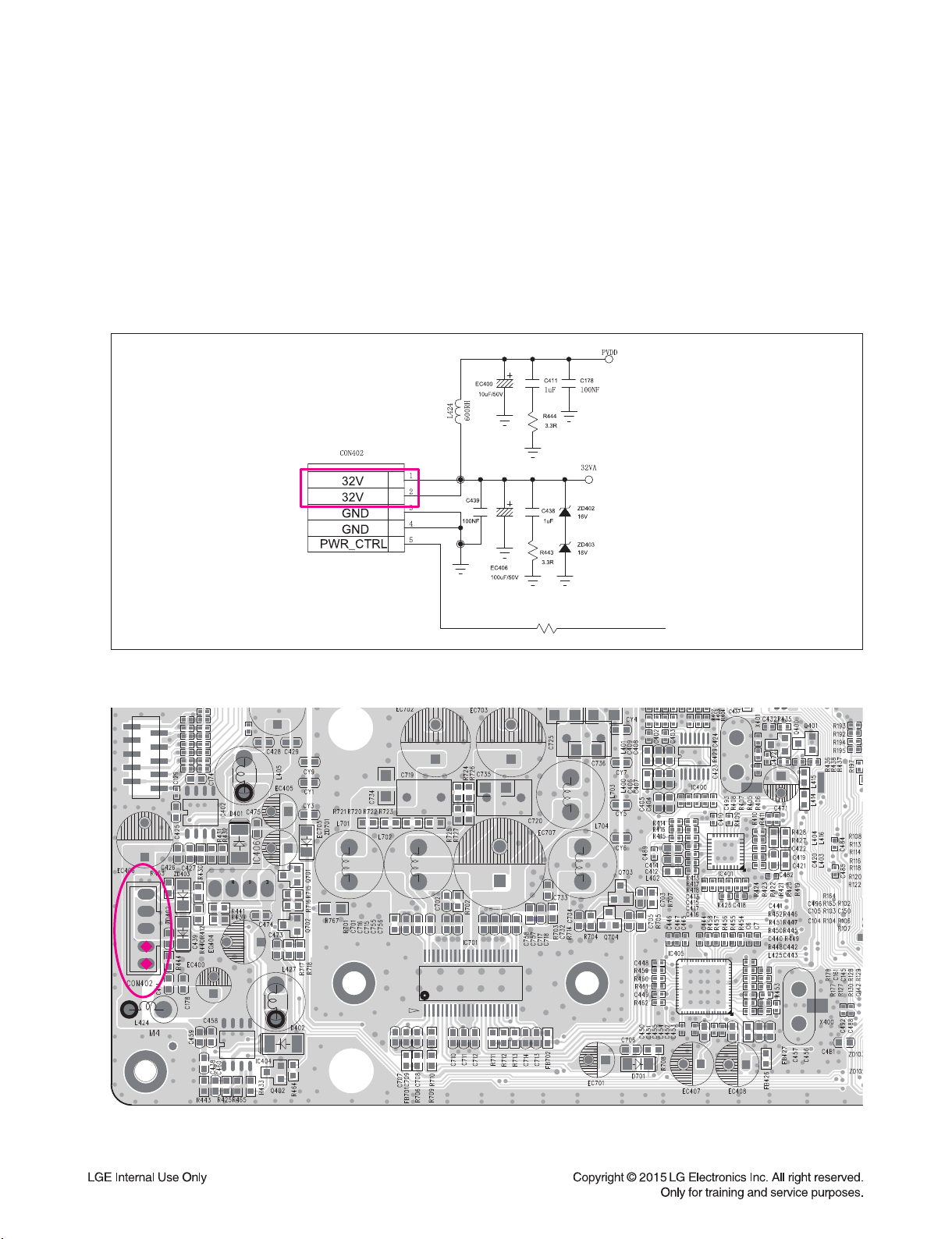
ONE POINT REPAIR GUIDE
CON402 pin1, 2
1. NO POWER PROBLEM (PVDD)
No power problem occurs when you power on the unit
1-1. Solution
Replace SMPS board.
1-2. How to troubleshoot (Countermeasure)
1) Check the PVDD voltage 32 V at pin1, 2.
When you check the no power at this point, then replace SMPS board.
1-3. Service hint (Any picture / Remark)
CON402 pin1, 2
R463
1K
< MAIN board top view >
3-2
Page 16

ONE POINT REPAIR GUIDE
L405
L427
EC405
IC402 pin1
IC404 pin1
IC406 pin E
2. POWER ON ERROR
No display or Not working.
2-1. IC402
1) Check 3.3 VA at L405.
2) If 3.3 VA is not checked at the point, then find 32 V at pin1 of IC402.
3) 1), 2) is NG. Replace IC402.
L405
IC402 pin1
< MAIN board top view >
2-2. IC404
1) Check 12 VA at L427.
2) If 12 VA is not checked at the point, then find 32 V at pin1 of IC404.
3) 1), 2) is NG. Replace IC404.
L427
IC404 pin1
< MAIN board top view >
2-3. IC406
1) Check 5 VA at EC405.
2) If 5 VA is not checked at the point, then find 12 V at pin E of IC406.
3) 1), 2) is NG. Replace IC406.
EC405
IC406 pin E
< MAIN board top view >
3-3
Page 17

ONE POINT REPAIR GUIDE
JK504
L501
L502
IC400
3. NO SOUND (PORTABLE FUNCTION)
3-1. Solution
Replace IC400 or portable jack (JK504).
3-2. How to troubleshoot (Countermeasure)
1) Please check the soldering status of JK504
2) Please check L501, L502 (PORT_L, PORT_R signal) of portable jack (JK504).
If you cannot find input signal, replace JK504.
3) If you can find input signal, check pin13, 14 of IC400.
4) If you can’t find signal at pin13, 14 of IC400, replace IC400.
3-3. Service hint (Any picture / Remark)
JK504
L501
L502
< USB board bottom view >
IC400
< MAIN board top view >
3-4
Page 18

ONE POINT REPAIR GUIDE
IC101
C174
CON102
4. NO BLUETOOTH
4-1. Solution
Replace IC101 on MAIN board.(No 3.3 V)
4-2. How to troubleshoot (Countermeasure)
1)
Please check externally status of Bluetooth cable connection on your eyes.(at CON102 and Bluetooth module)
2) Please check 3.3 V of 3.3VA (at C174).
If 3.3 V is OK at L509, please check BT_SDA, BT_SCL, BT_RST (pin53, 51, 25) of IC101
and BT_RX, BT_TX (pin29, 27).
If you have no signal, please replace IC101.
4-3. Service hint (Any picture / Remark)
CON102
C174
IC101
< MAIN board top view >
3-5
Page 19

ONE POINT REPAIR GUIDE
L505
R428
IC401
5. NO SOUND (OPTICAL)
5-1. Solution
Replace IC401 on MAIN board.
5-2. How to troubleshoot (Countermeasure)
1) Please check 3.3 V of 3.3 VA at L505 in USB board
If you can check 3.3 V, please confirm OPT_DET signal (R428) in MAIN board when optical mode.
2) In spite of process 1), set has abnormal output, then replace IC401.
9
8
4
R
5
L
7
6
123
R317
JK504
0R
100PF
R316
NC
1
OUT
2
GND
3
VCC
JK502
CON502
P_R
P_L
P_DET
P_GND
SPDIF
GND
5V
D+
DGND
L501
600RH
L502
600RH
L503
600RH
L504
3
D503
1
2
3
4
5
6
7
8
R504
9
0R
10
KDS226
1
2
R503
0R
L506
0R
L507
0R
600RH
100PF
C501
100PF
C502
600RH
C503
R318
100R
C317
C505
C506
10PF
100PF
100NF
C316
10NF
C504
100R
L505
L508
600RH
5-3. Service hint (Any picture / Remark)
< USB board bottom view >
L505
IC401
R428
< MAIN board top view >
3-6
Page 20

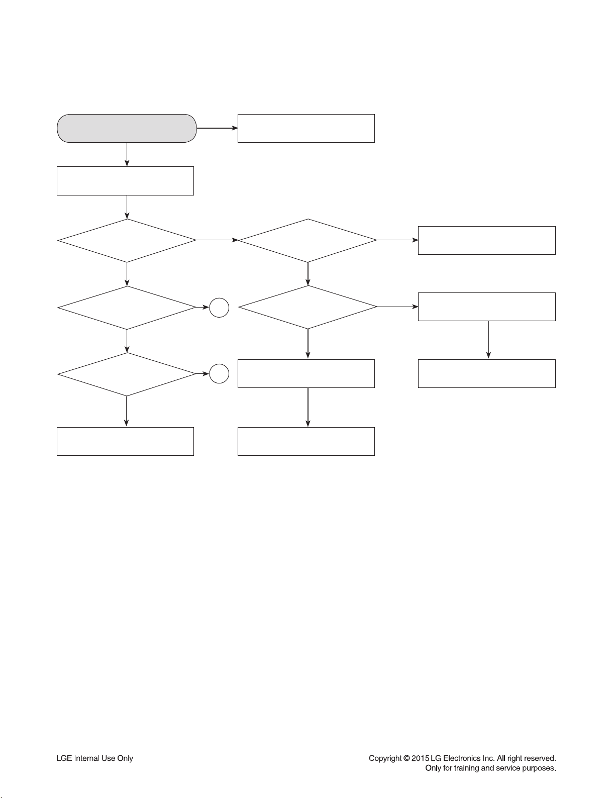
ELECTRICAL TROUBLESHOOTING GUIDE
1. POWER SUPPLY CIRCUIT
INSERT POWER CORD.
Standby LED is normal?
YES
Power on.
YES
Is power on?
YES
Does it output audio?
YES
OK
NO
NO
NO
Check power supply circuit.
Check circuit.
Check audio circuit.
3-7
Page 21
ELECTRICAL TROUBLESHOOTING GUIDE
2. FRONT CIRCUIT
Is the Digitron on correctly?
YES
POWER ON.
YES
LED DISPLAY
correctly?
YES
Check if all
buttons are ok?
YES YES
Check if the remote
control is ok?
YES
NO
NO
NO
NO
Refer to SMPS part.
Check if
CON301 is ok?
YES
1
2
Check if the front
power is ok?
Check if IC301 is ok?
NO
NO
NO
Reconnect it.
Check power supply circuit.
YES
Refer to SMPS part.
Check pattern and resolderingFront B/D ok.
3-8
Page 22

ELECTRICAL TROUBLESHOOTING GUIDE
FRONT CIRCUIT
1
if the power part of the front
Check
is ok?
YES
Check if CON303 is ok?
YES
Check if R306~R309 ok?
YES
Refer to MICOM circuit.
2
NO
NO
NO
Refer to power(SMPS).
Reconnect it.
Replace R306~R309.
if thepower part of the front
Check
is ok?
YES
Check if the remote
control waveform of CON301
pin3 is ok?
YES
Check if REM
voltage is ok(3.3 V)?
YES
Resolder or Replace IR301.
NO
NO
NO
Refer to power(SMPS).
Refer to MICOM circuit.
Check REM circuit
3-9
Page 23

ELECTRICAL TROUBLESHOOTING GUIDE
3. TEST & DEBUG FLOW
TEST.
AC voltage Power PCBA (110 V
Check the
or 220 V).
YES
Switch on the Power PCBA.
YES
Are the
DC Voltage outputs OK? (32 V)
YES
Are 3.3 V and
5 V DC outputs normal on main
PCBA?
YES
Update
FLASH successfully?
NO
NO
NO
NO
Check the POWER PART.
Refer to SMPS part.
Check the POWER PART.
1. Check 24 MHz system clock.
2. Check system reset circuit.
3. Check FLASH R/W enable signal PRD, RWR.
4. Check FLASH Memory related circuit.
YES
A
Replace FLASH.
NO
3-10
Page 24

ELECTRICAL TROUBLESHOOTING GUIDE
A
YES
Power On.
YES
Show HELLO.
YES
Connect a bluetooth device,
music is played.
YES
Does it output
audio?
YES
Show
the bluetooth name
NO
NO
Flash
Memory operates
properly?
YES
SDRAM
works properly?
YES
Check if CON104 is ok?
YES
Check if Front circuit.
Check
if CON102 is ok?
NO
NO
NO
NO
Check connection lines
between FLASH & MCL3730
and the FLASH access time
whether is suitable or not.
Check connection lines
between SDRAM(IC102) &
MCL3730 and the SDRAM
is damaged.
Reconnect it.
Reconnect it.
B
YES
YES
Replace the bluetooth module
NO
Check the AMP part
3-11
Page 25

ELECTRICAL TROUBLESHOOTING GUIDE
B
YES
Function transformation
to OPT
YES
Does it output
audio?
YES
Function transformation
to PORT Insert AUDIO line
YES
Does it output
audio?
YES
NO
NO
Check the OPT
the input signal
YES
Check if JK502
voltage is ok(3.3 V)?
YES
Replace the JK502(OPT)
Check if MCL3730
pin4 “H”
YES
NO
NO
NO
Check the OPT line,
Changing the OPT Equipment
Check if CON502 is ok?
Check if JK504 det.pin
voltage is ok(0 V)?
YES
TEST END.
Check if IC400 pin13, 14
Is there a signal input?
YES
Check if IC400 pin3, 4
voltage is ok(3.3 V, 5 V)?
YES
Check if IC400 pin6~9
(MCLK, LRCK, DATA, BCK)
YES
Replace the IC400
3-12
NO
NO
Replace the JK504
Check the POWER PART.
Page 26

ELECTRICAL TROUBLESHOOTING GUIDE
4. AMP PROTECTION
“S-PROTEC” appears on the FLD.
YES
After unplug power cord, connect again.
YES
Power on.
YES
Display, automatic standby
“Goodbye”
YES
Is the IC701 pin16, 17
“LOW” signal(0 V)?
YES
Is the AMP IC Power
12 V, 32 V normal?
YES
Replace TI AMP IC(IC701, IC702)
NO
NO
NO
OK.
Replace IC701.
12 V: CHECK Q701 Part.
32 V: CHECK SMPS Part.
3-13
Page 27

1. CRYSTAL
1
WAVEFORMS OF MAJOR CHECK POINT
1
FIG 1-1. X101 (24 MHz)
2
2
2
FIG 1-2. X400, X401 (24.576 MHz)
3-14
Page 28

2. FLASH MEMORY
VCC
3
4
4
CS#
CLK
5
DO
6
3
5
6
FIG 2. VCC, CS#, CLK, DO
3-15
Page 29

3. TACT KEY
7 8
1 ~ 1.13 V
FIG 3-1. Press VOL + FIG 3-2. Press VOL -
9
0.72 ~ 0.82 V
10
0.424 ~ 0.485 V
FIG 3-3. Press FUN.KEY
0 V
7 8
9 10
C311
FIG 3-4. Press POWER KEY
3-16
Page 30

4. USB
11
12
FIG 4-1. USB_5V
C475
EC405
100uF/16V
11
13
FIG 4-2. USB D+
12
13
FIG 4-3. USB D-
3-17
Page 31
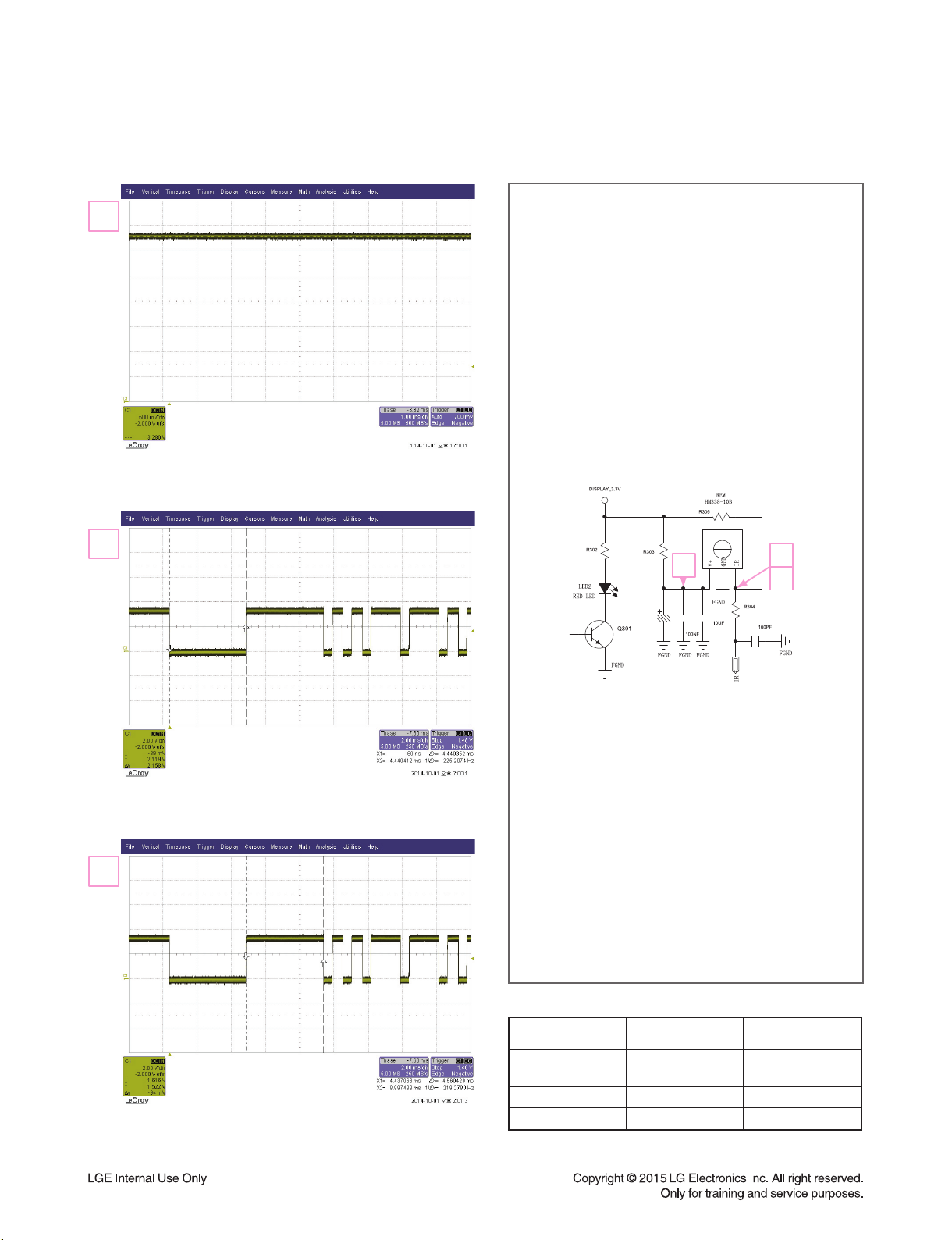
5. REMOTE CONTROL
14
FIG 5-1. Input Voltage
47K
15
16
FIG 5-2. Low Timing
4.7K
100R
14
15
16
EC301
100uF/16V
8050
C301
C304
100R
C302
FIG 5-3. High Timing
3-18
Item Measured Spec.
Input Level 3.3 V
IR Receiver Spec:
2.7 ~ 5.5 V
“ Low” Timing 4.4 ms 3.6 ms ~ 5.04 ms
“ High” Timing 4.48 ms 4.08 ms ~ 5.04 ms
Page 32

6. OPTICAL
17
18
FIG 6-1. OPT_IN
FIG 6-2. OPT_DET
18
17
3-19
Page 33

7. PORTABLE
XUY^G}
19
20
FIG 7-1. ADC IC 5 V
20
19
21
21
FIG 7-2. ADC IC 3.3 V
X
FIG 7-3. Analog Input Voltage
3-20
Page 34

8. AUDIO PWM(1/2)
22 23
FIG 8-1. PWM IC 3.3 V FIG 8-2. PWM IC 1.2 V
24
25
FIG 8-3. BCK
C456
22
C457
25
FB426
600RH
FB427
600RH
24
100R
100R
C454
100R
100R
C452
C453
100R
C444
23
C445
C446
C447
FIG 8-4. LRCK
3-21
Page 35

AUDIO PWM(2/2)
26
FIG 8-5. Front L/R
27
-
384.14 kHz
3R3
C705
1K
1K
26
FB701
600RH
C707
C708
C709
68K
100R
C710
C711
384.17 kHz
FIG 8-6. Subwoofer
27
C712
100R
NC
2.2k
C714
FB702 600RH
C713
3-22
Page 36

9. AUDIO AMP
28
29
30
31
FIG 9-1. AMP IC PVDD: 32 V
PVDD
GVDD
AMP_PDN
FIG 9-2.
C707
C709
100R
C711
FB701
600RH
C708
C710
18R
C715
C716
C717
C718
C701
C702
18R
C732
28
560R
560R
560R
560R
18R
C733
18R
29
330K
C1
C755
C756
C757
C2
C758
30
31
68K
3-23
C712
100R
NC
2.2k
C714
FB702 600RH
C713
Page 37

3-24
Page 38

3-263-25
CON1
AC IN
SMPS
PCB
MAIN
PCB
USB PCB
DISPLAY
PCB
KEY PCB
BT module
F/L SPK
F/R SPK
USBPORTOPT
subwoofer
AC IN
WIRING DIAGRAM
Page 39

3-283-27
Amplifier
TAS5612L
POTABLE IN
Optical in
LED Display
ATA7819Y
LED Driver
SMI616
SMPS
25 W/ 6 Ohm
25 W/ 6 Ohm
SPDIF
R/L
PWM
Tact key
DSP
PS9860
IIS
ADC
PCM1808
Bluetooth
MB8811C1B
70 W/ 4 Ohm
+32 V
DC-DC
IR
USB Port
FLASH
32 M
SDRAM
4 x 16 M
CS8422
FLASH
1M
IIS
IIS
IIC
SPI
SPI
IIC
Main chip IC
MLC3730
BLOCK DIAGRAM
Page 40

3-303-29
A
1
2
3
4
5
6
7
8
9
10
11
12
B C D E F G H I J K L M N O P Q R ST
CAUTION:
Danger if fuse is incorrectly replaced.
Replace only with the type identical to fuse rating
and(or) model name described in main label.
Warning
Parts that are shaded are critical with
respect to risk of fire or electrical shock.
CIRCUIT DIAGRAMS
1. SMPS CIRCUIT DIAGRAM
WHEN SERVICING THIS CHASSIS, UNDER NO
CIRCUMSTANCES SHOULD THE ORIGINAL
DESIGN BE MODIFIED OR ALTERED WITHOUT
PERMISSION FROM THE LG CORPORATION. ALL
COMPONENTS SHOULD BE REPLACED ONLY WITH
TYPES IDENTICAL TO THOSE IN THE ORIGINAL
CIRCUIT. SPECIAL COMPONENTS ARE SHADED
ON THE SCHEMATIC FOR EASY IDENTIFICATION.
THIS CIRCUIT DIAGRAM MAY OCCASIONALLY
DIFFER FROM THE ACTUAL CIRCUIT USED. THIS
WAY, IMPLEMENTATION OF THE LATEST SAFETY
AND PERFORMANCE IMPROVEMENT CHANGES
INTO THE SET IS NOT DELAYED UNTIL THE NEW
SERVICE LITERATURE IS PRINTED.
1. Shaded( ) parts are critical for safety. Replace only
with specified part number.
2. Voltages are DC-measured with a digital voltmeter
during Play mode.
IMPORTANT SAFETY NOTE :
Page 41

3-323-31
12
13
5
6
4
3
7 8
9 10
1
: WAVEFORM NUMBER
A
1
2
3
4
5
6
7
8
9
10
11
12
B C D E F G H I J K L M N O P Q R ST
EC102
100uF/16V
3904
R173
4.7K
R1B1
1K
R1B2
1K
C179
R172
NC
2. MAIN - DSP CIRCUIT DIAGRAM
Page 42

3-343-33
3. MAIN - POWER CIRCUIT DIAGRAM
17
21
11
20
18
2
19
: WAVEFORM NUMBER
A
1
2
3
4
5
6
7
8
9
10
11
12
B C D E F G H I J K L M N O P Q R ST
3904
R435
10K
R436
1K
R437
1K
C471
100uF/16V
C472
R439
10K
R438
10K
R441
20K
EC405
100uF/16V
C475
3904
R463
1K
R464
1K
3904
R716
1K
R717
NC
R715
10K
R718
1K
EC705
100uF/16V
Page 43

3-363-35
29
28
23
22
26
30
27
31
24
25
2
: WAVEFORM NUMBER
A
1
2
3
4
5
6
7
8
9
10
11
12
B C D E F G H I J K L M N O P Q R ST
FB701
600RH
100R
C707
C708
C709
68K
C710
C711
C712
100R
C714
FB702 600RH
C713
3R3
C705
1K
1K
C704
1K
C703
C706
10K
C715
C716
C717
C718
C728
C729
C721
3R3
C723
C724
560R
C727
C730
C726 C731
C755
CY1
NC
2.2k
560R
560R 560R
560R 560R
560R 560R
3R3
4.7K
4.7K
3R3
3R3
C722
C756
C757
C758
330K
CY2
CY3
CY4
CY5
CY6
CY7
CY8
CY9
C732
C733
18R
18R
C701
C702
18R
18R
L425
600RH
FB427
600RH
C457
C456
C440
C441
C444
100R
100R
100R
100R
4.7K
4.7K
4.7K
100R
C445
C446
C447
C448
33R
33R
33R
33R
C449
FB426
600RH
C453
C452
C454
100R
100R
100R
100R
100R
C1
C2
4. MAIN - PWM & AMP CIRCUIT DIAGRAM
Page 44

3-383-37
16
15
14
: WAVEFORM NUMBER
A
1
2
3
4
5
6
7
8
9
10
11
12
B C D E F G H I J K L M N O P Q R ST
FRONT_BOARD
LED
IR
3.3V
SDA
SCL
GND
P_R
P_L
P_DET
P_GND
SPDIF
GND
5V
D+
DGND
KEY
GND
STBY-->H
SW+
SW-
GND
KEY
KEY_BOARD
GND
5V
SW+
SW-
IR
GND
V+
REM
HM338-10B
R305
47K
R304
100R
1
SEG52SEG63SEG74GRID05GRID16GRID27GRID38GRID49SCL10SDA11GND12GRID513GRID614GRID7
15
GRID8
16
GRID9
17
GRID10
18
GRID11
19
GRID12
20
GRID13
21
GRID14
22
GRID15
23
SEGO
24
SEG1
25
VDD
26
SEG227SEG328SEG4
IC301
SM1616
LED2
RED LED
Q301
8050
R303
100R
R302
4.7K
EC301
100uF/16V
C301
100NF
C302
100PF
R301
10K
12
43
SW301
POWER
R306
100R
12
43
SW302
FUN
R307
680R
12
43
SW303
VOL-
R308
1K
12
43
SW304
VOL+
R309
1.5K
1
OUT
2
GND
3
VCC
JK502
4
2
3
1
1:VCC
2:D-
3:D+
4:GND
JK503
USB
L505
600RH
C506
100NF
L504
600RH
L503
600RH
L502
600RH
L501
600RH
L506
0R
L507
0R
L508
600RH
L509
1KRH
C508
NC
C507
10UF
C501
100PF
C502
100PF
C503
100PF
C505
10PF
TP6
1
2
3
D502
NC
1
2
3
D501
NC
1
2
3
D302
NC
1
2
3
D301
NC
R310
10K
R311
10K
R312
100R
R313
100R
EC302
100uF/16V
C305
100NF
1
GRID002GRID013GRID024GRID035SEG006GRID047GRID058SEG019GRID0610GRID0711SEG0212GRID0813GRID0914SEG0315SEG0416GRID1017GRID1118SEG0519SEG0620GRID1221GRID1322SEG0723GRID1424GRID15
LED301
LED_ATA7216AW-P12
1
SPK+
2
SPK-
JK301
C307
100NF
C308
100NF
R
L
123
4
5
6
7
8
9
JK504
1
2
3
4
5
6
7
8
9
10
CON502
1
2
3
4
L510
22UH
R501
0R
R502
0R
R503
0R
R504
0R
C310
10UF
C304
10UF
C306
10UF
C311
100NF
1
2
3
4
CON303
1
2
3
4
5
6
7
CON301
CN/7PIN
C313
100NF
C314
330PF
C315
330PF
R317
0R
R316
NC
1
2
3
4
5
CON302
1
2
3
D503
KDS226
C316
10NF
1
2
3
D300
KDS226
C312
103P
R318
100R
C317
100PF
C504
100R
IR
DISPLAY_3.3V
STB_LED
DISPLAY_3.3V
DISPLAY_SDA
DISPLAY_SCL
FGND
FGND
FGND
FGND FGND
FGND
DISPLAY_3.3V
DISPLAY
5V
FGND
FGND
DISPLAY_SCL
DISPLAY_SDA
FGND
STB_LED
IR
GRD00
SEG00
SEG01
SEG02
SEG03
SEG04SEG05
SEG06
SEG07
GRD00
GRD01
GRD02
GRD03
GRD04
GRD05
GRD06
GRD07 GRD08
GRD09
GRD10
GRD11
GRD12
GRD13
GRD14
GRD15
GRD01
GRD02
GRD03
GRD04
GRD05
GRD06
GRD07
GRD08
GRD09
GRD10
GRD11
GRD12
GRD13
GRD14
GRD15
SEG00
SEG01
SEG02
SEG03
SEG04
SEG05
SEG06
SEG07
FGND FGND
FGND
FGND
FGND
5V
FGND
FGND FGND
DISPLAY_SCL
DISPLAY_SDA
5. DISPLAY/ KEY/ USB CIRCUIT DIAGRAM
Page 45

3-403-39
CIRCUIT VOLTAGE CHART
Designator Description Pin Voltage Spec Measured Voltage
IC101 Digital Signal
Processors
1, 43, 90, 132, 158 3.0~3.6 V 3.28 V
23, 55, 72, 107, 142, 160 1.1~1.3 V 1.19 V
57, 60, 164(USB_VCC) 3.0~3.6 V 3.28 V
66(USB_VCC) 1.1~1.3 V 1.19 V
68(OSC_VCC) 3.0~3.6 V 3.28 V
87(PLL_VCC) 1.1~1.3 V 1.19 V
IC102 SDRAM 1, 3, 9, 14, 27, 43, 49 3.0~3.6 V 3.28 V
IC105 FLASH 8 3.0~3.6 V 3.28 V
IC106 FLASH 8 3.0~3.6 V 3.28 V
IC400 ADC IC
3 4.75~5.25 V 4.98 V
4 3.0~3.6 V 3.28 V
IC401
Digital Audio
Function
19, 22 3.0~3.6 V 3.28 V
IC402 DC TO DC
1 31~33 V 32 V
2 3.0~3.6 V 3.28 V
IC404 DC TO DC
1 31~33 V 32 V
2 11~13 V 11.8 V
IC405 DSP IC
17, 34, 43, 52, 66 3.0~3.6 V 3.28 V
6, 25, 35, 63, 67 1.1~1.3 V 1.2 V
IC406 LDO IC
1 11~13 V 11.8 V
2 4.75~5.25 V 4.98 V
IC701 AMP IC
1, 2, 22 11~13 V 11.8 V
29, 30, 31, 36, 37, 38 31~33 V 32 V
Page 46

3-423-41
PRINTED CIRCUIT BOARD DIAGRAMS
1. SMPS P. C. BOARD DIAGRAM
(TOP VIEW)
(BOTTOM VIEW)
NOTE) Warning
Parts that are critical with respect to risk
of fire or electrical shock.
Page 47

3-443-43
2. MAIN P. C. BOARD DIAGRAM
(TOP VIEW)
(BOTTOM VIEW)
Page 48

3-463-45
3. DISPLAY P. C. BOARD DIAGRAM
5. USB P. C. BOARD DIAGRAM
4. KEY P. C. BOARD DIAGRAM
(TOP VIEW)
(TOP VIEW)
(TOP VIEW)
(BOTTOM VIEW)
(BOTTOM VIEW)
(BOTTOM VIEW)
Page 49

3-483-47
 Loading...