

Page 1
SERVICE MANUAL MODEL : LAC-M8400R
CD/MP3/WMA Player Receiver
Car Stereo
SERVICE MANUAL
CAUTION
BEFORE SERVICING THE UNIT, READ THE “SAFETY PRECAUTIONS”
IN THIS MANUAL.
MODEL : LAC-M8400R
Page 2

- 1-1 -
❍
SECTION 1. SUMMARY
• SERVICING PRECAUTIONS
..........................................................................................................
1-2
• ESD PRECAUTIONS
.......................................................................................................................
1-3
• SPECIFICATIONS
...........................................................................................................................
1-4
❍
SECTION 2. ELECTRICAL
• ELECTRICAL TROUBLESHOOTING GUIDE
.................................................................................
2-1
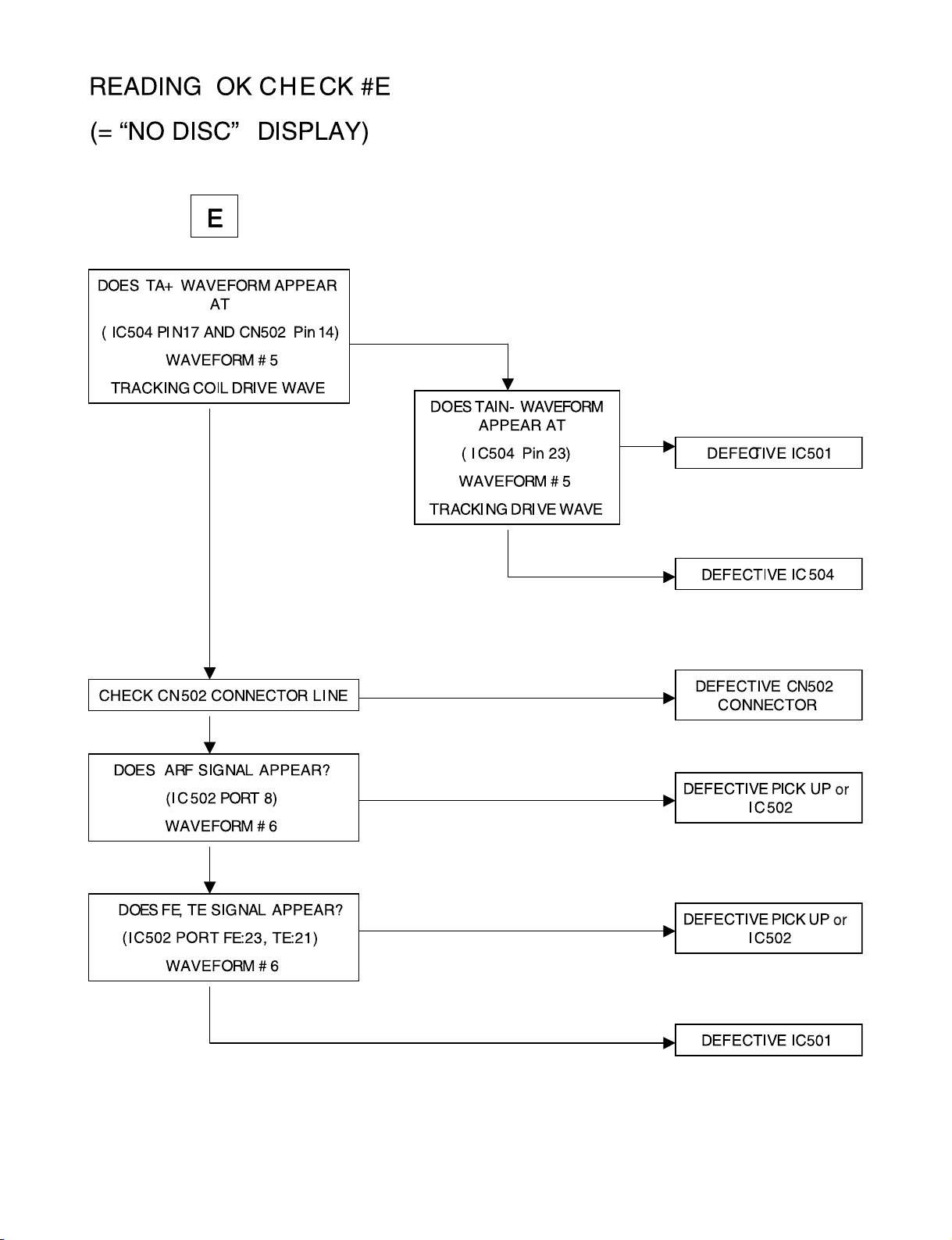
• CD PART TROUBLESHOOTING GUIDE
........................................................................................
2-3
• WAVEFORMS OF MAJOR CHECK POINT
..................................................................................
2-12
• INTERNAL BLOCK DIAGRAM of ICs
............................................................................................
2-14
• BLOCK DIAGRAM
.........................................................................................................................
2-35
- MAIN SCHEMATIC DIAGRAM
...................................................................................................
2-37
- FRONT SCHEMATIC DIAGRAM ............................................................................................... 2-39
- CDP SCHEMATIC DIAGRAM
....................................................................................................
2-41
- H/F & MOTOR SCHEMATIC DIAGRAM
...................................................................................
2-43
• PRINTED CIRCUIT DIAGRAM
......................................................................................................
2-45
❍
SECTION 3. CABINET MAIN CHASSIS & MECHANISM
• EXPLODED VIEW
...........................................................................................................................
3-1
• Accessory part ................................................................................................................................. 3-5
❍
SECTION 4. REPLACEMENT PARTS LIST
....................................................................
4-1
[CONTENTS]
Page 3

-1-2-
❏
SERVICING PRECAUTIONS
➊ Always disconnect the power source before:
1) Removing or reinstalling any component, circuit board, module or any other instrument assembly.
2) Disconnecting or reconnecting any instrument electrical plug or other electrical connection.
3) Connecting a test substitute in parallel with an electrolytic capacitor in the instrument.
CAUTION: A wrong part substitution or incorrect polarity installation of electrolytic capacitors may result in
an explosion hazard.
➋ Do not defeat any plug/socket B+ voltage interlocks with which instruments covered by this service
manual might be equipped.
❸ Do not apply power to this instrument and or any of its electrical assemblies unless all solid-state
device heat sinks are correctly installed.
❹ Always connect a test instrument’s ground lead to the instrument chassis ground before
connecting the test instrument positive lead. Always remove the test instrument ground lead last.
1) The service precautions are indicated or printed on the cabinet, chassis or components. When servicing,
follow the printed or indicated service precautions and service materials.
2) The Components used in the unit have a specified conflammability and dielectric strength. When
replacing any components, use components which have the same ratings. Components marked in
the circuit diagram are important for safety or for the characteristics of the unit. Always replace with the
exact components.
3) An insulation tube or tape is sometimes used and some components are raised above the printed writing
board for safety. The internal wiring is sometimes clamped to prevent contact with heating components.
Install them as they were.
4) After servicing always check that the removed screws, components and wiring have been installed
correctly and that the portion around the service part has not been damaged. Further check the insulation
between the blades of attachment plug and accessible conductive parts.
SECTION 1. SUMMARY
Page 4
- 1-3 -
❏ ESD PRECAUTIONS
Electrostatically Sensitive Devices (ESD)
Some semiconductor (solid state) devices can be damaged easily by static electricity. Such components
commonly are called Electrostatically Sensitive Devices (ESD). Examples of typical ESD devices are integrated
circuits and some field-effect transistors and semiconductor chip components. The following techniques should
be used to help reduce the incidence of component damage caused by static electricity.
1. Immediately before handling any semiconductor component or semiconductor-equipped assembly, drain off
any electrostatic charge on your body by touching a known earth ground. Alternatively, obtain and wear a
commercially available discharging wrist strap device, which should be removed for potential shock reasons
prior to applying power to the unit under test.
2. After removing an electrical assembly equipped with ESD devices, place the assembly on a conductive
surface such as aluminum foil, to prevent electrostatic charge buildup or exposure of the assembly.
3. Use only a grounded-tip soldering iron to solder or unsolder ESD devices.
4. Use only an anti-static solder removal device. Some solder removal devices not classified as "anti-static" can
generate electrical charges sufficient to damage ESD devices.
5. Do not use freon-propelled chemicals. These can generate electrical charges sufficient to damage ESD
devices.
6. Do not remove a replacement ESD device from its protective package until immediately before you are ready
to install it. (Most replacement ESD devices are packaged with leads electrically shorted together by
conductive foam, aluminum foil or comparable conductive materials).
7. Immediately before removing the protective material from the leads of a replacement ESD device, touch the
protective material to the chassis or circuit assembly into which the device will by installed.
CAUTION : BE SURE NO POWER IS APPLIED TO THE CHASSIS OR CIRCUIT, AND OBSERVE ALL OTHER
SAFETY PRECAUTIONS.
8. Minimize bodily motions when handing unpackaged replacement ESD devices. (Otherwise harmless motion
such as the brushing together of your clothes fabric or the lifting of your foot from a carpeted floor can
generate static electricity sufficient to damage an ESD device).
CAUTION. GRAPHIC SYMBOLS
THE LIGHTNING FLASH WITH APROWHEAD SYMBOL. WITHIN AN EQUILATERAL
TRIANGLE, IS INTENDED TO ALERT THE SERVICE PERSONNEL TO THE PRESENCE
OF UNINSULATED “DANGEROUS VOLTAGE” THAT MAY BE OF SUFFICIENT
MAGNITUDE TO CONSTITUTE A RISK OF ELECTRIC SHOCK.
THE EXCLAMATION POINT WITHIN AN EQUILATERAL TRIANGLE IS INTENDED TO
ALERT THE SERVICE PERSONNEL TO THE PRESENCE OF IMPORTANT SAFETY
INFORMATION IN SERVICE LITERATURE.
Page 5
-1-4-
❏
SPECIFICATIONS
General
Output Power 50W x 4CH(Max.)
Power Source DC 12V
Speaker impedance 4 Ω
Ground System Negative type
Dimensions (W x H x D) 185 x 50 x 170 mm (Without Front Panel)
Net Weight (approx.) 1.8 kg
FM tuner
Frequency Range 87.5-108 MHz
S/N Ratio 55 dB
Distortion 1.0%
Usable sensitivity 12 dB
MW(AM) tuner
Frequency Range 522-1620 kHz
S/N Ratio 45 dB
Distortion 1.0%
Usable sensitivity 32 dB
CD
Frequency Range 42 - 20000 Hz
S/N Ratio 60 dB
Distortion 0.5%
• Design and specifications are subject to change without notice.
Page 6
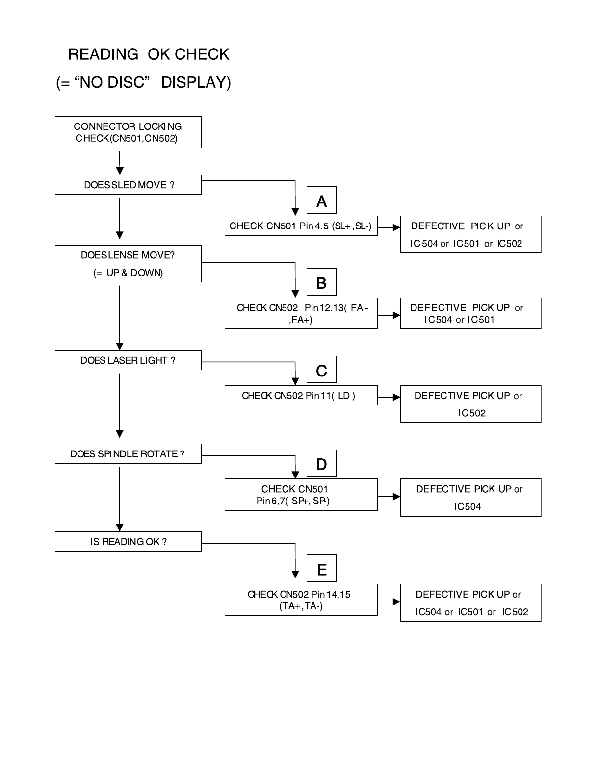
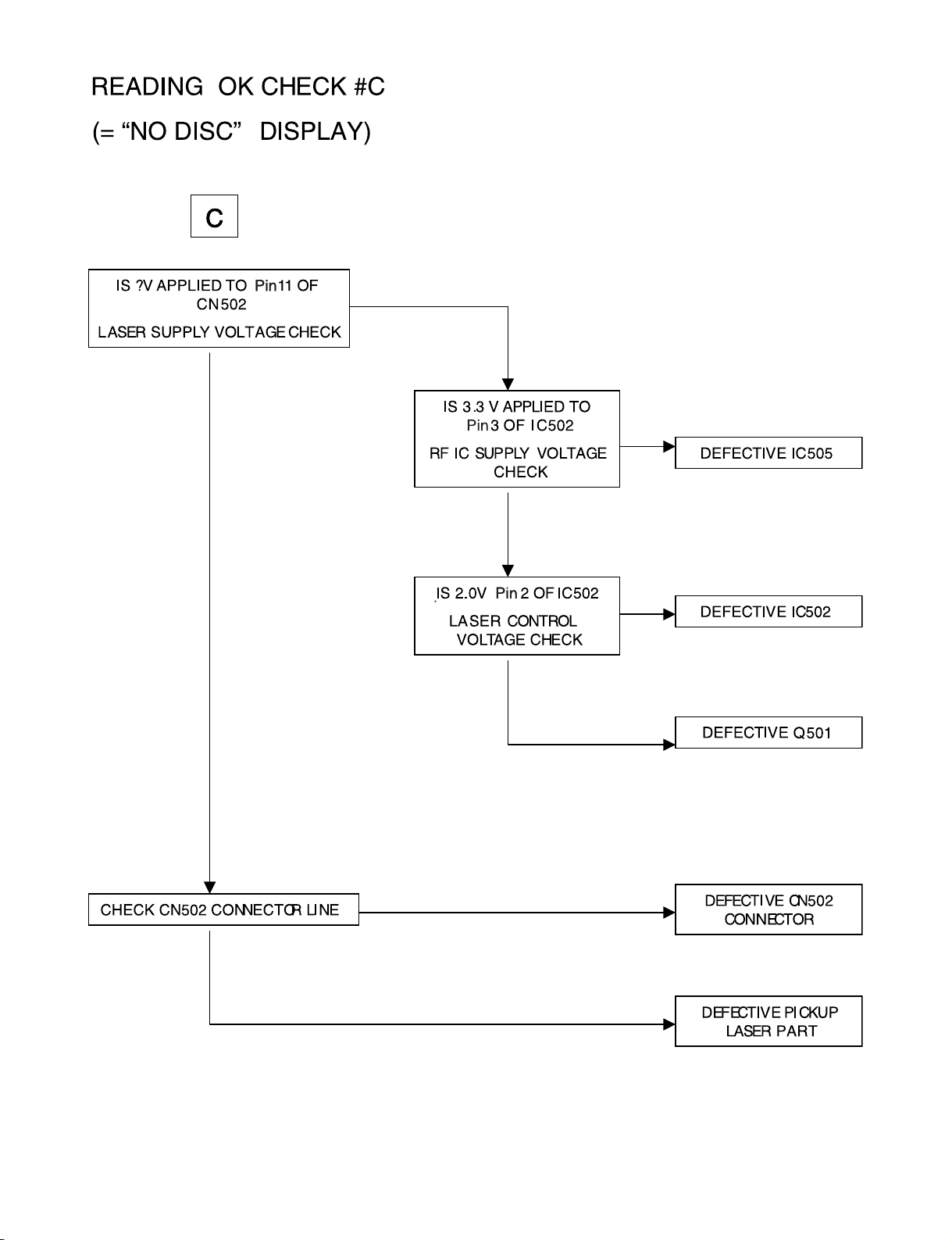
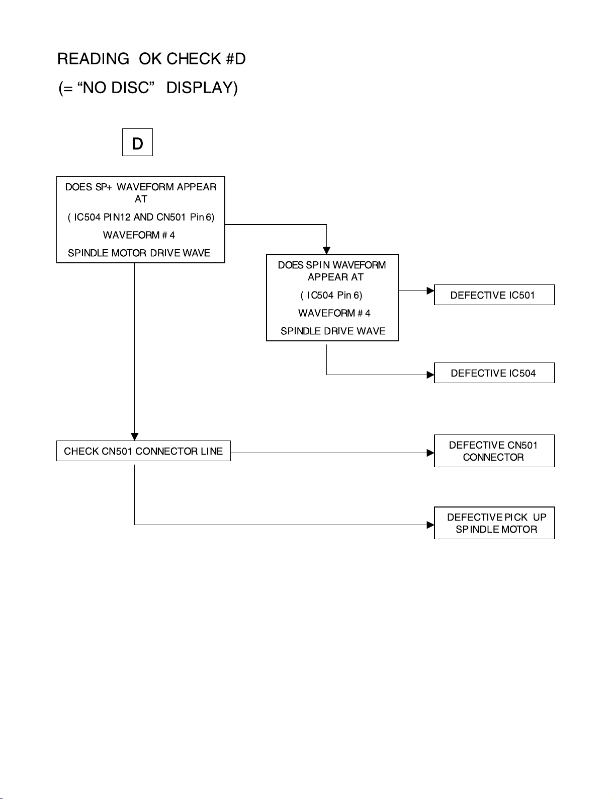
- 2-1 -
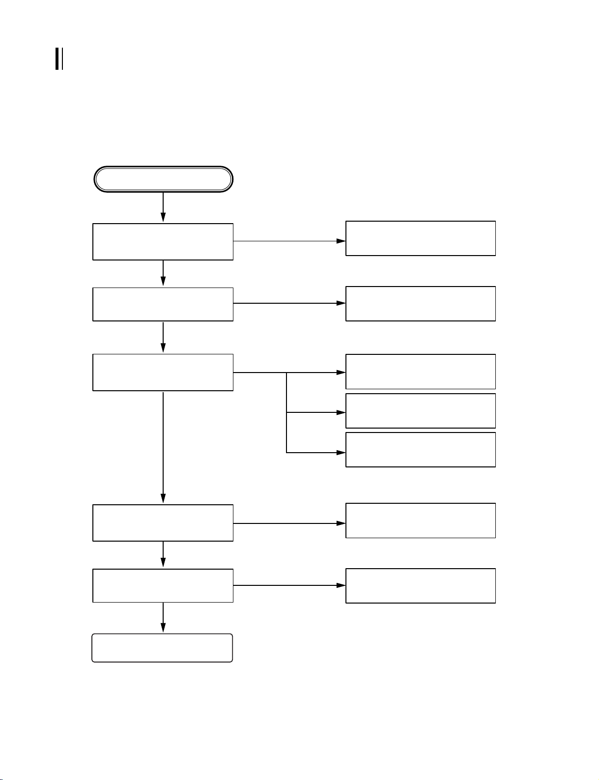
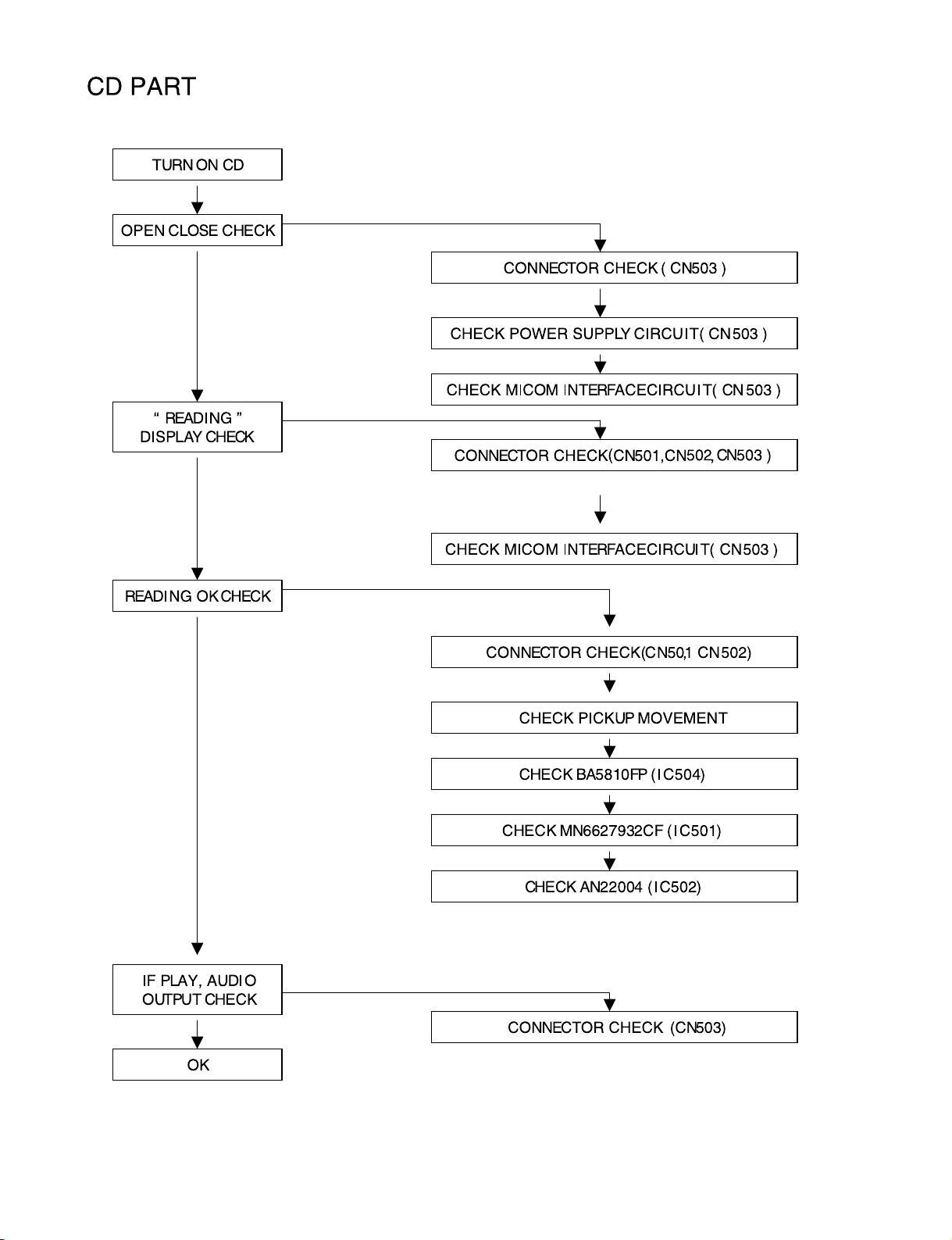
Any Key power on.
Is power turnd on?
DISC loading?
Does initial reading occur?
Can disc be played?
Is audio output supplied?
Check power supply circuitry.
Q260, Q380, Q381, IC401
Pin
83
IC201 Pin2
Check loading supply circuitry.
Q350,Q351,CN505, IC401 Pin84
Check laser circuitry.
Q501, IC502
Check focusing circuitry.
Q501,IC502
Check DISC.
Check tracking servo circuitry.
Q501,IC502
Check audio circuitry.
IC502,IC601,IC801
OK
YES
YES
YES
YES
YES
YES
NO
NO
NO
NO
NO
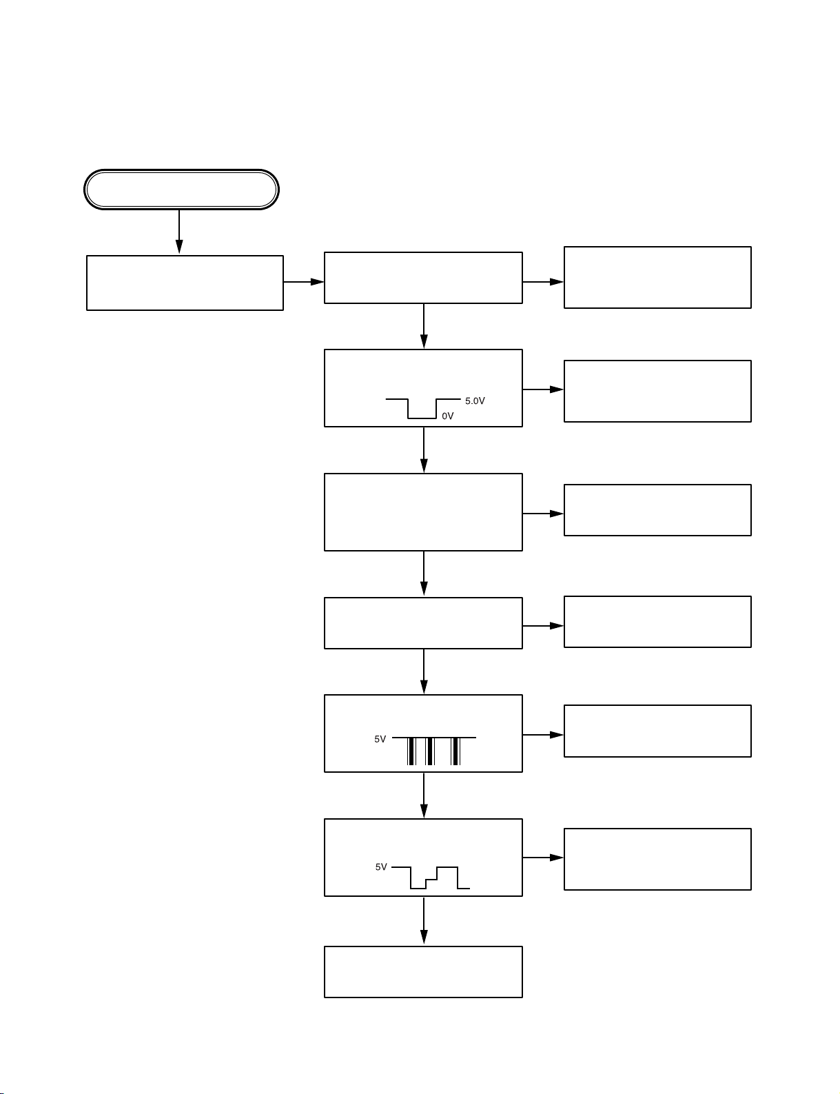
(1) No Power.
SECTION 2. ELECTRICAL
❏ ELECTRICAL TROUBLESHOOTING GUIDE
Page 7
-2-2-
YES
YES
YES
YES
YES
YES
(2) LCD light abnornal.
Any Key power on.
(without DISC)
Do display LCD then light?
Check voltage in the power
supply circuitry.
Power supply circuitry
defective.
Q380,Q381,IC403
Reset circuit defective.
IC821 Surrounding circuit
defective.
X401, C413,C414 defective.
Q260, CN401 front PCB
pattern defective.
IC401, Pin
3, 9, 27, 76
front
PCB pattern defective.
IC901, Surrounding circuit
PCB pattern defective.
Is u-com IC401 reset circuit
normal? Pin11
Is u-com IC401 keyin Pin17, 46
72, 76 5volt input?
Is u-com IC401 Pin 3,9,27,76
output waveform normal?
Is IC901 Com1, Com2, Com3
output waveform normal?
Display LCD connector defective.
Is u-com IC401X1, X2 terminal
Pin15, 16 input?
OSC : 9.8304MHz
NO
NO
NO
NO
NO
NO
NO
Page 8
- 2-3 -
YES
YES
YES
YES
YES
YES
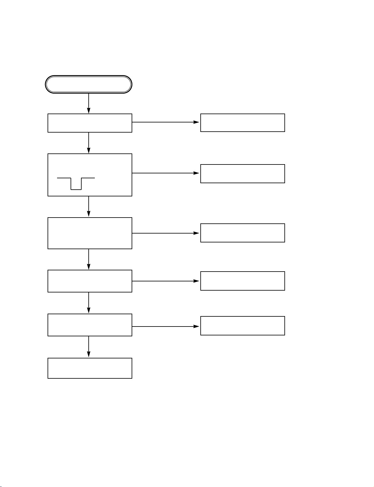
(3) No Hands Free
Hand Free key on.
Is H/F on?
Check whether is power
output (3.3V) to IC502 pin2.
Defect to IC503
Defect to X501, C505, C506.
Defect to MIC901, JK503,
JK504.
Defect to MIC901, JK503,
JK504.
Is it oscillates to IC501
pin 23, 24 by X501 oscillator?
OSC: 19.2MHz
Does signal output appear to
IC501 Pin 26, 27, 33, 34?
Does signal output appear to
IC501 Pin 30, 37.
OK
Does reset circuit appear
normally to IC501 pin56?
3.3V
NO
NO
NO
NO
NO
Page 9
-2-4-
Page 10
- 2-5 -
Page 11
-2-6-
Page 12
- 2-7 -
Page 13

-2-8-
Page 14
- 2-9 -
Page 15
-2-10-
Page 16
- 2-11 -
Page 17

-2-12-
❏ WAVEFORMS OF MAJOR CHECK POINT
#1. MICOM INTERFACE WAVEFORM
(CN503 1 9,2 1 ,1 8,20) during normal play
#2. SLED DRIVE AND MOTOR WAVEFORM
(IC504 pin5, 1 4) when focus search
#3. FOCUS DRIVE AND MOTOR WAVEFORM
(R5 1 3, IC504 pin 1 5)
• When focus search failed or there is no disc on the
tray
• There is disc on tray and focus search success
Page 18

- 2-13 -
#4. SPINDLE DRIVE AND MOTOR WAVEFORM
(IC504 pin6, 1 2) when TOC reading
#5. TRACK DRIVE AND MOTOR WAVEFORM
(R508, IC504 pin23) during normal play
#6. RF, TRACKING AND FOCUS ERROR WAVEFORM
(IC502 pin8, 2 1 , 23) during normal play
Page 19

-2-14-
■ IC401 LC876B
1) PORT ASSIGNMENT
❏
INTERNAL BLOCK DIAGRAM of ICs
2) PORT DESCRIPTION
Pin Name in Micom Name in Model Enable I/O I/O setted Output Format Descripation
1 P16/T1PWML PEV_DO I/O O CMOS To volume controller, data output
2 P17/T1PWMH/BUZ PBEEP I/O O CMOS Beep sound output
3 SI2P0/SO2 PMCM_DO I/O O CMOS To front micom, data output
4 SI2P1/SI2/SB2 PMCM_DI I/O I N-ch From front micom, data input
5 P32/INT4/T1IN PDSP_OGCTL I/O O CMOS RF IC control signal output (gain up)
6 P33/INT4/T1IN PEV_CLK I/O O CMOS Clock for interface with volume controller
7 P34/INT5/T1IN PCD_IFSEQ I/O I N-ch Constant velocity signal input
8 P35/INT5/T1IN PPLL_CE I/O O CMOS PLL IC enable output
9 SI2P2/SCK2/INT5/T1IN/AN12 PMCM_CLK I/O I CMOS Clock output for interface with front micom
10 SI2P3/SCK20/INT5/T1IN/AN13 PSTANDBY I/O O CMOS To power amp, “STANDBY” command output
11 /RESET /RESET I I - Reset
12 XT1/AN10 XT1 I I - Sub clock 32.7 68 KHz
13 XT2/AN11 XT2 I/O O - Sub clock 32.7 68 KHz
14 VSS1 GND - - - Ground
15 CF1 CF1 I I - X’tal 9.8304 MHz
Page 20

- 2-15 -
Pin Name in Micom Name in Model Enable I/O I/O setted Output Format Descripation
16 CF2 CF2 O O - X’tal 9.8304 MHz
17 VDD1 VDD - - - Power supply +5V
18 P80/AN0 PLVL_MTR I/O I N-ch Sound level’s signal input
19 P81/AN1 PS_MTR I/O I N-ch Radio station’s strength signal input
20 P82/AN2 PAF_MUTE I/O O N-ch To tuner pack, AF mute output
21 P83/AN3 PHF_CTR I/O O N-ch Hands free ON/OFF output
22 P84/AN4 PHF_SEND I/O O N-ch Hands free send output
23 P85/AN5 PPWR_MUTE I/O O N-ch To power amp, “MUTE” command output
24 P86/AN6 PCDC_DO I/O O N-ch To CD changer, data output
25 P87/AN7/MICIN PRDS_DI I/O I N-ch From tuner pack, RDS data input
26 P70/INT0/T0LCP/AN8 PRDS_CLK I/O I N-ch From tuner pack, RDS clock input
27 P71/INT1/T0HCP/AN9 PCD_IWRQ I/O I CMOS Sub-Q read standard level signal input
28 P72/INT2/T0IN/NKIN PCDC_DI I/O I CMOS From CD changer, data input
29 P73/INT3/T0IN PMCM_CE I/O I CMOS From front micom, chip select input
30 S0/T0 N.C O O P-ch Not to be used
31 S1/T1 N.C O O P-ch Not to be used
32 S2/T2 N.C O O P-ch Not to be used
33 S3/T3 N.C O O P-ch Not to be used
34 S4/T4 N.C O O P-ch Not to be used
35 S5/T5 N.C O O P-ch Not to be used
36 S6/T6 N.C O O P-ch Not to be used
37 S7/T7 N.C O O P-ch Not to be used
38 S8/T8 N.C O O P-ch Not to be used
39 S9/T9 N.C O O P-ch Not to be used
40 S10/T10 N.C O O P-ch Not to be used
41 S11/T11 N.C O O P-ch Not to be used
42 S12/T12 N.C O O P-ch Not to be used
43 S13/T13 N.C O O P-ch Not to be used
44 S14/T14 N.C O O P-ch Not to be used
45 S15/T15 N.C O O P-ch Not to be used
46 VDD3 VDD - - - Power supply +5
47 S16/PC0 PFRT_DET I/O I P-ch Front detachable switch signal input
48 S17/PC1 PFRT_OPEN I/O I P-ch Front open state input
49 S18/PC2 N.C I/O I P-ch Not to be used
50 S19/PC3 N.C I/O I P-ch Not to be used
51 VP N.C I/O I P-ch Not to be used
52 S20/PC4 N.C I/O I P-ch Not to be used
53 S21/PC5 N.C I/O I P-ch Not to be used
54 S22/PC6 N.C I/O I P-ch Not to be used
55 S23/PC7 N.C I/O I P-ch Not to be used
56 S24/PD0 N.C I/O I P-ch Not to be used
57 S25/PD1 N.C I/O I P-ch Not to be used
58 S26/PD2 N.C I/O I P-ch Not to be used
59 S27/PD3 N.C I/O I P-ch Not to be used
60 S28/PD4 PPER_SNS I/O I P-ch From ISO jack, BACKUP signal input
61 S29/PD5 PACC I/O I P-ch From ISO jack, ACC signal input
62 S30/PD6 PTEL_MUTE I/O I P-ch Telephone mute input
63 S31/PD7 PST I/O I P-ch Stereo indigater’s signal input
64 S32/PE0 PERT_CLOSE I/O I P-ch Front close state input
65 S33/PE1 PCD_SW1 I/O I P-ch In MD, SW1 state input
66 S34/PE2 PCD_SW2 I/O I P-ch In MD, SW2 state input
67 S35/PE3 PCD_SW4 I/O I P-ch In MD, SW4 state input
68 S36/PE4 PLMT_ISW I/O I P-ch In MD, limit switch state input
69 S37/PE5 POPT_IN2 I/O I P-ch For diode option check, signal 1 or 2 inter2
70 S38/PE6 POPT_IN1 I/O I P-ch For diode option check, signal 1 or 2 inter1
71 S39/PE7 POPT_IN0 I/O I P-ch For diode option check, signal 1 or 2 inter0
72 VDD4 VDD - - - Power supply +5
73 S40/PF0 POPT_OUT1 I/O O P-ch For diode option check, signal 2 output
74 S41/PF1 POPT_OUT0 I/O O P-ch For diode option check, signal 1 output
inputportsetted 42
output port setted 54
Used I/O port 67
Interrupt 4
A/D Converter 2
Page 21

-2-16-
■ IC501 MSM7731 (MAIN)
1) PIN CONFIGURATION (TOP VIEW)
Page 22

- 2-17 -
2) BLOCK DIAGRAM
Page 23

-2-18-
■ IC501 MN6627932 (CD)
1) PORT ASSIGNMENT
Page 24

- 2-19 -
2) Block Diagram
SUBCODE
INTERFACE
CIRC
RAM
DRAM
INTERFACE
TXTC K
TXTD
DQSY
SBCK
SUBC TX TD/SMCK
NCLDCK DQSY
FLAG
BLKC K
A9 A0
NRAS
NCAS0
NCAS1
NWE
D3 D0
LRCKIN(EXT1)
BCLKI N(EXT 2)
SRDATAIN(EXT0)
MDAT A
MCL K
ML D
STAT
TI MI NG
GENERATOR
DSL, PLL, VCO
EFM DEMODULATI ON
SYNC INTERPOLAT I ON
CIRC ECC
CDROM ECC
BUS CONTROL
UNIT
(BCU)
SERIAL OUTPUT
INTERFACE (DAO)
OUTPUT PORT
SERVO
CPU
SPINDLE
SERVO
A/ D
CONVERTER
INPUT
PORT
ADPCM
LRCK(TXTCK/EXT1)
BCLK(DQSY/EXT2)
SRDATA(TX TD/EXT0)
IP FLA G FL AG )
SPOUT
TRV P
TRVM
TRP
TRM
FOP
FOM
TBA L
FBAL
LDON
AV
DD
2
AV
SS
2
IREF
ARF
DSLF
RFSW
PLLF
PLLF0
PMCK
SMCK
X2
X1
ADPVC C
FE
TE
RFENV
OFT
NRFDET
BDO
PWMSEL
SPPOL
digital out
DV
DD
DV
SS
TX
MI CRO COMPUTER
INTERACE
MP3
DECORDER
FS
CONVERTOR
DIGITAL FILTER
D/A CONVERTER
ANAL OG
LOW PASS FILTER
OUTL
OUTR
AV
DD
1
AV
SS
1
DRVDD
DSV
Page 25

-2-20-
3) PORT DESCRIPTION
Pin No. Symbol I/O Function
1 D11 I/O DRAM data signal I/O 11
2 D10 I/O DRAM data signal I/O 10
3 D9 I/O DRAM data signal I/O 9
4 D8 I/O DRAM data signal I/O 8
5 UDQM O SDRAM upper byte data mask signal output
6 SDRCK O SDRAM clock signal output
7 A11 O DRAM address signal output 11
8 A9 O DRAM address signal output 9
9 A8 O DRAM address signal output 8
10 A7 O DRAM address signal output 7
11 A6 O DRAM address signal output 6
12 A5 O DRAM address signal output 5
13 A4 O DRAM address signal output 4
14 LDQM O SDRAM lower byte data mask signal output
15 NWE O DRAM write enable signal output
16 NCAS O DRAM CAS control signal output
17 NRAS O DRAM RAS control signal output
18 NCS O SDRAM chip select signal output
19 A3 O DRAM address signal output 3
20 A2 O DRAM address signal output 2
21 A1 O DRAM address signal output 1
22 A0 O DRAM address signal output 0
23 DRVDD1 I Power supply 1 for DRAM interface I/O
24 DVSS1 I Ground 1 for digital circuits
25 A10 O DRAM address signal output 10
26 *BA1 O SDRAM bank selection signal output 1
27 *BA0 O SDRAM bank selection signal output 0
28 DVDD1 I Power supply 1 for internal digital circuits
29 SPOUT O Spindle drive signal output (absolute value)
30 *SPPOL O Spindle drive signal output (polarity)
31 TRVP O Traverse drive signal output (positive polarity)
32 *TRVM O Traverse drive signal output (negative polarity)
33 *TRVP2 O Traverse drive signal output 2 (positive polarity)
34 *TRVM2 O Traverse drive signal output 2 (negative polarity)
35 TRP O Tracking drive signal output (positive polarity)
36 *TRM O Tracking drive signal output (negative polarity)
37 FOP O Focus drive signal output (positive polarity)
38 *FOM O Focus drive signal output (negative polarity)
39 IOVDD1 I Power supply 1 for digital I/O
40 TBAL O Tracking balance adjustment signal output
41 FBAL O Focus balance adjustment signal output
42 FE I Focus error signal input
43 TE I Tracking error signal input
44 ADPVCC I Voltage input for supply voltage monitor
45 RFENV I RF envelope signal input
46 LDON O Laser ON signal output
47 NRFDET I RF detectoion signal input
48 OFT I Off-track signal input
49 BDO I Dropout signal input
50 AVDD1 I Power supply 1 for analog circuits
51 IREF I Analog reference current input
52 ARF I RF signal input
53 DSLF O DSL loop filter pin
54 PWMSEL I PWM output mode selection input Low: Direct High: 3-state
55 PLLF O PLL loop filter pin (for phase comparison)
56 PLLFO O PLL loop filter pin (for speed comparison)
57 AVSS1 I Ground 1 for analog circuits
58 LOOUTL O L-ch audio output for line-out output
59 LOVSS1 I Ground for line-out output
Page 26

- 2-21 -
Pin No. Symbol I/O Function
60 LOOUTR O R-ch audio output for line-out output
61 LOVDD1 I Power supply for line-out output
62 N.C. - 63 TMON1 O Test monitor output 1
64 N.C. - 65 N.C. - 66 TMON2 O Test monitor output 2
67 DVDD3 I Power supply 3 for digital circuits
68 DVSS2 I Ground 2 for digital circuits
69 *EXT0 I/O Expansion I/O port 0
70 *EXT1 I/O Expansion I/O port 1
71 *EXT2 I/O Expansion I/O port 2
72 MCLK I Microcontroller command clock signal input
73 MDATA I Microcontroller command data signal input
74 MLD I Microcontroller command load signal input
75 *STAT O Status signal output
76 *BLKCK O Subcode block clock signal output
77 *SMCK O 4.2336-/8.4672-MHz clock signal output
78 *PMCK O 88.2-kHz clock signal output
79 *TX O Digital audio interface signal output
80 *FLAG O Flag signal output
81 NRST I LSI reset signal input
82 NTEST I Test mode setting input
83 DVSS3 I Ground 3 for digital circuits
84 X1 I Crystal oscillator circuit input
85 X2 O Crystal oscillator circuit output
86 IOVDD2 I Power supply 2 for digital I/O
87 DVDD2 I Power supply 2 for internal digital circuits
88 D2 I/O DRAM data signal I/O 2
89 D1 I/O DRAM data signal I/O 1
90 D0 I/O DRAM data signal I/O 0
91 D3 I/O DRAM data signal I/O 3
92 D4 I/O DRAM data signal I/O 4
93 D5 I/O DRAM data signal I/O 5
94 D6 I/O DRAM data signal I/O 6
95 D7 I/O DRAM data signal I/O 7
96 D15 I/O DRAM data signal I/O 15
97 D14 I/O DRAM data signal I/O 14
98 DRVDD2 I Power supply 2 for DRAM interface I/O
99 D13 I/O DRAM data signal I/O 13
100 D12 I/O DRAM data signal I/O 12
Page 27

-2-22-
■ IC503 M12L16161A
1) PORT ASSIGNMENT
2) Block Diagram
CLK
ADD
LCKE
LRAS
LCBR LWE
CLK
CKE
CS RAS CAS
WE L(U)DQM
LDQM
LWCBR
LCAS
Bank Select
LWE
LDQM
DQI
Data Input Regidter
512K x 16
512K x 16
Column Decoder
Latency & Burst Length
Programming Register
Timing Register
Address Register
Row Decoder
LCBR
LRAS
Sense AMP
I/O Control
Output Buffer
Col. Buffer
Row Buffer
Refresh Counter
Page 28

- 2-23 -
Pin Name Input Function
CLK System Clock Active on the positive going edge to sample all inputs.
CS Chip Select
Disables or enables device operation by masking or enabling all inputs except
CLK, CKE and L(U)DQM.
Masks system clock to freeze operation from the next clock cycle. CKE
CKE Clock Enable should be enabled at least one cycle prior to new command. Disable input
buffers for power down in standby.
A0~A10/AP Address
Row/Column addresses are multiplexed on the same pins. Row address:
RA0~RA10, column address: CA0~CA7
BA Bank Select Address
Selects bank to be activated during row address latch time. Selects bank for
read/write during column address latch time.
RAS Row Address Strobe
Latches row addresses on the positive going edge of the CLK with RAS low.
Enables row access & precharge.
CAS Column Address Strobe
Latches column addresses on the positive going edge of the CLK with CAS
low. Enables column access.
WE Write Enable
Enables write operation and row precharge. Latches data in starting from
CAS, WE active.
L(U)DQM Data Input / Output Mask
Makes data output Hi-Z, tSHZ after the clock and masks the output. Blocks
data input when L(U)DQM active.
DQ0~15 Data Input / Output Data inputs/outputs are multiplexed on the same pins.
VDD/VSS Power Supply/Ground Power and ground for the input buffers and the core logic.
VDDQ/VSSQ Data Output Power/Ground
Isolated power supply and ground for the output buffers to provide improved
noise immunity.
N.C/RFU No Connection/ This is recommended to be left No Connection on the
Reserved for Future Use device.
3) PIN Function table
■ IC504 BA5810FM
28
27
26
25 24
23
22
21 20 19 18 17 16 15
1234 5
6
7 8 9 1011121314
++— + —
+ —
+ —
+ —
7.5k
7.5k
7.5k
7.5k
LOADING PRE
FWE REV
X3
POWER
SAVE
16k
16k
16k
16k
PREVCC
(PRE. LODING)
PREVCC12
(CH1. CH2)
CD1~
CB4
MUTE
POWVCC34
(CH3, CH4)
10k
10k
10k 10k
10k
10k
10k
10k
LEVEL
SHIFT
LEVEL
SHIFT
LEVEL
SHIFT
LEVEL
SHIFT
10k
10k
10k
10k
10k
10k
Page 29

-2-24-
■ IC505 AMC1117
1) Block Diagram
Page 30

- 2-25 -
2) Pin descriptions
■ IC599 BA6289F/BA6417F
1) Block Diagram
Page 31

-2-26-
■ IC601 TDA7437T
1) PINCONNECTION
1
2
3
5
6
4
7
8
9
10
171118 19 20 21 22
44 43 42 41 3940 38 37 36 35 34
28
27
26
24
23
25
33
32
31
29
30
DIFF_R
DIFFGND_R
LOUD_R
IN_R
TREB_R
MUXOUT_R
MONO
STEREO3_R
STEREO2_R
STEREO4_R
STEREO1_R
LOUD_L
DIFFGND_L
DIFF_L
STEREO4_L
STEREO2_L
STEREO1_L
STEREO3_L
CSM
IN_L
MUXOUT_L
MID_RI
TREB-L
AGND
AVDD
DVDD
CREF
ADDR
SCL
SDA
DGND
PAUSE
OUT_LF
SMEXT
BASS_RO
BASS_RI
BASS_LI
MID_RO
BASS_LO
OUT_RF
OUT_LR
MID_LI
OUT_RR
MID_LO
D96AU435B
12 13 14 15 16
Page 32

- 2-27 -
2) BLOCK DIAGRAM
STEREO1_L
SUPPLY
AVDD
AGND
TREBLE BASSMIDDLE
D95AU249B
I
2
C BUS DECODER + LATCHES
SPKR
ATT
SPKR
ATT
TREBLE BASSMIDDLE
SPKR
ATT
SPKR
ATT
SDA
OUT_RR
OUT_RF
OUT_LR
OUT_LF
16
17
18
15
14
13
11
8
9
10
7
6
5
41
42
43 39 3
21 20 12 44 30 31 25 24
2 4 1 23 22 27 26283519
32
29
36
37
38
40
33
34
DIFF_R
VOLUME
+ LOUDN
VOLUME
+ LOUDN
MONO
STEREO2_L
STEREO4_R
ADDR
SCL
DIGGND
S-MUTE
S-MUTE
MUTE
CONTROL
SOFT, ZERO
CSM
PAUSE
SMEXT
BASS_RI
BASS_RO)
MID_RIMID_RO
TREB_R
CREF LOUD_R
INGAIN
MULTIPLEXER
INGAIN
LOUD_L
STEREO3_L
STEREO4_L
DIFF_L
DIFFGND_L
STEREO1_R
STEREO2_R
STEREO3_R
DIFFGND_R
BASS_LIBASS_LOMID_LIMID_LO
TREBL_L
MUXOUT_L
IN_L
MUXOUT_R
IN_R
4 x 470nF
2 x 4.7µF
2 x 4.7µF
5 x 470nF
DVDD
22µF
2.2µF
2.2µF 47nF
47nF 5.6nF
5.6nF 22nF
2.7K
18nF 100nF
5.6K
100nF
22nF
2.7K
18nF 100nF
5.6K
100nF
47nF47nF
Page 33

-2-28-
■ IC602 S4560
1) BLOCK DIAGRAM
■ IC801 TA8275H
1) BLOCK DIAGRAM
Page 34

- 2-29 -
■ IC901 µPD703260GC-105-8EA
Pin Name in Micom Name in Model Enable I/O I/O setted Descripation
1 AVREFO AVREFO - - Analog reference voltage(3.3V)
2 AVSS AVSS - - Analog ground
3 P10/ANO0 PVOLA I/O I Volume encoder A Pin input
4 P11/ANO1 PVOLB I/O I Volume encoder B Pin input
5 AVREF1 AVREF1 - - Analog reference voltage(3.3V)
6 PDH4/A20 PMEMAD19 I/O O External memory address 19 output
7 PDH5/A21 PMEMAD20 I/O O External memory address 20 output
8 IC/FLMD0 N.C - - MASK version : Ground
FLASH version :
Normal mode : pull down
Flash memory programming mode : pull-up
9 VDD VDD - - Power supply(3.3V)
10 REGC N.C - - Regulator control (connect to VSS Via a 4.7µF capacitor)
11 VSS VSS - - Ground
12 X1 X'tal I I X'tal 4.9152 MHz
13 X2 X'tal - - X'tal 4.9152 MHz
14 /RESET /RESET I I Reset(Low active)
15 XT1 N.C I I Connect to Vss
16 XT2 N.C - - Open
17 P02/NMI N.C I/O O Open
18 P03/INTPO/ADTRG N.C I/O O Open
1) PORT DESCRIPTION
Page 35

-2-30-
Pin Name in Micom Name in Model Enable I/O I/O setted Descripation
19 P04/INTP1 PMCM_CE I/O I Chip select input from main micom
20 P05/INTP2//DRST N.C I/O O Open
21 P06/INTP3 PRMC I/O I Remote controller input
22 P40/SIB0/SDA01 PMµDI I/O I Serial data input from main micom
23 P41/SOB0/SCL01 PMµCLK I/O O Serial data output to main micom
24 P42//SCKB0 PMµCLK I/O O Serial clock for interface with main micom
25 P30/TXDA0/SOB4 PLCDDAT0 I/O O LCD data0 output
26 P31/RXDA0/INTP7/SIB4 PLCDDAT1 I/O O LCD data1 output
27
P32/ASCKA0//SCKB4/TIP00/TOP00
PLCDDAT2 I/O O LCD data2 output
28 P33/TIP01/TOP01 PLCDDAT3 I/O O LCD data3 output
29 P34/TIP10/TOP10 PLCDDAT4 I/O O LCD data4 output
30 P35/TIP11/TOP11 PLCDDAT5 I/O O LCD data5 output
31 P36/CTXD0//IETX0 PLCDDAT6 I/O O LCD data6 output
32 P37/CRXD0//IERX0 PLCDDAT7 I/O O LCD data7 output
33 EVSS EVSS - - Power supply for port
34 EVDD EVDD - - Ground for port
35 P38/TXDA2/SDA00 PLCDA0 I/O O LCD address 0 output
36 P39/RXDA2/SCL00 /PLCDWR I/O O LCD data weite signal output
37 P50/TIQ01/KR0/TOQ01/RTP00 N.C I/O I Open
38 P51/TIQ02/KR1/TOQ02/RTP01 N.C I/O I Open
39
P52/TIQ03/KR2/TOQ03/RTP02/DDI
/PLCDCS I/O I LCD driver chip select signal output
40
P53/SIB2/KR3/TIQ00/TOQ00/RTP03/DDO
/PLCDRES I/O O LCD driver reset signal output
41 P54/SOB2/KR4/RTP04/DCK N.C I/O O Open
42 P55/SCKB2/KR5/RTP05/DMS N.C I/O O Open
43 P90/A0/KR6/TXDA1/SDA02 N.C I/O O Open
44 P91/A1/KR7/RXDA1/SCL02 PMEMAD0 I/O O External memory address0 output
45 P92/A2/TIP41/TOP41 PMEMAD1 I/O O External memory address1 output
46 P93/A3/TIP40/TOP40 PMEMAD2 I/O O External memory address2 output
47 P94/A4/TIP31/TOP31 PMEMAD3 I/O O External memory address3 output
48 P95/A5/TIP30/TOP30 PMEMAD4 I/O O External memory address4 output
49 P96/A6/TIP21/TOP21 PMEMAD5 I/O O External memory address5 output
50 P97/A7/SIB1/TIP20/TOP20 PMEMAD6 I/O O External memory address6 output
51 P98/A8/SOB1 PMEMAD7 I/O O External memory address7 output
52 P99/A9//SCKB1 PMEMAD8 I/O O External memory address8 output
53 P910/A10/SIB3 PMEMAD9 I/O O Normal mode : External memory address9 output
Flash memory programming mode : Serial data input
54 P911/A11/SOB3 PMEMAD10 I/O O Normal mode : External memory address10 output
Flash memory programming mode : Serial data input
55 P912/A12//SCKB3 PMEMAD11 I/O O Normal mode : External memory address11 output
Flash memory programming mode : Serial data input
56 P913/A13/INTP4 PMEMAD12 I/O O External memory address12 output
57 P914/A14/INTP5/TIP51/TOP51 PMEMAD13 I/O O External memory address13 output
58 P915/A15/INTP6/TIP50/TOP50 PMEMAD14 I/O O External memory address14 output
59 PDH2/A18 PMEMAD17 I/O O External memory address17 output
60 PDH3/A19 PMEMAD18 I/O O External memory address18 output
61 PCM0//WAIT N.C I/O O Open
62 PCM1/CLKOUT N.C I/O O Open
63 PCM2//HLDAK N.C I/O O Open
64 PCM3//HLDRQ N.C I/O O Open
65 PCT0//WR0 N.C I/O O Open
66 PCT1//WR1 N.C I/O O Open
67 PCT4//RD N.C I/O O Open
68 PCT6/ASTB N.C I/O O Open
69 BVSS BVSS - - Power supply for bus interface
70 BVDD BVDD - - Groind for bus interface
71 PDL0/AD0 PMEMDAT0 I/O I External memory data0 input
72 PDL1/AD1 PMEMDAT1 I/O I External memory data1 input
73 PDL2/AD2 PMEMDAT2 I/O I External memory data2 input
74 PDL3/AD3 PMEMDAT3 I/O I External memory data3 input
input port setted 24
output port setted 36
Used I/O port 60
Interrupt 3
A/D Converter 3
Page 36

- 2-31 -
■ IC902 MR27V3202F
1) PIN CONFIGURATION (TOP VIEW)
2) BLOCK DIAGRAM
Page 37

-2-32-
■ LCD MODULE
1) BLOCK DIAGRAM
3) PIN DESCRIPTIONS
Page 38

- 2-33 -
2) PIN ASSIGNMENT
Page 39

-2-34-
Page 40

❏ MAIN SCHEMATIC DIAGRAM
2-37 2-38
Page 41

2-39 2-40
❏ FRONT SCHEMATIC DIAGRAM
Page 42

2-41 2-42
❏ CDP SCHEMATIC DIAGRAM
Page 43

2-43 2-44
❏ H/F & MOTOR SCHEMATIC DIAGRAM
Page 44

2-35 2-36
❏ BLOCK DIAGRAM
Page 45

2-45 2-46
1. LED P.C.BOARD
2. FRONT P.C. BOARD
(BOTTOM SIDE)
❏ PRINTED CIRCUIT DIAGRAM
Page 46

2. FRONT P.C. BOARD
(TOP SIDE)
2-47 2-48
Page 47

2-49 2-50
3. MAIN P.C. BOARD
(BOTTOM SIDE)
Page 48

2-51 2-52
3. MAIN P.C. BOARD
(TOP SIDE)
Page 49

2-53 2-54
4. CDP P.C. BOARD
Page 50

3-1 3-2
■ CABINET AND MAIN FRAME SECTION
330
268
A43
251
250
257
310
269
263
266
262
252
270
284
289
311
283
280
455
450
288
285
291
290
457
285
453
292
295
294
453
297
299
453
264
261
A41
253
451
451
308
A47
820
A26
286
A40
452
287
307
PN801
A46
A49
300
298
452
452
309
TU101
ANT101
304
282
454
452
306
452
458
*Option
*Option
NOTE) Refer to “SECTION 4 REPLACEMENT
PARTS LIST” in order to look for the
part number of each part.
SECTION 3. EXPLODED VIEWS
Page 51

3-3 3-4
Page 52

-3-5-
825
900
830
827
*Option
❏ Accessory part
 Loading...