

Page 1
SERVICE MANUAL MODEL : LAC-M1500R
DETACHABLE FRONT
PANEL CAR CD RECEIVER
SERVICE MANUAL
MODEL : LAC-M1500R
CAUTION
BEFORE SERVICING THE UNIT, READ THE “SAFETY PRECAUTIONS”
IN THIS MANUAL.
Page 2

- 1-1 -
❍
SECTION 1. SUMMARY
• SERVICING PRECAUTIONS
..........................................................................................................
1-2
• ESD PRECAUTIONS
.......................................................................................................................
1-3
• SPECIFICATIONS
...........................................................................................................................
1-4
❍
SECTION 2. ELECTRICAL
• ELECTRICAL TROUBLESHOOTING GUIDE
.................................................................................
2-1
• WAVEFORMS OF MAJOR CHECK POINT
....................................................................................
2-6
• INTERNAL BLOCK DIAGRAM of ICs
..............................................................................................
2-7
• BLOCK DIAGRAM
.........................................................................................................................
2-17
• SCHEMATIC DIAGRAM
................................................................................................................
2-19
• PRINTED CIRCUIT DIAGRAM
......................................................................................................
2-25
❍
SECTION 3. CABINET MAIN CHASSIS & MECHANISM
• EXPLODED VIEW
...........................................................................................................................
3-1
❍
SECTION 4. REPLACEMENT PARTS LIST
....................................................................
4-1
[CO
Page 3

- 1-2 -
❏ SERVICING PRECAUTIONS
➊ Always disconnect the power source before:
1) Removing or reinstalling any component, circuit board, module or any other instrument assembly.
2) Disconnecting or reconnecting any instrument electrical plug or other electrical connection.
3) Connecting a test substitute in parallel with an electrolytic capacitor in the instrument.
CAUTION: A wrong part substitution or incorrect polarity installation of electrolytic capacitors may result in
an explosion hazard.
➋ Do not defeat any plug/socket B+ voltage interlocks with which instruments covered by this service
manual might be equipped.
❸ Do not apply power to this instrument and or any of its electrical assemblies unless all solid-state
device heat sinks are correctly installed.
❹ Always connect a test instrument’s ground lead to the instrument chassis ground before
connecting the test instrument positive lead. Always remove the test instrument ground lead last.
1) The service precautions are indicated or printed on the cabinet, chassis or components. When servicing,
follow the printed or indicated service precautions and service materials.
2) The Components used in the unit have a specified conflammability and dielectric strength. When
replacing any components, use components which have the same ratings. Components marked in
the circuit diagram are important for safety or for the characteristics of the unit. Always replace with the
exact components.
3) An insulation tube or tape is sometimes used and some components are raised above the printed writing
board for safety. The internal wiring is sometimes clamped to prevent contact with heating components.
Install them as they were.
4) After servicing always check that the removed screws, components and wiring have been installed
correctly and that the portion around the service part has not been damaged. Further check the insulation
between the blades of attachment plug and accessible conductive parts.
SECTION 1. SUMMARY
Page 4
- 1-3 -
❏
ESD PRECAUTIONS
[Electrostatically Sensitive Devices (ESD)]
Some semiconductor (solid state) devices can be damaged easily by static electricity. Such omponents
commonly are called Electrostatically Sensitive Devices (ESD). Examples of typical ESD devices are
integrated circuits and some field-effect transistors and semiconductor chip components. The following
techniques should be used to help reduce the incidence of component damage caused by static electricity.
1) Immediately before handling any semiconductor component or semiconductor-equipped assembly, drain
off any electrostatic charge on your body by touching a known earth ground. Alternatively, obtain and
wear a commercially available discharging wrist strap device, which should be removed for potential
shock reasons prior to applying power to the unit under test.
2) After removing an electrical assembly equipped with ESD devices, place the assembly on a conductive
surface such as aluminum foil, to prevent electrostatic charge buildup or exposure of the assembly.
3) Use only a grounded-tip soldering iron to solder or unsolder ESD devices.
4) Use only an anti-static solder removal device. Some solder removal devices not classified as “anti-static”
can generate electrical charges sufficient to damage ESD devices.
5) Do not use freon-propelled chemicals. These can generate electrical charges sufficient to damage ESD
devices.
6) Do not remove a replacement ESD device from its protective package until immediately before you are
ready to install it. (Most replacement ESD devices are packaged with leads electrically shorted together
by conductive foam, aluminum foil or comparable conductive material).
7) Immediately before removing the protective material from the leads of a replacement ESD device, touch
the protective material to the chassis or circuit assembly into which the device will be installed.
CAUTION: Be sure no power is applied to the chassis or circuit, and observe all other safety precautions.
8) Minimize bodily motions when handling unpackaged replacement ESD devices. (Otherwise harmless
motion such as the brushing together of your clothes fabric or the lifting of your foot from a carpeted floor
can generate static electricity sufficient to damage an ESD device).
[CAUTION. GRAPHIC SYMBOLS]
THE LIGHTNING FLASH WITH APROWHEAD SYMBOL. WITHIN AN EQUILATERAL
TRIANGLE, IS INTENDED TO ALERT THE SERVICE PERSONNEL TO THE PRESENCE
OF UNINSULATED “DANGEROUS VOLTAGE” THAT MAY BE OF SUFFICIENT
MAGNITUDE TO CONSTITUTE A RISK OF ELECTRIC SHOCK.
THE EXCLAMATION POINT WITHIN AN EQUILATERAL TRIANGLE IS INTENDED TO
ALERT THE SERVICE PERSONNEL TO THE PRESENCE OF IMPORTANT SAFETY
INFORMATION IN SERVICE LITERATURE.
Page 5

- 1-4 -
1. GENERAL
Power requirements
.....................................................................................................................
DC12V~15V
Ground system
...................................................................................................................................
Negative
Dimensions(W x H x D)
......................................................................................................
188 x 58 x 166mm
Weight
..............................................................................................................................................
Net: 1.3kg
2. RADIO SECTION
FM AM(MW)
Frequency range 65.0~74.0MHz(Optional), 522~1,620kHz
87.5~108MHz (Optional:530~1,710kHz/ 520~1,620kHz)
Intermediate frequency 10.8MHz 450kHz
Usable sensitivity 10dBµV 28dBµV
Signal to noise ratio 55dB 45dB
3. COMPACT DISC SECTION
Frequency response
.....................................................................................................................
40Hz~20kHz
Channel separation
......................................................................................................................
50dB(1kHz)
Signal to noise ratio ..................................................................................................................................
60dB
4. AUDIO SECTION
Maximum output power
.......................................................................................................................
50W x 4
Speaker impedance
...............................................................................................................
4Ω x 4 or 8Ω x 4
NOTE: The design and specifications are subject to change without notice in the sourse of product
improvement.
❏
SPECIFICATIONS
Page 6
- 2-1 -
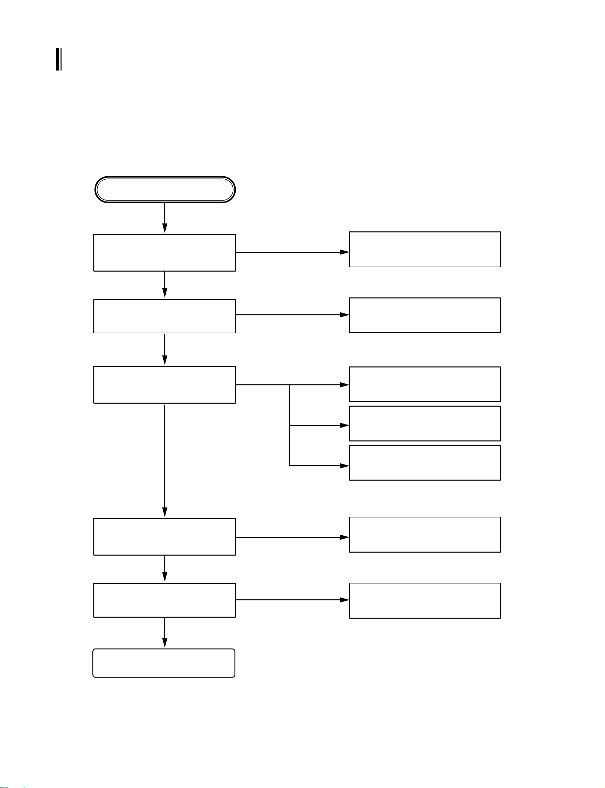
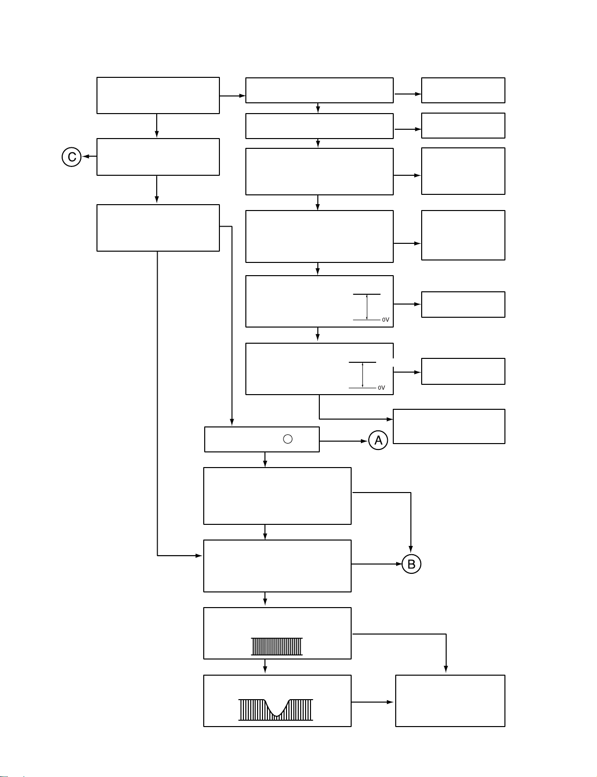
❏ ELECTRICAL TROUBLESHOOTING GUIDE
Any Key power on.
Is power turnd on?
DISC loading?
Does initial reading occur?
Can disc be played?
Is audio output supplied?
Check power supply circuitry.
Q380, Q381, Q382,Q230
IC201 Pin1, IC401 Pin3.
Check loading supply circuitry.
Q350,Q351,Q353,
PN505, IC401 Pin1
Check laser circuitry.
Q501, IC502
Check focusing circuitry.
Q501,IC501.
Check DISC.
Check tracking servo circuitry.
Q501,IC502, IC501.
Check audio circuitry.
IC501,IC601,IC803.
OK
YES
YES
YES
YES
YES
YES
NO
NO
NO
NO
NO
(1) No Power.
SECTION 2. ELECTRICAL
Page 7
- 2-2 -
YES
YES
YES
YES
YES
YES
(2) LCD light abnornal.
Any Key power on.
(without DISC)
Do display LCD then light?
Check voltage in the power supply
circuitry.
Power supply circuitry defective.
Q371,Q372,IC403
• Reset circuit defective.
IC201 Surrounding circuit
defective.
• IC401 pin89 defective.
X401, X422, C412,
C413, C415, C416.
Q260, PN401 front
PCB pattern defective.
IC401, Pin66, 67, 87
front PCB pattern defective.
IC901, Surrounding circuit
PCB pattern defective.
Is u-com IC401 reset circuit
normal? Pin88
Is u-com IC401 keyin Pin9, 37, 51,
52, 64 5volt input?
Is u-com IC401 Pin 66,67,87
output waveform normal?
Is IC901 Com1, Com2, Com3
output waveform normal?
Display LCD connector defective.
Is u-com IC401X1, X2 terminal
Pin38,39,41,42 input?
OSC : 12.5MHz
OSC : 32.768kHz
NO
NO
NO
NO
NO
NO
NO
Page 8
- 2-3 -
(3) Initial reading is not carried out.
NO
NO
NO
NO
NO
NO
NO
NO
NO
NO
NO
NO
YES
YES
YES
YES
YES
YES
YES
YES
YES
YES
YES (with disc)
YES
YES
Slide motor moves
(With disc)
Spindle motor turns
WAVEFORM #1
Does RF waveform appear?
IC502 Pin8
WAVEFORM #2
Check the Data transmission from
CN503(18,20,21) to CD DSP
WAVEFORM #5
Check the Data transmission from
CN503 Pin19 to MICOM
WAVEFORM #5
Check the TRVP
Voltage
IC501 Pin31
Check the change of SL
+, SL - Voltage
IC504 Pin13,14
Check the Voltage change of
CN503 Pin10(6.4~6.8V)
Check the Voltage IC501 Pin31
(1.4V~1.8V)
Defective connector
CN503
Defective IC501
Defective connector
CN503
Defective MICOM
Defective connector
CN503
Defective IC504
Defective IC501
Defective IC504
Defective contact CN502
Defective PICK-UP
Laser light check
A ?
focus coil drive wareform.
TRACKING ERROR wareform
Is rotation normal?
Defective IC501
Defective PICK-UP
Is there no dropout of RF signal?
Does FA+ waveform appear at
IC501 Pin31?
WAVEFORM #3
Does TE waveform appear at
IC502 Pin21?
WAVEFORM #4
1.4~1.8V
3~4V
Page 9
- 2-4 -
NO
NO
NO
NO
NO
NO
When laser does not light.
Is “2.4V~3.4V” applied to pin2 of IC502?
(
➀ 3.4V ➁ 2.4V)
Is power supplied to laser Q501?
(Q 501 collector: about 1.8V)
Is data transferred from
MICOM IC ?
Does voltage appear at
IC504 Pin 13, 14?
Defective MICOM or CN503.
Defective MICOM.
Defective IC502
Defective IC501,IC502
Defective slide motor and/or
connector.(CN501)
Defective LMT SW and/or
connector. (CN501,CN503)
Did pickup return to
innermost circular?
Does it stop at inner pick
circular after shift?
Is defect output from LMT
SW applied to Pin 4 of
PN505?
YES
YES
YES
YES
OPEN
CLOSE
YES
YES
YES
A
OV
Page 10
- 2-5 -
When laser light.
B
When SPINDLE motor dose not turn
C
NO
NO
YES
YES
YES
Laser lights
Check the signal of IC504
Pin 15, 16
WAVEFORM #3
Check the signal FOCUS
SEARCH of IC501 Pin 37
WAVEFORM #3
Defective IC501
Defective IC501
Degraded laser diode
Defective PICK-UP
YES
NO
NO
YES
Check the change for
SPDO Voltage of
IC501 Pin29
WAVEFORM #1
Check the change for SP +, SP
-, Voltage of IC504 Pin11, 12
WAVEFORM #1
Defective IC501
Defective IC504
Defective contact CN502 or
Defective PICK-UP
Page 11

- 2-6 -
❏ WAVEFORMS OF MAJOR CHECK POINT
#1. SPINDLE DRIVE AND MOTOR WAVEFORM
IC501(29), IC544(12) when TOC reading
#2. RF WAVEFORM
IC502(8), IC502(3) during TOC Reading
#3. FOCUS DRIVE AND MOTOR WAVEFORM
IC501(37), IC504(15)
• When focus search failed or there is no disc on tray • There is disc on tray and focus search success
#4. TRACK DRIVE AND MOTOR WAVEFORM
IC504(35), IC504(17) during TOC Reading
#5. MICOM INTERFACE WAVEFORM
CN503(18,19,20,21) during normal play
Page 12

- 2-7 -
■ IC401PD784214A
1) PORT ASSIGNMENT
❏
INTERNAL BLOCK DIAGRAM of ICs
Page 13

- 2-8 -
2) PORT DESCRIPTION
Page 14
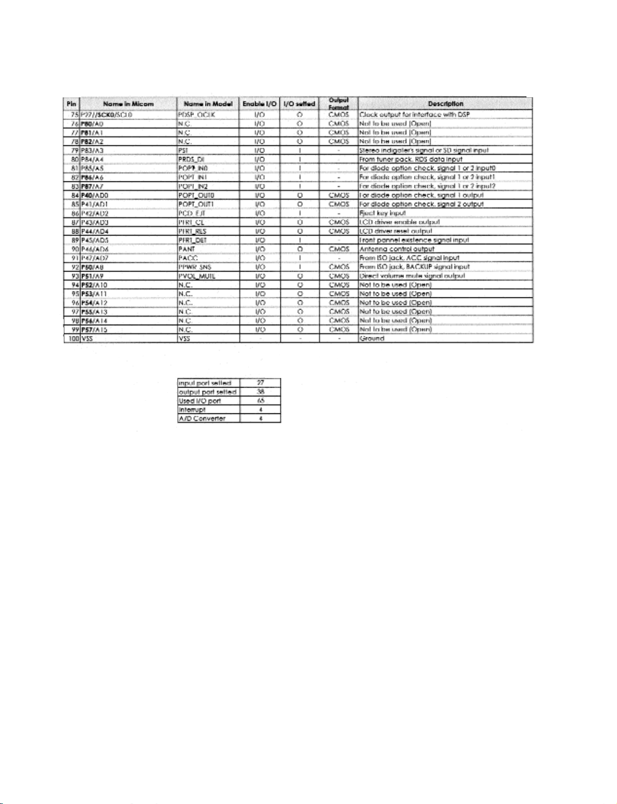
- 2-9 -
Page 15

- 2-10 -
■ IC501 MN6627933CG
Page 16

- 2-11 -
1) Block Diagram
Page 17
- 2-12 -
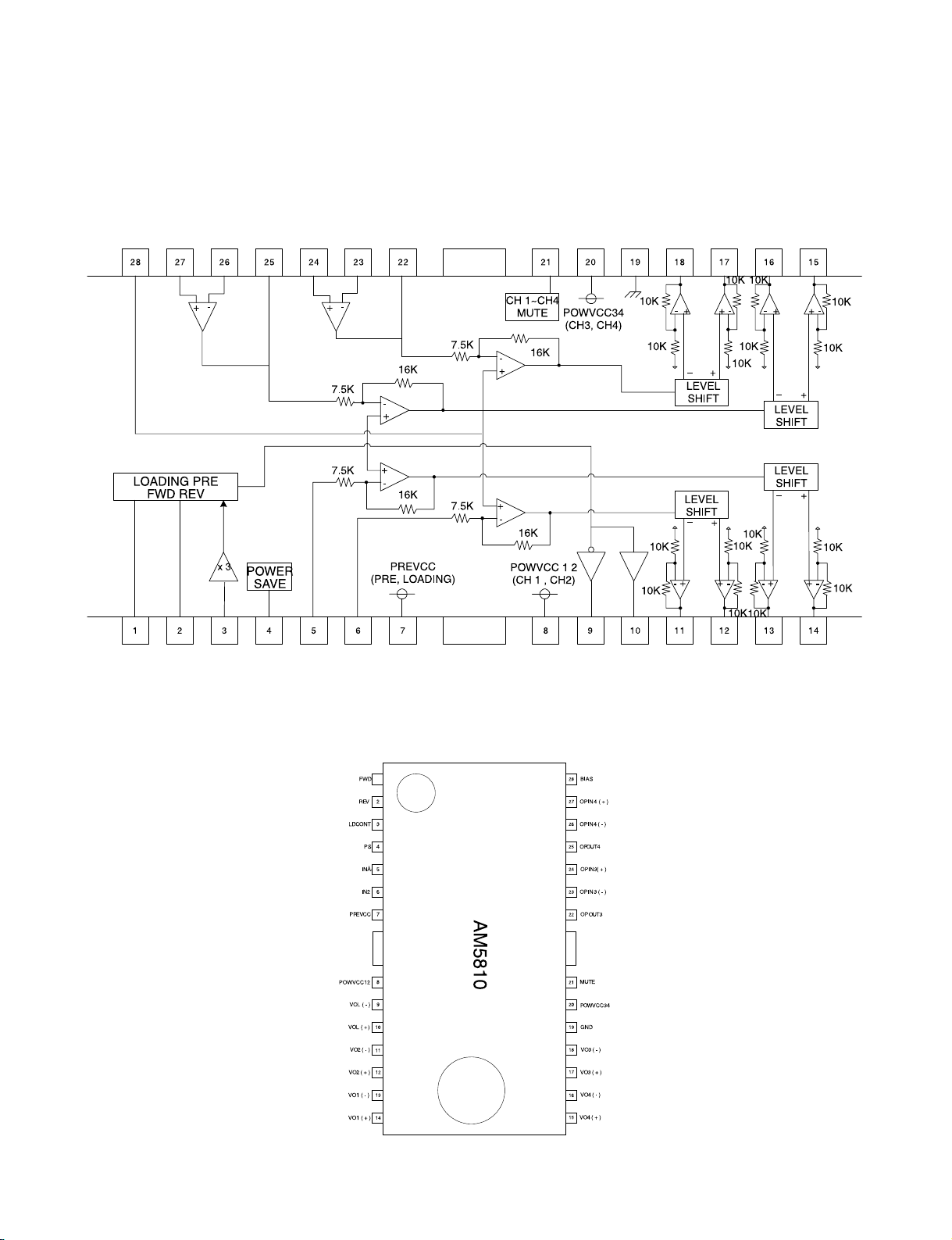
■ IC504 AM5810
1) BLOCK DIAGRAM
2) Pin configuration
Page 18

- 2-13 -
PIN No Pin Name Description
1 FWD Input for loading forward
2 REV Input for loading reverse
3 LDCONT Output control terminal for loading
4 PS Control terminal for power saving mode
5 IN1 Input 1 of CH1
6 IN2 Input 2 of CH2
7 PREVCC Pre and loading unit power supply input terminal
8 POWVCC12 Power unit power supply input terminal (CH1, CH2)
9 VOL ( - ) Inverted output of loading
10 VOL ( + ) Not inverted output of loading
11 VO2 ( - ) Inverted output of CH2
12 VO2 ( + ) Not inverted output of CH2
13 VO1 ( - ) Inverted output of CH1
14 VO1 ( + ) Not inverted output of CH1
15 VO4 ( + ) Not inverted output of CH4
16 VO4 ( - ) Inverted output of CH4
17 VO3 ( + ) Not inverted output of CH3
18 VO3 ( - ) Inverted output of CH3
19 GND Substrate ground
20 POWVCC34 Power unit power supply input terminal (CH3, CH4)
21 MUTE Input for mute control
22 OPOUT3 Output of CH3 OP-ANP
23 OPIN3 ( - ) Inverting input of CH3 OP-ANP
24 OPIN3 ( + ) Not inverting input of CH3 OP-ANP
25 OPOUT4 Output of CH4 OP-ANP
26 OPIN4 ( - ) Inverting input of CH4 OP-ANP
27 OPIN4 ( + ) Not inverting input of CH4 OP-ANP
28 BIAS Input of Bias-Amplifier
3) Pin Descriptions
Page 19

- 2-14 -
■ IC505 AMC1117
1) BLOCK DIAGRAM
Page 20

- 2-15 -
■ IC601TDA7348D
Page 21

- 2-16 -
■ IC801 TA8275H
Page 22

2-17 2-18
❏ BLOCK DIAGRAM
TU101
11,12
CET85XX
20
4,14
16,17,
18,19
2(LR)
9.4V
14V
24
72, 73, 74,
75, 76, 81
58, 60
29, 31, 35, 37
9,10,11,
12,13,14
7,8,20
1,2
4
5,6,23,26 15,16,17,18
10,14
8,12
16
17
27
28
25,26
23,24
10,14
2
11,15
12,14
17,19
7,9
21,23
3,5
6,20
22
Q720,721,722,723
56~60
1~50
61~64
29
14,19
30,31,32,36
68,69,70,71
54
255101124 3 90 6 91 4
43
56,57
66,67
47,48
38
39
7
15, 16, 17, 18
PICK-UP
CD MECHA
(CD303-C004A)
MOTOR
DRIVE IC
(AM5810)
DSP IC
(MN6627933)
RF IC
AN22004A
RADIO VCC
Q310,ZD313
LINE SW/E.VOLUME
9.4V REG
Q360,ZD361
POWER 5V
Q282,Q283
7.5V REG
Q350,351
3.3V REG
IC505
U-COM
uPD784214A
KEY MATRIX
RESISTOR
RADER
RESET
IC201
5V CONVERT
Q260,D233
REG 9V
IC403
Q371
LCD
CONTROL
LCD DRIVER
IC901 PT6524
LCD DISPLAY
DIMMER CONTROL
Q371
PHONE MUTE
Q280,281
ACC DETECTOR
Q230,D231,D232
REMOTE
CONTROL
Q320,321
ANT CONTROL
Q390,391
POWER ON
Q380,381
MUTE
CCNTROL
POWER AMP
IC803
TDA8275HQ
L-SPEAKER
L-SPEAKER
FRONT
R-SPEAKER
REAR
R-SPEAKER
LINE-OUT
(OPTION)
CDC SIGNAL
PN801 #16
BACK_UP
PN801 #10
PWR_ANT
PN801 #6
REMOTE
PN801 #14
ACC
PN801 #5
PHONE
PN801 #11
DIMMER
2(FL,FR)
2(RL,FR)
2(RL,RR)
4-CH
(FL,FR,RL,RR)
IC601 TDA7438D
IC401
Page 23

2-19 2-20
❏ SCHEMATIC DIAGRAM
1. MAIN SCHEMATIC DIAGRAM
Page 24

2-21 2-22
2. FRONT SCHEMATIC DIAGRAM
Page 25

2-23 2-24
3. CDP SCHEMATIC DIAGRAM
Page 26
2-25 2-26
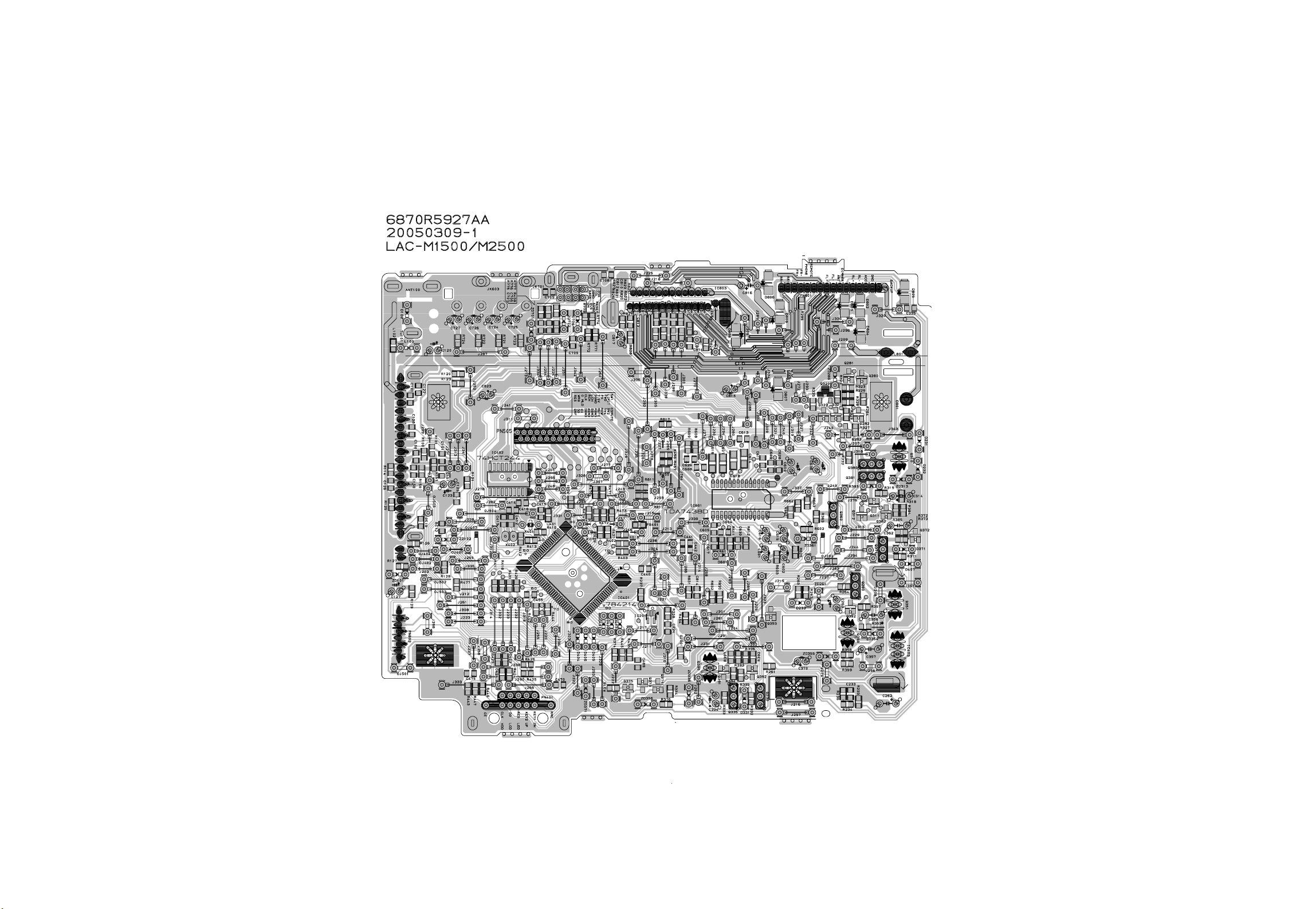
❏ PRINTED CIRCUIT DIAGRAM
1. MAIN P.C. BOARD
Page 27
2-27 2-28
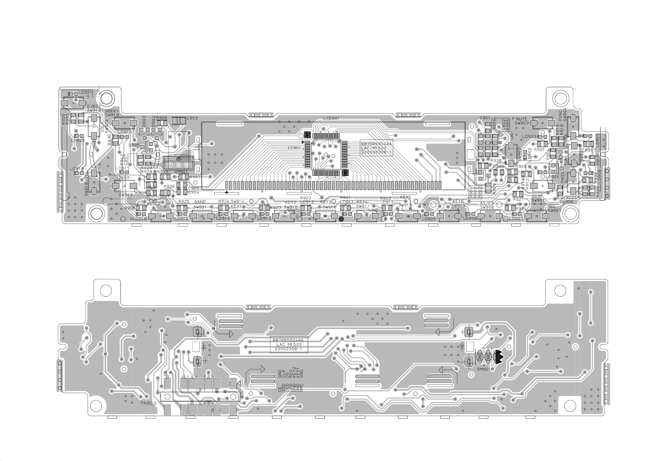
2. FRONT P.C. BOARD
2. FRONT P.C. BOARD
Page 28

2-29 2-30
3. CDP P.C. BOARD 3. CDP P.C. BOARD
Page 29

2-31 2-32
4. LED P.C.BOARD
4. LED P.C.BOARD
Page 30
3-1 3-2
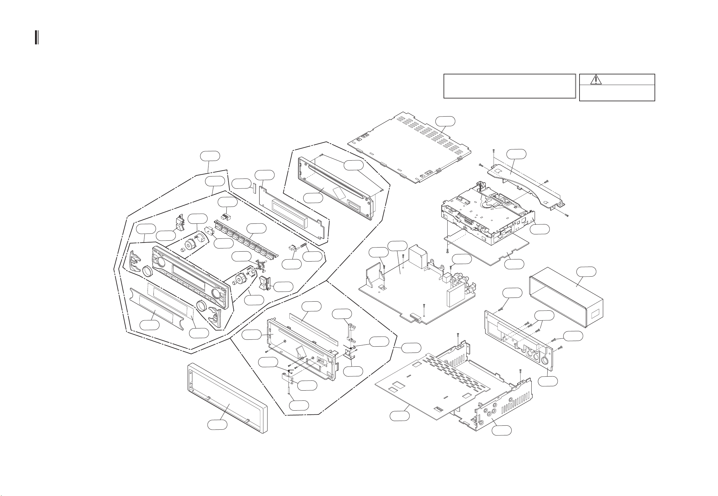
■ EXPLODED VIEW
291
A40
A41
301
450
451
454
290
302
450
450
A46
A26
330
304
270
A42
275
278
277
272
273
274
271
276
259
260
255
254
A43
A45
454
266
264
265
262
263
250
253
252
251
261
A49
CAUTION
Exposed blade will cause
severe injury
NOTE) Refer to “SECTION 4 REPLACEMENT
PARTS LIST” in order to look for the
part number of each part.
SECTION 3. CABINET MAINCHASSIS & MECHANISM
Page 31

 Loading...