

LG L852i Service Manual
Date: May, 2008 / Issue 1.0
Service Manual
Model : L852i
Service Manual
L852i
Internal Use Only

- 3 -
1. INTRODUCTION .............................. 5
1.1 Purpose................................................... 5
1.2 Regulatory Information............................ 5
2. PERFORMANCE...............................7
2.1 System Overview .....................................7
2.2 Usable environment .................................8
2.3 Radio Performance ..................................9
2.4 Current Consumption.............................12
2.5 Antenna BAR .........................................12
2.6. Battery Bar ............................................12
2.7 Sound Pressure Level............................13
2.8 Charging ................................................14
3. TECHNICAL BRIEF ........................15
3.1 Digital Baseband(DBB/MSM6280).........15
3.2. Subsystem(MSM6280) .........................18
3.3 Power Block ...........................................25
3.4 External memory interface .....................30
3.5 H/W Sub System....................................31
4. TROUBLE SHOOTING ...................48
4.1 Power ON Troubleshooting....................48
4.2 Charger Troubleshooting .......................52
4.3 USB Troubleshooting.............................55
4.4 SIM Detect Troubleshooting ..................57
4.5 LCD Troubleshooting .............................63
4.6 Receiver Path ........................................64
4.7 Headset path..........................................66
4.8 Speaker phone path...............................68
4.9 Main microphone ...................................70
4.10 Headset microphone............................72
4.11 Touch Screen Trouble .........................74
4.12 Checking TCXO Block .........................76
4.13 Checking UMTS Block .........................78
5. DOWNLOAD ...................................88
5.1 Introduction ............................................88
5.2 Downloading Procedure.........................88
5.3 Troubleshooting download errors ........102
5.4 Caution.................................................109
6. BLOCK DIAGRAM ........................110
7. Circuit Diagram.............................111
8. BGM Pin Map ................................119
9. PCB LAYOUT................................121
10. Calibration & RF Auto Test
Program (Hot Kimchi)................129
10.1 Configuration of directory...................129
10.2 How to use HOT KIMCHI...................130
11. EXPLODED VIEW &
REPLACEMENT PART LIST ..... 134
11.1 EXPLODED VIEW ............................ 134
11.2 Replacement Parts
<Mechanic component>.................... 137
<Main component> ........................... 141
11.3 Accessory ......................................... 162
Table Of Contents
LGE Internal Use Only
Copyright © 2008 LG Electronics. Inc. All right reserved.
Only for training and service purposes

- 4 -
LGE Internal Use Only
Copyright © 2008 LG Electronics. Inc. All right reserved.
Only for training and service purposes

LGE Internal Use Only
Copyright © 2008 LG Electronics. Inc. All right reserved.
Only for training and service purposes
- 5 -
1.1 Purpose
This manual provides the information necessary to repair, calibration, description and download the
features of this model.
1.2 Regulatory Information
A. Security
Toll fraud, the unauthorized use of telecommunications system by an unauthorized part (for example,
persons other than your company’s employees, agents, subcontractors, or person working on your
company’s behalf) can result in substantial additional charges for your telecommunications services.
System users are responsible for the security of own system.
There are may be risks of toll fraud associated with your telecommunications system. System users
are responsible for programming and configuring the equipment to prevent unauthorized use. The
manufacturer does not warrant that this product is immune from the above case but will prevent
unauthorized use of commoncarrier telecommunication service of facilities accessed through or
connected to it. The manufacturer will not be responsible for any charges that result from such
unauthorized use.
B. Incidence of Harm
If a telephone company determines that the equipment provided to customer is faulty and possibly
causing harm or interruption in service to the telephone network, it should disconnect telephone
service until repair can be done. A telephone company may temporarily disconnect service as long as
repair is not done.
C. Changes in Service
A local telephone company may make changes in its communications facilities or procedure. If these
changes could reasonably be expected to affect the use of the phones or compatibility with the net
work, the telephone company is required to give advanced written notice to the user, allowing the user
to take appropriate steps to maintain telephone service.
D. Maintenance Limitations
Maintenance limitations on the phones must be performed only by the manufacturer or its authorized
agent. The user may not make any changes and/or repairs expect as specifically noted in this manual.
Therefore, note that unauthorized alternations or repair may affect the regulatory status of the system
and may void any remaining warranty.
1. INTRODUCTION
1. INTRODUCTION
LGE Internal Use Only
Copyright © 2008 LG Electronics. Inc. All right reserved.
Only for training and service purposes
E. Notice of Radiated Emissions
This model complies with rules regarding radiation and radio frequency emission as defined by local
regulatory agencies. In accordance with these agencies, you may be required to provide information
such as the following to the end user.
F. Pictures
The pictures in this manual are for illustrative purposes only; your actual hardware may look slightly
different.
G. Interference and Attenuation
A phone may interfere with sensitive laboratory equipment, medical equipment, etc. Interference from
unsuppressed engines or electric motors may cause problems.
H. Electrostatic Sensitive Devices
ATTENTION
Boards, which contain Electrostatic Sensitive Device (ESD), are indicated by the sign.
Following information is ESD handling:
• Service personnel should ground themselves by using a wrist strap when exchange system boards.
• When repairs are made to a system board, they should spread the floor with anti-static mat which is
also grounded.
• Use a suitable, grounded soldering iron.
• Keep sensitive parts in these protective packages until these are used.
• When returning system boards or parts like EEPROM to the factory, use the protective package as
described.
1. INTRODUCTION
- 6 -
LGE Internal Use Only
Copyright © 2008 LG Electronics. Inc. All right reserved.
Only for training and service purposes
2. PERFORMANCE
- 7 -
2.1 System Overview
2. PERFORMANCE
Item Specification
Dimension 101x54x12.7
Weight About 92g
Power 900mA Li-ion
Talk time 140min
Stand-by time Over 350hours(WCDMA DRX2.56s)
Antenna Internal antenna
LCD 3.0” WQVGA(240x400 Dot), 262K TFT Color LCD
Back light Yes
Back light color White
Camera 2Mega pixel(CMOS)
Vibrator Yes
Speaker Yes
C-MIC Yes
Earphone jack Yes(RC-5240)
SIM socket Yes(3.0V & 1.8V)
Volume key Push type(+,-)
Camera key Push type
I/O connect 10pin(RC-5238)
LGE Internal Use Only
Copyright © 2008 LG Electronics. Inc. All right reserved.
Only for training and service purposes
2.2 Usable environment
1) Environment
2) Environment(Accessory)
* CLA : 12~24V(DC).
2. PERFORMANCE
- 8 -
Item Specification
Voltage 3.7V (Typ) ( Shut Down: 3.26)
Operation Temp 20 ~ + 60°C
Storage Temp 30 ~ + 85°C
Humidity 40 ~ 85%
Reference Spec. Min Typ. Max Unit
TA power Available power 100 220 240 Vac
LGE Internal Use Only
Copyright © 2008 LG Electronics. Inc. All right reserved.
Only for training and service purposes
2. PERFORMANCE
- 9 -
2.3 Radio Performance
1) Transmitter -WCDMA Mode
* In case of DCS : [A] -> 1710, [B] -> 1785* In case of PCS : [A] -> 1850, [B] -> 1910
No Item Specification
1 Maximum Output Power
Class3: +24 dBm (+1/-3dB)
Class4: +21dBm(°æ2dB)
2 Frequency Error ±0.1ppm↓
3 Open Loop Power control in uplink ±9dB↓ @normal, ±12dB @extreme
Adjust output(TPC command)
cmd 1dB 2dB 3dB
+1 +0.5/1.5 +1/3 +1.5/4
4 Inner Loop Power control in uplink 0 -0.5/+0.5 -0.5/+0.5 -0.5/+0.5
-1 -0.5/-1.5 -1/-3 -1.5/-4
group(10equal command group)
+1 +8/+12 +16/+24
5 Minimum Output Power -50 dBm↓ (3.84MHz)
Qin/Qout:DPCCH quality levels
6 Out-of-synchronization handling of output power Toff@ DPCCH/Ior:-22->-28dB
Ton@ DPCCH/Ior:-24->-18dB
7 Transmit OFF Power -56 dBm↓ (3.84M)
8 Transmit ON/OFF Time Mask
±25us
PRACH,CPCH, uplink compressed mode
±25us
9 Change of TFC
power varies according to the data rate
DTX: DPCH off
(minise interference between UE)
10 Power setting in uplink compressed ±3dB↓ (after14slots transmission gap)
11 Occupied Bandwidth(OBW) 5 MHz↓ (99% )
LGE Internal Use Only
Copyright © 2008 LG Electronics. Inc. All right reserved.
Only for training and service purposes
* In case of DCS : [A] -> 1710, [B] -> 1785* In case of PCS : [A] -> 1850, [B] -> 1910
2. PERFORMANCE
- 10 -
No Item Specification
-35-15*(∆f-2.5) dBc @∆f=2.5~3.5MHz, 30k
12 Spectrum emission Mask
-35-1*(∆f-3.5) dBc @∆f=3.5~7.5MHz,1M
-39 10*(∆f-7.5) dBc @∆f=7.5~8.5MHz,1M
-49 dBc @∆f=8.5~12.5MHz,1M
13 Adjacent Channel Leakage Ratio(ACLR)
33dB↑ @5MHz, ACP>-50dBm
43dB↑ @10MHz, ACP>-50dBm
-36 dBm @f=9~150KHz, 1k BW
-36 dBm @f=150KHz~30MHz, 10k
-36 dBm @f=30~1000MHz, 100k
-30 dBm @f=1~12.75GHz, 1M
-41 dBm* @1893.5~1919.6MHz, 300k
14
Spurious Emission
-67 dBm* @925~935MHz, 100k
(*: additional requirement)
-79 dBm* @935~960MHz, 100k
-71 dBm* @1805~1880MHz, 100k
-60 dBm* @869~894MHz, 3.84M
-60 dBm* @1930~1990MHz, 3.84M
-60 dBm* @2110~2155MHz, 3.84M
15 Transmit Intermodulation
-31 dBc @5MHz,Interferer -40dBc
-41 dBc @10MHz,Interferer -40dBc
16 Error Vector Magnitude(EVM)
17.5 %↓ (>-20dBm)
(@12.2k, 1DPDCH+1DPCCH)
17 Peak code domain error
-15 dB↓ @SF=4, 768kbps, multi-code
transmission
LGE Internal Use Only
Copyright © 2008 LG Electronics. Inc. All right reserved.
Only for training and service purposes
2. PERFORMANCE
- 11 -
No Item Specification
18 Reference Sensivitivity Level -106.7dBm↓(3.84M)
-25 dBm↑(3.84 MHz)
19 Maximum Input Level -44dBm/3.84MHz(DPCH_Ec)
UE@ +20dBm output power(class3)
20 Adjacent Channel Selectivity(ACS) 33 dB↑
UE@ +20dBm output power(class3)
-56 dBm/3.84MHz @10MHz
21 In-band Blocking
UE@ +20dBm output power(class3)
-44 dBm/3.84MHz @15MHz
UE@ +20dBm output power(class3)
-44 dBm/3.84MHz @f=2050~2095 &
2185~2230 MHz , band a)
UE@ =20dBm output power(class3)
-30 dBm/3.84MHz @f=2025~2050 &
22 Out-band Blocking 2230~2255 MHz, band a)
UE@ +20dBm output power(class3)
-15 dBm/3.84MHz @f=1~2025 &
2255~12500 MHz, band a)
UE@ +20dBm output power(class3)
23 Spurious Response
-44 dBm CW
UE@ +20dBm output power(class3)
-46 dBm CW@10MHz &
24 Intermodulation Characteristic -46dBm/3.84MHz @20MHz
UE@ +20dBm output power(class3)
-57 dBm @f=9KHz~1GHz, 100k BW
-47 dBm @f=1~12.75GHz, 1M
25
-60 dBm @f=1920~1980MHz, 3.84MHz
-60 dBm @f=2110~2170MHz, 3.84MHz
-60 dBm @f=824~849MHz, 3.84MHz
-60 dBm @f=869~894MHz, 3.84MHz
2)Receiver- WCDMA Mode
LGE Internal Use Only
Copyright © 2008 LG Electronics. Inc. All right reserved.
Only for training and service purposes
2. PERFORMANCE
- 12 -
2.4 Current Consumption
(Stand by and Voice Call Test Condition: LCD backlight Off)
(VT Test Condition: Speaker off, LCD backlight On)
2.5 Antenna BAR
2.6. Battery Bar
Static Stand-by Voice Call VT
WCDMA
350 Hours (2.4mA) 140 Mins (350mA) 90 Mins (550mA)
(DRX=2.56) (Tx=10dBm) (Tx=10dBm)
Antenna Bar WCDMA
BAR 3 ->2 -104 ± 2 dBm
BAR 2 ->1 -109 ± 2 dBm
BAR 1 ->0 -112 ± 2 dBm
-114 ± 2 dBm
Indication Voltage
During Idle state During Call state
BAR 3 -> 2
3.720 ± 0.05V 3.660 ± 0.05V
(call maintenance over 40min)
BAR 2 -> 1
3.610 ± 0.05V 3.560 ± 0.05V
(call maintenance over 10min)
BAR 1 -> 0
3.260V ± 0.05V 3.260V ± 0.05V
(Icon Blinking)
Low battery message BAR 1 -> 0
Low battery pop-up BAR 2 -> 1, display one time
Power OFF during call - 80s after Low battery message
Power OFF at stand-by 60s after Low battery message -
LGE Internal Use Only
Copyright © 2008 LG Electronics. Inc. All right reserved.
Only for training and service purposes
2.7 Sound Pressure Level
2. PERFORMANCE
- 13 -
No Test Item Specification
1 Sending Loudness Rating (SLR)
NOM
8±3dB
MAX
2 Sending Frequency Response (SFR) MAX MASK IN
3 Receiving Loudness Rating (RLR)
NOM -2±3dB
MAX -10±3dB
4 Receiving Frequency Response (RFR) MAX MASK IN
5 Side Tone Masking Rating (STMR)
NOM
17dB ↑
MAX
6 Echo Loss (EL)
NOM
46dB ↑
MAX
7 Idle Noise-Sending (INS)
NOM
-64dBm0p
MAX
8 Idle Noise-Receiving (INR)
NOM Under -57dBPA
MAX Under -54dBPA
9 Sending Loudness Rating (SLR)
NOM
8±3dB
MAX
10 Receiving Loudness Rating (RLR)
NOM -1±3dB
MAX -12±3dB
11 Side Tone Masking Rating (STMR)
NOM
25dB ↑
MAX
12 Echo Loss (EL)
NOM
40dB ↑
MAX
13 Idle Noise-Sending (INS)
NOM
Under -55dBm0p
MAX
14 Idle Noise-Receiving (INR)
NOM Under -45dBPA
MAX Under -40dBPA
MS
Headset
A
C
O
U
S
T
I
C
A
I
R

- 14 -
2. PERFORMANCE
2.8 Charging
• Charging Method : CC & CV (Constant Current and Constant Voltage)
• Maximum Charging Voltage : 4.2 V
• Maximum Charging Current : 600mA
• Normal Battery Capacity : 900mA
• Charging Time : Max 3 hours ( except for trickle charging time )
• Full charging indication Current (charging icon stop current) : 140mA
• Low battery message : 3.26 ± 0.05V
• Cut-off : [Idle] 60s after Low battery message
[Call] 80s after Low battery message
LGE Internal Use Only
Copyright © 2008 LG Electronics. Inc. All right reserved.
Only for training and service purposes

LGE Internal Use Only
Copyright © 2008 LG Electronics. Inc. All right reserved.
Only for training and service purposes
3. TECHNICAL BRIEF
- 15 -
3.1 Digital Baseband(DBB/MSM6280)
3.1.1 General Description
A. Features(MSM6280)
■ Support for multimode operation - HSDPA, tri-band WCDMA (UMTS), quad GSM/GPRS
■ Support for HSDPA downlink up to 3.6Mbps (initial commercial release will support 3.6Mbps
■ HSDPA. Later releases will have support for 7.2 Mbps HSDPA)
■ Support for WCDMA (UMTS) uplink data rate up to 384 kbps
■ High-performance ARM926EJ-S running at up to 225 MHz (later at 270 MHz for 7.2 Mbps
HSDPA)
■ ARM Jazelle Java hardware acceleration for faster Java-based games and other applets
■ QDSP4000 high-performance DSP cores
■ Integrated gpsOne position location technology functionality
■ Integrated Bluetooth 1.2 baseband processor for wireless connectivity to peripherals
■ Qcamera™ with 15 fps QVGA viewfinder resolution, and support for 4 MP camera sensors
■ Direct interface to digital camera module with video front end (VFE) image processing
■ True 3D graphics for advanced wireless gaming
■ SecureMSM v2.0 includes support for Open Mobile Alliance (OMA) DRM v2.0, SIM-lock and IMEI
integrity. Support for Q-fuse.
■ Audio on par with portable music players
■ Vocoder support (AMR, FR, EFR, HR)
■ Advanced 14 x 14 mm, 0.5 mm pitch, 409-pin lead-free CSP packaging technology
■ SD/SDIO hardware support
LGE Internal Use Only
Copyright © 2008 LG Electronics. Inc. All right reserved.
Only for training and service purposes
3. TECHNICAL BRIEF
- 16 -
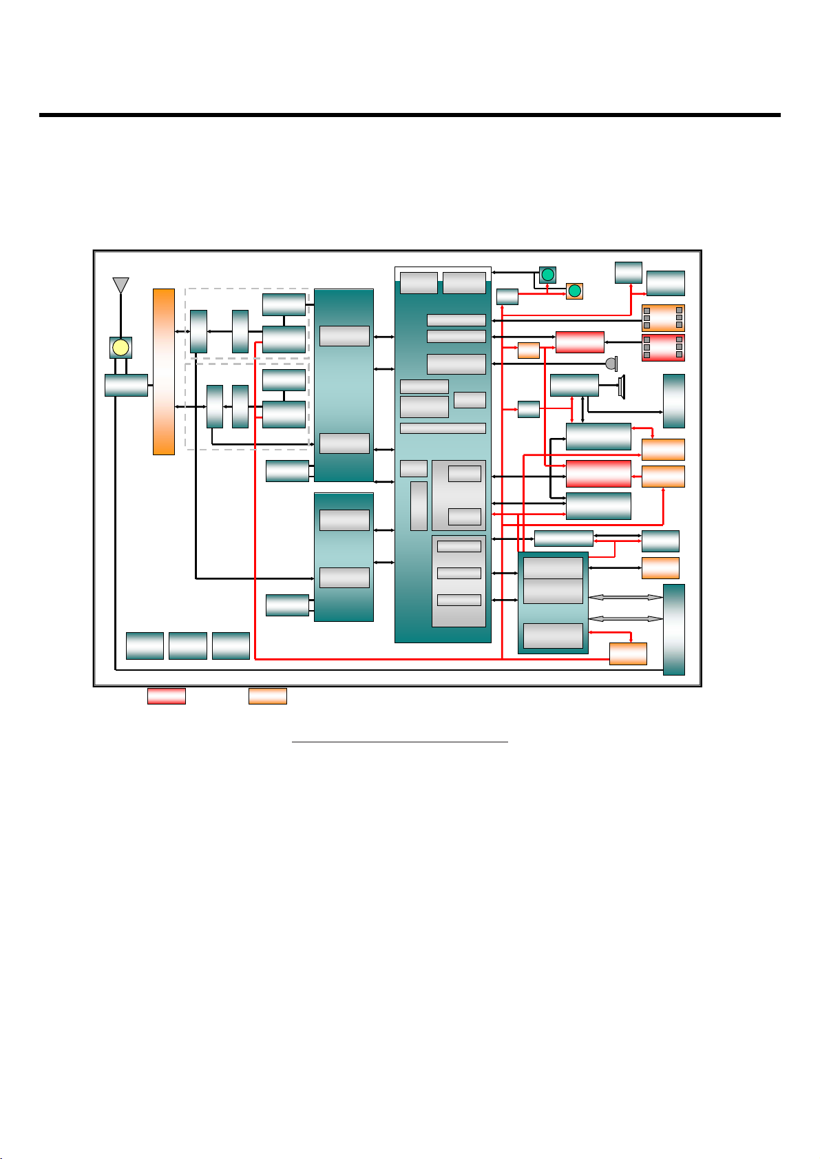
Prada Block Diagram
PM6650
MSM6280
Connectivity
CAM I/F
H.264
MPEG
KEYPAD I/F
I2C I/F
AUDIO
PLL
QDSP 4000
ARM926ejs
With Jazelle
Modem QDSP 4000
Dual Memory
Bus
EBI2
EBI1
IRDA/UART
USIM
USB
SSBI
GRAPICS
LDO
Camera 2M A/F
Camera VGA
CAM
LED
LED
Driver
TX_SAW
RTR6275
RFR6275
W-VCO1
LNA1
W-VCO2
LNA2
TX_SAW
WCDMA
PAM
WCDMA
PAM
Coupler Coupler
Duplexer
Duplexer
RX_SAW
Diplexer
SPDT
RX_SAW
TCXO
19.2MHz
XTAL
48MHz
XTAL
32.768KHz
Key
pad
Touch
Screen
Audio
Processor
LCD
(3.0î WQVGA)
NAND 2Gbits
SDRAM 1Gbits
RUIM Level
Translator
USB
Tranciever
Charge &
Battery Control
RC Formattor
IrDA(RC)
USIM
Micro SD
LCD
B/L Driver
DAC/AMP
ARIB A ConnectorEar Jack
Sensor IC
LDO
LDO
Battery
MIC
Speaker
&
Receiver
USB
+5V
SSBI
SSBI
TX
IQ
RX
IQ
TX
IQ
RX
IQ
RF
Connector
WCDMA
800MHz
WCDMA
2100MHz
New parts
Changed parts
Figure. Simplified Block Diagram
LGE Internal Use Only
Copyright © 2008 LG Electronics. Inc. All right reserved.
Only for training and service purposes
3. TECHNICAL BRIEF
- 17 -
3.1.2 Block Diagram(MSM6280)
Figure. Simplified Block Diagram of MSM6280
Camera 2M
Camera 0.3M
CAMERA
PROCESSING
(Default 8bit
Interface)
GRAPHICS
Open GL ES
3D, 2D
VIDEO
MPEG-4
AUDIO
AAC,
EVRC, QCELP
AMR, CMX
SDRAM
1G
EBI 1 EBI 2
DUAL MEMORY BUS
MSM6280
Modem QDSP 4000
PLL
QDSP 4000
CONNECTIVITY
F/
I
d
ap
y
eK
GATJ
NAND Flash
2G
ARM 926ejs
With Jazelle
1TRAU
BSU
LCD
(3.0î )
GSM/GPRS
processor
UMTS, WCDMA,
HSDPA processor
IBSS
1
M
I
UR
C
IM
/ 2
P
T
R
AU
RF SSBI
Rx ADC
Tx DAC
GPIO
ediS
yeK
nnoC O/I
PM6650
BSU
USIM

LGE Internal Use Only
Copyright © 2008 LG Electronics. Inc. All right reserved.
Only for training and service purposes
3. TECHNICAL BRIEF
- 18 -
3.2. Subsystem(MSM6280)
3.2.1 ARM Microprocessor Subsystem
The MSM6280 device uses an embedded ARM926EJ-S microprocessor. This microprocessor,
through the system software, controls most of the functionality for the MSM, including control of the
external peripherals such as the keypad, LCD, SDRAM, and NAND-Flash devices. Through a
QUALCOMM proprietary serial bus interface (SBI) the ARM926EJ-S configures and controls the
functionality of the RTR6275, RFR6275 and PM6650 devices.
3.2.2 WCDMA R99 features
The MSM6280 device supports release 99 June 2004 of the W-CDMA FDD standard, including the
following features:
■ All modes and data rates for W-CDMA frequency division duplex (FDD), with the following
restrictions:
❏ The downlink supports the following specifications:
- Up to four physical channels, including the broadcast channel (BCH), if present
- Up to three dedicated physical channels (DPCHs)
- Spreading factor (SF) range support from 4 to 256
- The following transmit diversity modes are supported:
Space time transmit diversity (STTD)
Time-switched transmit diversity (TSTD)
Closed-loop feedback transmit diversity (CLTD)
■ The uplink supports the following specifications:
❏ The uplink provides the following UE support:
- One physical channel, eight TrCH, and 16 TrBks starting at any frame boundary
- A maximum data rate of 384 kbps
❏ Full SF range support from 4 to 256
■ SMS (CS and PS)
■ PS data rate - 384 kbps DL / 384 kbps UL
■ CS data rate - 64 kbps DL / 64 kbps UL
■ AMR (all rates)
3.2.3 GSM features
The following GSM modes and data rates are supported by the MSM6280 device hardware. Support
modes conform to release '99 specifications of the sub-feature.
■ Voice features
❏ FR
❏ EFR

LGE Internal Use Only
Copyright © 2008 LG Electronics. Inc. All right reserved.
Only for training and service purposes
3. TECHNICAL BRIEF
- 19 -
❏ AMR
❏ HR
❏ A5/1, A5/2, and A5/3 ciphering
■ Circuit-switched data features
❏ 9.6k
❏ 14.4k
❏ Fax
❏ Transparent and non-transparent modes for CS data and fax
❏ No sub-rates are supported.
3.2.4 GPRS features
■ Packet switched data (GPRS)
❏ DTM (Simple Class A) operation
❏ Multi-slot class 12 data services
❏ CS schemes: CS1, CS2, CS3, and CS4
❏ GEA1, GEA2, and GEA3 ciphering
■ Maximum of four Rx timeslots per frame
3.2.5 MSM6280 device audio processing features
■ Integrated wideband stereo CODEC
❏ 16-bit DAC with typical 88 dB dynamic range
❏ Supports sampling rates up to 48 kHz on the speaker path and 16 kHz on the microphone path
■ VR- Voice mail + voice memo
■ Acoustic echo cancellation
■ Audio AGC
■ Audio Codecs: AMR-NB, AAC, AAC Plus, Enhanced AAC Plus, Windows Audio v9, Real Audio 8
(G2)
■ Internal vocoder supporting AMR, FR, EFR, and HR
3.2.6 MSM6280 microprocessor subsystem
■ Industry standard ARM926EJ-S embedded microprocessor subsystem
❏ 16 kB instruction and 16 kB data cache
❏ Instruction set compatible with ARM7TDMI®
❏ ARM version 5TEJ instructions
❏ Higher performance 5 stage pipeline, Harvard cached architecture
❏ Higher internal CPU clock rate with on-chip cache

■ Java hardware acceleration
■ Enhanced memory support
Please note that NOR/PSRAM will not be supported on MSM6280.
❏ 75 MHz and 90 MHz bus clock for SDRAM
❏ 32-bit SDRAM
❏ Dual memory buses separating the high-speed memory subsystem (EBI1) from low-speed
peripherals (EBI2) such as LCD panels
❏ 1.8 V or 2.6 V memory interface support (excluding EBI1)
❏ NAND FLASH memory interface
- 8/16-bit data I/O width NAND flash support
- 1- or 4-bit ECC
- 512-byte/2KB page-size support
- 2 chip selects supported for NAND Flash
❏ Boot from NAND
❏ Low-power SDRAM (LP-SDRAM) interface
■ Internal watchdog and sleep timers
3.2.7 Supported interface features
■ USB On-the-Go core supports both slave and host functionality
■ Three universal asynchronous receiver transmitter (UART) serial ports
■ USIM controller (via UART)
■ Integrated 4-bit secure digital (SD) controller for SD and Mini SD cards
■ Parallel LCD interface
■ General-purpose I/O pins
■ External keypad interface
3.2.8 Supported multimedia features
■ Provide additional general purpose MIPS by using:
❏ Two QDSP4000s
❏ Dedicated hardware accelerators and compression engines
■ Improve Java, BREW, and game performance
❏ Integrated Java and 2D/3D graphics accelerator with Sprite engine
■ Enable various accessories via USB host connectivity.
❏ Integrated USB host controller functionality
■ Enable compelling visual and audio applications.
LGE Internal Use Only
Copyright © 2008 LG Electronics. Inc. All right reserved.
Only for training and service purposes
3. TECHNICAL BRIEF
- 20 -

LGE Internal Use Only
Copyright © 2008 LG Electronics. Inc. All right reserved.
Only for training and service purposes
3. TECHNICAL BRIEF
- 21 -
Qcamera
■ High-quality digital camera processing, supporting CCD or CMOS image sensors up to 4-megapixel
with 15 fps capture rate
■ 15 fps QVGA viewfinder
Qtv
■ Audio and video decoder that supports VOD, MOD and Broadcast multimedia services.
■ Audio Codecs supported: AMR-NB, AAC, AAC Plus, Enhanced AAC Plus, Windows® Audio v9,
RealAudio® v8
■ Integrated stereo wideband Codec for music/digital clips
■ CMX
■ Video Codecs supported: MPEG-4, H.263, H.264, Windows Media® v9 and RealNetworks® v10
Video telephony services: Qvideophone
■ A two-way mobile video conferencing solution that delivers 15 fps @ QCIF
■ Video Codecs supported: MPEG-4 and H.263
■ Audio Codecs supported: AMR-NB.
Qcamcorder
■ Real time mobile video encoder
■ Video Codecs supported: MPEG-4, H.263.H.264
■ Audio Codecs supported: AMR-NB, AAC
■ Recording performance: 15 fps @ QVGA, 384 kbps
CMX (MIDI and still image, animation, text, LED/vibrate support)
■ 72 simultaneous polyphonic tones
■ 44 kHz sampling rate
■ 512 kB wave table
■ Support of universal file formats
❏ Standard MIDI Format (SMF)
❏ SP-MIDI
❏ SMAF Audio playback (MA-2, MA-3, MA-5)
❏ XMF/OLS
❏ MFil (requires Docomo license)
■ PNG decoder
■ Pitch bend range support
■ LED/vibrate support
■ Scalable Vector Graphics (SVG- Tiny 1.1 + SVG Tiny 1.2)
■ MLZ decoder
■ Integrated PNG/SAF A.T.
LGE Internal Use Only
Copyright © 2008 LG Electronics. Inc. All right reserved.
Only for training and service purposes
3. TECHNICAL BRIEF
- 22 -
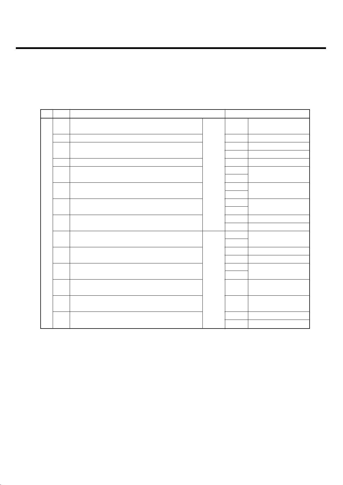
Table. 3.2 Summary of MSM6280 device features

LGE Internal Use Only
Copyright © 2008 LG Electronics. Inc. All right reserved.
Only for training and service purposes
3. TECHNICAL BRIEF
- 23 -
3.2.9 Serial Bus Interface(SBI)
The MSM6280 device’s SSBI is designed specifically to be a quick, low pin count control protocol for
QUALCOMM’s RTR6275, RFR6275 and PM6650 ASICs. Using the SSBI, the RTR6275, RFR6275,
and PM6650 devices can be configured for different operating modes and for minimum power
consumption, extending battery life in Standby mode. The SSBI also controls DC baseband offset
errors.
3.2.10 Wideband CODEC
The MSM6280 device integrates a wideband voice/audio CODEC into the mobile station modem
(MSM). The CODEC supports two differential microphone inputs, one differential earphone output, one
single-ended earphone output, and a differential analog auxiliary interface.
The CODEC integrates the microphone and earphone amplifiers into the MSM6280 device, reducing
the external component count to just a few passive components. The microphone (Tx) audio path
consists of a two-stage amplifier with the gain of the second stage set interally. The Rx/Tx paths are
designed to meet the ITU-G.712 requirements for digital transmission systems.
3.2.11 Vocoder Subsystem
The MSM6280 device’s QDSP4000 supports AMR,FR,EFR and HR. In addition, the QDSP4000 has
modules to support the following audio functions: DTMF tone generation, DTMF tone detection, Tx/Rx
volume controls, Tx/Rx automatic gain control (AGC), Rx Automatic Volume Control (AVC), EarSeal
Echo Canceller (ESEC), Acoustic Echo Canceller (AEC), Noise Suppression (NS), and programmable,
13-tap, Type-I, FIR, Tx/Rx compensation filters. The MSM6280 device’s integrated ARM9TDMI
processor downloads the firmware into the QDSP4000 and configures QDSP4000 to support the
desired functionality.
3.2.12 ARM Microprocessor subsystem
The MSM6280 device uses an embedded ARM926EJ-S microprocessor. This microprocessor,
through the system software, controls most of the functionality for the MSM device, including control of
the external peripherals such as the keypad, LCD, RAM, ROM, and EEPROM devices. Through a
generic single serial bus interface (SSBI) the ARM926EJ-S configures and controls the functionality of
the RFR6275, RTR6275, and PM6650 devices.

LGE Internal Use Only
Copyright © 2008 LG Electronics. Inc. All right reserved.
Only for training and service purposes
3. TECHNICAL BRIEF
- 24 -
3.2.13 Mode Select and JTAG Interfaces
The mode pins to the MSM6280 device determine the overall operating mode of the ASIC. The options
under the control of the mode inputs are Native mode, which is the normal subscriber unit operation,
ETM mode, which enables the built-in trace mode, and test mode for factory testing. The MSM6280
device meets the intent of the ANSI/IEEE 1149.1A-1993 feature list. The JTAG interface can be used
to test digital interconnects between devices within the mobile station during manufacture.
3.2.14 General-Purpose Input/Output Interface
The MSM6280 device has general-purpose bidirectional input/output pins. Some of the GPIO pins
have alternate functions supported on them. The alternate functions include USB interface, additional
RAM, ROM, general-purpose chip selects, parallel LCD interface, and a UART interface. The function
of these pins is documented in the various software releases.
3.2.15 UART
The MSM6280 device employs three UARTs. UART1 has dedicated pins while UART2 and UART3
share multiplexed pins.
■ UART1 for data
■ UART2 (can be used for USIM interface)
■ UART3 for data
3.2.16 USB
The MSM6280 device integrates a universal serial bus (USB) controller that supports both
unidirectional and bidirectional transceiver interfaces. The USB controller acts as a USB peripheral
communicating with the USB host.

LGE Internal Use Only
Copyright © 2008 LG Electronics. Inc. All right reserved.
Only for training and service purposes
3. TECHNICAL BRIEF
- 25 -
3.3 Power Block
3.3.1 General
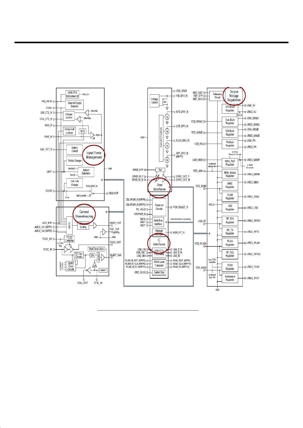
MSM6280, included RF, is fully covered by PM6650(Qualcomm PMIC). PM6650 cover the power of
MSM6280, MSM memory, RF block, Bluetooth, Micro SD, USIM and TCXO.
Major power components are :
PM6650-3P (U400, Main PCB) : Phone power supply
MAX8645Y (U601, Slide PCB) : LCD Backlight charge pump
3.3.2 PM6650
The PM6650 device (Figure 1-1) integrates all wireless handset power management. The power
management portion accepts power from all the most common sources - battery, external charger,
adapter, coin cell back-up - and generates all the regulated voltages needed to power the appropriate
handset electronics. It monitors and controls the power sources, detecting which sources are applied,
verifying that they are within acceptable operational limits, and coordinates battery and coin cell
recharging while maintaining the handset electronics supply voltages. Eight programmable output
voltages are generated using low dropout voltage regulators, all derived from a common trimmed
voltage reference.
A dedicated controller manages the TCXO warm-up and signal buffering, and key parameters (undervoltage lockout and crystal oscillator signal presence) are monitored to protect against detrimental
conditions.
MSM device controls and statuses the PM6650 IC using Single Serial Bus Interface (SSBI)
supplemented by an Interrupt Manager for time-critical information. Another dedicated IC Interface
circuit monitors multiple trigger events and controls the power-on sequence.
LGE Internal Use Only
Copyright © 2008 LG Electronics. Inc. All right reserved.
Only for training and service purposes
3. TECHNICAL BRIEF
- 26 -
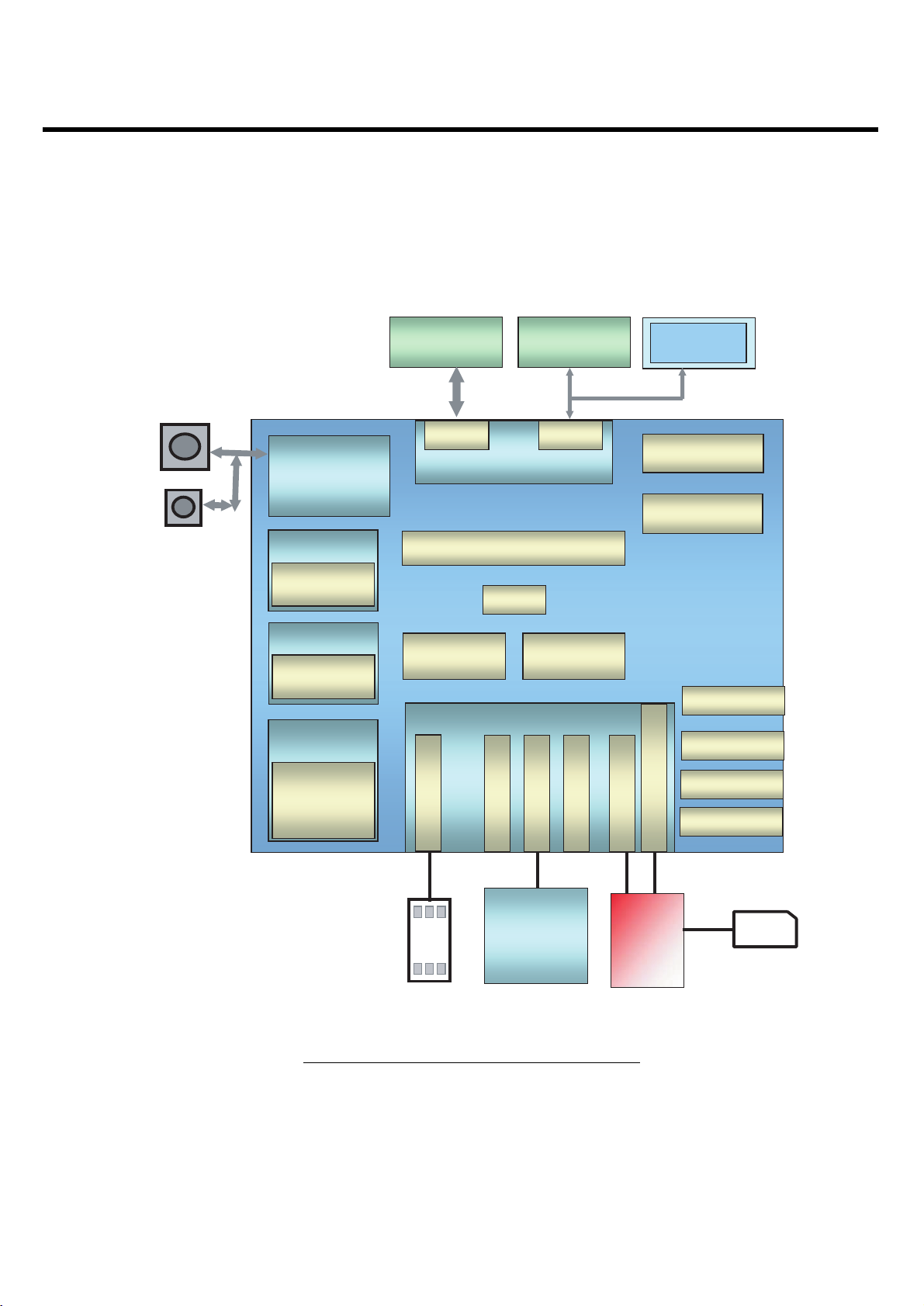
Figure. PM6650 Functional Block Diagram
LGE Internal Use Only
Copyright © 2008 LG Electronics. Inc. All right reserved.
Only for training and service purposes
3. TECHNICAL BRIEF
- 27 -
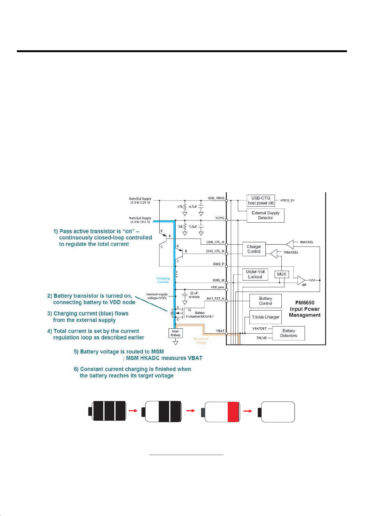
3.3.3. Charging control
A programmable charging block in PM6650 is used for battery charging. It is possible to set limits for
the charging current. The external supply typically connects directly to pin (VCHG). The voltage on this
pin (VCHG) is monitored by detection circuitry to ascertain whether a valid external supply is applied or
not. For additional accuracy or to capture variations over time, this voltage is routed internally to the
housekeeping ADC via the analog multiplexer. PM6650 circuits monitor voltages at VCHARGER and
ICHARGE pins to determine which supply should be used and when to switch between the two
supplies. These pins are connected to the Source (or emitter) and Drain (or collector) contacts of the
pass transistor respectively.
L852i Battery Bar Display
[Call]3.66V ± 0.05V
[Idle]3.72V ± 0.05V
[Call]3.56V ± 0.05V
[Idle]3.61V ± 0.05V
[Call & Idle]3.26 ± 0.05V
- 28 -
3. TECHNICAL BRIEF
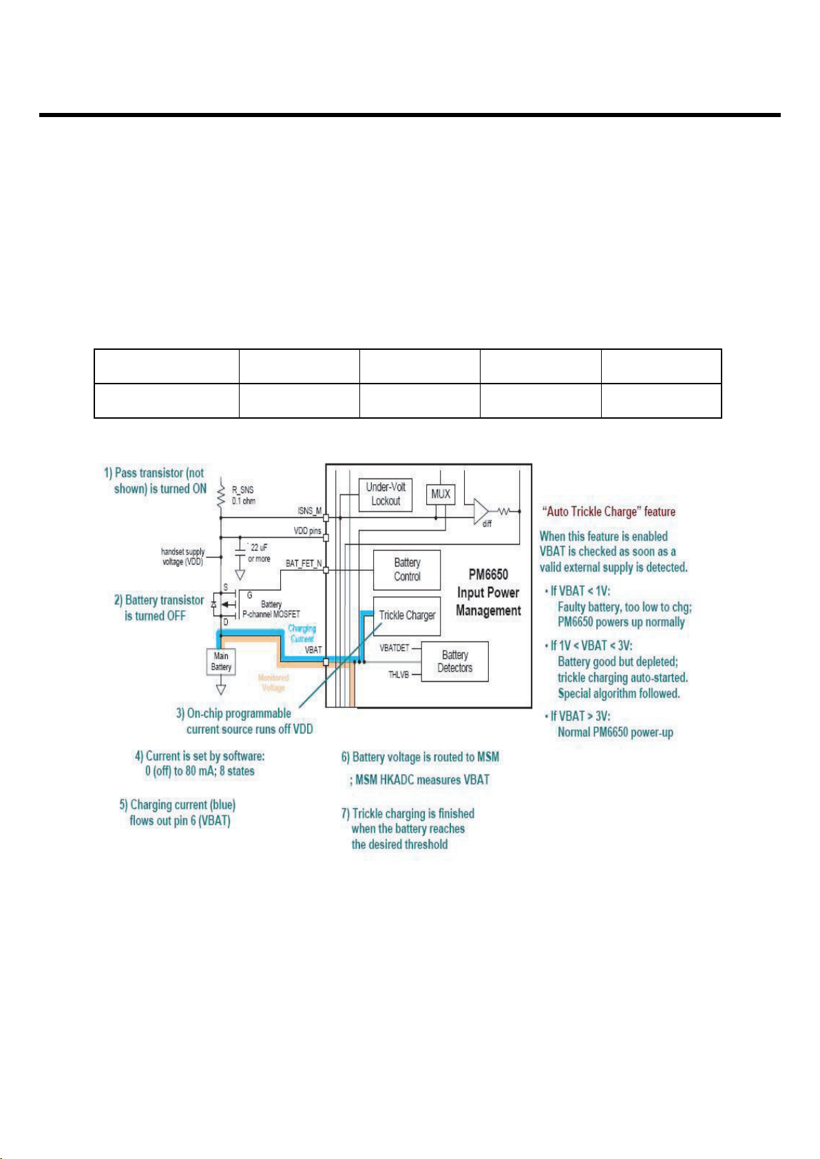
Trickle Charging
Trickle Charging of the main battery, enabled through SBI control and powered from VDD, is provided
by the PM6650 IC, The trickle charger is on-chip programmable current source that supplies current
from VDD to pin (VBAT). Trickle charging can be used for lithium-ion and nickelbased batteries, with
its performance specified below (3.2V). The charging current is set to 80mA.
LGE Internal Use Only
Copyright © 2008 LG Electronics. Inc. All right reserved.
Only for training and service purposes
Parameter Min Typ Max Unit
Trickle Current 60 80 100 mA

- 29 -
3. TECHNICAL BRIEF
Constant Current Charging
The PM6650 IC supports constant current charging of the main battery by controlling the charger pass
transistor and the battery transistor. The constant current charging continues until the battery reaches
its target voltage, 4.2V.
Constant Voltage Charging
Constant voltage charging begins when the battery voltage reaches a target voltage, 4.2V. The end of
constant voltage charging is commonly detected 10% of the full charging current (140mA)
• Charging Method : CC & CV (Constant Current & Constant Voltage)
• Maximum Charging Voltage : 4.2V
• Maximum Charging Current : 600mA
• Nominal Battery Capacity : 900 mAh
• Charger Voltage : 5.4V
• Charging time : Max 160min (Except time trickle charging)
• Full charge indication current (icon stop current) : 140mA
• Low battery message : 3.26 ± 0.05V
• Cut-off : [Idle] 60s after Low battery message
[Call] 80s after Low battery message
LGE Internal Use Only
Copyright © 2008 LG Electronics. Inc. All right reserved.
Only for training and service purposes

- 30 -
3. TECHNICAL BRIEF
3.4 External memory interface
A. MSM6280
The MSM6280 device was designed to provide two distinct memory interfaces. EBI1 was targeted for
supporting high speed synchronous memory devices. EBI2 was targeted towards supporting slower
asynchronous devices such as LCD, NAND flash, SRAM, etc.
• EBI1 Features
- 16 bit static and dynamic memory interface
- 32 bit dynamic memory interface
- 24 bits of address for static memory devices which can support up to 32MBytes on each chip select
- Synchronous burst memories supported (burst NOR, burst PSRAM)
- Synchronous DRAM memories supported
- Byte addressable memory supporting 8 bit, 16 bit and 32 bit accesses
- Pseudo SRAM (PSRAM) memory support
• EBI2 Features
- Support for asynchronous FLASH and SRAM(16bit & 8bit).
- Interface support for byte addressable 16bit devices(UB_N & LB_N signals).
- 2Mbytes of memory per chip select.
- Support for 8 bit/16bit wide NAND flash.
- Support for parallel LCD interfaces, port mapped of memory mapped(18 or 16 bit)
• 2Gb NAND(16bit) flash memory + 1Gb SDRAM (32bit)
• 1-CS(Chip Select) is used
LGE Internal Use Only
Copyright © 2008 LG Electronics. Inc. All right reserved.
Only for training and service purposes
Interface Spec
Device Part Name Maker Read Access Time Write Access Time
FLASH TYA000B800COGG Toshiba 50 ns 50 ns
SDRAM TYA000B800COGG Toshiba 15 ns 15 ns
Table#1. External memory interface for L852i
- 31 -
3. TECHNICAL BRIEF
3.5 H/W Sub System
3.5.1 RF Interface
A. RTR6275(WCDMA_Tx)
MSM6280 controls RF part(RTR6275) using these signals.
• SSBDT_RTR : SSBI I/F signals for control Sub-chipset
• RX_I/Q_M/P,TX_I/Q_M/P : I/Q for T/Rx of RF
• TX_AGC_ADJ : control the gain of the Tx signal prior to the power amplifier
B. RFR6275(WCDMA_Rx)
• SSBDT_RFR : SSBI I/F signals for control Sub-chipset
• RX_I/Q_M/P : I/Q for Rx of RF
C. the others
• TRK_LO_ADJ : TCXO(19.2M) Control
• PA_ON0 : WCDMA(800), WCDMA(2100) TX Power Amp Enable
• PA_ON1 : WCDMA(2100) TX Power Amp Enable
LGE Internal Use Only
Copyright © 2008 LG Electronics. Inc. All right reserved.
Only for training and service purposes
Figure. Schematic of RF Interface of MSM6280
Near to MSM
(WCMDA 2100PAM Enable)
TP201
33nF
C239
2KR210
SYNTH0_GP_PDM0_GPIO92
TCXO_EN_GPIO94
F19
TRK_LO_ADJ
L13
H13
TX_AGC_ADJ
Q_OUT_N
SBST1_GPIO93
H18
PA_ON0
F17
AA25
Q_IM_CH0
Q_IM_CH1
W23
Y25
Q_IP_CH0
Q_IP_CH1
V23
B12
Q_OUT
A12
A13
AB25
I_IM_CH0
V25
I_IM_CH1
AC25
I_IP_CH0
W25
I_IP_CH1
I_OUT
B13
I_OUT_N
F12
DAC_REF
AP_1.2V_EN
PA_ON0
TRK_LO_ADJ
TCXO_EN
DAC_REF
TX_QM
TX_QP
TX_IM
TX_IP
RX_QM
RX_QP
RX_IM
RX_IP
TX_AGC_ADJ
 Loading...