

LG KU580 Service Manual
Date: August, 2007 / Issue 1.0
Service Manual
Model : KU580
Service Manual
KU580
Internal Use Only

- 3 -
LGE Internal Use Only
Copyright © 2007 LG Electronics. Inc. All right reserved.
Only for training and service purposes
1. INTRODUCTION .............................. 5
1.1 Purpose................................................... 5
1.2 Regulatory Information............................ 5
2. PERFORMANCE.............................. 7
2.1 System Overview .................................... 7
2.2 Usable environment ................................ 8
2.3 Radio Performance ................................. 8
2.4 Current Consumption............................ 16
2.5 RSSI BAR ............................................. 16
2.6 Battery Bar ............................................ 17
2.7 Sound Pressure Level........................... 18
2.8 Charging ............................................... 19
3. Technical Brief .............................. 20
3.1 Digital Baseband(DBB) & Multimedia
Processor.............................................. 20
3.2 GAM Hardware Subsystem ...................41
3.3 Audio Part ..............................................51
3.4 GPADC(General Purpose ADC) and
AUTOADC2 ...........................................59
3.5 Charger control ......................................60
3.6 Voltage Regulation.................................66
3.7 RF Technical Description.......................67
4. TROUBLE SHOOTING ...................78
4.1 Power ON Trouble .................................78
4.2 USB Trouble ..........................................79
4.3 SIM Detect Trouble ................................80
4.4 MicroSD card Trouble ............................81
4.5 Keypad And Touch key Trouble.............82
4.6 Camera Trouble .....................................85
4.7 Main LCD Trouble..................................89
4.8 Keypad Backlight Trouble......................91
4.9 Folder ON/OFF Trouble .........................93
4.10 Audio Trouble Shooting .......................95
4.11 Charger Trouble Shooting..................110
4.12 Checking Bluetooth Block..................113
4.13 RF Component...................................117
4.14 Procedure to check............................118
4.15 Checking Common Power Source
Block ..................................................119
4.16 Checking VCXO Block .......................124
4.17 Checking Front End Module Block.....129
4.18 Checking Front End Module Block
input logic...........................................130
4.19 Checking WCDMA Block ...................133
4.20 Checking GSM Block .........................145
5. KU580 Download Setup Manual 157
6. BLOCK DIAGRAM ....................... 164
6.1 GSM & WCDMA RF Block...................164
7. CIRCUIT DIAGRAM ..................... 167
8. PCB LAYOUT................................175
9. CALIBRATION ..............................181
9.1 General Description .............................181
10. EXPLODED VIEW &
REPLACEMENT PART LIST ......187
10.1 EXPLODED VIEW .............................187
10.2 Replacement Parts ............................189
<Mechanic component> .................... 189
<Main component> ............................ 193
10.3 Accessory ......................................... 208
Table of Contents

- 4 -
LGE Internal Use Only
Copyright © 2007 LG Electronics. Inc. All right reserved.
Only for training and service purposes
Table Of Contents

- 5 -
LGE Internal Use Only
Copyright © 2007 LG Electronics. Inc. All right reserved.
Only for training and service purposes
Table Of Contents
1.1 Purpose
This manual provides the information necessary to repair, calibration, description and download the
features of this model.
1.2 Regulatory Information
A. Security
Toll fraud, the unauthorized use of telecommunications system by an unauthorized part (for example,
persons other than your company’s employees, agents, subcontractors, or person working on your
company’s behalf) can result in substantial additional charges for your telecommunications services.
System users are responsible for the security of own system.
There are may be risks of toll fraud associated with your telecommunications system. System users
are responsible for programming and configuring the equipment to prevent unauthorized use. The
manufacturer does not warrant that this product is immune from the above case but will prevent
unauthorized use of commoncarrier telecommunication service of facilities accessed through or
connected to it. The manufacturer will not be responsible for any charges that result from such
unauthorized use.
B. Incidence of Harm
If a telephone company determines that the equipment provided to customer is faulty and possibly
causing harm or interruption in service to the telephone network, it should disconnect telephone
service until repair can be done. A telephone company may temporarily disconnect service as long as
repair is not done.
C. Changes in Service
A local telephone company may make changes in its communications facilities or procedure. If these
changes could reasonably be expected to affect the use of the phones or compatibility with the net
work, the telephone company is required to give advanced written notice to the user, allowing the user
to take appropriate steps to maintain telephone service.
D. Maintenance Limitations
Maintenance limitations on the phones must be performed only by the manufacturer or its authorized
agent. The user may not make any changes and/or repairs expect as specifically noted in this manual.
Therefore, note that unauthorized alternations or repair may affect the regulatory status of the system
and may void any remaining warranty.
1. INTRODUCTION
- 6 -
LGE Internal Use Only
Copyright © 2007 LG Electronics. Inc. All right reserved.
Only for training and service purposes
1. INTRODUCTION
E. Notice of Radiated Emissions
This model complies with rules regarding radiation and radio frequency emission as defined by local
regulatory agencies. In accordance with these agencies, you may be required to provide information
such as the following to the end user.
F. Pictures
The pictures in this manual are for illustrative purposes only; your actual hardware may look slightly
different.
G. Interference and Attenuation
A phone may interfere with sensitive laboratory equipment, medical equipment, etc. Interference from
unsuppressed engines or electric motors may cause problems.
H. Electrostatic Sensitive Devices
ATTENTION
Boards, which contain Electrostatic Sensitive Device (ESD), are indicated by the sign.
Following information is ESD handling:
• Service personnel should ground themselves by using a wrist strap when exchange system boards.
• When repairs are made to a system board, they should spread the floor with anti-static mat which is
also grounded.
• Use a suitable, grounded soldering iron.
• Keep sensitive parts in these protective packages until these are used.
• When returning system boards or parts like EEPROM to the factory, use the protective package as
described.
- 7 -
LGE Internal Use Only
Copyright © 2007 LG Electronics. Inc. All right reserved.
Only for training and service purposes
2. PERFORMANCE
2.1 System Overview
2. PERFORMANCE
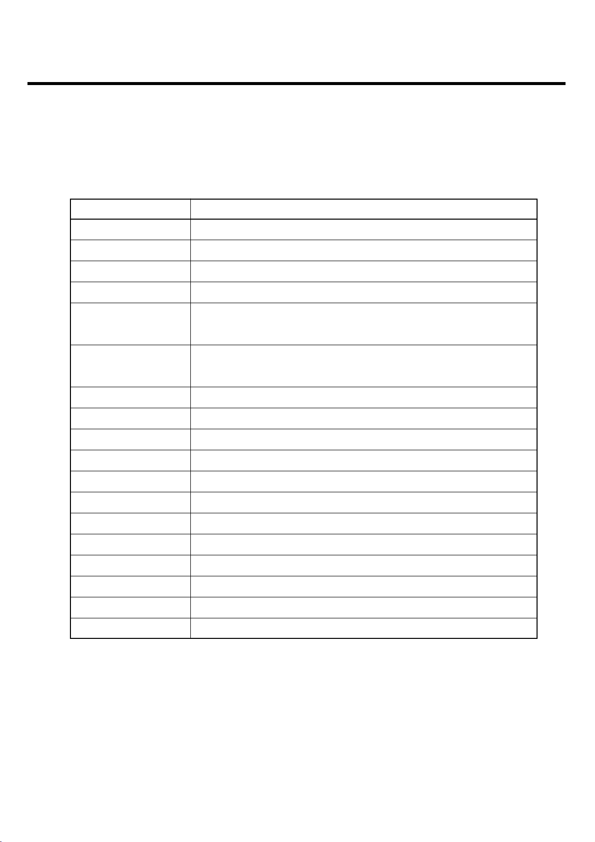
Item Specification
Shape GSM900/1800/1900 & WCDMA Slide type - Dual Mode Handset
Size 93.9X52.9X16.45 mm
Weight 100g (with standard battery)
Power 860mAh Li-Polymer
Talk Time Over 170 Min (WCDMA, Tx=12 dBm, Voice)
Over 200 Min (GSM, Tx=Max, Voice)
Standby Time Over 280 hrs (WCDMA, DRX=2.56)
Over 280 hrs (GSM, Paging period=5)
Antenna Intenna type
Main LCD 2.0"(320x240), 260K TFT Color LCD
Main LCD BL White LED Backlight
Vibrator Yes (Coin Type)
MIC Yes (SMD Type)
Receiver Yes
Earphone Jack Yes
SIM Socket Yes(SIM Block Type) : 3.0V & 1.8V
Volume Key Push Type ( + , - )
Voice Key Push Type
External Memory T - Flash Socket
I/O Connect 18 Pin
- 8 -
LGE Internal Use Only
Copyright © 2007 LG Electronics. Inc. All right reserved.
Only for training and service purposes
2. PERFORMANCE
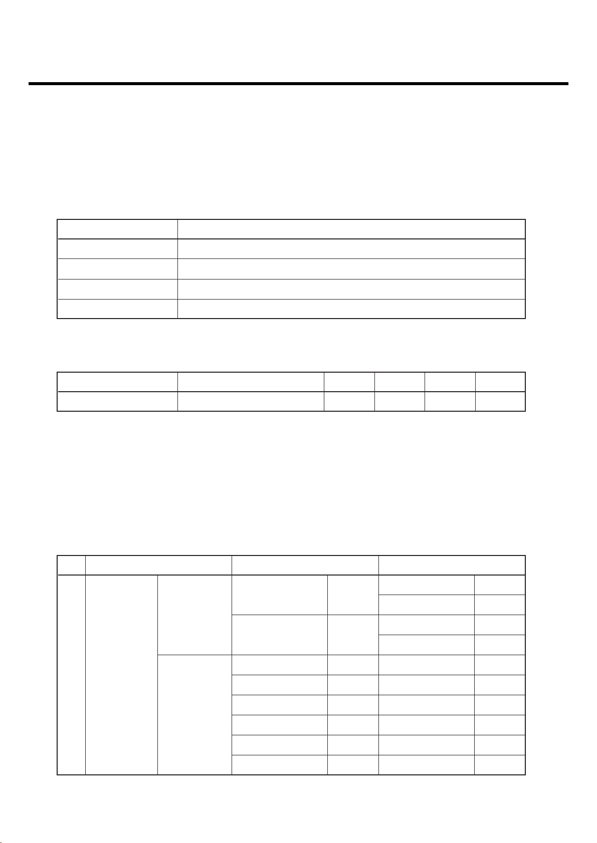
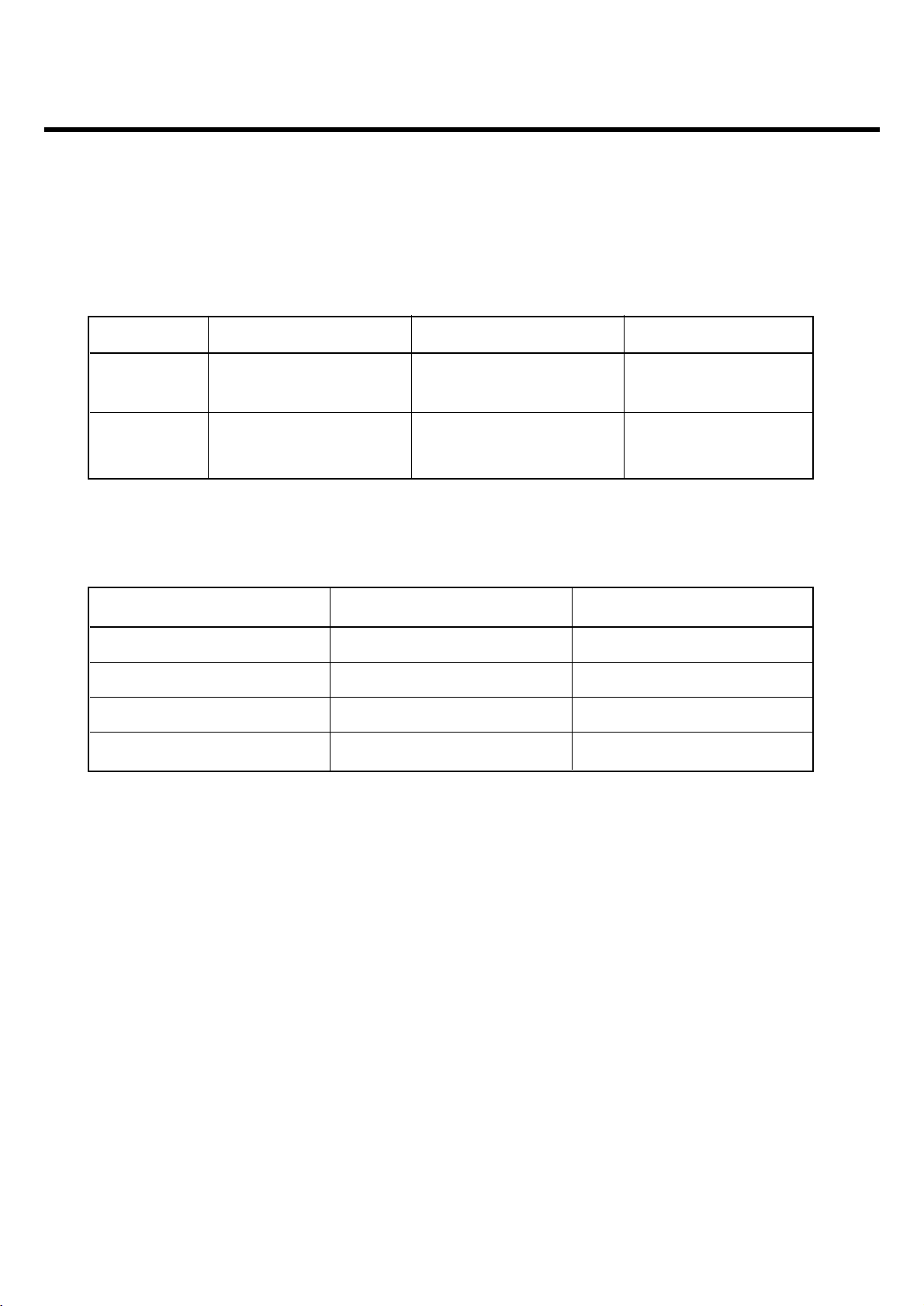
2.2 Usable environment
1) Environment
2) Environment(Accessory)
* CLA : 12~24V (DC)
2.3 Radio Performance
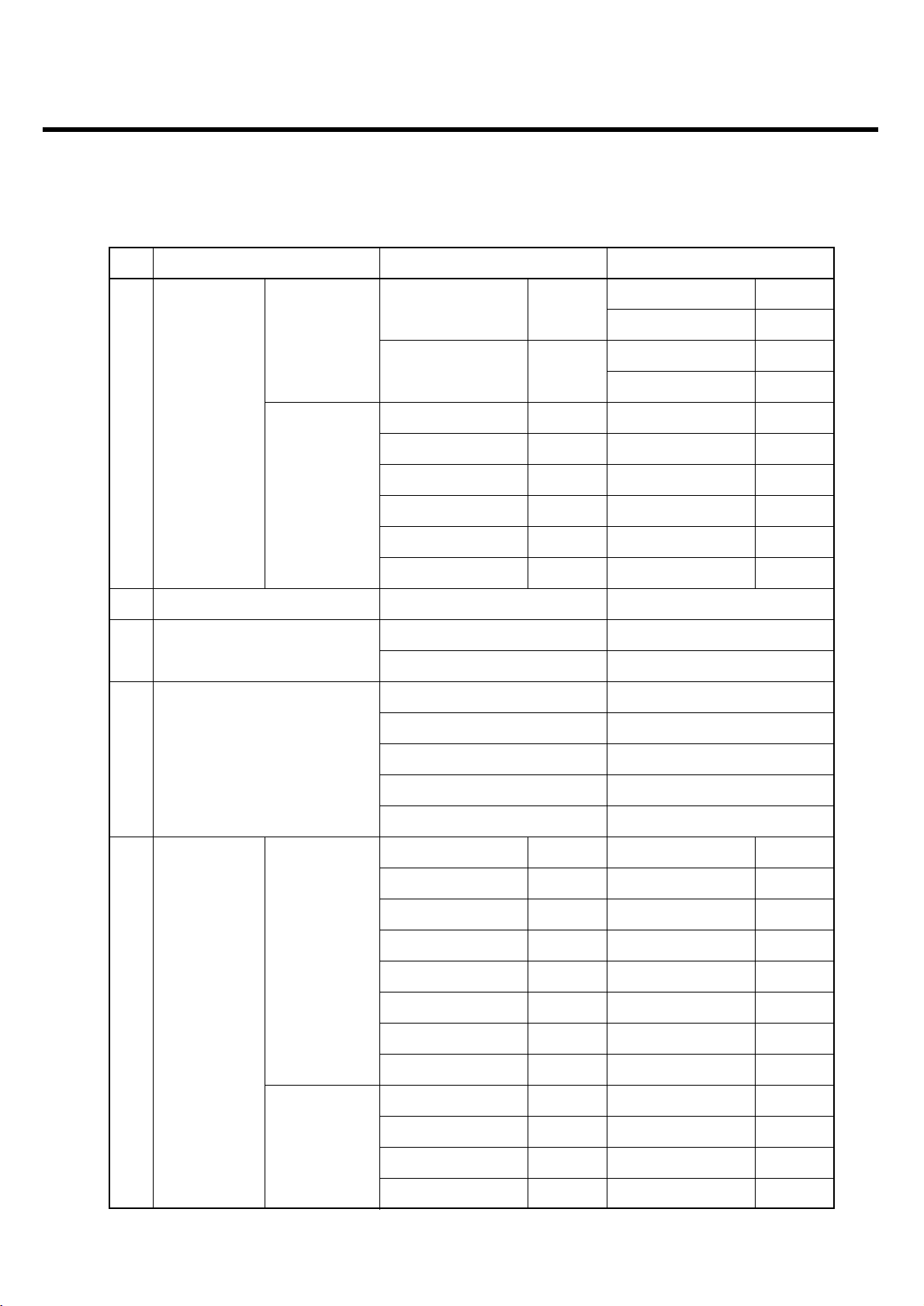
1) Transmitter - GSM Mode
Item Spec. Unit
Voltage 3.7 (Typ), 3.4 (Min), (Shut Down: 3.23) V
Operating Temp. -20 ~ +60 °C
Storage Temp. -30 ~ +85 °C
Humidity max. 85 %
Item Spec. Min Typ. Max Unit
Power Available power 100 220 240 Vac
No Item GSM DCS & PCS
100k~1GHz -39dBm
9k ~ 1GHz -39dBm
MS allocated 1G ~ 1710MHz -33dBm
Channel
1G~12.75GHz -33dBm
1710M ~ 1785MHz -39dBm
Conducted 1785M ~ 12.75GHz -33dBm
1 Spurious 100k~880MHz -60dBm 100k ~ 880MHz -60dBm
Emission 880M~915MHz -62dBm 880M ~ 915MHz -62dBm
Idle Mode
915M ~ 1000Mz -60dBm 915M ~ 1000MHz -60dBm
1G ~ 1.71GHz -50dBm 1G ~ 1.71GHz -50dBm
1.71G ~ 1.785GHz -56dBm 1.71G ~ 1.785GHz -56dBm
1.785G ~ 12.75GHz -50dBm 1.785G ~ 12.75GHz -50dBm
- 9 -
LGE Internal Use Only
Copyright © 2007 LG Electronics. Inc. All right reserved.
Only for training and service purposes
2. PERFORMANCE
No Item GSM DCS & PCS
30M ~ 1GHz -36dBm
30M~1GHz -36dBm
MS allocated 1G ~ 1710MHz -30dBm
Channel
1G ~ 4GHz -30dBm
1710M ~ 1785MHz -36dBm
Radiated 1785M ~ 4GHz -30dBm
2Spurious 30M ~ 880MHz -57dBm 30M ~ 880MHz -57dBm
Emission 880M ~ 915MHz -59dBm 880M ~ 915MHz -59dBm
Idle Mode
915M ~ 1000Mz -57dBm 915M ~ 1000MHz -57dBm
1G ~ 1.71GHz -47dBm 1G ~ 1.71GHz -47dBm
1.71G ~ 1.785GHz -53dBm 1.71G ~ 1.785GHz -53dBm
1.785G ~ 4GHz -47dBm 1.785G ~ 4GHz -47dBm
3 Frequency Error ±0.1ppm ±0.1ppm
4 Phase Error
±5(RMS) ±5(RMS)
±20(PEAK) ±20(PEAK)
3dB below reference sensitivity 3dB below reference sensitivity
Frequency Error RA250 : ±200Hz RA250: ±250Hz
5 Under Multipath and HT100 : ±100Hz HT100: ±250Hz
Interference Condition TU50 : ±100Hz TU50: ±150Hz
TU3 : ±150Hz TU1.5: ±200Hz
0 ~ 100kHz +0.5dB 0 ~ 100kHz +0.5dB
200kHz -30dB 200kHz -30dB
250kHz -33dB 250kHz -31dB
Due to 400kHz -60dB 400kHz -33dB
Output RF
modulation 600 ~ 1800kHz -66dB 600 ~ 1800kHz -60dB
6 1800 ~ 3000kHz -69dB 1800 ~ 6000kHz -60dB
Spectrum
3000 ~ 6000kHz -71dB ≥6000kHz -73dB
≥6000kHz -77dB
Due to
400kHz -19dB 400kHz -22dB
Switching
600kHz -21dB 600kHz -24dB
transient
1200kHz -21dB 1200kHz -24dB
1800kHz -24dB 1800kHz -27dB
- 10 -
LGE Internal Use Only
Copyright © 2007 LG Electronics. Inc. All right reserved.
Only for training and service purposes
2. PERFORMANCE
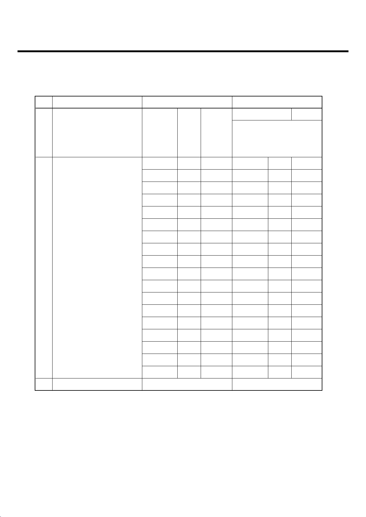
No Item GSM DCS & PCS
Frequency offset 800kHz
7 Intermodulation attenuation –
Intermodulation product should
be Less than 55dB below the
level of Wanted signal
Power control
Power Tolerance
Power control
Power Tolerance
Level (dBm) (dB) Level (dBm) (dB)
533±3 030±3
631±3 128±3
729±3 226±3
827±3 324±3
925±3 422±3
10 23 ±3 5 20 ±3
8 Transmitter Output Power 11 21 ±3 6 18 ±3
12 19 ±3 7 16 ±3
13 17 ±3 8 14 ±3
14 15 ±3 9 12 ±4
15 13 ±3 10 10 ±4
16 11 ±5 11 8 ±4
17 9 ±5 12 6 ±4
18 7 ±5 13 4 ±4
19 5 ±5 14 2 ±5
15 0 ±5
9 Burst timing Mask IN Mask IN
- 11 -
LGE Internal Use Only
Copyright © 2007 LG Electronics. Inc. All right reserved.
Only for training and service purposes
2. PERFORMANCE
2) Transmitter - WCDMA Mode
No Item Specification
1 Maximum Output Power Class 3 : +24dBm(+1/-3dB)
Class 4 : +21dBm(±2dB)
2 Frequency Error ±0.1ppm
3 Open Loop Power control in uplink ±9dB@normal, ±12dB@extreme
Adjust output(TPC command)
cmd 1dB 2dB 3dB
+1 +0.5/1.5 +1/3 +1.5/4.5
4 Inner Loop Power control in uplink 0 -0.5/+0.5 -0.5/+0.5 -0.5/+0.5
-1 -0.5/-1.5 -1/-3 -1.5/-4.5
Group (10 equel command group)
+1 +8/+12 +16/+24
5 Minimum Output Power -50dBm(3.84MHz)
Qin/Qout : PCCH quality levels
6 Out-of-synchronization handling of output power Toff@DPCCH/Ior : -22 -> -28dB
Ton@DPCCH/Ior : -24 -> -18dB
7 Transmit OFF Power -56dBm(3.84MHz)
8 Transmit ON/OFF Time Mask
±25us
PRACH,CPCH,uplinlk compressed mode
±25us
9 Change of TFC
Power varies according to the data rate
DTX : DPCH off
(minimize interference between UE)
10 Power setting in uplink compressed ±3dB(after 14slots transmission gap)
11 Occupied Bandwidth(OBW) 5MHz(99%)
-35-15*(∆f-2.5)dBc@∆f=2.5~3.5MHz,30k
12 Spectrum emission Mask
-35-1*(∆f-3.5)dBc@∆f=3.5~7.5MHz,1M
-39-10*(∆f-7.5)dBc@∆f=7.5~8.5MHz,1M
-49dBc@∆f=8.5~12.5MHz,1M
- 12 -
LGE Internal Use Only
Copyright © 2007 LG Electronics. Inc. All right reserved.
Only for training and service purposes
2. PERFORMANCE
3)Receiver - GSM Mode
No Item Specification
13 Adjacent Channel Leakage Ratio(ACLR)
33dB@5MHz, ACP>-50dBm
43dB@10MHz, ACP>-50dBm
-36dBm@f=9~150KHz, 1K BW
-36dBm@f=50KHz~30MHz, 10K BW
-36dBm@f=30MHz~1000MHz, 100K BW
14
Spurious Emissions -30dBm@f=1~12.5GHz, 1M BW
(*: additional requirement) -41dBm*@1893.5~1919.6MHz, 300k
-67dBm*@925~935MHz, 100k
-79dBm*@935~960MHz, 100k
-71dBm*@1805~1880MHz, 100k
15 Transmit Intermodulation
-31dBc@5MHz,Interferer -40dBc
-41dBc@10MHz, Interferer -40dBc
16 Error Vector Magnitude (EVM)
17.5%(>-20dBm)
(@12.2K, 1DPDCH+1DPCCH)
17 Transmit OFF Power
-15dB@SF=4.768Kbps, Multi-code
transmission
No Item GSM DCS & PCS
1
Sensitivity (TCH/FS Class II) -105dBm -105dBm
2
Co-Channel Rejection
C/Ic=7dB Storage -30 ~ +85
(TCH/FS Class II, RBER, TU high/FH)
3 Adjacent Channel 200kHz C/Ia1=-12dB C/Ia1=-12dB
Rejection 400kHz C/Ia2=-44dB C/Ia2=-44dB
Wanted Signal :-98dBm Wanted Signal :-96dBm
4
Intermodulation Rejection 1st interferer:-44dBm 1st interferer:-44dBm
2nd interferer:-45dBm 2nd interferer:-44dBm
5
Blocking Response Wanted Signal :-101dBm Wanted Signal :-101dBm
(TCH/FS Class II, RBER)
Unwanted Signal: Depend on freq. Unwanted Signal: Depend on freq.
- 13 -
LGE Internal Use Only
Copyright © 2007 LG Electronics. Inc. All right reserved.
Only for training and service purposes
2. PERFORMANCE
4) Receiver - WCDMA Mode
No Item Specification
1 Reference Sensitivity Level -106.7 dBm(3.84 MHz)
-25dBm(3.84MHz)
2 Maximum Input Level -44dBm/3.84MHz(DPCH_Ec)
UE@+20dBm output power(Class3)
3 Adjacent Channel Selectivity (ACS)
33dB
UE@+20dBm output power(Class3)
-56dBm/3.84MHz@10MHz
4In-band Blocking UE@+20dBm output power(Class3)
-44dBm/3.84MHz@15MHz
UE@+20dBm output power(Class3)
-44dBm/3.84MHz@f=2050~2095 and
2185~2230MHz, band a)
UE@+20dBm output power(class3)
-30dBm/3.84MHz@f=2025~2050 &
5 Out-band Blocking 2230~2255MHz, band a)
UE@+20dBm output power(class3)
-15dBm/3.84MHz@f=1~2025 &
2255~12500MHz, band a)
UE@+20dBm output power(class3)
6 Spurious Response
-44dBm CW
UE@+20dBm output power(class3)
-46dBm CW@10MHz &
7 Intermodulation Characteristic -46dBm/3.84MHz@20MHz
UE@+20dBm output power(class3)
-57dBm@f=9KHz~1GHz, 100k BW
8 Spurious Emissions -47dBm@f=1~12.75GHz, 1M
-60dBm@f=1920~1980MHz, 3.84MHz
-60dBm@f=2110~2170MHz, 3.84MHz
- 14 -
LGE Internal Use Only
Copyright © 2007 LG Electronics. Inc. All right reserved.
Only for training and service purposes
2. PERFORMANCE
5) Bluetooth Mode
5.1) Transmitter
No Item Specification
1 Out Power Class 2 : -6~4dBm
2 Power Density Power density < 20dBm per 100kHz EIRP
3 Power Control Option 2dB ≤ step size ≤ 8dB
4 TX Output Spectrum -Frequency range
fmax & fmin @ below the level of -30dBm
(100khz BW) within 2.4GHz~2.4835GHz
5 TX Output Spectrum -20dB Bandwidth ≤ 1MHz
6 Tx Output Spectrum -Adjacent channel Po
≤ -20dBm @ C/I = 2MHz
≤ -40dBm @ C/I ≥ 3MHz
140kHz ≤ delta f1 avg ≥ 175kHz
7 Modulation Characteristics delta f2max ≥ 115kHz at least 99.9% of all
deltaf2max delta f2avg/deata f1avg0.8
8 Init. Carrier Freq. Tolerance ≤ ± 75KHz
1 slot : ≤ ± 25kHz
9 Carrier Frequency Drift
3 slot : ≤ ± 40kHz
5 slot : ≤ ± 40kHz
Maximum drift rate ≤ 20KHz/50usec
Freq.Range Operating Standby
30MHz~1GHz -36dBm -57dBm
10 Out of Band Spurious Emissions Above 1GHz~12.75GHz -30dBm -47dBm
1.8~1.9GHz -47dBm -47dBm
5.15~5.3GHz -47dBm -47dBm
- 15 -
LGE Internal Use Only
Copyright © 2007 LG Electronics. Inc. All right reserved.
Only for training and service purposes
2. PERFORMANCE
5.2) Receiver
No Item Specification
1 Sensitivity single slot packets BER ≤ 0.1%@-70dBm
2 Sensitivity multi slot packets BER ≤ 0.1%@-70dBm
3 C/I performance BER ≤ 0.1%@ (Low,Mid,High Frequency)
2405MHz, 2441MHz, 2477MHz
Interference Ratio
Co-Channel interference, C/I co-channel 11dB
Adjacent(1MHz)interference, C/I 1MHz 0dB
Adjacent(2MHz)interference, C/I 2MHz -30dB
Adjacent(3MHz)interference, C/I ≥ 3MHz -40dB
Adjacent(3MHz)interference to in band -9dB
mirror frequency, C/I image ±1MHz -20dB
4Blocking Characteristic BER ≤ 0.1%@wanted signal -67dBm
interfering Signal Frequency Power Level
30MHz~2000MHz -10dBm
2000MHz~2400MHz -27dBm
2500MHz~3000MHz -27dBm
3000MHz~12.75GHz -10dBm
5 Intermodluation Performance BER ≤ 0.1%@wanted signal -64dBm
static sinwave signal at f1=-39dBm
a BT modulated signal f2=-39dBm(payload PRBS15)
6 Maximum Input Level BER ≤ 0.1%@-20dBm
- 16 -
LGE Internal Use Only
Copyright © 2007 LG Electronics. Inc. All right reserved.
Only for training and service purposes
2. PERFORMANCE
2.4 Current Consumption
(VT test : Speaker off, LCD backlight On)
2.5 RSSI BAR
Stand by Voice Call VT
WCDMA
280 Hours = 3.0 mA 170 Min = 300 mA 110 Min= 450 mA
(DRX=2.56) (Tx=12dBm) (Tx=12dBm)
280 Hours = 3.0 mA 200 Min = 250 mA
GSM
(paging=5period) (Tx=Max)
GSM WCDMA
BAR 4 → 3 -91 ± 2 dBm -87 ± 2 dBm
BAR 3 → 2 -96 ± 2 dBm -97 ± 2 dBm
BAR 2 → 1 -101 ± 2 dBm -107 ± 2 dBm
BAR 1 → 0 -106 ± 2 dBm -112 ± 2 dBm
- 17 -
LGE Internal Use Only
Copyright © 2007 LG Electronics. Inc. All right reserved.
Only for training and service purposes
2. PERFORMANCE
2.6 Battery Bar
Indication Standby
BAR 4 → 3 (72%) 3.89 ± 0.05V
BAR 3 → 2 (53%) 3.79 ± 0.05V
BAR 2 → 1 (28%) 3.71 ± 0.05V
BAR 1 → Icon Blinking (7%) 3.61 ± 0.05V
Low voltage, 3.54 ±0.05V(Talk: 1min. interval) -3%
warning message 3.54 ±0.05V(Standby: 3min. Inverval) -3%
Power OFF 3.10 ±0.05V ↓ (WCDMA Talk)
3.20 ±0.05V ↓ (else)
- 18 -
LGE Internal Use Only
Copyright © 2007 LG Electronics. Inc. All right reserved.
Only for training and service purposes
2. PERFORMANCE
2.7 Sound Pressure Level
No Test Item Specification
1 Sending Loudness Rating (SLR)
NOM
8±3dB
MAX
2 Receiving Loudness Rating (RLR)
NOM -1±3dB
MAX -15±3dB
3 Side Tone Masking Rating (STMR)
NOM
17dB over
MAX
4 Echo Loss (EL)
NOM
40dB over
MAX
5 Sending Distortion (SD) refer to TABLE 30.3
6 Receiving Distortion (RD) refer to TABLE 30.4
7 Idle Noise-Sending (INS)
NOM
-64dBm0p under
MAX
8 Idle Noise-Receiving (INR)
NOM -47dBPA under
MAX -36dBPA under
9 Sending Loudness Rating (SLR)
NOM
8±3dB
MAX
10 Receiving Loudness Rating (RLR)
NOM -1±3dB
MAX -12±3dB
11 Side Tone Masking Rating (STMR)
NOM
25dB over
MAX
12 Echo Loss (EL)
NOM
40dB over
MAX
13 Sending Distortion (SD) refer to TABLE 30.3
14 Receiving Distortion (RD) refer to TABLE 30.4
15 Idle Noise-Sending (INS)
NOM
-55dBm0p under
MAX
16 Idle Noise-Receiving (INR)
NOM -45dBPA under
MAX -40dBPA under
TDMA NOISE
GSM
SEND
–.GSM: Power Level: 5
MS
REV.
DCS: Power Level: 0
DCS
SEND
17
(Cell Power: -90 ~ -105dBm) REV.
-62dBm under
–.Acoustic(Max Vol.)
GSM
SEND
MS/HEADSET SLR: 8±3dB
Headset
REV.
MS/HEADSET RLR: -13±1dB/-15dB
DCS
SEND
(SLR/RLR: mid-Value Setting) REV.
A
C
O
U
S
T
I
C
MS
HEAD
SET

- 19 -
LGE Internal Use Only
Copyright © 2007 LG Electronics. Inc. All right reserved.
Only for training and service purposes
2. PERFORMANCE
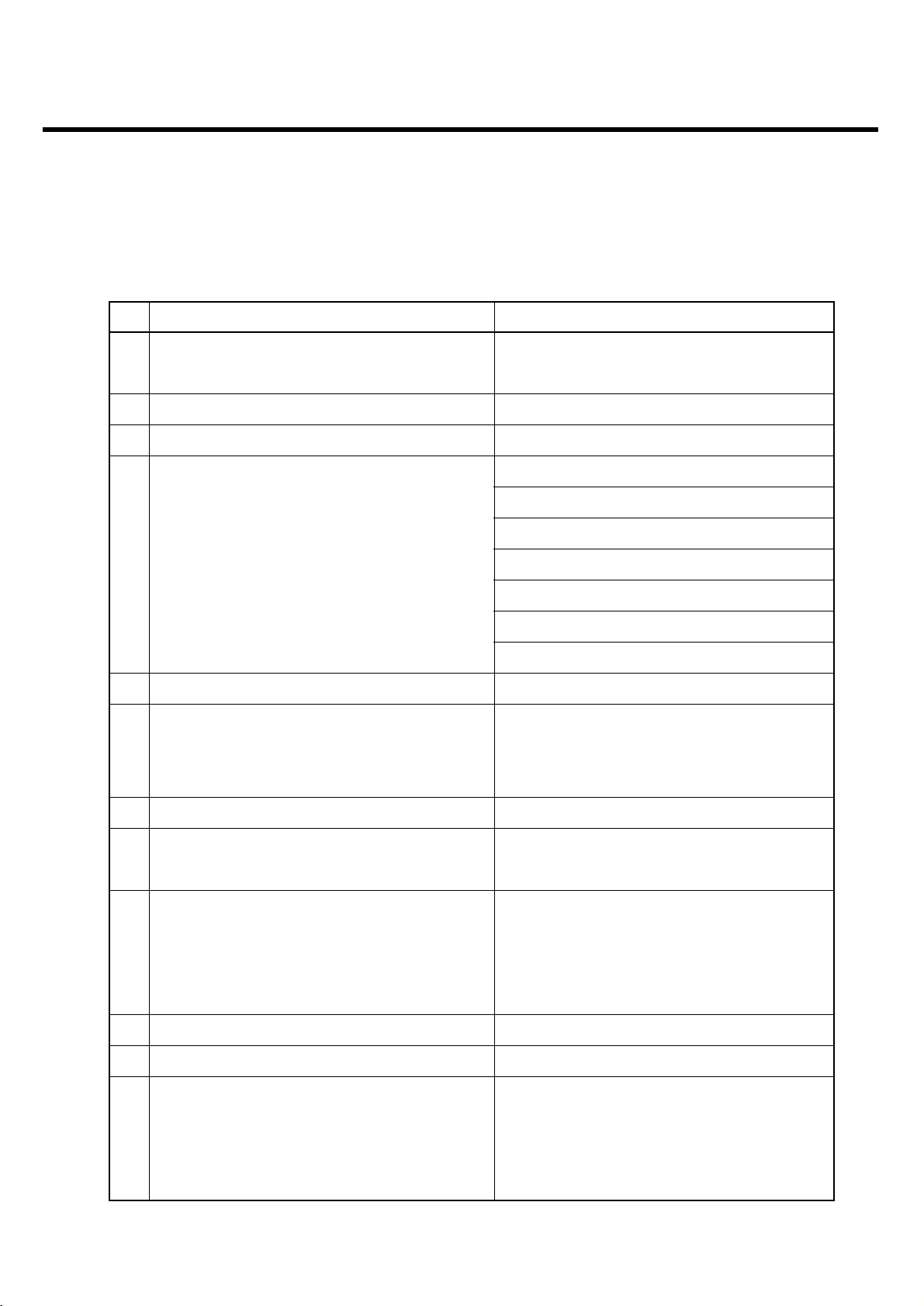
2.8 Charging
• Normal mode: Complete Voltage: 4.2V
Charging Current: 500mA
• Await mode: In case of During a Call, should be kept 3.9V
(GSM: It should be kept 3.9V in all power level WCDMA: It will not be kept 3.9V in
some power level)
• Extend await mode: At Charging prohibited temperature(0˚C under or 45˚C over)
(GSM: It should be kept 3.7V in all power level WCDMA: It will not be kept 3.7V
in some power level)

- 20 -
3. Technical Brief
LGE Internal Use Only
Copyright © 2007 LG Electronics. Inc. All right reserved.
Only for training and service purposes
3. BB Technical Description
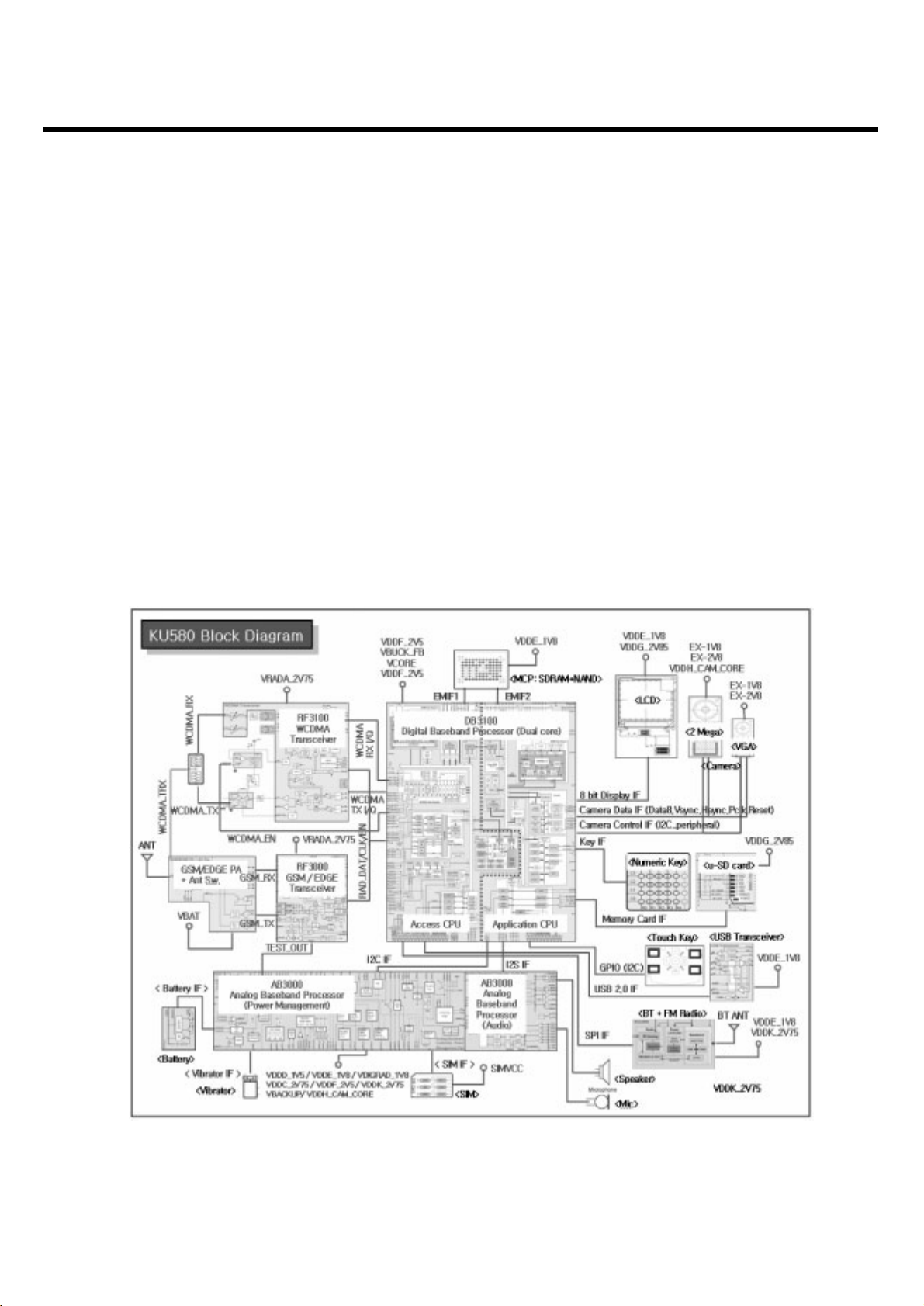
3.1 Digital Baseband(DBB) & Multimedia Processor
3.1.1 General Description
• Access subsystem
- Access Central Processing Unit (CPU) subsystem - ARM926, Joint Test Action Group (JTAG),
Embedded Trace Module (ETM), Instruction and Data (I&D)-cache, and I&DTCM
- Access peripheral subsystems - Subscriber Identity Module (SIM) interface, IrDA®, Universal Serial
Bus (USB), Universal Asynchronous Receiver/Transmitter (UART), and so on
- Digital Signal Processor (DSP) subsystem - CEVA-X1620, JTAG, Static Random Access Memory
(SRAM), and Program Data Read Only Memory (PDROM)
- EDGE/GSM/GPRS (EGG) subsystem - EGG hardware accelerators
- WCDMA subsystem - WCDMA hardware accelerators
• Application subsystem
- Application CPU subsystem - containing ARM926, JTAG, ETM, I&D-cache, and I&D-TCM
- Application peripheral subsystems - I2C™, keypad, UART, and so on
- Graphics subsystem - XGAM subsystem
- Audio Processing Execution (APEX) and video encoder subsystems In addition to the two
subsystems above, there is also a test block, chip control block, and a pad multiplexing block
residing at the top level
• DSP
- The Digital Signal Processor Subsystem (DSPSUB) includes a DSP megacell, which contains the
DSP CPU together with a tightly coupled memory. The DSP is the Ceva-X 1620 core with a 64 kB
instruction RAM and a 64 kB data RAM. It also contains debug logic and interfaces. In addition to
the megacell, the DSPSUB includes external memories, peripheral units, and interfaces. The DSP
megacell is clocked at 208 MHz.
- The DSPSUB includes an AHB master and an AHB slave interface. The AHB master provides a
direct access to the Internal Random Access Memory (IRAM) in the EGG core through the AHB.
The AHB slave interface allows the CPU and the DMA to access in the program and data RAM
residing in the DSPSUB.
• WCDMA subsystem
- The digital baseband controller WCDMA subsystem incorporate a WCDMA modem
- An interface to the WCMDA together with memory control and an internal single port RAM. The
WCDMA subsystem has three AHB slave interfaces.
- The Ericsson DB 3150 also includes HSDPA class 6 functionality.
- The WCDMA subsystem is handled and provided by Ericsson.
- 21 -
3. Technical Brief
LGE Internal Use Only
Copyright © 2007 LG Electronics. Inc. All right reserved.
Only for training and service purposes
• XGAM subsystem
- The XGAM subsystem is a graphics acceleration module that provides hardware support in the
creation of visual imagery and the transfer of this data to a display. The XGAM also provides
support for connecting a Camera module. The visual data could be graphics, still images, or video.
- The XGAM subsystem is handled and provided by Ericsson.
• Operation and Services
- I
2
C™ Interface
- SIM Interfaces
- General Purpose I/O (GPIO) Interface
- External Memory Interface that supports NAND, NOR, PSRAM, SDRAM,
- JTAG
- RTC
- ETM (in Prototype Package)
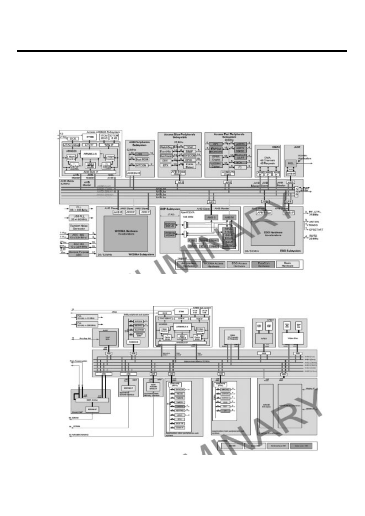
Figure 3-1-1 KU580 Block Diagram
- 22 -
LGE Internal Use Only
Copyright © 2007 LG Electronics. Inc. All right reserved.
Only for training and service purposes
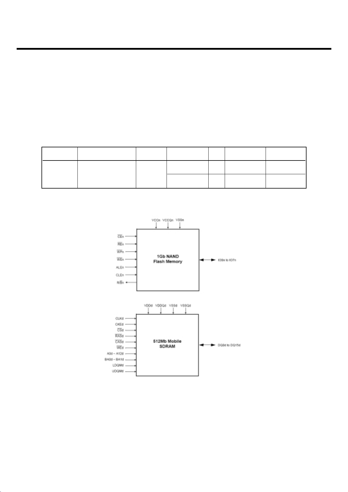
3.1.2 External memory interface
RF calibration data, Audio parameters and battery calibration data etc are stored in flash memory
area.
A. KU580
• 1Gb NAND flash memory + 512Mb SDRAM
• Data Communication
- IrDA ® (SIR)
- UARTs (ACB, EDB (RS232))
- Slave USB
• Package
- 12 by 12 mm 344 balls, 0.5mm pitch FPBGA Production Package
3. Technical Brief
Device Part Name Maker Item Time Size Speed
NAND flash K5D1G12ACB-D075 Samsung
Program speed 200µs 1 page = 528 Byte 2.64MByte/s
Erase speed 2ms 1 Block = 16K Byte 8MByte/s
Table 3- 1- 1. External Memory Interface Spec. of KU580
Figure 3- 1- 2. External Memory Configuration of KU580
- 23 -
3. Technical Brief
LGE Internal Use Only
Copyright © 2007 LG Electronics. Inc. All right reserved.
Only for training and service purposes
3.1.3 Hardware Architecture
A. Block Diagram
Figure 3-1-3. Access system of Ericsson DB3100
Figure 3-1-4. Application system of Ericsson DB3100

- 24 -
3. Technical Brief
LGE Internal Use Only
Copyright © 2007 LG Electronics. Inc. All right reserved.
Only for training and service purposes
B. CPU Subsystem
• Access CPU subsystem
The digital baseband controller includes an access CPU subsystem, which includes the submodules
described below.
− 32 KiB I-cache
− 16 KiB D-cache
− Page table
− Memory Management Unit (MMU)
− JTAG
− ETM9
− 26 KiB I-TCM
− 8 KiB D-TCM
• Application CPU subsystem
The digital baseband controller includes an Application CPU subsystem, which includes the
submodules described below.
− 32 KiB I-cache
− 16 KiB D-cache
− Page table
− MMU
− JTAG
− ETM9
− 8 KiB I-TCM
− 8 KiB D-TCM
C. Peripheral Hardware Subsystem
The digital baseband controller includes hardware that supports mobile terminal peripherals such as a
MMC, SD, UART, I2C, USB, keypad, and infrared. Collectively, this hardware comprises the
Peripheral subsystem.
The functional blocks of the Peripheral subsystem connect to the peripheral bus through four separate
bridges, which provide a simple interface to support different timing and memory access
arrangements.
D. DSP Hardware Subsystem
The Digital Signal Processor Subsystem (DSPSUB) includes a DSP megacell, which contains the DSP
CPU together with a tightly coupled memory. The DSP is the Ceva-X 1620 core with a 64 kB
instruction RAM and a 64 kB data RAM. It also contains debug logic and interfaces. In addition to the
megacell, the DSPSUB includes external memories, peripheral units, and interfaces. The DSP
megacell is clocked at 208 MHz.
The DSPSUB includes an AHB master and an AHB slave interface. The AHB master provides a direct
access to the Internal Random Access Memory (IRAM) in the EGG core through the AHB. The AHB
slave interface allows the CPU and the DMA to access in the program and data RAM residing in the
DSPSUB.
- 25 -
3. Technical Brief
LGE Internal Use Only
Copyright © 2007 LG Electronics. Inc. All right reserved.
Only for training and service purposes
E. XGAM Subsystem
The XGAM subsystem is a graphics acceleration module that provides hardware support in the
creation of visual imagery and the transfer of this data to a display. The XGAM also provides support
for connecting a Camera module. The visual data could be graphics, still images, or video.
The XGAM subsystem is handled and provided by Ericsson.
F. System Control Subsystem
The SYSCON resides at the top level of the circuit architecture and is responsible for clock generation
and clock and reset distribution within the digital baseband controller, as well as to external devices.
The block is a slave peripheral under control of the ARM processor. The programming of the SYSCON
controls the fundamental modes of operation within the digital baseband controller. Individual blocks
can also be reset and their clocks held inactive by accessing the appropriate control registers.
3.1.4 RF Interface
A. Asta Interface
Asta controls GSM RF part using these signals through GSM RF chip-Gimli.
• RF_DATA_A
• RF_DATA_B
• RF_DATA_C
• RF_DATA_STRB
B. WCDMA Radio Link Interface
• RF_WCDMA_PA_0_EN
• RF_WCDMA_PA_1_EN
• RF_WCDMA_DCDC_EN
• RF_WCDMA_PWRDET_EN
Figure 3-1- 5. Schematic of Asta RF Interface
Figure 3-1-6. Schematic of WCDMA RF Interface
Y4
RF_DATA_A
RF_DATA_B
AA2
Y3
RF_DATA_C
Y2
RF_DATA_STRB
QDATA_AMP_MSB
IDATA_FREQ_MSB
AMP_LSB_FREQ_LSB
DCLK_DATSTR
TX_POW
AB7
AB5
RF_WCDMA_DCDC_EN
AB8
RF_WCDMA_PA_0_EN
RF_WCDMA_PA_1_EN
V7
RF_WCDMA_PWRDET_EN
AB6
Y8
DAC_I_NEG
DAC_I_POS
W8
W7
DAC_Q_NEG
DAC_Q_POS
Y7
Y10
ADC_I_NEG
ADC_I_POS
W10
W9
ADC_Q_NEG
ADC_Q_POS
Y9
TP300
WPOW_DET
WDCDC_EN
WPA0_EN
WPOW_DET_EN
WTX_I_N
WTX_I_P
WTX_Q_N
WTX_Q_P
WRX_I_N
WRX_I_P
WRX_Q_N
WRX_Q_P
- 26 -
3. Technical Brief
LGE Internal Use Only
Copyright © 2007 LG Electronics. Inc. All right reserved.
Only for training and service purposes
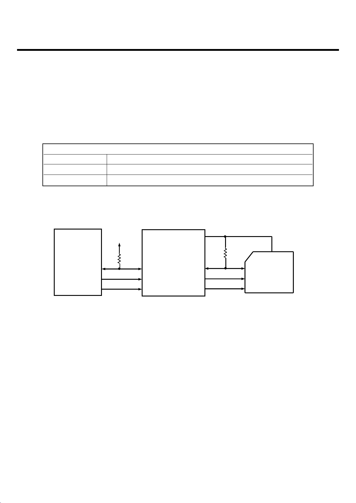
3.1.5 SIM Interface
SIM interface scheme is shown in Figure3-1-6.
SIMDAT0, SIMCLK0, SIMRST0 ports are used to communicate DBB(Asta) with
ABB(Veronica) and filter.
SIM (Interface between DBB and ABB)
SIMDAT0 SIM card bidirectional data line
SIMCLK0 SIM card reference clock
SIMRST0 SIM card async/sync reset
Table 3-1-2. SIM Interface
VDD
DAT
CLK CARD
RST
SIMVCC
Veronica
SDAT SIMDAT
SCLK SIMCLK
SRST SIMRST
Asta
SIMDAT0
SIMCLK0
SIMRST0
VDD
E
10K
10K
Figure 3-1-7. SIM Interface
- 27 -
3. Technical Brief
LGE Internal Use Only
Copyright © 2007 LG Electronics. Inc. All right reserved.
Only for training and service purposes
3.1.6 UART Interface
UART signals are connected to Asta GPIO through IO connector
UART0
Resource Name Note
ACC_GPIO_2 ACC_UART_RX ACC Receive Data
ACC_GPIO_3 ACC_UART_TX ACC Transmit Data
UART1
APP_GPIO_0 APP_UART_RX APP Receive Data
APP_GPIO_1 APP_UART_TX APP Transmit Data
Table 3- 1- 3. UART Interface
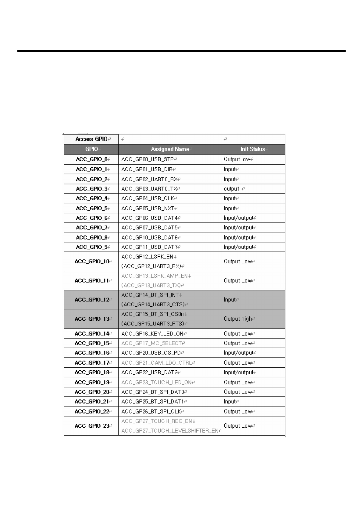
3.1.7 GPIO (General Purpose Input/Output) map
In total 39 allowable resources. This model is using 39 resources.
GPIO Map, describing application, I/O state, and enable level are shown in below table.
- 28 -
3. Technical Brief
LGE Internal Use Only
Copyright © 2007 LG Electronics. Inc. All right reserved.
Only for training and service purposes
Table 3-1-4. Asta ACC GPIO Map Table
- 29 -
LGE Internal Use Only
Copyright © 2007 LG Electronics. Inc. All right reserved.
Only for training and service purposes
3. Technical Brief
3.1.8 GPIO (General Purpose Input/Output) map
The USB block supports the implementation of a "full-speed" device fully compliant to USB 2.0
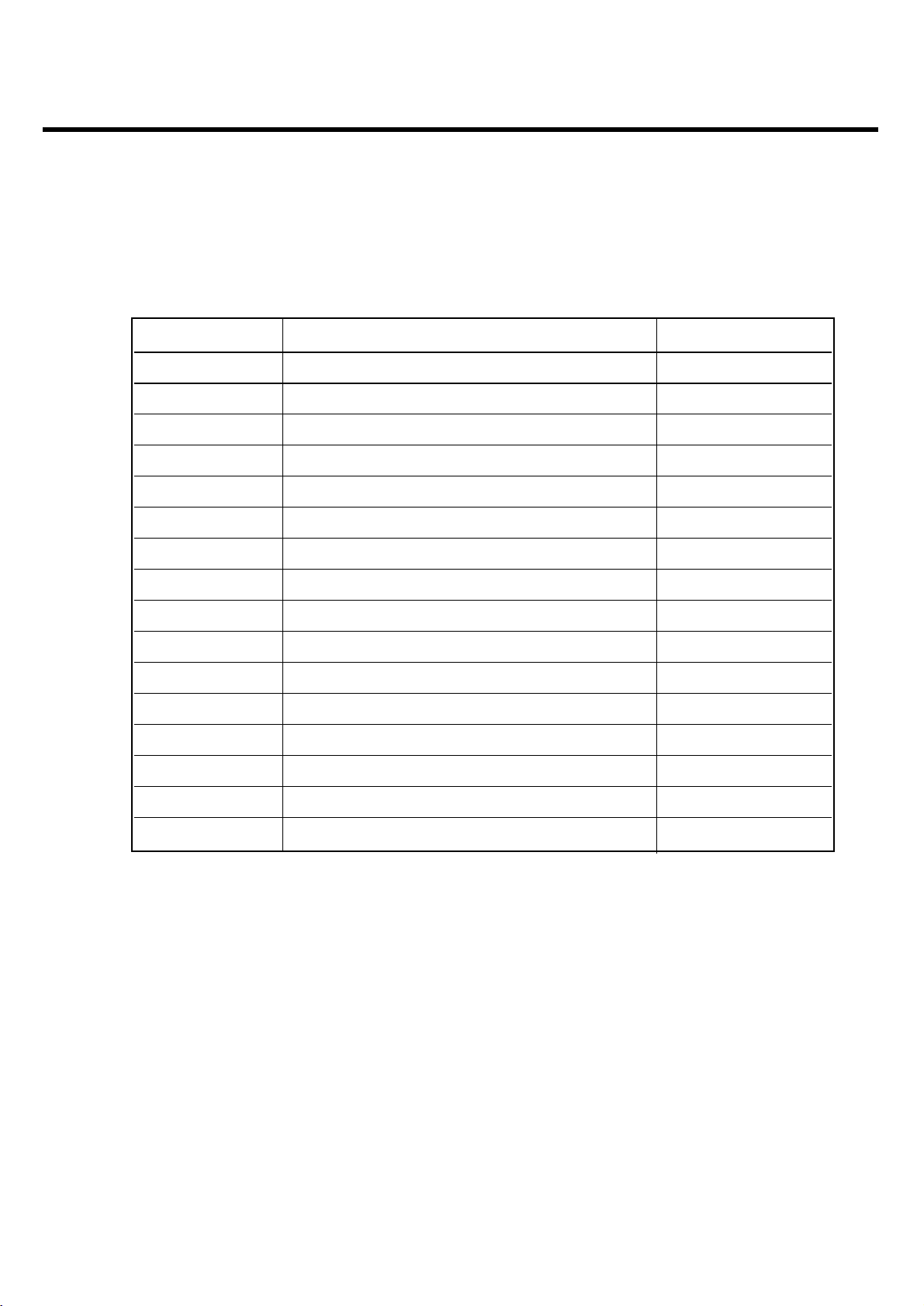
Access GPIO
GPIO Assigned Name Init Status
APP_GPIO_0 APP_GP00_UART_RX Input
APP_GPIO_1 APP_GP01_UART_TX Output
APP_GPIO_2 APP_GP02_FLIPSENSE Input
APP_GPIO_3 APP_GP03_HEAD_AMP_EN Output low
APP_GPIO_4 APP_GP04_FM_GPI02 Input
APP_GPIO_5 APP_GP05_TOUCH_ACK Input
APP_GPIO_6 APP_GP06_VC_IO_OFF Output Low(Hi-Z: low)
APP_GPIO_7 APP_GP07_VC_IO_OFF Output Low(Hi-Z: low)
APP_GPIO_8 APP_GP10_BL_CTRL output Low
APP_GPIO_9 APP_GP11_REMOTE_INT Input
APP_GPIO_10 APP_GP12_PHFSENSE Input
APP_GPIO_11 APP_GP13_MC_CLKRET Input
APP_GPIO_12 APP_GP14_MC_DETECT Input
APP_GPIO_13 APP_GP15_TOUCH_CLK Input/output
APP_GPIO_14 APP_GP16_TOUCH_DAT Input/output
- 30 -
3. Technical Brief
LGE Internal Use Only
Copyright © 2007 LG Electronics. Inc. All right reserved.
Only for training and service purposes
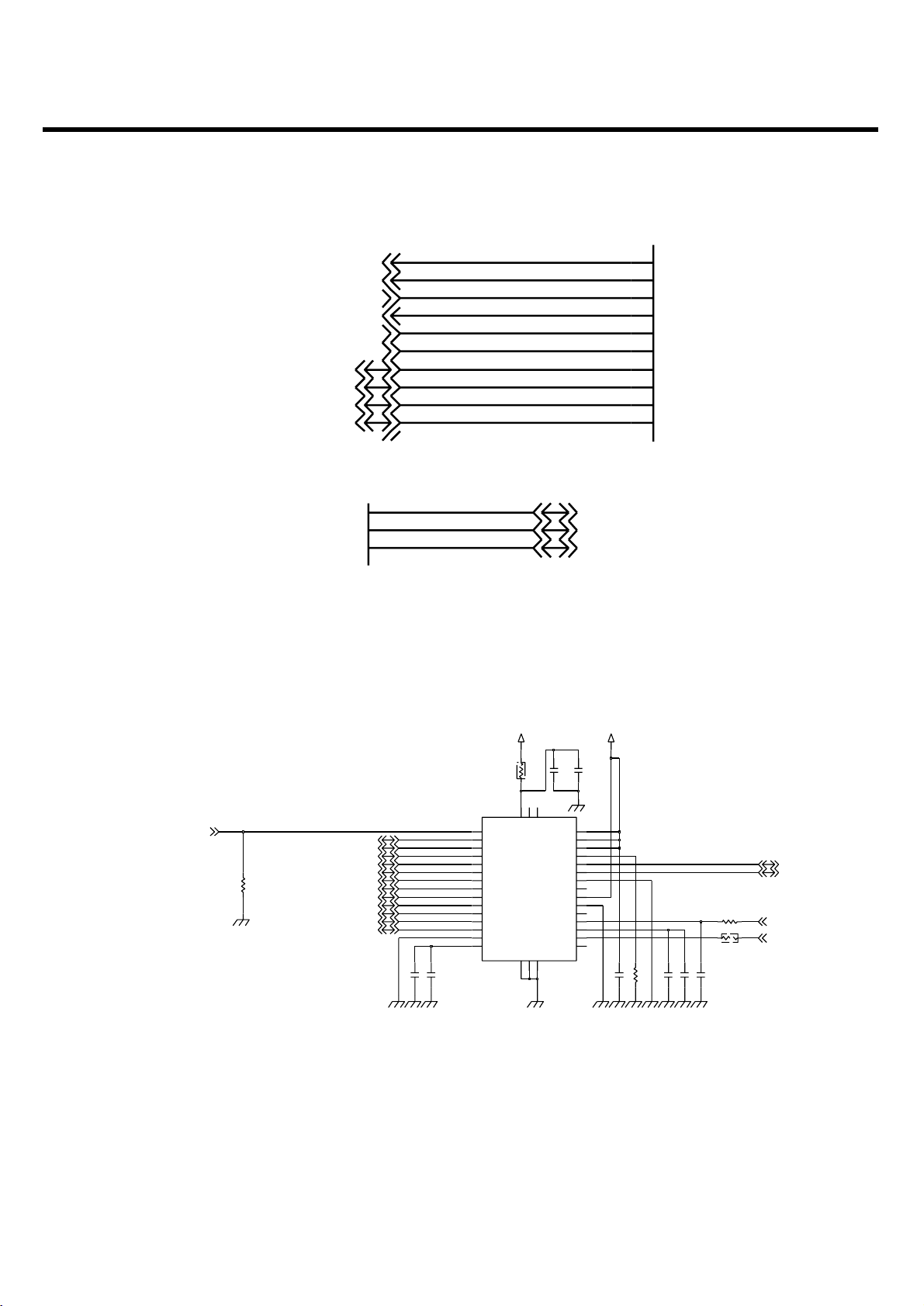
3.1.9 USB
The USB block supports the implementation of a “High-speed" device fully compliant to USB 2.0
standard. It provides an interface between the CPU (embedded local host) and the USB wire, and
handles USB transactions with minimal CPU intervention.
The USB specification allows up to 15 pairs of endpoints. Data for each endpoint is buffered in RAM
within the USB block and is read/written from the endpoint FIFO using DMA transfers or FIFO register
access. High-speed (high throughput) endpoints can use DMA while slower endpoints can use FIFO
register access.
The USB block can request up to six DMA channels, three for IN endpoints and three for OUT
endpoints.
USB Function Note
USB_STP ULPI stop signal
USB_DIR ULPI direction signal
USB_CLK USB clock
USB_NXT ULPI next signal
USB_DAT0 USB data0
USB_DAT1 USB data1
USB_DAT2 USB data2
USB_DAT3 USB data3
USB_DAT4 USB data4
USB_DAT5 USB data5
USB_DAT6 USB data6
USB_DAT7 USB data7
USB_CS_PD USB chip select
VBUS Power supply for Asta USB block
Table 3-1-6. USB Signal Interface of Asta
- 31 -
3. Technical Brief
LGE Internal Use Only
Copyright © 2007 LG Electronics. Inc. All right reserved.
Only for training and service purposes
Figure 3-1-8. Schematic of Asta USB block
Figure 3-1-9. Schematic of USB Transceiver
ACC_GPIO_6
P3
ACC_GPIO_7
P4
R4
ACC_GPIO_8
ACC_GPIO_9
R3
P2
ACC_GPIO_2
ACC_GPIO_3
N9
M9
ACC_GPIO_4
ACC_GPIO_5
N4
J9
ACC_GPIO_0
ACC_GPIO_1
K9
R2
ACC_GP07_USB_DAT5
ACC_GP06_USB_DAT4
ACC_GP10_USB_DAT6
ACC_GP11_USB_DAT7
ACC_GP00_USB_STP
ACC_GP01_USB_DIR
ACC_GP02_UART0_RX
ACC_GP03_UART0_TX
ACC_GP04_USB_CLK
ACC_GP05_USB_NXT
10V
1%
R438 12K
C429 0.1u
R435 51K
C433 2.2u
R436 1K
0.1uC431
4.7u
R437 0
4.7u
C424
C432
VBUS
VCC
F3
B5
VCC_IO1
VCC_IO2
B2
F5
XTAL1
XTAL2
F6
VDDE_1V8
C430 0.1u
C1
D1
DP
FAULT
E2
GND1
C5
D2
GND2
GND3
E4
D3
ID
NC1
F1
F2
NC2
D5
NXT PSW_N
D4
E6
REF1V8
REG3V3
E3
C2
RREF
STP
D6
TEST
C4
F4
CFG0
E1
B4
CFG1
CFG2
B3
CHIP_SEL
C3
A4
CLOCK
DATA0
B1
A1
DATA1
DATA2
A2
A3
DATA3
DATA4
A5
A6
DATA5
DATA6
B6
DATA7
C6
E5
DIR
DM
U402
ISP1508AET
0.1u
C423
VBAT
C428 4.7u
0
R430
ACC_GP20_USB_CS_PD
ACC_GP04_USB_CLK
USB_DAT0
USB_DAT1
USB_DAT2
ACC_GP22_USB_DAT3
ACC_GP06_USB_DAT4
ACC_GP07_USB_DAT5
ACC_GP10_USB_DAT6
ACC_GP11_USB_DAT7
ACC_GP01_USB_DIR
ACC_GP05_USB_NXT
ACC_GP00_USB_STP
USB_XTAL1
USB_DM
VBUS_USB_TRX
USB_DP
USB_DAT_VP
L4
USB_OE
M4
L3
USB_SE0_VM
USB_DAT1
USB_DAT2
USB_DAT0
 Loading...