

LG KT615 Service Manual
Date: October, 2008 / Issue 1.0
Service Manual
Model : KT615
Service Manual
KT615
Internal Use Only

- 3 -
1. INTRODUCTION .............................. 5
1.1 Purpose................................................... 5
1.2 Regulatory Information............................ 5
2. PERFORMANCE...............................7
2.1 System Overview .....................................7
2.2 Usable environment .................................8
2.3 Radio Performance ..................................9
2.4 Current Consumption.............................16
2.5 RSSI BAR ..............................................16
2.6 Battery BAR ...........................................16
2.7 Sound Pressure Level............................17
2.8 Charging ................................................18
3. TECHNICAL BRIEF ........................19
3.1 GENERAL DESCRIPTION ....................19
3.2 GSM MODE ...........................................21
3.3 UMTS MODE .........................................24
3.4 GPS MODE............................................27
3.5 LO GENERATION and
DISTRIBUTION CIRCUIT ......................28
3.6 OFF-CHIP RF COMPONENTS .............29
3.7 Digital Baseband
(Stn8810 / MSM6280)............................32
3.8 Hardware Architecture ...........................34
3.9 Subsystem of STn8810..........................37
3.10 Hardware Peripheral system of
Stn8810................................................40
3.11 Subsystem of MSM6280......................46
3.12 External memory interface ...................48
3.13 Hardware sub system of MSM6280.....50
3.14 Audio and sound ..................................62
3.15 Camera interface .................................69
3.16 Bluetooth..............................................77
3.17 Main Features ......................................78
3.18 Main Component..................................79
4. TROUBLE SHOOTING ...................86
4.1 RF Component.......................................86
4.2 SIGNAL PATH .......................................88
4.3 Checking TCXO Block ...........................91
4.4 Checking Ant. Switch Module Block ......93
4.5 Checking WCDMA Block .......................95
4.6 Checking GSM Block ...........................106
4.7 Power on trouble..................................113
4.8 USB trouble..........................................115
4.9 SIM detect trouble................................116
4.10 Key sense trouble ..............................117
4.11 Keypad backlight trouble....................119
4.12 Folder on/off trouble...........................121
4.13 Micro SD trouble ................................123
4.14 Charging trouble ................................125
4.15 Audio trouble......................................127
4.16 Camera trouble ..................................140
4.17 Main LCD trouble ...............................146
4.18 Bluetooth trouble................................149
5. DOWNLOAD .................................151
5.1 COM PORT setting method when
using USB Download ...........................151
5.2 How to KT615 Download .....................154
6. BLOCK DIAGRAM ........................157
7. CIRCUIT DIAGRAM ......................165
8. BGA IC PIN CHECK......................177
9. PCB LAYOUT................................187
10. CALIBRATION & RF AUTO TEST
(HOT KIMCHI) .............................195
10.1 Usage of Hot-Kimchi ..........................195
11. TEST MODE ................................198
12. EXPLODED VIEW &
REPLACEMENT PART LIST ......201
12.1 EXPLODED VIEW .............................201
12.2 Replacement Parts
<Mechanic component>.....................207
<Main component> ............................211
12.3 Accessory ..........................................233
Table Of Contents
LGE Internal Use Only
Copyright © 2008 LG Electronics. Inc. All right reserved.
Only for training and service purposes

- 4 -
LGE Internal Use Only
Copyright © 2008 LG Electronics. Inc. All right reserved.
Only for training and service purposes

LGE Internal Use Only
Copyright © 2008 LG Electronics. Inc. All right reserved.
Only for training and service purposes
- 5 -
1.1 Purpose
This manual provides the information necessary to repair, calibration, description and download the
features of this model.
1.2 Regulatory Information
A. Security
Toll fraud, the unauthorized use of telecommunications system by an unauthorized part (for example,
persons other than your company’s employees, agents, subcontractors, or person working on your
company’s behalf) can result in substantial additional charges for your telecommunications services.
System users are responsible for the security of own system. There are may be risks of toll fraud
associated with your telecommunications system. System users are responsible for programming and
configuring the equipment to prevent unauthorized use. The manufacturer does not warrant that this
product is immune from the above case but will prevent unauthorized use of common-carrier
telecommunication service of facilities accessed through or connected to it. The manufacturer will not
be responsible for any charges that result from such unauthorized use.
B. Incidence of Harm
If a telephone company determines that the equipment provided to customer is faulty and possibly
causing harm or interruption in service to the telephone network, it should disconnect telephone
service until repair can be done. A telephone company may temporarily disconnect service as long as
repair is not done.
C. Changes in Service
A local telephone company may make changes in its communications facilities or procedure. If these
changes could reasonably be expected to affect the use of the phones or compatibility with the net
work, the telephone company is required to give advanced written notice to the user, allowing the user
to take appropriate steps to maintain telephone service.
D. Maintenance Limitations
Maintenance limitations on the phones must be performed only by the manufacturer or its authorized
agent. The user may not make any changes and/or repairs expect as specifically noted in this manual.
Therefore, note that unauthorized alternations or repair may affect the regulatory status of the system
and may void any remaining warranty.
1. INTRODUCTION
1. INTRODUCTION

LGE Internal Use Only
Copyright © 2008 LG Electronics. Inc. All right reserved.
Only for training and service purposes
E. Notice of Radiated Emissions
This model complies with rules regarding radiation and radio frequency emission as defined by local
regulatory agencies. In accordance with these agencies, you may be required to provide information
such as the following to the end user.
F. Pictures
The pictures in this manual are for illustrative purposes only; your actual hardware may look slightly
different.
G. Interference and Attenuation
A phone may interfere with sensitive laboratory equipment, medical equipment, etc. Interference from
unsuppressed engines or electric motors may cause problems.
H. Electrostatic Sensitive Devices
ATTENTION
Boards, which contain Electrostatic Sensitive Device (ESD), are indicated by the sign.
Following information is ESD handling:
• Service personnel should ground themselves by using a wrist strap when exchange system boards.
• When repairs are made to a system board, they should spread the floor with anti-static mat which is
also grounded.
• Use a suitable, grounded soldering iron.
• Keep sensitive parts in these protective packages until these are used.
• When returning system boards or parts like EEPROM to the factory, use the protective package as
described.
1. INTRODUCTION
- 6 -

LGE Internal Use Only
Copyright © 2008 LG Electronics. Inc. All right reserved.
Only for training and service purposes
2. PERFORMANCE
- 7 -
2.1 System Overview
2. PERFORMANCE
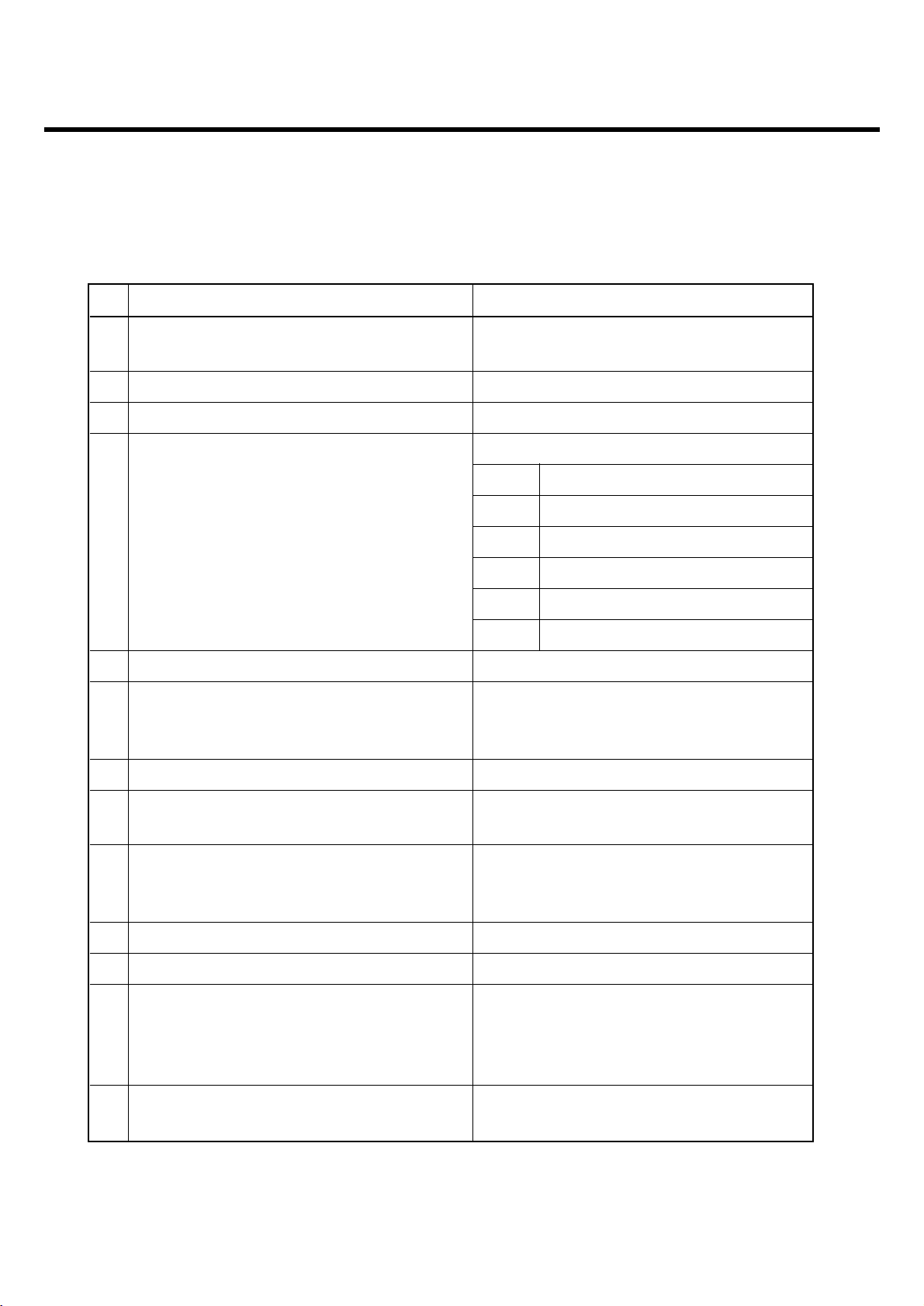
Item Specification
Shape GSM900/1800/1900 and WCDMA Communicator Handset
Size 108.9 X 53.9 X 17.2 mm
Weight 127 g (with 950mAh Battery)
Power 3.7V normal, 950 mAh Li-Polymer
Talk Time Over 170 min (TX = 12dBm,Low Power mode)
(with 950mAh) Over 180 min (TX Level = Max)
Standby Time Over 220 hours (DRX = 1.28)
(with 950mAh) Over 290 hours (Paging Period = 5)
Antenna Internal type and Antenna
LCD TFT LCD ( Main : 2.4’, 320 x 240, Sub :1.45” 160X64 )
LCD Backlight LED Back Light (Main, Sub)
Camera Dual Camera ; 2 Mega pixel (CMOS), VGA Camera (CMOS)
Vibrator Yes (Cylinder Type)
LED Indicator No
MIC Yes
Receiver Yes
Earphone Jack Yes
Connectivity Bluetooth, USB
Volume Key Push Type (+, -)
External Memory Micro-SD
I/O Connect 18 Pin

LGE Internal Use Only
Copyright © 2008 LG Electronics. Inc. All right reserved.
Only for training and service purposes
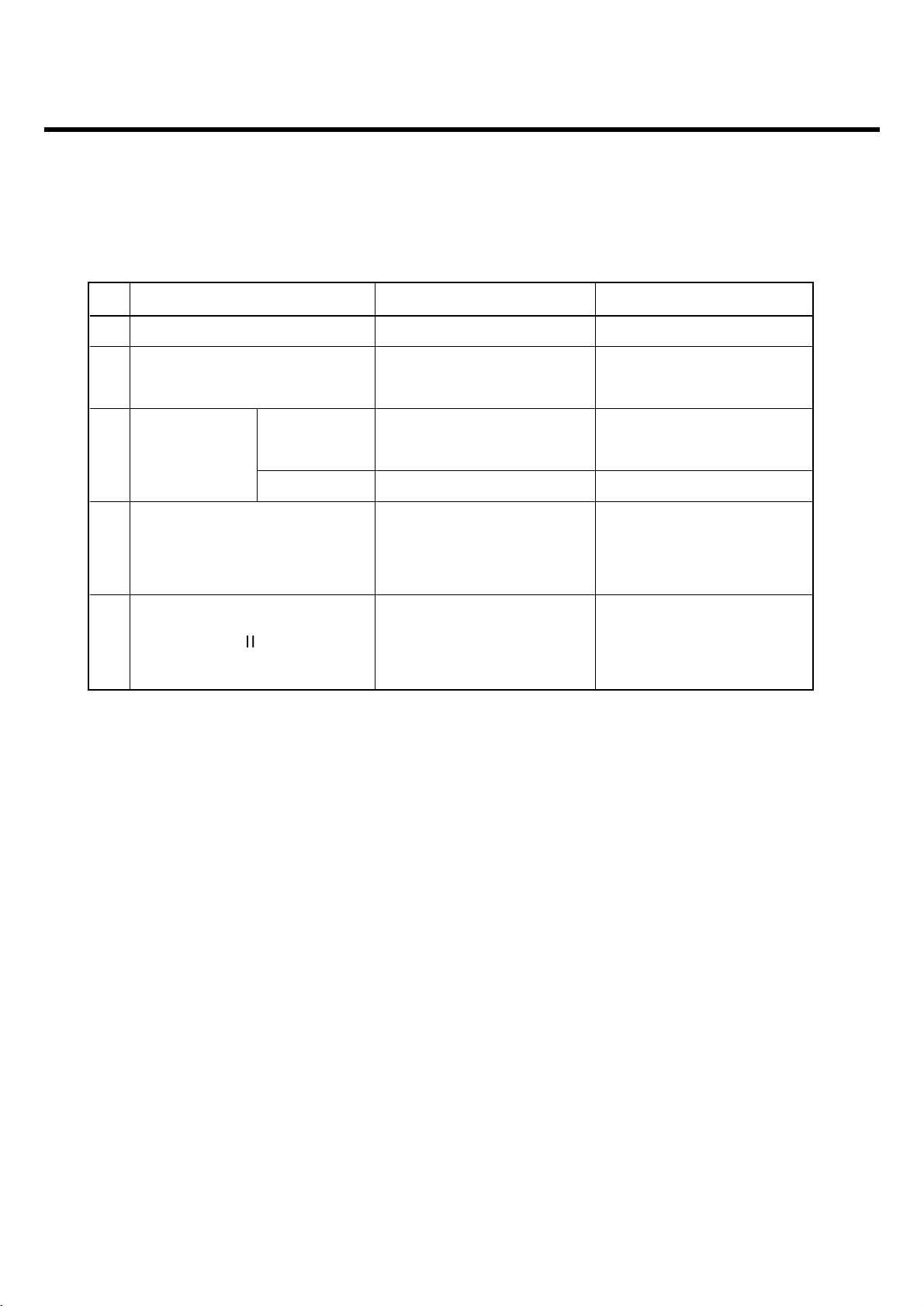
2.2 Usable environment
2.2.1 Environment
2.2.2 Environment (Accessory)
* CLA : 12~24V(DC).
2. PERFORMANCE
- 8 -
Item Specification
Voltage 3.7 V(Typ), [Shut Down : 3.22 V]
Operation Temp -20 ~ +60 °C
Storage Temp -20 ~ +70 °C
Humidity 85 % (Max)
Reference Spec. Min Typ. Max Unit
TA Power Available power 100 220 240 Vac
LGE Internal Use Only
Copyright © 2008 LG Electronics. Inc. All right reserved.
Only for training and service purposes
2. PERFORMANCE
- 9 -
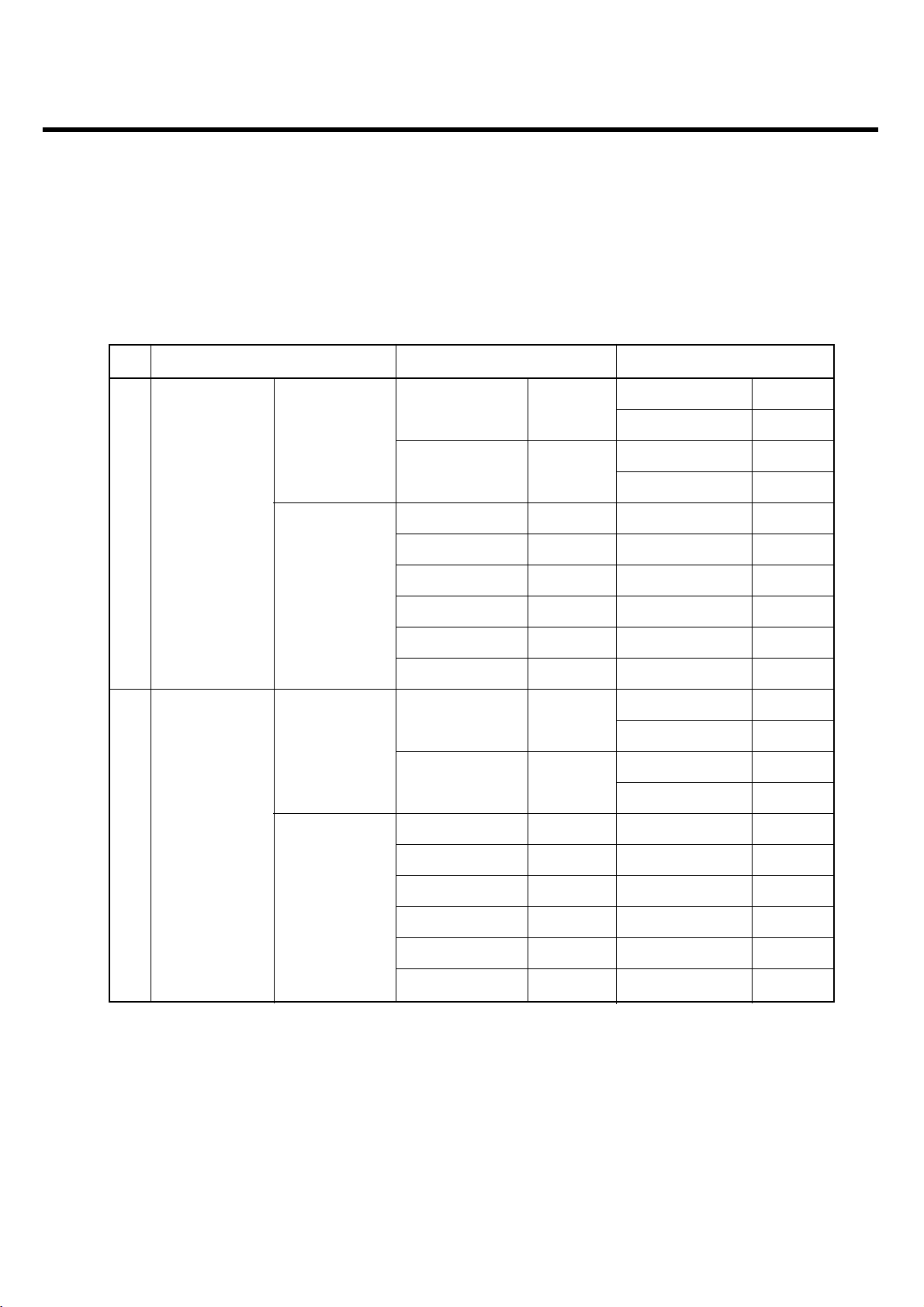
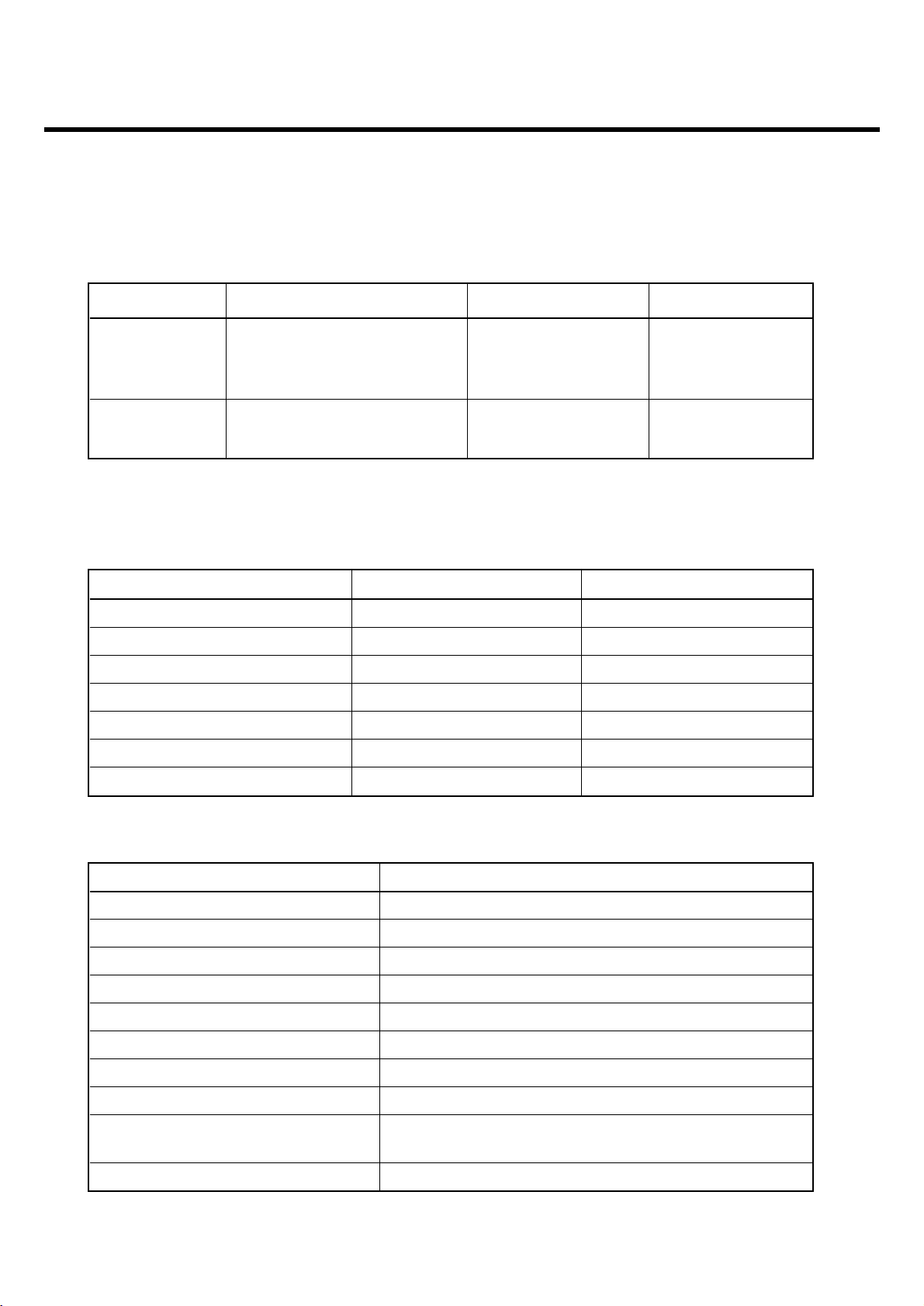
2.3 Radio Performance
2.3.1 Transmitter - GSM Mode
* In case of DCS : [A] -> 1710, [B] -> 1785* In case of PCS : [A] -> 1850, [B] -> 1910
No Item GSM DCS & PCS
1 Conducted MS allocated 100k~1GHz -39dBm 9k ~ 1GHz -39dBm
Spurious Channel 1G~[A]MHz -33dBm
Emission 1G~12.75GHz -33dBm [A]M~[B]MHz -39dBm
[B]M~12.75GHz -33dBm
Idle Mode 100k~880MHz -60dBm 100k~880MHz -60dBm
880M~915MHz -62dBm 880M~915MHz -62dBm
915M~1GHz -60dBm 915M~1GHz -60dBm
1G~[A]MHz -50dBm 1G~[A]MHz -50dBm
[A]M~[B]MHz -56dBm [A]M~[B]MHz -56dBm
[B]M~12.5GHz -50dBm [B]M~12.5GHz -50dBm
2 Radiated MS allocated 30M ~ 1GHz -36dBm 30M~1GHz 36dBm
Spurious Channel 1G~[A]MHz -30dBm
Emission 1G ~ 4GHz -30dBm [A]M~[B]MHz -36dBm
[B]M~4GHz -30dBm
Idle Mode 30M ~ 880MHz -57dBm 30M~880MHz -57dBm
880M ~ 915MHz -59dBm 880M~915MHz -59dBm
915M~1GHz -57dBm 915M~1GHz -57dBm
1G~[A]MHz -47dBm 1G~[A]MHz -47dBm
[A]M~[B]MHz -53dBm [A]M~[B]MHz -53dBm
[B]M~4GHz -47dBm [B]M~4GHz -47dBm
* In case of DCS : [A] -> 1710, [B] -> 1785* In case of PCS : [A] -> 1850, [B] -> 1910
LGE Internal Use Only
Copyright © 2008 LG Electronics. Inc. All right reserved.
Only for training and service purposes
2. PERFORMANCE
- 10 -
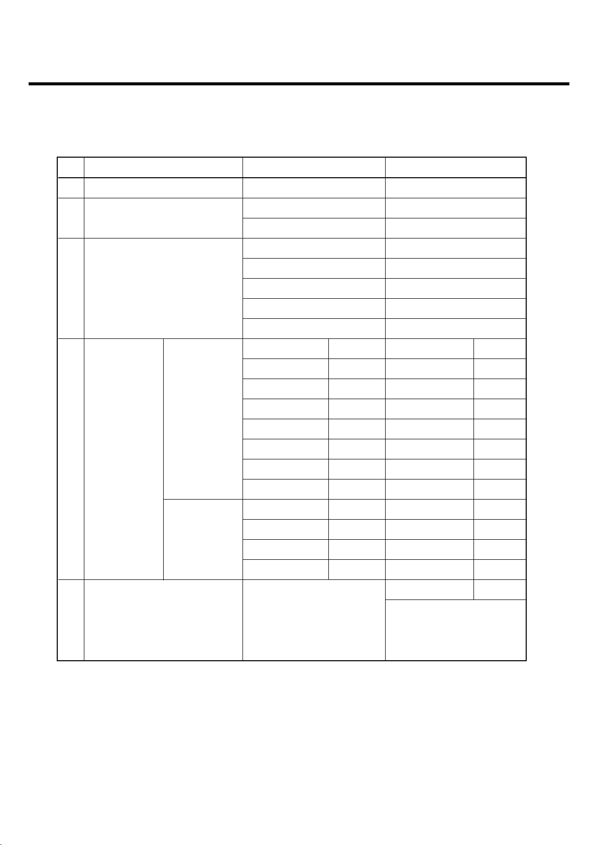
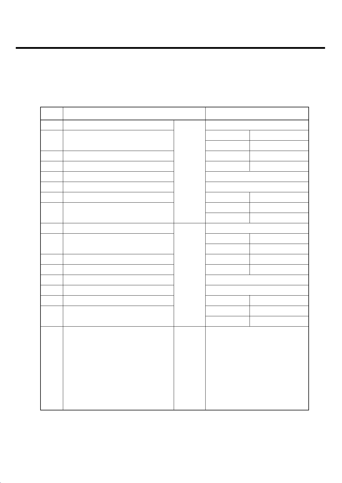
No Item GSM DCS & PCS
3 Frequency Error ± 0.1ppm ± 0.1ppm
4 Phase Error ± 5(RMS) ± 5(RMS)
± 20(PEAK) ± 20(PEAK)
5 Frequency Error 3dB below reference sensitivity 3dB below reference sensitivity
Under Multipath and RA250 : ± 200Hz RA250: ± 250Hz
Interference Condition HT100 : ± 100Hz HT100: ± 250Hz
TU50 : ± 100Hz TU50: ± 150Hz
TU3 : ± 150Hz TU1.5: ± 200Hz
6 Output RF Due to 0 ~ 100kHz +0.5dB 0 ~ 100kHz +0.5dB
Spectrum modulation 200kHz -30dB 200kHz -30dB
250kHz -33dB 250kHz -33dB
400kHz -60dB 400kHz -60dB
600 ~ 1800kHz -60dB 600 ~ 1800kHz -60dB
1800 ~ 3000kHz -63dB 1800 ~ 6000kHz -65dB
3000 ~ 6000kHz -65dB ≥ 6000kHz -73dB
≥ 6000kHz -71dB
Due to 400kHz -19dB 400kHz -22dB
Switching 600kHz -21dB 600kHz -24dB
transient 1200kHz -21dB 1200kHz -24dB
1800kHz -24dB 1800kHz -27dB
7 Intermodulation attenuation - Frequency offset 800kHz
Intermodulation product should
be Less than 55dB below the
level of Wanted signal
LGE Internal Use Only
Copyright © 2008 LG Electronics. Inc. All right reserved.
Only for training and service purposes
2. PERFORMANCE
- 11 -
No Item GSM DCS & PCS
8 Transmitter Output Power Level Power Toler. Level Power Toler.
533 ±3030 ±3
631 ±3128 ±3
729 ±3226 ±3
827 ±3324 ±3
925 ±3422 ±3
10 23 ±3 5 20 ±3
11 21 ±3 6 18 ±3
12 19 ±3 7 16 ±3
13 17 ±3 8 14 ±3
14 15 ±3 9 12 ±4
15 13 ±3 10 10 ±4
16 11 ±5 11 8 ±4
17 9 ±5 12 6 ±4
18 7 ±5 13 4 ±4
19 5 ±5 14 2 ±5
15 0 ±5
9 Burst timing Mask IN Mask IN
LGE Internal Use Only
Copyright © 2008 LG Electronics. Inc. All right reserved.
Only for training and service purposes
2. PERFORMANCE
- 12 -
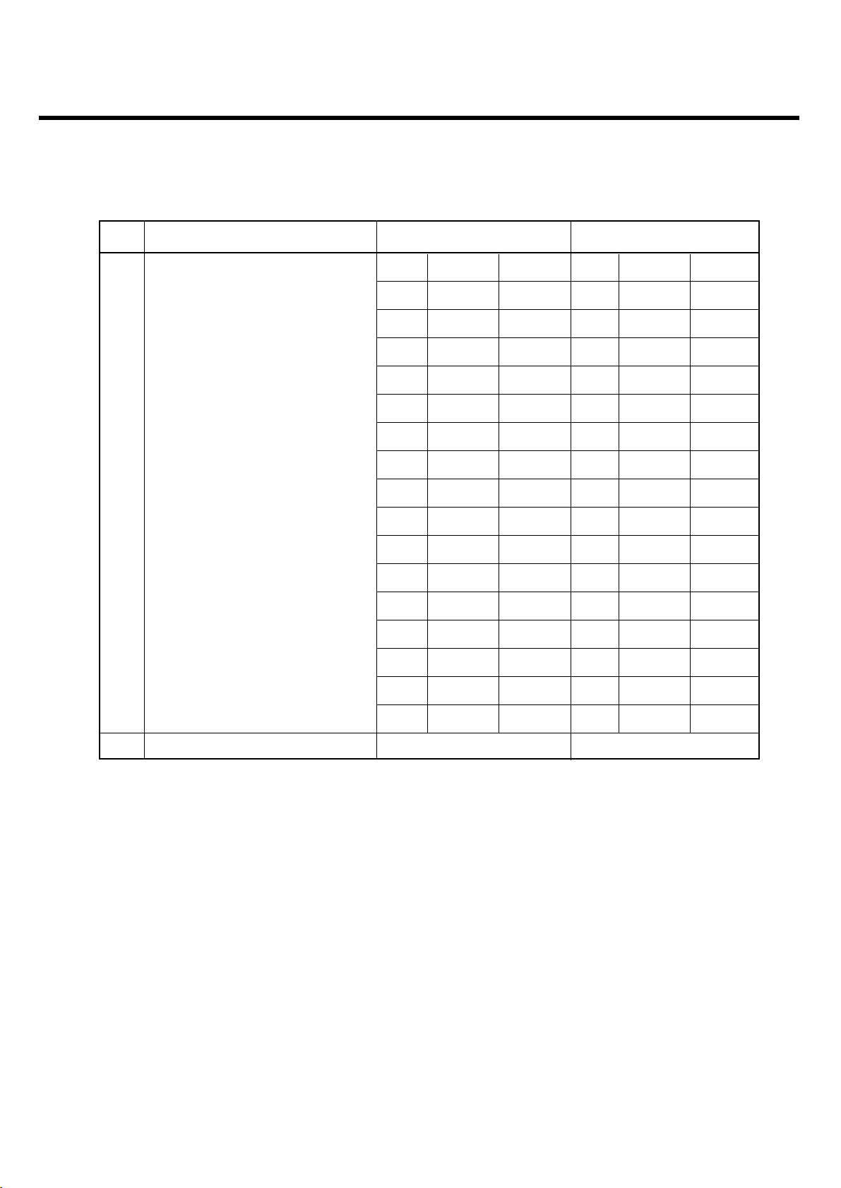
2.3.2 Transmitter - WCDMA Mode
No Item Specification
1 Maximum Output Power Class3: +24dBm(+1/-3dB)
Class 4 : +21dBm( ± 2dB)
2 Frequency Error ± 0.1ppm
3 Open Loop Power control in uplink ± 9dB@normal, ± 12dB@extreme
4 Inner Loop Power control in uplink Adjust output(TPC command)
cmd 1dB 2dB 3dB
+1 +0.5/1.5 +1/3 +1.5/4.5
0 -0.5/+0.5 -0.5/+0.5 -0.5/+0.5
-1 -0.5/-1.5 -1/-3 -1.5/-4.5
Group (10 equel command group)
+1 +8/+12 +16/+24
5 Out-band Blocking -50dBm(3.84MHz)
6 Out-of-synchronization handling of output power Qin/Qout : PCCH quality levels
Toff@DPCCH/Ior : -22 -> -28dB
Ton@DPCCH/Ior : -24 -> -18dB
7 Transmit OFF Power -56dBm(3.84MHz)
8 Transmit ON/OFF Time Mask ± 25us
PRACH,CPCH,uplinlk compressed mode
9 Change of TFC ± 25us
Power varies according to the data rate DTX :
DPCH off (minimize interference between UE)
10 Power setting in uplink compressed ± 3dB(after 14slots transmission gap)
11 Occupied Bandwidth(OBW) 5MHz(99%)
12 Spectrum emission Mask -35-15*(∆f-2.5)dBc@∆f=2.5~3.5MHz,30k
-35-1*(∆f-3.5)dBc@∆f=3.5~7.5MHz,1M -39-
10*(∆f-7.5)dBc@∆f=7.5~8.5MHz,1M
-49dBc@∆f=8.5~12.5MHz,1M
13 Adjacent Channel Leakage Ratio(ACLR) 33dB@5MHz, ACP>-50dBm
43dB@10MHz, ACP>-50dBm

LGE Internal Use Only
Copyright © 2008 LG Electronics. Inc. All right reserved.
Only for training and service purposes
2. PERFORMANCE
- 13 -
No Item Specification
14 Spurious Emissions (*: additional requirement) -36dBm@f=9~150KHz, 1K BW
-36dBm@f=50KHz~30MHz, 10K BW
-36dBm@f=30MHz~1000MHz, 100K BW
-30dBm@f=1~12.5GHz, 1M BW
(*)-41dBm@f=1893.5~1919.6MHz, 300K
(*)-67dBm@f=925~935MHz, 100K BW
(*)-79dBm@f=935~960MHz, 100K BW
(*)-71dBm@f=1805~1880MHz, 100K BW
15 Transmit Intermodulation -31dBc@5MHz,Interferer -40dBc
-41dBc@10MHz, Interferer -40dBc
16 Error Vector Magnitude (EVM) 17.5%(>-20dBm)
(@12.2K, 1DPDCH+1DPCCH)
17 Transmit OFF Power -15dB@SF=4.768Kbps, Multi-code
transmission
- 14 -
2. PERFORMANCE
LGE Internal Use Only
Copyright © 2008 LG Electronics. Inc. All right reserved.
Only for training and service purposes
2.3.3 Receiver - GSM Mode
No Item GSM DCS & PCS
1 Sensitivity (TCH/FS Class II) -105dBm -105dBm
2 Co-Channel Rejection (TCH/FS C/Ic=7dB Storage -30 ~ +85
Class II, RBER, TU high/FH)
3 Adjacent 200kHz C/Ia1=-12dB C/Ia1=-12dB
Channel
Rejection 400kHz C/Ia2=-44dB C/Ia2=-44dB
4 Intermodulation Rejection Wanted Signal :-98dBm Wanted Signal :-96dBm
1st interferer :-44dBm 1st interferer :-44dBm
2nd interferer :-45dBm 2nd interferer :-44dBm
5 Blocking Response Wanted Signal :-101dBm Wanted Signal :-101dBm
(TCH/FS Class , RBER) Unwanted : Depend on Unwanted : Depend on
Frequency Frequency

- 15 -
2. PERFORMANCE
LGE Internal Use Only
Copyright © 2008 LG Electronics. Inc. All right reserved.
Only for training and service purposes
2.3.4 Receiver - WCDMA Mode
No Item Specification
1 Reference Sensitivity Level -106.7 dBm(3.84 MHz)
2 Maximum Input Level -25dBm(3.84MHz)
-44dBm/3.84MHz(DPCH_Ec)
UE@+20dBm output power(Class3)
3 Adjacent Channel Selectivity (ACS) 33dB
UE@+20dBm output power(Class3)
4In-band Blocking -56dBm/3.84MHz@10MHz
UE@+20dBm output power(Class3)
-44dBm/3.84MHz@15MHz
UE@+20dBm output power(Class3)
5 Out-band Blocking -44dBm/3.84MHz@f=2050~2095 and
2185~2230MHz
UE@+20dBm output power(Class3)
-30dBm/3.84MHz@f=2025~2050 and
2230~2255MHz
UE@+20dBm output power(Class3)
-15dBm/3.84MHz@f=1~2025 and
2255~12500MHz
UE@+20dBm output power(Class3)
6 Spurious Response -44dBm CW
UE@+20dBm output power(Class3)
7 Intermodulation Characteristic -46dBm CW@10MHz
-46dBm/3.84MHz@20MHz
UE@+20dBm output power(Class3)
8 Spurious Emissions -57dBm@f=9KHz~1GHz, 100K BW
-47dBm@f=1~12.5GHz, 1M BW
-60dBm@f=1850 MHz ≤ f ≤ 1910 MHz,
3.84M BW
-60dBm@f=824 MHz ≤ f ≤ 849 MHz, 3.84M BW
- 16 -
2. PERFORMANCE
LGE Internal Use Only
Copyright © 2008 LG Electronics. Inc. All right reserved.
Only for training and service purposes
2.4 Current Consumption
(Stand by and Voice Call Test Condition : LCD backlight Off)
(VT Test Condition : Speaker off, LCD backlight On,0dBm Tx power)
2.5 RSSI BAR
2.6 Battery BAR
Stand by(BT Off condition) Voice Call VT
WCDMA Under 4.32 mA Under 335 mA Under 569mA
(DRX=1.28) (Tx=10dBm) (Tx=10dBm
-Low power) -Low power)
GSM Under 4.32 mA Under 380 mA
(Paging=5period) (Tx=Max power)
Level Change CDMA GSM
7 → 6 -86 ± 2dBm -82 ± 2dBm
6 → 5 -90 ± 2dBm -86 ± 2dBm
5 → 4 -94 ± 2dBm -90 ± 2dBm
4 → 3 -98 ± 2dBm -94 ± 2dBm
3 → 2 -102 ± 2dBm -98 ± 2dBm
2 → 1 -106 ± 2dBm -102 ± 2dBm
1 → 0 -110 ± 2dBm -106 ± 2dBm
Indication Standby
Bar 7 3.96 ± 0.05V
Bar 7 → 6 3.95 ± 0.05V
Bar 6 → 5 3.86 ± 0.05V
Bar 5 → 4 3.78 ± 0.05V
Bar 4 → 3 3.74 ± 0.05V
Bar 3 → 2 3.69 ± 0.05V
Bar 2 → 1 3.63 ± 0.05V
Bar 1 → Empty 3.50 ± 0.05V
Low Voltage, 3.63,3.50 ± 0.05V (Stand-by) / 3.63, 3.50 ± 0.05V (Talk)
Warning message + tone Bar 2 → 1 / Bar 1 → Empty
Power Off 3.20 ± 0.05V
- 17 -
2. PERFORMANCE
LGE Internal Use Only
Copyright © 2008 LG Electronics. Inc. All right reserved.
Only for training and service purposes
2.7 Sound Pressure Level
No Test Item Specification
1 Sending Loudness Rating (SLR) 8 ± 3 dB
2 Receiving Loudness Rating (RLR) Nor -4 ± 3 dB
Max -15 ± 3 dB
3 Side Tone Masking Rating (STMR) Min 17 dB
4 Echo Loss (EL) Min 40 dB
5 Sending Distortion (SD) Refer to Table 30.3
6 Receiving Distortion (RD) Refer to Table 30.4
7 Idle Noise-Sending (INS) Max -64 dBm0p
8 Idle Noise-Receiving (INR) Nor Under -47 dBPA
Max Under -36 dBPA
9 Sending Loudness Rating (SLR) 8 ± 3 dB
10 Receiving Loudness Rating (RLR) Nor -1 ± 3 dB
Max -12 ± 3 dB
11 Side Tone Masking Rating (STMR) Min 25 dB
12 Echo Loss (EL) Min 40 dB
13 Sending Distortion (SD) Refer to Table 30.3
14 Receiving Distortion (RD) Refer to Table 30.4
15 Idle Noise-Sending (INS) Max -55 dBm0p
16 Idle Noise-Receiving (INR) 16 Nor Under -45 dBPA
Max Under -40 dBPA
17 TDMA Noise Max -62 dBm
-. GSM : Power Level : 5
DCS/PCS : Power Level : 0
(Cell Power : -90 ~ -105 dBm)
-. Acoustic (Max Vol.)
MS/Headset SLR : 8 ± 3dB
MS/Headset RLR : -15 ± 3dB / -12dB
(SLR/RLR : Mid-value setting)
MS
Headset
MS and
Headset

- 18 -
2. PERFORMANCE
LGE Internal Use Only
Copyright © 2008 LG Electronics. Inc. All right reserved.
Only for training and service purposes
2.8 Charging
• Charging Method : CC & CV (Constant Current & Constant Voltage)
• Maximum Charging Voltage : 4.2 V
• Maximum Charging Current : 650mA
• Normal Battery Capacity : 950 mAh
• Charger Voltage : 4.8V
• Charging Time : Max 3 h (Except time trickle charging)
• Full charging indication current (charging icon stop current) : 60mA
• Low battery POP UP : 3.48V
• Low battery alarm interval : Idle - 3 min, Dedicated - 1min
• Cut-off voltage : 3.22V
- 19 -
3. TECHNICAL BRIEF
3. TECHNICAL BRIEF
LGE Internal Use Only
Copyright © 2008 LG Electronics. Inc. All right reserved.
Only for training and service purposes
3.1 GENERAL DESCRIPTION
The KT615 supports UMTS-2100, GSM-900, GSM-1800, and GSM-1900 based
GSM/GPRS/EDGE/UMTS. All receivers and the UMTS transmitter use the radioOne1Zero-IF
architecture to eliminate intermediate frequencies, directly converting signals between RF and
baseband. The quad-band GSM transmitters use a baseband-to-IF upconversion followed by an offset
phase-locked loop that translates the GMSK-modulated or 8-PSK-modulated signal to RF.
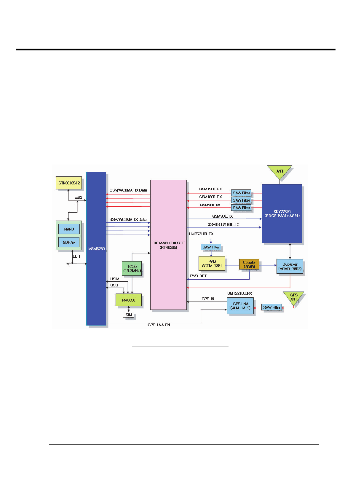
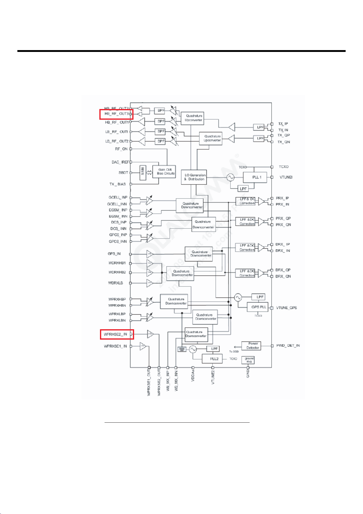
A generic, high-level functional block diagram of KT615 is shown in Figure 3-1. One antenna collects
base station forward link signals and radiates handset reverse link signals. The antenna connects with
receive and transmit paths through a SKY77519(EDGE PAM+ASM). The UMTS receive paths each
include an LNA, an RF band-pass filter, and a downconverter that translate the signal directly from RFto-baseband using radioOne ZIF techniques.
The RFIC’s Rx analog baseband outputs, for the receive chains, connect to the MSM IC. The UMTS
and GSM Rx baseband outputs share the same inputs to the MSM IC.
[Fig. 3.1] Block diagram of RF part
1
QUALCOMM’s branded chipset that implements a Zero-IF radio architecture.

LGE Internal Use Only
Copyright © 2008 LG Electronics. Inc. All right reserved.
Only for training and service purposes
3. TECHNICAL BRIEF
- 20 -
For the transmit chains, the RTR6285 IC directly translates the Tx baseband signals (from the MSM
device) to an RF signal using an internal LO generated by integrated on-chip PLL and VCO. The
RTR6285 IC outputs deliver fairly high-level RF signals that are first filtered by Tx SAWs and then
amplified by their respective UMTS PAs.
In the GSM receive path, the received RF signals are applied through their bandpass filters and downconverted directly to baseband in the RTR6285 transceiver IC.
These baseband outputs are shared with the UMTS receiver and routed to the MSM IC for further
signal processing.
The GSM/EDGE transmit path employs one stage of up-conversion and, in order to improve efficiency,
is divided into phase and amplitude components to produce an open-loop Polar topology:
1. The on-chip quadrature up-converter translates the GMSK-modulated signal or 8- PSK modulated
signal, to a constant envelope phase signal at RF;
2. The amplitude-modulated (AM) component is applied to the ramping control pin of Polar power
amplifier from a DAC within the MSM
KT615 power supply voltages are managed and regulated by the PM6658 Power Management IC.
This versatile device integrates all wireless handset power management, general housekeeping, and
user interface support functions into a single mixed signal IC. It monitors and controls the external
power source and coordinates battery recharging while maintaining the handset supply voltages using
low dropout, programmable regulators.
The device’s general housekeeping functions include an ADC and analog multiplexer circuit for
monitoring on-chip voltage sources, charging status, and current flow, as well as user-defined off-chip
variables such as temperature, RF output power, and battery ID. Various oscillator, clock, and counter
circuits support IC and higher-level handset functions. Key parameters such as under-voltage lockout
and crystal oscillator signal presence are monitored to protect against detrimental conditions.
LGE Internal Use Only
Copyright © 2008 LG Electronics. Inc. All right reserved.
Only for training and service purposes
3. TECHNICAL BRIEF
- 21 -
3.2 GSM MODE
3.2.1 GSM RECEIVER
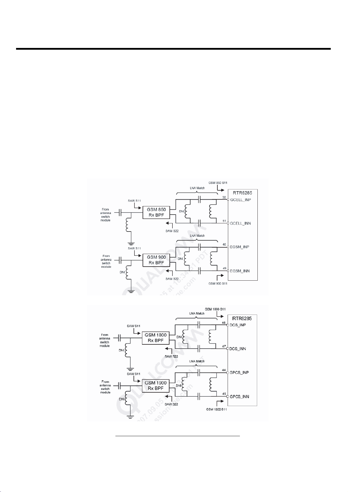
The GSM-900, GSM-1800, and GSM-1900 receiver inputs of RTR6285 are connected directly to the
transceiver front-end circuits(filters and antenna switch module). GSM-900, GSM-1800, and GSM1900 receiver inputs use differential configurations to improve common-mode rejection and secondorder non-linearity performance as shown in Figure 3-2. The balance between the complementary
signals is critical and must be maintained from the RF filter outputs all the way into the IC pins
[Figure 3-2] GSM Receiver Inputs Topologies

LGE Internal Use Only
Copyright © 2008 LG Electronics. Inc. All right reserved.
Only for training and service purposes
3. TECHNICAL BRIEF
- 22 -
Since GSM-900, GSM-1800, and GSM-1900 signals are time-division duplex (the handset can only
receive or transmit at one time), switches are used to separate Rx and Tx signals in place of frequency
duplexers - this is accomplished in the switch module. The GSM-900, GSM-1800, and GSM-1900
receive signals are routed to the RTR6285 through band selection filters and matching networks that
transform singleended 50-Ω sources to differential impedances optimized for gain and noise figure.
The RTR input uses a differential configuration to improve second-order intermodulation and common
mode rejection performance. The RTR6285 input stages include MSM-controlled gain adjustments that
maximize receiver dynamic range.
The amplifier outputs drive the RF ports of the quadrature RF-to-baseband downconverters. The
downconverted baseband outputs are multiplexed and routed to lowpass filters (one I and one Q)
having passband and stopband characteristics suitable for GMSK or 8-PSK processing. These filter
circuits include DC offset corrections. The filter outputs are buffered and passed on to the MSM6280 IC
for further processing as shown in Figure 3-4.
LGE Internal Use Only
Copyright © 2008 LG Electronics. Inc. All right reserved.
Only for training and service purposes
3. TECHNICAL BRIEF
- 23 -
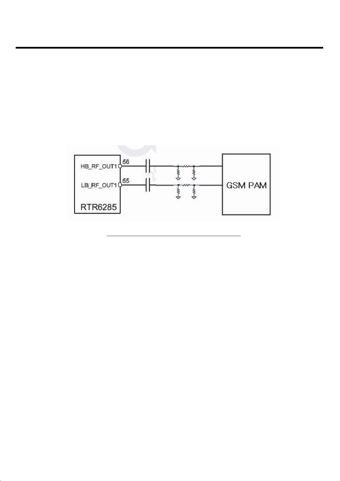
3.2.2 GSM TRANSMITTER
The RTR6285 transmitter outputs(HB_RF_OUT1 and LB_RF_OUT1) include on-chip output matching
inductors. 50ohm output impedance is achieved by adding a series capacitor at the output pins. The
capacitor value may be optimized for specific applications and PCB characteristics based on pass-band
symmetry about the band center frequency as shown in Figure 3-3.
The RTR6285 IC is able to support GSM 900 and GSM 1800/1900 mode transmitting.
This design guideline shows a tri-band GSM application. Both high-band and low band outputs are
followed by resistive pads to ensure that the load presented to the outputs remains close to 50ohm.
[Figure 3-3] GSM Transmitter Outputs Topologies
LGE Internal Use Only
Copyright © 2008 LG Electronics. Inc. All right reserved.
Only for training and service purposes
3. TECHNICAL BRIEF
- 24 -
3.3 UMTS MODE
3.3.1 UMTS RECEIVER
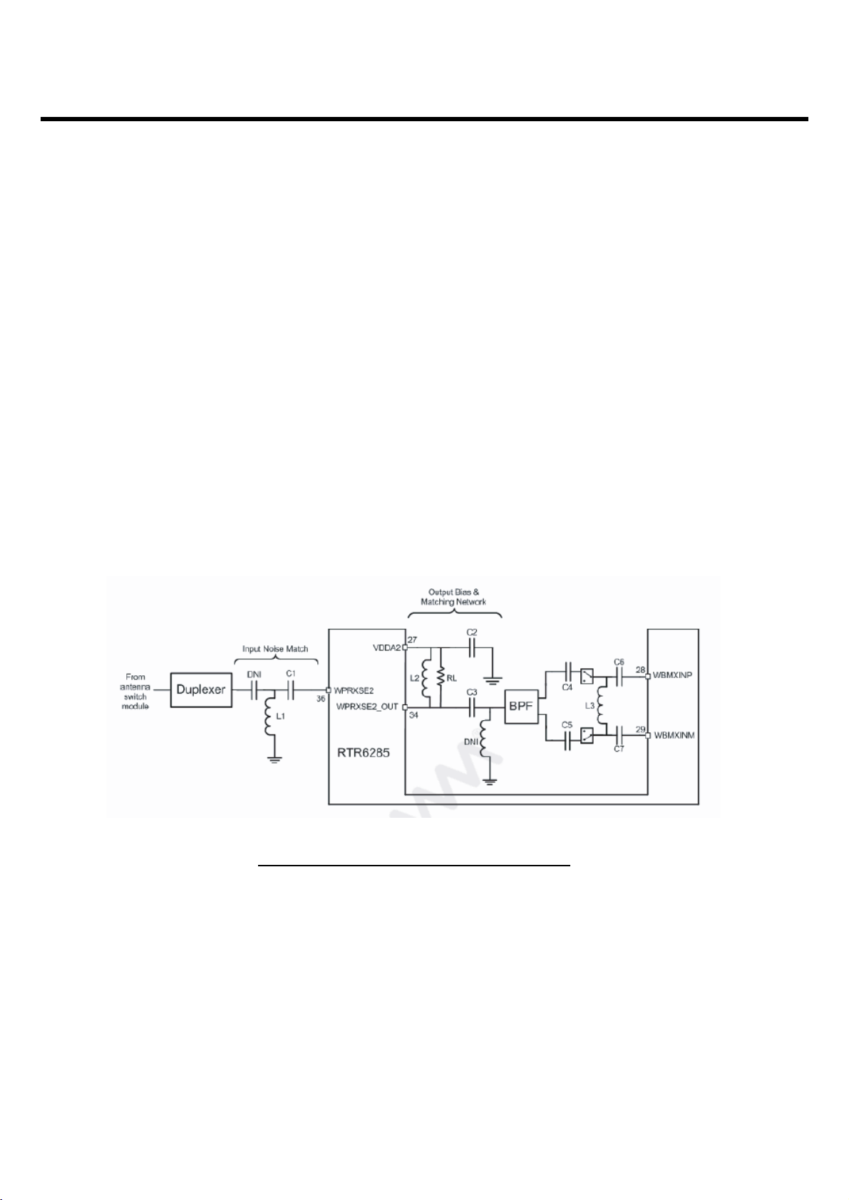
The UMTS duplexer receiver output is routed to LNA circuits within the RTR6285 device as shown in
Figure 3-4. The UMTS Rx input is provided with an on-chip LNA that amplifies the signal before a
second stage filter that provides differential downconverter as shown in Figure 3-5. This second stage
input is configured differentially to optimize second-order intermodulation and common mode rejection
performance. The gain of the UMTS frontend amplifier and the UMTS second stage differential amplifier
are adjustable, under MSM control, to extend the dynamic range of the receivers. The second stage
UMTS Rx amplifiers drive the RF ports of the quadrature RF-to-baseband downconverters. The
downconverted UMTS Rx baseband outputs are routed to lowpass filters having passband and
stopband characteristics suitable for UMTS Rx processing. These filter circuits allow DC offset
corrections, and their differential outputs are buffered to interface shared with GSM Rx to the MSM IC.
The UMTS baseband outputs are turned off when the RTR6285 is downconverting GSM signals and on
when the UMTS is operating.
[Figure 3-4] UMTS Receiver Inputs Topologies

LGE Internal Use Only
Copyright © 2008 LG Electronics. Inc. All right reserved.
Only for training and service purposes
3. TECHNICAL BRIEF
- 25 -
3.3.2 UMTS TRANSMITTER
The UMTS Tx path begins with differential baseband signals (I and Q) from the MSM device.
These analog input signals are amplified, filtered, and applied to the quadrature upconverter mixers.
The up-converter output is amplified by multiple variable gain stages that provide transmit AGC control.
The AGC output is filtered and applied to the driver amplifier; this output stage includes an integrated
matching inductor that simplifies the external matching network to a single series capacitor to achieve
the desired 50-Ω interface.
The RTR6285 UMTS output is routed to its power amplifier through a bandpass filter, and delivers fairly
high-level signals that are filtered and applied to the PA. Transmit power is delivered from the duplexer
to the antenna through the switch module.
The transceiver LO synthesizer is contained within the RTR6285 IC with the exception of the off-chip
loop filter components and the VC-TCXO. This provides a simplified design for multimode applications.
The PLL circuits include a reference divider, phase detector, charge pump, feedback divider, and digital
logic generator.
UMTS Tx. Using only PLL1, the LO generation and distribution circuits create the necessary LO signals
for nine different frequency converters. The UMTS transmitter also employs the ZIF architecture to
translate the signal directly from baseband to RF.
This requires FLO to equal FRF, and the RTR6285 IC design achieves this without allowing FVCO to
equal FRF.
The RTR6285 IC is able to support UMTS 2100/1900/1800/1700 and 850 mode transmitting. This
design guideline shows only UMTS 2100 applications.
- 26 -
3. TECHNICAL BRIEF
LGE Internal Use Only
Copyright © 2008 LG Electronics. Inc. All right reserved.
Only for training and service purposes
WCDMA_2100_TX
WCDMA_2100_RX
[Figure 3.5] RTR6285 IC Functional Block Diagram

- 27 -
3. TECHNICAL BRIEF
3.4 GPS MODE
3.4.1 GPS RECEIVER
The GPS receicer input employs a single-ended connection realized by this pin. The GPS input is
routed from the GPS antenna switch, through a bandpass filter and then an impedance transformer
circuit that optimally matches the impedance looking into the GPS LNA. The impedance transformer
circuit topology is shown in Figure 3-6.
LGE Internal Use Only
Copyright © 2008 LG Electronics. Inc. All right reserved.
Only for training and service purposes
[Figure 3.6] GPS Input Network Topology

LGE Internal Use Only
Copyright © 2008 LG Electronics. Inc. All right reserved.
Only for training and service purposes
3. TECHNICAL BRIEF
- 28 -
3.5 LO GENERATION and DISTRIBUTION CIRCUIT
The integrated LO generation and distribution circuits are driven by internal VCOs to support various
modes to yield highly flexible quadrature LO outputs that drive all GSM/EDGE, UMTS band and GPS
upconverters and downconverters; with the help of these LO generation and distribution circuits, true
zero-IF architecture is employed in all GSM and UMTS band receivers and transmitters to translate the
signal directly from RF-to-baseband and from baseband-to-RF. Two fully functional fraction-N
synthesizers, including VCOs and loop filters, are integrated within the RTR6285 IC. In addition, the
RTR6285 has a third synthesizer used for GPS operation. The first synthesizer (PLL1) in the RTR6285
creates the transceiver Los that support the UMTS transmitter, and all four GSM band receivers and
transmitters including:
GSM850, GSM900, GSM1800, and GSM1900. The second synthesizer (PLL2) in the RTR6285 IC
provides the LO for the UMTS primary receiver. For the RTR6285 IC only, the second synthesizer also
provides the LO for the secondary UMTS receiver.
The third synthesizer (PLL3), only in the RTR6285 IC, provides the LO for the GPS receiver. An
external TCXO input signal is required to provide the synthesizer frequency reference to which the PLL
is phase and frequency locked. The RTR6285 ICs integrate most of the PLL loop filter components onchip except for three off-chip loop filter-series capacitors, which significantly reduces off-chip
component requirement. With the integrated fractional-N PLL synthesizers, the RTR6285 ICs have the
advantage of more flexible loop bandwidth control, fast lock time, and lowintegrated phase error.

LGE Internal Use Only
Copyright © 2008 LG Electronics. Inc. All right reserved.
Only for training and service purposes
3. TECHNICAL BRIEF
- 29 -
3.6 OFF-CHIP RF COMPONENTS
3.6.1 ALM-1412(U603:GPS LNA)
The ALM-1412 is an LNA module, with integrated filter, designed for GPS band applications at
1.575GHz. The LNA uses AVAGO Technologies’ proprietary GaAs Enhancement-mode pHEMT
process to achieve high gain with very low noise figure and high linearity Noise figure distribution is very
tightly controlled. A CMOScompatible shutdown pin is included either for turning the LNA on/off, or for
current adjustment. The integrated filter utilizes an Avago Technologies’ leading edge FBAR filter for
exceptional rejection at Cell/PCS Band frequencies. The ALM-1412 is useable down to 1V operation. It
achieves low noise figure, high gain and linearity even at 1V, making it suitable for use in critical lowpower GPS applications or during low-battery situations.
3.6.2 SKY77519(U601:GSM FEM)
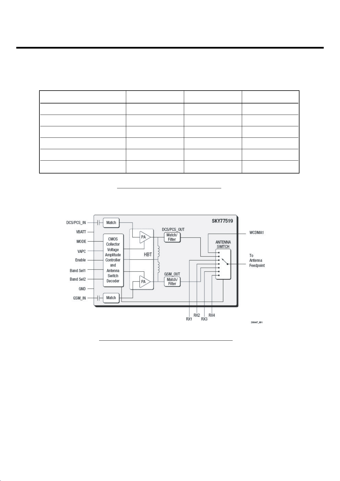
RF Front end consists of antenna, antenna switch module (SKY77519) which includes EDGE PAM.
The antenna switch module allows multiple operating bands and modes to share the same antenna. In
KT615, a common antenna connects to one of six paths: 1) UMTS-2100 Rx/Tx, 2) GSM-900 Rx, 3)
GSM-900 Tx, 4) GSM- 1800 Rx, and 5) GSM-1800, GSM-1900 Tx(High Band Tx’s share the same
path), 6) GSM-1900 Rx. UMTS operation requires simultaneous reception and transmission, so the
UMTS Rx/Tx connection is routed to a duplexer that separates receive and transmit signals. GSM-900,
GSM-1800, and GSM-1900 operation is time division duplexed, so only the receiver or transmitter is
active at any time and a frequency duplexer is not required. The active connection is MSM-selected by
three control lines (GPIO[9], GPIO[10] and GPIO[11]). These GPIOs are programmed to be ANT_SEL0
, ANT_SEL1 and ANT_SEL2 respectively.
LGE Internal Use Only
Copyright © 2008 LG Electronics. Inc. All right reserved.
Only for training and service purposes
3. TECHNICAL BRIEF
- 30 -
TXEN BS1 BS2
GSM 900 TX LOW LOW HIGH
GSM 1800/GSM 1900 TX LOW HIGH HIGH
GSM 900 RX HIGH HIGH LOW
GSM 1800 RX HIGH HIGH HIGH
GSM 1900 RX HIGH LOW HIGH
WCDMA LOW HIGH LOW
Table 1. Antenna Switch Module Logic
[Figure 3.5] SKY77519 Functional Block Diagram.
LGE Internal Use Only
Copyright © 2008 LG Electronics. Inc. All right reserved.
Only for training and service purposes
3. TECHNICAL BRIEF
- 31 -
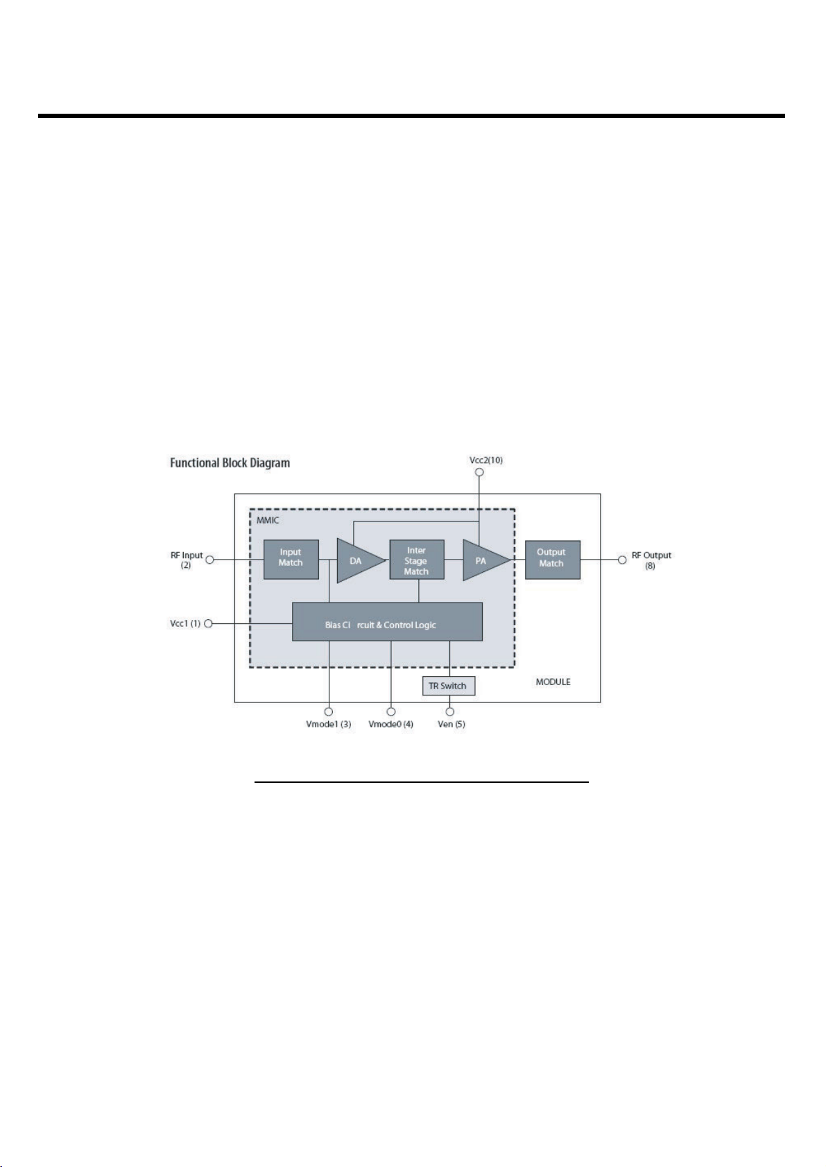
3.6.3 W-CDMA POWER AMPLIFIER (U604: ACPM-7381)
The ACPM-7381, a Wide-band Code Division Multiple Access(WCDMA) Power Amplifier(PA), is a fully
matched 10-pin surface mount module developed for WCDMA handset applications. This power
amplifier module is developed to cover 1920- 1980MHz bandwidth. The ACPM-7381 meets the
stringent WCDMA linearity requirements for output power of up to 28dBm. The ACPM-7381 is also
developed to meet HSDPA specs.
The ACPM-7381 is designed to enhance the efficiency at low and medium output power range by using
3-mode control scheme with 2 mode control pins. This provides extended talk time. The ACPM-7381 is
self contained, incorporating 50ohm input and output matching networks.
3.6.4 W-CDMA DUPLXER (FL605: ACMD-7602)
The ACMD-7602 is a miniature duplexer designed for use in UMTS Band I handsets and enhances the
sensitivity and dynamic range of WCDMA receivers by providing more than 53dB attenuation of the
transmitted signal at the receiver input and more than 43dB rejection of transmit-generated noise in the
receiver band. The ACMD-7602 is designed with FBAR technology, which makes possible ultra-small,
high-Q filters at a fraction of their usual size. The excellent power handling capability of the FBAR bulkmode resonators supports the high output power levels needed in handsets while adding virtually no
distortion.
[Figure 3.6] ACPM-7381 Functional Block Diagram.
 Loading...