

LG KG376 Service Manual
Date: September, 2009 / Issue 1.0
Service Manual
Model : KG376
Service Manual
KG376
Internal Use Only

- 1 -
LGE Internal Use Only
Copyright © 2007 LG Electronics. Inc. All right reserved.
Only for training and service purposes
The information in this manual is subject to change without notice and should not be construed as
a commitment by LGE Inc. Furthermore, LGE Inc. reserves the right, without notice, to make
changes to equipment design as advances in engineering and manufacturing methods warrant.
This manual provides the information necessary to install, program, operate and maintain the KG376.
REVISED HISTORY
Editor Date Issue Contents of Changes S/W Version

- 2 -
LGE Internal Use Only
Copyright © 2007 LG Electronics. Inc. All right reserved.
Only for training and service purposes

- 3 -
Table Of Contents
1. INTRODUCTION ...............................5
1.1 Purpose .................................................. 5
1.2 Regulatory Information............................ 5
1.3 ABBREVIATION ......................................7
2. PERFORMANCE...............................9
2.1 Product Name ..........................................9
2.2 Supporting Standard................................9
2.3 Main Parts: GSM Solution........................9
2.4 H/W Features.........................................10
3. TECHNICAL BRIEF ........................14
3.1 Digital Main Processor(PMB7880).........14
3.2 Power Amplifier Module (SKY77318) ....22
3.3 26 MHz Clock (DCXO)...........................24
3.4 RTC(32.768KHz Crystal) .......................25
3.5 LCD Interface(3-wire SPI interface) .......26
3.6 SIM Card Interface.................................28
3.7 KEYPAD Interface .................................29
3.8 Battery Charging Block Interface ...........30
3.9 RF Interface ...........................................31
3.10 Audio Interface.....................................33
3.11 Key LED Interface................................37
3.12 Vibrator Interface .................................38
3.13 Memory Interface .................................39
3.14 Power Block Interface ..........................40
3.15 MG377a, MG377b, KG376 Function
difference .............................................42
3.16 BOM difference ....................................43
4. TROUBLE SHOOTING ...................44
4.1 Trouble Test Set-up ...............................44
4.2 Power On Trouble..................................45
4.3 Charging Trouble ...................................47
4.4 Vibrator Trouble .....................................49
4.5 SIM Card Trouble...................................51
4.6 KEY backlight Trouble ...........................53
4.7 RTC Trouble ..........................................54
4.8 LCD Trouble...........................................55
4.9 Speaker Trouble ....................................57
4.10 Receiver Trouble..................................59
4.11 Headphone Trouble .............................60
4.12 Microphone Trouble .............................62
4.13 RF Components...................................63
4.14 RX Receiver Part .................................64
4.14 RX Receiver Part .................................66
4.15 TX Transmitter Part..............................67
5. DOWNLOAD.......................................71
5.1 Download Setup.....................................71
5.2 Download Process .................................72
6. BLOCK DIAGRAM ..........................77
7. CIRCUIT DIAGRAM ........................79
8. BGA IC Pin Check .............................83
9. PCB LAYOUT..................................85
10. Calibration ....................................87
10.1 Calibration Steps..................................87
11. Stand-alone Test ..........................92
11.1 Test Program Setting ...........................92
11.2 Tx Test .................................................94
11.3 Rx Test.................................................95
12. EXPLODED VIEW &
REPLACEMENT PART LIST ....... 97
12.1 Exploded View .................................... 97
12.2 Replacement Parts ..............................99
12.3 Accessory ......................................... 111
Table Of Contents
LGE Internal Use Only
Copyright © 2007 LG Electronics. Inc. All right reserved.
Only for training and service purposes

- 4 -
LGE Internal Use Only
Copyright © 2007 LG Electronics. Inc. All right reserved.
Only for training and service purposes

- 5 -
1. INTRODUCTION
1.1 Purpose
This manual provides the information necessary to repair, calibration, description and download the
features of the KG376
1.2 Regulatory Information
A. Security
Toll fraud, the unauthorized use of telecommunications system by an unauthorized part (for example,
persons other than your company’s employees, agents, subcontractors, or person working on your
company’s behalf) can result in substantial additional charges you’re your telecommunications
services. System users are responsible for the security of own system. There are may be risks of toll
fraud associated with your telecommunications system. System users are responsible for
programming and configuring the equipment to prevent unauthorized use. LGE does not warrant that
this product is immune from the above case but will prevent unauthorized use of common-carrier
telecommunication service of facilities accessed through or connected to it. LGE will not be
responsible for any charges that result from such unauthorized use.
B. Incidence of Harm
If a telephone company determines that the equipment provided to customer is faulty and possibly
causing harm or interruption in service to the telephone network, it should disconnect telephone
service until repair can be done. A telephone company may temporarily disconnect service as long as
repair is not done.
C. Changes in Service
A local telephone company may make changes in its communications facilities or procedure. If these
changes could reasonably be expected to affect the use of the KG376 or compatibility with the
network, the telephone company is required to give advanced written notice to the user, allowing the
user to take appropriate steps to maintain telephone service.
D. Maintenance Limitations
Maintenance limitations on the KG376 must be performed only by the LGE or its authorized agent.
The user may not make any changes and/or repairs expect as specifically noted in this manual.
Therefore, note that unauthorized alternations or repair may affect the regulatory status of the system
and may void any remaining warranty.
1. INTRODUCTION
LGE Internal Use Only
Copyright © 2007 LG Electronics. Inc. All right reserved.
Only for training and service purposes

- 6 -
1. INTRODUCTION
E. Notice of Radiated Emissions
The KG376 complies with rules regarding radiation and radio frequency emission as defined by local
regulatory agencies. In accordance with these agencies, you may be required to provide information
such as the following to the end user.
F. Pictures
The pictures in this manual are for illustrative purposes only; your actual hardware may look slightly
different.
G. Interference and Attenuation
An KG376 may interfere with sensitive laboratory equipment, medical equipment, etc. Interference
from unsuppressed engines or electric motors may cause problems.
H. Electrostatic Sensitive Devices
ATTENTION
Boards, which contain Electrostatic Sensitive Device (ESD), are indicated by the sign.
Following information is ESD handling:
• Service personnel should ground themselves by using a wrist strap when exchange system boards.
• When repairs are made to a system board, they should spread the floor with anti-static mat which is
also grounded.
• Use a suitable, grounded soldering iron.
• Keep sensitive parts in these protective packages until these are used.
• When returning system boards or parts like EEPROM to the factory, use the protective package as
described.
LGE Internal Use Only
Copyright © 2007 LG Electronics. Inc. All right reserved.
Only for training and service purposes
- 7 -
2. PERFORMANCE
1.3 ABBREVIATION
For the purposes of this manual, following abbreviations apply:
LGE Internal Use Only
Copyright © 2007 LG Electronics. Inc. All right reserved.
Only for training and service purposes
APC Automatic Power Control
BB KG376
BER Bit Error Ratio
CC-CV Constant Current - Constant Voltage
DAC Digital to Analog Converter
DCS Digital Communication System
dBm dB relative to 1 milliwatt
DSP Digital Signal Processing
EEPROM Electrical Erasable Programmable Read-Only Memory
EL Electroluminescence
ESD Electrostatic Discharge
FPCB Flexible Printed Circuit Board
GMSK Gaussian Minimum Shift Keying
GPIB General Purpose Interface Bus
GSM Global System for Mobile Communications
IPUI International Portable User Identity
IF Intermediate Frequency
LCD Liquid Crystal Display
LDO Low Drop Output
LED Light Emitting Diode
OPLL Offset Phase Locked Loop
PAM Power Amplifier Module
PCB Printed Circuit Board
PGA Programmable Gain Amplifier

LGE Internal Use Only
Copyright © 2007 LG Electronics. Inc. All right reserved.
Only for training and service purposes
2. PERFORMANCE
- 8 -
PLL Phase Locked Loop
PSTN Public Switched Telephone Network
RF Radio Frequency
RLR Receiving Loudness Rating
RMS Root Mean Square
RTC Real Time Clock
FEM Front End Module
SIM Subscriber Identity Module
SLR Sending Loudness Rating
SRAM Static Random Access Memory
STMR Side Tone Masking Rating
TA Travel Adapter
TDD Time Division Duplex
TDMA Time Division Multiple Access
UART Universal Asynchronous Receiver/Transmitter
VCO Voltage Controlled Oscillator
VCTCXO Voltage Control Temperature Compensated Crystal Oscillator
WAP Wireless Application Protocol
LGE Internal Use Only
Copyright © 2007 LG Electronics. Inc. All right reserved.
Only for training and service purposes
2. PERFORMANCE
- 9 -
2. PERFORMANCE
2.1 Product Name
KG376 : Support GSM
2.2 Supporting Standard
2.3 Main Parts: GSM Solution
Item Feature Comment
Supporting Standard EGSM/DCS
Dual-Band(900/1800)
with seamless handover
Phase 2+(include AMR)
SIM Toolkit : Class 1,2,3
Frequency Range EGSM TX : 880 ~ 915 MHz
EGSM RX : 925 ~ 960 MHz
DCS TX : 1710 ~ 1785 MHz
DCS RX : 1805 ~ 1880 MHz
Application Standard SMS : Yes
Item Part Name Comment
Digital Baseband EGOLD voice (PMB7880)
RF Chip SKY77318
2.4 H/W Features
LGE Internal Use Only
Copyright © 2007 LG Electronics. Inc. All right reserved.
Only for training and service purposes
2. PERFORMANCE
- 10 -
Item Feature Comment
Form Factor Clam shell type LCD : 65K CSTN, 128 x128
Capacity Cell Size: Standard
Battery Standard : Li-Ion, 750mAh(Min) 4.9(L)x34.2(W)x46.6(H)mm
Packing Type: Soft Pack
Size Standard: 85.0 x 45.0 x 19.8 mm LxWxH
Weight 68g With Battery
PCB One PCB : 6Layers, 0.8t
AVG TCVR Max : 250 mA (GSM, Power Level 5)
current (mA) Max : 120 mA (GSM, Power Level 19)
Standby Current 3 mA @ Paging Period 6
Standby time Up to 250 hours @ Paging Period 6
Charging time Below 3 hours @ Power Off /1000mAh
Talk time Min : 2.5hr@Power Level 5(EGSM) @ 750 mAh
Min : 2.5hr@Power Level 0(DCS)
RX sensitivity EGSM : -108 dBm Condition: conducted
DCS : -106 dBm
TX output power EGSM : 33 dBm Class4 (EGSM)
DCS: 30 dBm Class1 (DCS)
SIM card type Plug-In SIM 3V
Display
MAIN LCD : 65K Color CSTN (128 X128)
Backlight : White LED
Alphanumeric Key : 12 Function Key:
Keypad
Function Key :10 4 Key Navigation
Total Number of Keys : 22 with Confirm key,
F1, F2, SND, END/PWR, Clear
LGE Internal Use Only
Copyright © 2007 LG Electronics. Inc. All right reserved.
Only for training and service purposes
2. PERFORMANCE
- 11 -
MG377a, MG377b, KG376 Function difference
Item Feature Comment
Antenna Built in antenna Type Dual-band
System connector 18 Pin
Ear Phone Jack 18 Pin
PC synchronization Yes Data cable (option)
Memory Flash : 64Mbit / UtRAM : 32Mbit SEC (Samsung)
Speech coding FR, EFR, HR, AMR
Data & Fax No
Vibrator Built in Vibrator
MIDI (for Buzzer Function) 16 Poly (ADPCM real music tone )
Voice Recording Yes
Travel Adapter Yes
Ear-Microphone
Options Cigarette Lighter Adapter
Data Cable
GSM900/ DCS1800RF Band
Design
Without
FM Radio
Asia / CISEuropeMarket
America
KG376
Latin
-
GSM850/
PCS1900
Latin
America
-KG376
With
FM Radio
MG377aMG377b-
LGE Internal Use Only
Copyright © 2007 LG Electronics. Inc. All right reserved.
Only for training and service purposes
2. PERFORMANCE
- 12 -
Item Feature Comment
RSSI
Battery Charging
Key Volume
Effect sound volume
Audio Volume
Time/Date Display
Multi-language
Quick Access Mode
PC Sync
Speed Dial
Speaker Phone
CLIP/CLIR
Phonebook
0~6 level
0~4 level
0~5 level
0~5 level
0~5 level
Yes
Yes English /Spanish /Portuguese
Yes
Profiles / Phonebook
Calendar / Message
Yes
Yes 8EA
Yes
Yes
Yes Total 300 members
Last Dial Number
Last Received
Number
Last Missed Number
Search Number/Name
Group
Fixed Dial Number
Service Dial Number
Own Number
Voice Memo
Call Remainder
Network Selection
Yes 10EA
Yes 10EA
Yes (10) 10EA
Name only
No
Yes
Yes
Yes
Yes 30sec
Yes
No
LGE Internal Use Only
Copyright © 2007 LG Electronics. Inc. All right reserved.
Only for training and service purposes
2. PERFORMANCE
- 13 -
Item Feature Comment
Call Divert
Call Barring
Call Charge (AoC)
Call Duration
SMS
EMS melody/Picture
Send/ Receive/ Save
SMS Over GPRS
E-Mail
Long Message
Cell Broadcast
Download Melody /
Wallpaper
Game
Calendar
Memo Pad
Yes
Yes
Yes
Yes
100
No
No
No
Yes Max. 459 Characters
Yes
Yes
Yes
Yes
Yes
World Clock
Unit Convert
Fax & Data
Wall Paper
WAP Browser
Download
SIM Lock
SIM Toolkit
MMS
AMR
CPHS
Hold / Retrieve
Conference Call
DTMF
Yes
Yes
No
Yes Default 3EA
No
No
Yes Operator Dependent
Class 1, 2, 3
No
Yes
Yes
Yes
Yes Max. 6
Yes

- 14 -
3. TECHNICAL BRIEF
3.1 Digital Main Processor(PMB7880)
3. TECHNICAL BRIEF
LGE Internal Use Only
Copyright © 2007 LG Electronics. Inc. All right reserved.
Only for training and service purposes
Figure. 3-1 PMB7880 FUNCTIONAL BLOCK DIAGRAM

- 15 -
3. TECHNICAL BRIEF
3.1.1 Overview of E-GOLDvoice
The E-GOLD voice is a GSM base band modem including RF transceiver covering the low bands
GSM850 /GSM900 and high bands GSM1800 / GSM1900 bands. E-GOLD voice is Dual Band,
therefore, it supports by default a low / high pair of bands at the same time:
1. GSM850 / GSM1800
2. GSM850 / GSM1900
3. GSM900 / GSM1800
4. GSM900 / GSM1900
The E-GOLD voice is optimized for voice-centric Mobile Phone applications.
The E-GOLD voice is designed as a single chip solution that integrates the digital, mixed-signal, RF
functionality and a direct-to-battery Power Management Unit.
The transceiver consists of:
• Constant gain direct conversion receiver with an analog I/Q base band interface
• Fully integrated Sigma/Delta-synthesizer capability
• Fully integrated two-band RF oscillator
• Two-band digital GMSK modulator with digital TX interface
• Digitally controlled crystal oscillator generating system clocks.
The E-GOLD voice supports a direct battery connection, hence eliminating the need for an external
Power Management Unit. The E-GOLD voice has different power down modes and an integrated
power up sequencer.
The E-GOLD voice is powered by the C166®S MCU and TEAKLite® DSP cores. The operating
temperature range from -40˚C to 85˚C. It is manufactured using the 0.13 µm CMOS process.
LGE Internal Use Only
Copyright © 2007 LG Electronics. Inc. All right reserved.
Only for training and service purposes

LGE Internal Use Only
Copyright © 2007 LG Electronics. Inc. All right reserved.
Only for training and service purposes
3. TECHNICAL BRIEF
- 16 -
3.1.2 Features
] Baseband
• High performance fixed-point TEAKlite DSP
• C166S high performance microcontroller
• There are several Interfaces:
- I2S interface for DAI connections (for Tape Approval)
- High Speed SSC Interface for connection of external peripherals
- SIM Interface
- Keypad Interface (6x4 or 5x5 keys)
- EBU for external RAM/FLASH connection
- Asynchronous serial interface
- JTAG Interface
- Black & white and color displays are supported
- PWM source to drive vibrator
- Keypad and display backlight supported.
] Receiver
• Constant gain, direct conversion receiver with fully integrated blocking filter
• Two integrated LNAs
• No need of interstage and IF filter
• Highly linear RF quadrature demodulator
• Programmable DC output level
• Very low power budget.
] Transmitter
• Digital Sigma-Delta modulator for GMSK modulation, typical -163.5 dBc/Hz@20 MHz
• Single ended outputs to PA, Pout = +3.5 dBm
• Very low power budget.
] RF-Synthesizer
• Σ∆Synthesizer for multi-slot operation
• Fast lock-in times (< 150 µs)
• Integrated loop filter
• RF Oscillator
• Fully integrated RF VCO.
] Crystal Oscillator
• Fully digital controlled crystal oscillator core with a highly linear tuning characteristic.

- 17 -
3. TECHNICAL BRIEF
] Mixed Signal and Power Management Unit
• DC/DC boost for voltages up to 15V for driving White or Blue LEDs
• 8-Ohm loud speaker driver (250/350mW)
• 16-Ohm earpiece driver
• 32-Ohm headset driver
• 4 measurement interfaces (PA temperature, battery voltage, battery temperature, and ambient
temperature)
• Differential microphone input
• System start up circuitry
• Charger circuitry for NiCd, NiMh and LiIon cells
• Integrated regulators for direct connection to battery.
LGE Internal Use Only
Copyright © 2007 LG Electronics. Inc. All right reserved.
Only for training and service purposes

LGE Internal Use Only
Copyright © 2007 LG Electronics. Inc. All right reserved.
Only for training and service purposes
3.1.3 GSM System Description
The E-GOLD voice is suited for mobile stations operating in the GSM850/900/1800/1900 bands.
In the receiver path the antenna input signal is converted to the baseband, filtered, and then amplified
to target level by the RF transceiver chipset.
Two A-to-D converters generate two 6.5 Mbit/s data streams. The decimation and narrowband channel
filtering is done by a digital baseband filter in each path.
The DSP performs:
1. The GMSK equalization of the received baseband signal (SAIC support available)
2. Viterbi channel decoding supported by an hardware accelerator.
The recovered digital speech data is fed into the speech decoder.
The E-GOLD voice supports fullrate, halfrate, enhanced fullrate and adaptive multirate speech
CODEC
algorithms. The generated voice signal passes through a digital voiceband filter. The resulting 4 Mbit/s
data stream is D-to-A converted by a multi-bit-oversampling converter, postfiltered, and then amplified
by a programmable gain stage. The output buffer can drive a handset ear-piece or an external audio
amplifier, an additional output driver for external loud speaker is implemented.
In the transmit direction the differential microphone signal is fed into a programmable gain amplifier.
The prefiltered and A-to-D converted voice signal forms a 2 Mbit/s data stream. The oversampled
voice
signal passes a digital decimation filter.
The E-GOLD voice performs speech and channel encoding (including voice activity detection (VAD)
and discontinuous transmission (DTX)) and digital GMSK modulation. In the RF transceiver part, the
baseband signal modulates the RF carrier at the desired frequency in the 850 MHz, 900 MHz, 1.8
GHz, and 1.9 GHz bands using an I/Q modulator. The E-GOLD voice supports dual band applications.
Finally, an RF power module amplifies the RF transmit signal at the required power level. Using
software, the E-GOLD voice controls the gain of the power amplifier by predefined ramping curves (16
words, 11 bits). For baseband operation, the E-GOLD voice supports:
• Making or receiving a voice call
• Sending or receiving an SMS.
3. TECHNICAL BRIEF
- 18 -

LGE Internal Use Only
Copyright © 2007 LG Electronics. Inc. All right reserved.
Only for training and service purposes
3. TECHNICAL BRIEF
- 19 -
3.1.4 PMU Details
The E-GOLD voice includes battery charger support (various sensor connections for temperature,
battery technology, voltage, etc.) and a ringer buffer. E-GOLD voice avoids the need for an external
power management component because its internal power management unit contains:
• Voltage regulators for the On-chip and Off-chip functional blocks
• Charger circuitry for NiCd, NiMh and LiIon cells.
3.1.5 Bus Concept
The E-GOLDvoice has two cores (a microcontroller and a DSP), each with its own bus.
There is an interconnection between the TEAKlite bus and the C166S X-Bus.
3.1.6 C166S Buses
The C166S is connected to three buses:
1. Local Memory (LM) bus
2. X-Bus
3. PD-Bus.
3.1.7 TEAKLite Bus
The TEAKlite is connected to the TEAKlite bus.
3.1.8 Bus Interconnections
The interconnection between the X-Bus and the TEAKlite Bus uses:
• Multicore Synchronization
• Shared Memory.
3.1.9 Clock Concept
The E-GOLD voice has a flexible clock control.
3.1.10 Interrupt Concept
The C166 MCU carries out the E-GOLD voice interrupt system.
3.1.11 Debug Concept
The E-GOLD voice includes a multi-core debug. The C166 and TEAKlite cores can be debugged in
parallel with:
• A single JTAG port (that is, on a single host)
• Mutual breakpoint control.

LGE Internal Use Only
Copyright © 2007 LG Electronics. Inc. All right reserved.
Only for training and service purposes
3.1.12 C166 Debug Concept
The debugging of the C166 uses the OCDS and the Cerberus.
3.1.13 TEAKLite Debug Concept
TEAKlite debugging uses the OCEM and the SEIB.
3.1.14 Power Management
The E-GOLDvoice provides the power management unit (PMU) for the complete mobile phone
application. The integrated PMU is directly connected to the battery and provides a set of linear
voltage regulators (LDO’s). These LDO’s generate all required supply voltages and currents needed in
a low feature mobile phone. A charger control circuit charges NiCd, NiMH and LiIon batteries.
The charger control supports hardware controlled pre-charging and software controlled charging. It
offers a wide charger voltage range, making half wave/ full-wave charging with cheap transformers
possible. White/blue backlight generation is supported with a special driver for very a low external
parts count. Power consumption during operation phases is minimized due to flexible clock switching
In the Standby Mode most parts of the device are switched off, only a small part is running at 32kHz
and the controller RAM is switched to a power saving mode. The TEAKLite ROM can be switched off
during Standby via SW.
3.1.15 On-Chip Security Concept
Secure boot is based on a public/private key approach. Flash images that are not signed with the
private key during phone manufacture cannot be loaded. Verification of the Flash code is done with the
public key. The public key as well as hash and verify algorithms are stored in the ROM, which ensures
a hardware secured boot procedure.
The following security features are supported:
• Prevention of illegal Flash programming
• Flash programming makes use of the E-GOLD voice ID for personalization checks with IMEI and
SIM-lock protection
3. TECHNICAL BRIEF
- 20 -
LGE Internal Use Only
Copyright © 2007 LG Electronics. Inc. All right reserved.
Only for training and service purposes
3. TECHNICAL BRIEF
- 21 -
The security features use the following mechanism:
• Boot ROM flow:
- Controls the boot transition to external flash
- Controls the flash update
• Flash tied to the individual chip via an ID using e-fuses, that is, each E-GOLD voice chip has its
own fused ID.
Further details on the E-GOLD voice security concept are not publicly documented
3.1.16 Asynchronous Operation Mode Concept
The E-GOLD voice can operate in either:
• The traditional synchronous mode with the 26MHz system clock synchronized on the base station
• A special asynchronous mode (XO concept).
In the asynchronous mode the 26MHz clock input is not synchronized with the base station; the
residual frequency offset is compensated in the digital signal processing domain. This processing
includes frequency and timing compensation of the baseband and voiceband signals.
3.1.17 Receiver Antenna Bar Display
-107dBm~ -103dBm1->0
-103dBm~ -99dBm2->1
-98dBm~ -94dBm3->2
-93dBm~ -89dBm4->3
-88dBm~ -84dBm5->4
Antenna display
RX Power (dBm)Antenna Bar Number
LGE Internal Use Only
Copyright © 2007 LG Electronics. Inc. All right reserved.
Only for training and service purposes
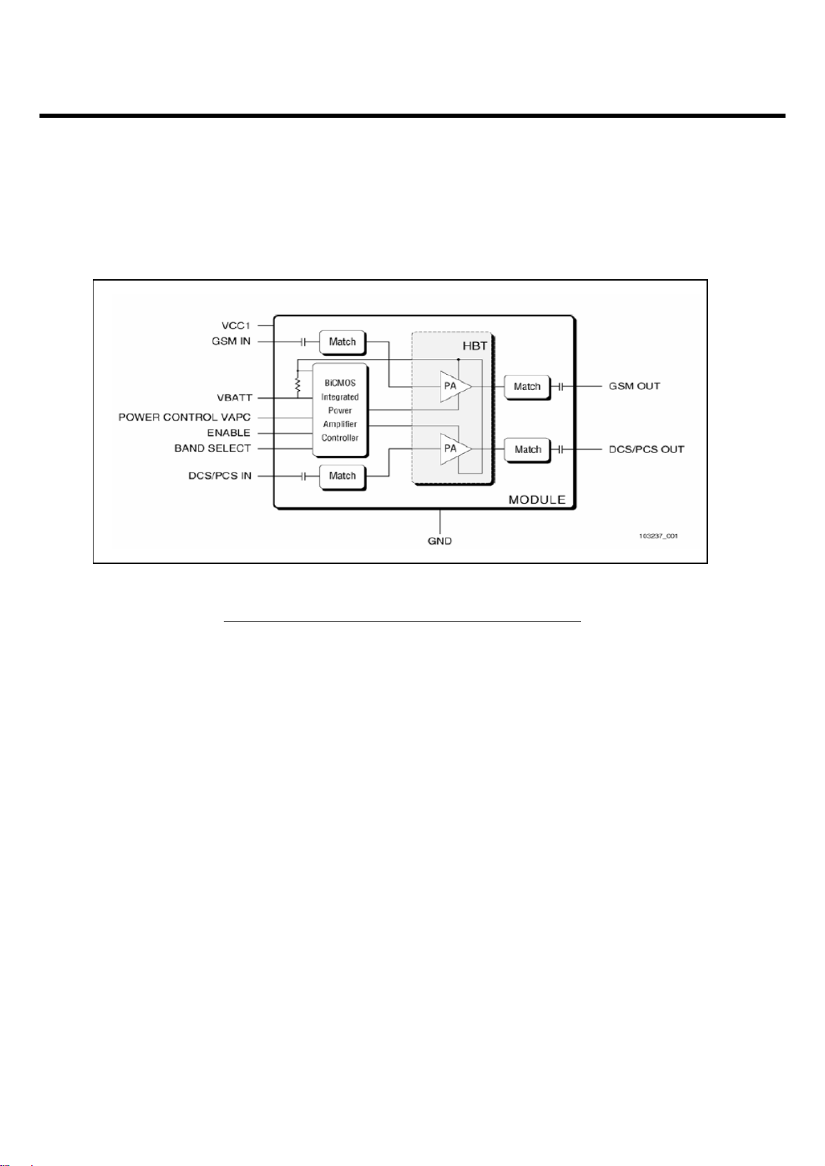
3.2 Power Amplifier Module (SKY77318)
The SKY77318 Power Amplifier Module (PAM) is designed in a low profile (1.2 mm), compact form
factor for quad-band cellular handsets comprising GSM850/900, DCS1800, and PCS1900 operation.
The PAM also supports Class 12 General Packet Radio Service (GPRS) multi-slot operation.
The module consists of separate GSM PA and DCS1800/PCS1900 PA blocks, impedance-matching
circuitry for 50 Ω input and output impedances and a Power Amplifier Control (PAC) block with an
internal current-sense resistor. The custom BiCMOS integrated circuit provides the internal PAC
function and interface circuitry. Fabricated onto a single Gallium Arsenide (GaAs) die, one
Heterojunction Bipolar Transistor (HBT) PA block supports the GSM bands and the other supports the
DCS1800 and PCS1900 bands. Both PA blocks share common power supply pins to distribute
current.
The GaAs die, the Silicon (Si) die, and the passive components are mounted on a multi-layer laminate
substrate. The assembly is encapsulated with plastic overmold.
RF input and output ports of the SKY77318 are internally matched to a 50 load to reduce the number
of external components for a quad-band design. Extremely low leakage current (2.5 µA, typical) of the
dual PA module maximizes handset standby time. The SKY77318 also contains band select switching
circuitry to select GSM (logic 0) or DCS/PCS (logic 1) as determined from the Band Select (BS) signal.
3. TECHNICAL BRIEF
- 22 -
Figure. 3-2 SKY77318 FUNCTIONAL BLOCK DIAGRAM

LGE Internal Use Only
Copyright © 2007 LG Electronics. Inc. All right reserved.
Only for training and service purposes
3. TECHNICAL BRIEF
- 23 -
In Figure 1 below, the BS pin selects the PA output (DCS/PCS_OUT or GSM_OUT) and the Analog
Power Control (VAPC) controls the level of output power.
The VBATT pin connects to an internal current-sense resistor and interfaces to an integrated power
amplifier control (iPAC
TM
) function, which is insensitive to variations in temperature, power supply,
process, and input power.
The ENABLE input allows initial turn-on of PAM circuitry to minimize battery drain.
LGE Internal Use Only
Copyright © 2007 LG Electronics. Inc. All right reserved.
Only for training and service purposes
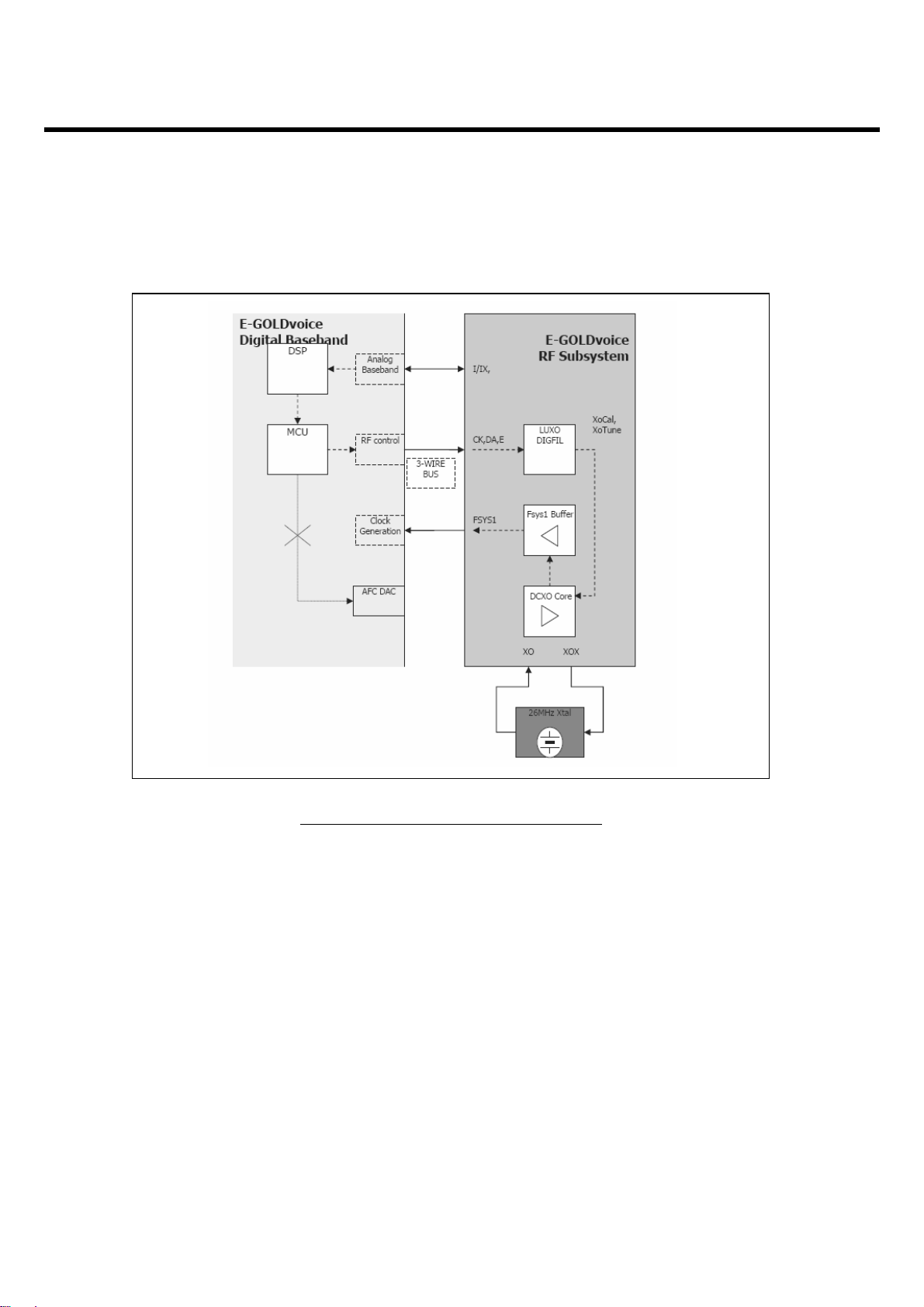
3.3 26 MHz Clock (DCXO)
DCXO (Digitally Controlled Crystal Oscillator) and VCTCXO (Voltage Controlled Temperature
Compensated Crystal Oscillator) are two different techniques used to maintain the mobile’s reference
oscillator’s accuracy over time. The reference oscillator’s accuracy over time will vary due to initial
crystal frequency offset, temperature drift and aging. These static and dynamic frequency variations
have to be compensated, otherwise the mobile would be in danger of losing connection to the network.
The technique used to perform the frequency compensation is generally termed Automatic Frequency
Control (AFC). To summarize the operation of DCXO, GSM Baseband processor will calculate the
AFC compensation (which is continuously updated) required based on the measured frequency error.
Then the required AFC compensation is sent to the LUXO (Lineari-Zation Unit of Crystal Oscillator),
which in turns control the DCXO core and generates the 26MHz system clock.
3. TECHNICAL BRIEF
- 24 -
Figure. 3-3 E-Glod Voice DCXO Overview
LGE Internal Use Only
Copyright © 2007 LG Electronics. Inc. All right reserved.
Only for training and service purposes
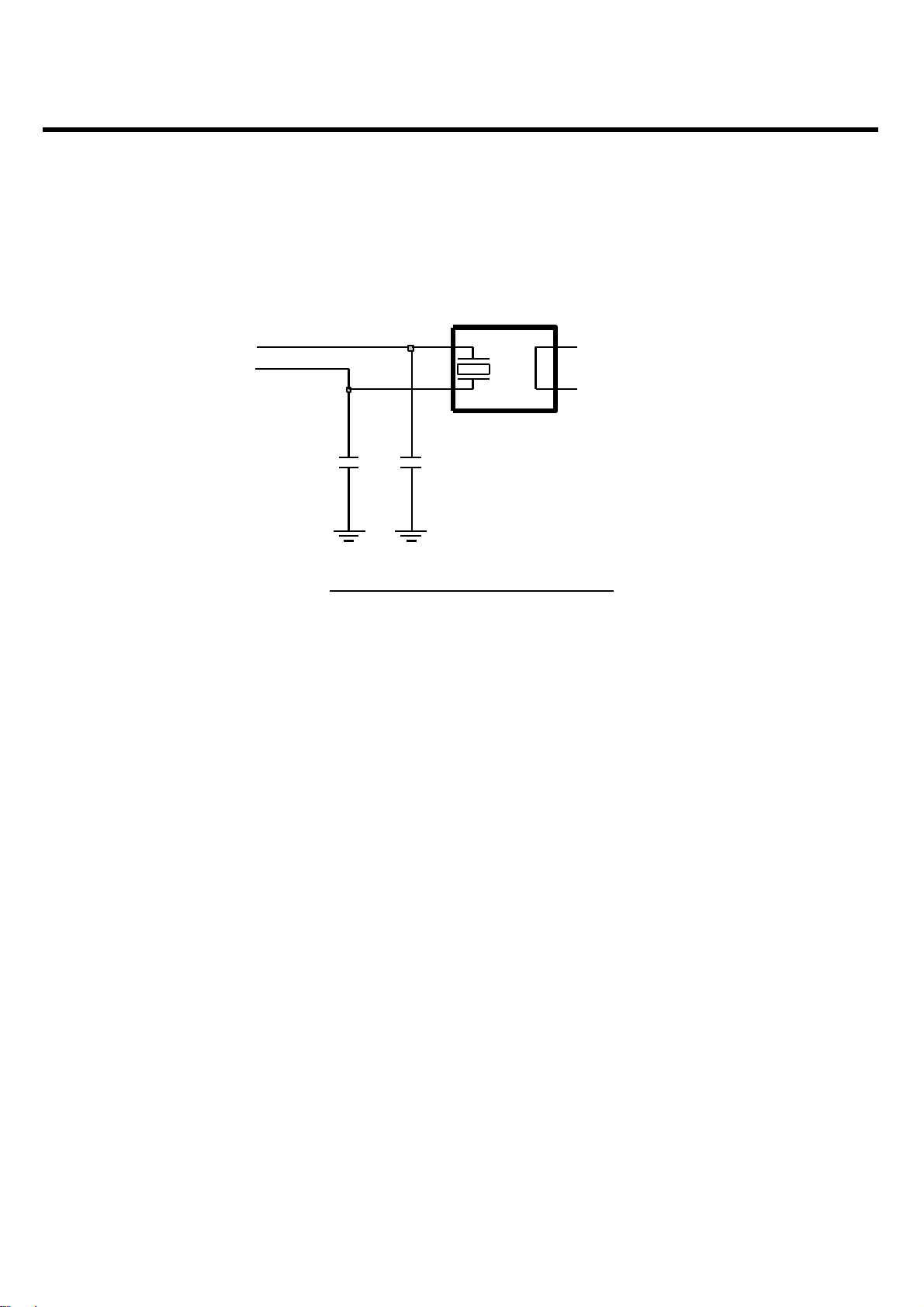
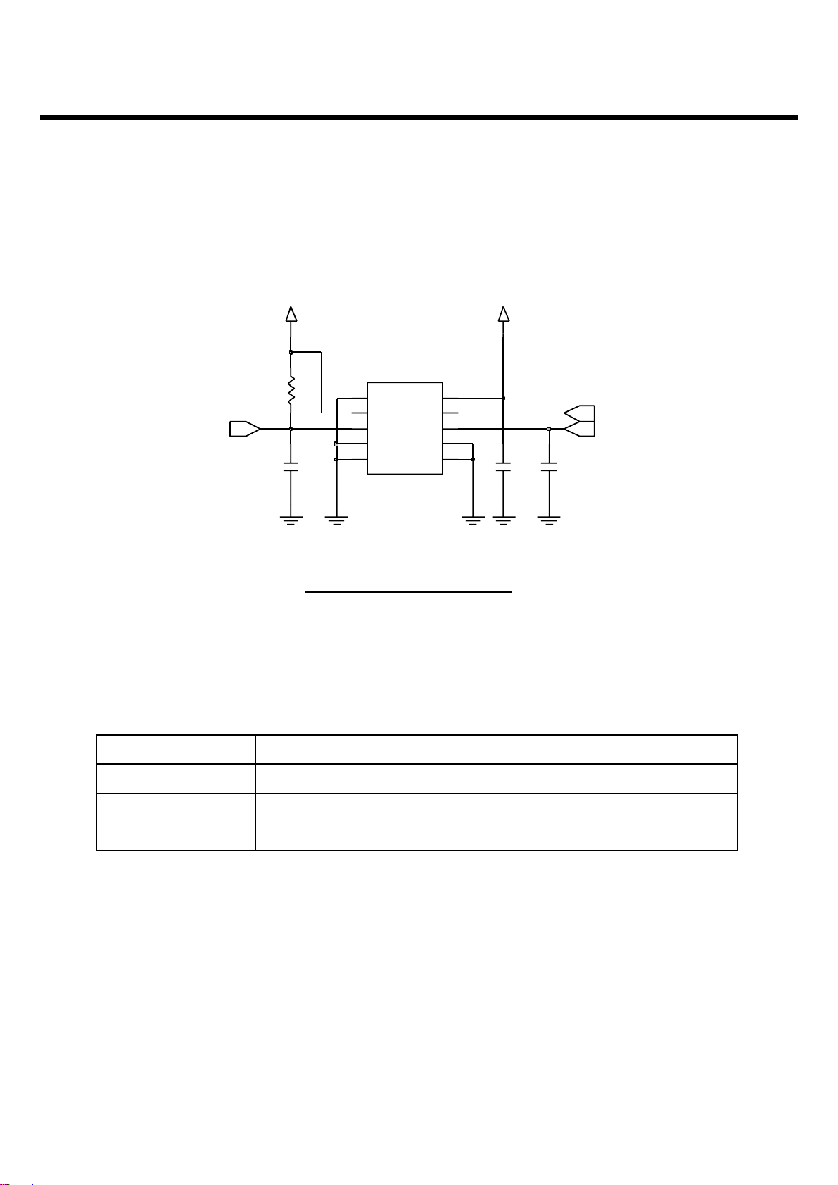
3.4 RTC(32.768KHz Crystal)
The integrated Real Time Clock (RTC) is able to provide programmable alarm functions and external
interrupts. Due to its extreme low power consumption the RTC can be supplied from a small backup
battery. This allows the generation of external interrupts, even when the main PMB7880 supply
voltage is switched off. For this purpose the RTC is powered by own voltage supply pins VDD_RTC
and VSS_RTC.
The RTC shall be driven by a 32.768 kHz (32k) clock which needs to be applied via the PMB7880
F32K and OSC32K pins. The clock can be fed from either an external clock source or use the on chip
32 KHz oscillator module.
The low clock frequency and the optimized low power design give the possibility to run the chip with a
minimum of power dissipation. For example, for this specific application the 26 MHz reference
oscillator can be switched off during system standby and a low- power time reference can be kept
when the 32k clock is provided to the RTC.
The RTC consists of an PMB7880 specific RTC shell, containing the RTC macro, as well as the 32
kHz oscillator, as described in the following sections. The module RTC Shell solely performs level
translation of the 32KHz clock to the VDD_LD1 power supply domain, and is not functionally
associated with the RTC.
3. TECHNICAL BRIEF
- 25 -
Figure. 3-4 E-Gold Voice RTC Interface
32.768KHz
MC-146_12_5PFX101
12
3
4
C121
18p
C122
18p
LGE Internal Use Only
Copyright © 2007 LG Electronics. Inc. All right reserved.
Only for training and service purposes
3.5 LCD Interface(3-wire SPI interface)
3. TECHNICAL BRIEF
- 26 -
Figure 3-5-1. LCD Interface
VBAT
10
INOUT_B4
INOUT_B5
9
8
INOUT_B6
7G114
G2
INOUT_A1
1
2
INOUT_A2
3
INOUT_A3
INOUT_A4
4
5
INOUT_A5
INOUT_A6
6
13
INOUT_B1
INOUT_B2
12
INOUT_B3
11
ICVE31186E150R101FR
FL200
18
19
20
21
22
23
24
2
3
4
5
6
7
8
9
16
25
26
27
28
29
30
17
CN200
1
10
11
12
13
14
15
C221
1000p
VA202
2V85_VIO
INOUT_B3
INOUT_B4
10
9
INOUT_B5
INOUT_B6
8
FL201
ICVE31186E150R101FR
G17G2
14
1
INOUT_A1
INOUT_A2
2
INOUT_A3
3
4
INOUT_A4
INOUT_A5
5
6
INOUT_A6
INOUT_B1
13
12
INOUT_B2
11
VA201
0.1uC220
A(7)
IND_LED_B
IND_LED_R
D(0:7)
LCD_RESET
MLED
MLED2
SPK_RCV_N
SPK_RCV_P
MOTOR_P
LCD_ID
MLED1
_LCD_CS
_WR
Figure 3-5-2. Charge pump interface
1u
C205
VBAT
9
C2+
7
C2-
6
8
CP
D1
1
2
D2
D3
3
11
EN_SET
4
GND
IN
5
12
NC
U200 AAT3157ITP-T1
10
C1+
C1-
1u
C203
VA200
C219 27p
C202 0.1u
C217
2.2u
R210
100K
27pC218
MLED1
MLED2
MLED
W_LED_EN
LGE Internal Use Only
Copyright © 2007 LG Electronics. Inc. All right reserved.
Only for training and service purposes
The AAT3157 is a low noise, constant frequency charge pump DC/DC converter that uses a tri-mode
load switch (1X), fractional (1.5X), and doubling (2X) conversion to maximize efficiency for white LED
applications. The AAT3157 is capable of driving up to three channels of LEDs at 20mA per channel
from a 2.7V to 5.5V input.
The current sinks may be operated individually or in parallel for driving higher current LEDs. A low
external parts count (two 1µF flying capacitors and two small 1µF capacitors at VIN and VOUT) make
this part ideally suited for small, battery-powered applications. Analogic Tech's S2CwireTM(Simple
Serial ControlTM) serial digital input is used to enable, disable, and set current for each LED with 16
settings down to 50µA.
The low-current mode supply current can be as low as 50µA to save power.
3. TECHNICAL BRIEF
- 27 -
Figure 3-5-3. Charge pump Output Current
Signals Description
_LCD_CS This signal enable to access to the driver IC of LCD.
D[0:7] This signal transfer 8bit parallel data to driver IC.
A(7) Data / Command switch
LCD_RESET This signal makes driver IC to HW default status.
MLED This signal provide power to white LEDs.
MLED1/2 The white LED current sink ports
2V85_VIO This signal provides power to LCD modules.(2.8V)
Data Output (mA/Ch) Data Output (mA/Ch)
1 20.0 9 5.0
2 17.0 10 4.2
3 14.0 11 3.4
4 12.0 12 2.8
5 10.0 13 1.0
6 8.6 14 0.5
7 7.0 15 0.1
8 6.0 16 0.05
LGE Internal Use Only
Copyright © 2007 LG Electronics. Inc. All right reserved.
Only for training and service purposes
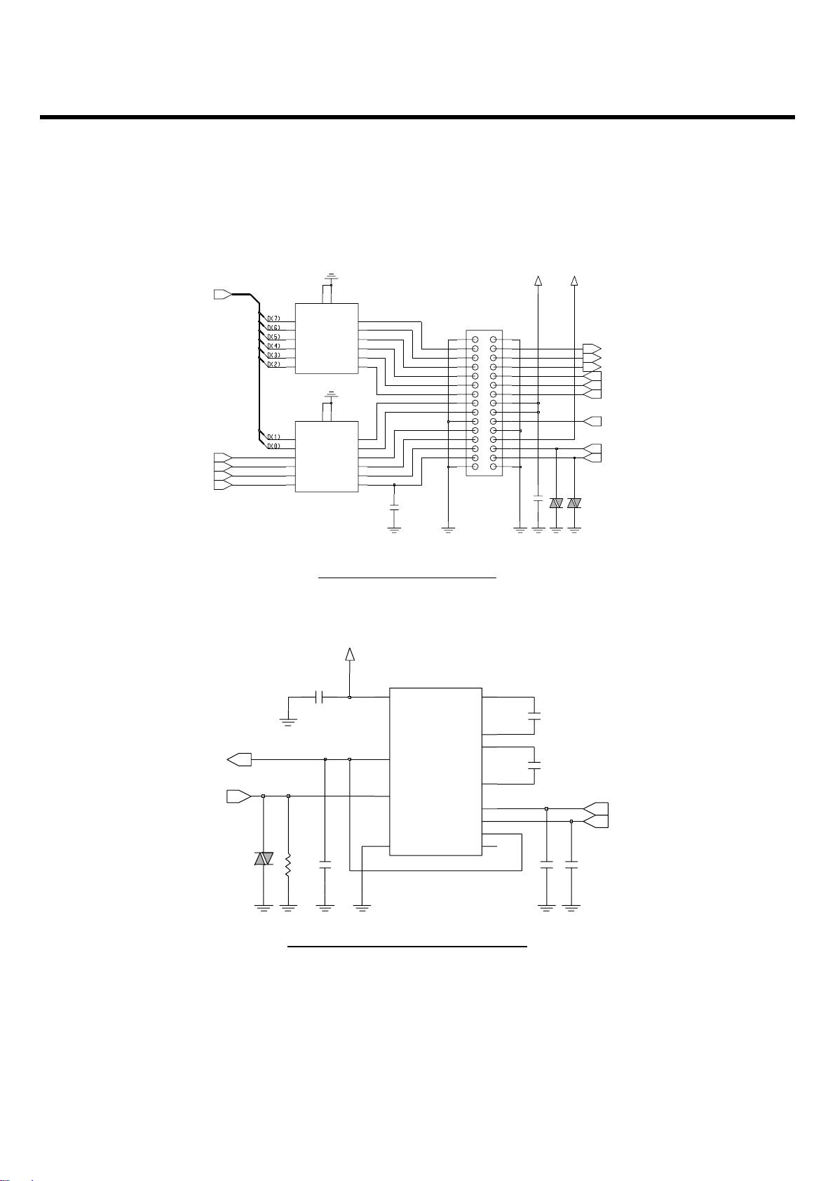
3.6 SIM Card Interface
The E-Gold Voice provides SIM Interface Module. The AD6527 checks status Periodically During
established call mode whether SIM card is inserted or not, but it doesn't check during deep sleep
mode. In order to communicate with SIM card, 3 signals SIM_DATA, SIM_CLK, SIM_RST.
3. TECHNICAL BRIEF
- 28 -
Figure 3-6. SIM CARD Interface
C124
0.1u
22p
C125
R113
4.7K
CLK
3
4
GND1
GND2
7
8
GND3GND4
9
10
GND5
IO
6
2
RST
1
VCC
VPP
5
J100
2V85_VSIM2V85_VSIM
22p
C123
SIM_DATA
SIM_CLK
SIM_RST
Signals Description
SIM_RST This signal makes SIM card to HW default status.
SIM_CLK This signal is transferred to SIM card.
SIM_DATA This signal is interface datum.
LGE Internal Use Only
Copyright © 2007 LG Electronics. Inc. All right reserved.
Only for training and service purposes
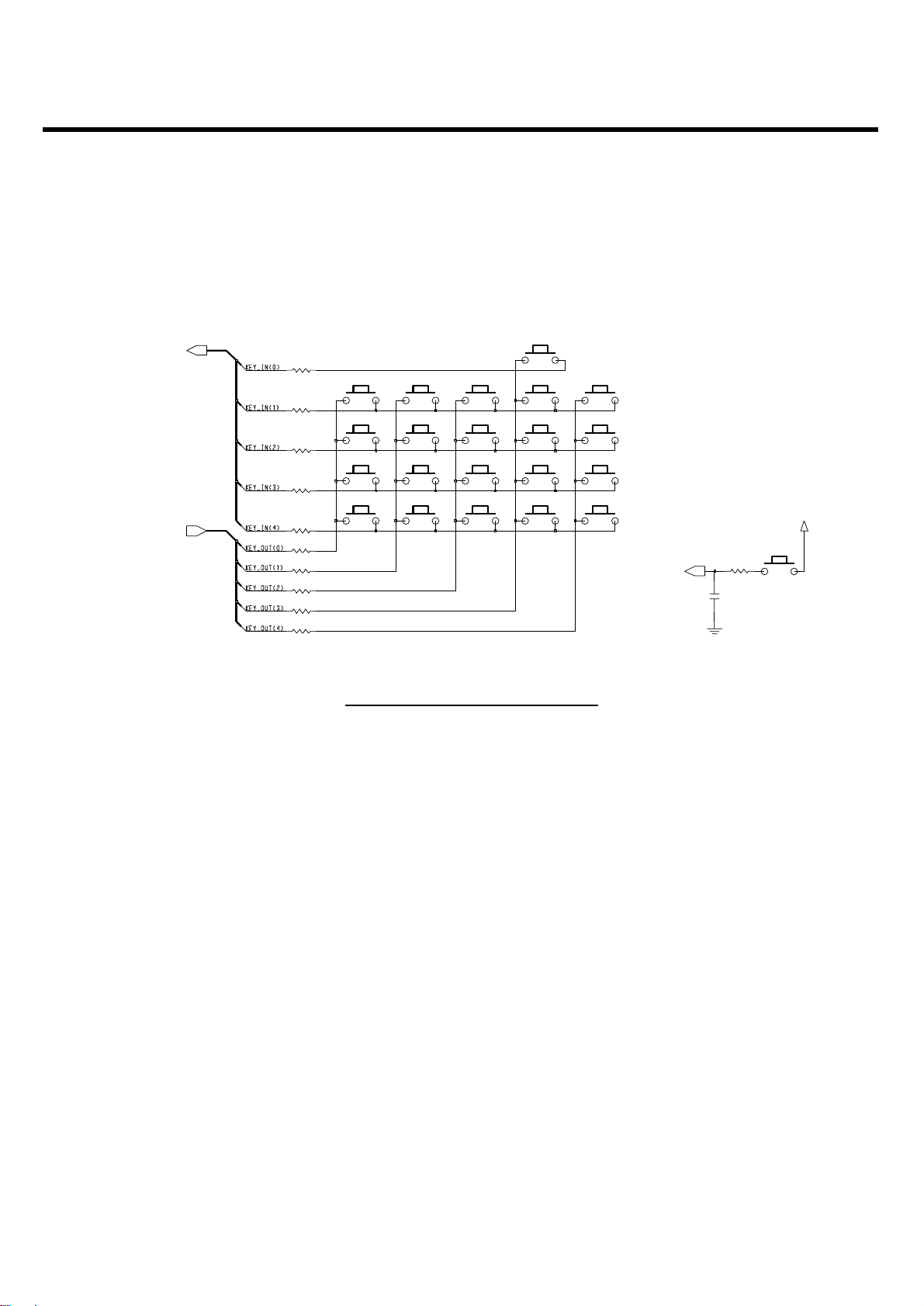
3.7 KEYPAD Interface
The keypad interface is connected to the X-Bus, together with the XBIU and the shared Memory
Register, using a single Bus Interface.
The keypad supports two scan modes:
• By default, the keypad is a 5x5 scan matrix 5 input and 5 output pins).
• To set the keypad to a 5x5 scan matrix (5 input and 5 output pins)
The scan mode should be determined at the very beginning of the system start because changes are
not allowed later.
3. TECHNICAL BRIEF
- 29 -
Figure 3-7 KEY MAXTRIX Interface
END
SEL
680
R229
R234
1K
202
UP
100p
C242
MENU
204
R232 680
207
R233 680
201
STAR
R235 680
R228
680
LEFT
CLEAR
680
R227
OK
R230
680 DOWN
R237 680
206 SEND
209
205
RIGHT
203
200
R231 680
R236 680
208
2V0_VRTC
SHARP
KEY_IN(0:4)
KEY_OUT(0:4)
PWRON
 Loading...