

Page 1
Service Manual
Service Manual
KE500/ME550c
Model : KE500/ME550c
Date: May, 2007 / Issue 1.0
Page 2

- 3 -
1. General Description........................ 5
2. Performance .................................... 6
2.1 Product Name ......................................... 6
2.2 Supporting Standard................................6
2.3 Main Parts : GSM Solution...................... 6
2.4 HW Feature..............................................7
2.6 Technical Specification ..........................12
3. Circuit Description........................ 17
3.1 General Description .............................. 17
3.2 RF Part.................................................. 17
3.3 Digital Baseband....................................24
3.4 Analog Baseband.................................. 32
3.5 Bluetooth Interface................................ 40
4. TROUBLE SHOOTING .................. 43
4.1 RF Part Technical Brief......................... 43
4.2 RF Part Trouble shooting...................... 49
4.3 Bluetooth Trouble Shooting .................. 57
4.4 Baseband Part Troubleshooting ........... 61
4.5 LCD Display Trouble............................. 68
4.6 Camera Trouble Shooting..................... 73
4.7 Flash LED Trouble Shooting................. 79
4.8 SIM Detect Trouble Shooting................ 82
4.9 Slide Up/Down and Trouble Shooting... 85
4.10 Speaker/Receiver Trouble Shooting
(Common Path)................................... 87
4.11 Speaker/Receiver Trouble Shooting
(Acoustic Path).................................... 90
4.12 MIC Trouble Shooting ......................... 91
4.13 Ear-Mic Jack Detection
Trouble Shooting................................. 93
4.14 Ear-Mic Hook Detection
Trouble Shooting................................. 94
4.15 Ear-Mic Headset MIC
Trouble Shooting................................. 95
4.16 Ear-Mic Headset HSOR/HSOL
Trouble Shooting..................................96
4.17 FM-Radio Trouble Shooting.................98
4.18 Transflash Trouble Shooting................99
4.19 Main Key Backlight LED Trouble
Shooting.............................................101
4.20 Slide Key Backlight LED Trouble
Shooting.............................................103
4.21 Vibrator Trouble Shooting..................104
5. Downloading Software ............... 105
5.1 The purpose of downloading software 105
5.2 The Environment of Downloading
Software.............................................. 103
5.3 Download Procedure ...........................107
6. BLOCK DIAGRAM ....................... 114
7. CIRCUIT DIAGRAM ..................... 117
8. PCB LAYOUT............................... 128
9. RF Calibration
...................................
139
9.1 What’s the Rx Calibration?
................
139
9.2 What’s the Tx Calibration?
................
139
9.3 Calibration program - HOT_KIMCHI ..140
12. EXPLODED VIEW &
REPLACEMENT PART LIST ..... 145
12.1 EXPLODED VIEW ............................ 145
12.2 Replacement Parts
<Mechanic component>.................... 147
<Main component> ........................... 151
12.3 Accessory ......................................... 166
Table of Contents
Page 3

Page 4

1. General Description
- 5 -
The information in this manual is subject to change without notice and should not be construed as a
commitment by LGE Inc. Furthermore, LGE Inc.
reserves the right, without notice, to make changes to equipment design as advances in engineering
and manufacturing methods warrant.
✻ This manual provides the information necessary to install, program, operate and maintain the
ME550c.
1. General Description
Page 5
2. Performance
- 6 -
2. Performance
2.1 Product Name
ME550c : GPRS Class 10 / EDGE Class 10
2.2 Supporting Standard
2.3 Main Parts : GSM Solution
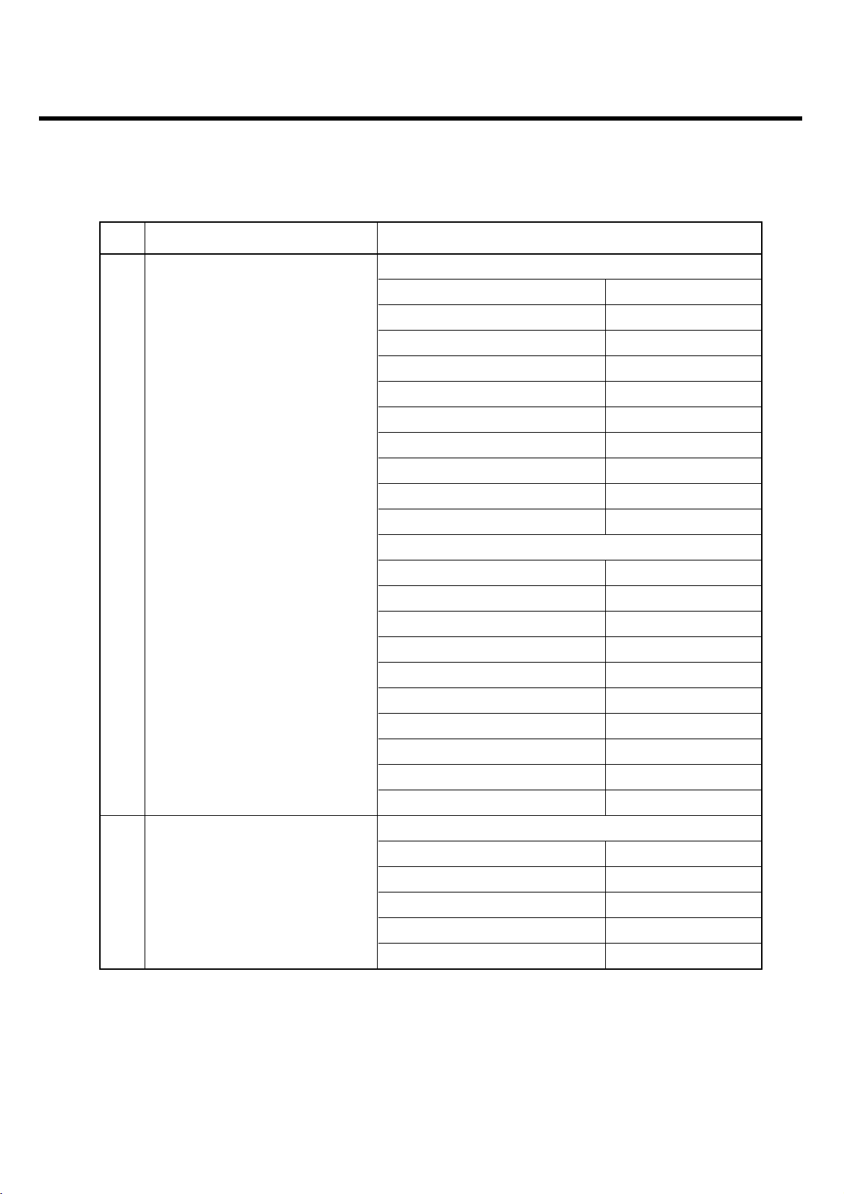
Item Feature Comment
Supporting Standard EGSM/DCS1800/PCS1900
with seamless handover
Phase 2+(include AMR)
SIM Toolkit : Class 1,2,3,E
Frequency Range EGSM TX : 880 - 915 MHz
EGSM RX : 925 - 960 MHz
DCS1800 TX : 1710 - 1785 MHz
DCS1800 RX : 1805 - 1880 MHz
PCS1900 TX : 1850 - 1910 MHz
PCS1900 RX : 1930 - 1990 MHz
Application Standard WAP 2.0, JAVA 2.0
Item Part Name Comment
Digital Baseband Neptune (D761811BZVL): TI
Analog Baseband Triton (TWL3029): TI
RF Chip B6PLD: RENESAS
Page 6
2. Performance
- 7 -
2.4 HW Feature
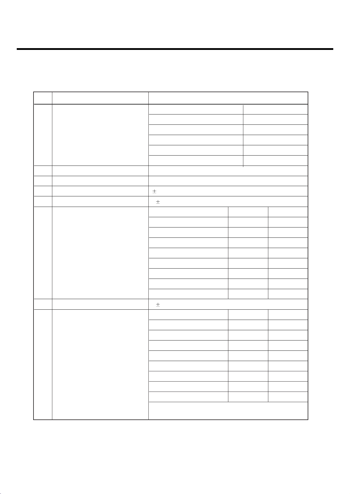
Item Feature Comment
Form Factor Slide
1) Capacity
Battery Standard : Li-Polymer, 800mAh
2) Packing Type : Hard Pack
Size
Standard :
97.0 X 47.0 X 14.9 mm
Weight 90g With Battery
Volume 75cc
PCB Staggered 10Layers , 0.8t
Stand by time 250 hrs @ Paging Period 5
Charging time 3 hrs @ Power Off / 800mAh
Talk time Min : 3.0 hrs @ Power Level 7 @ EGSM / 800mAh
EGSM : -105 dBm
RX sensitivity DCS 1800 : -105 dBm
PCS 1900 : -105 dBm
GSM/ EGSM : 33 dBm Class4 (EGSM)
GPRS DCS 1800 : 30 dBm Class1 (PCS)
TX output power
PCS 1900 : 30 dBm Class1 (DCS)
EGSM : 27 dBm E2 (EGSM)
EDGE DCS 1800 : 26 dBm E2 (PCS)
PCS 1900 : 26 dBm E2 (DCS)
GPRS compatibility GPRS Class 10
EDGE compatibility EDGE Class 10
SIM card type
Plug-In SIM
3V /1.8V
Main LCD
Display 262K Color TFT (176 x 220)
Backlight : White LED
Built-in Camera 2M CMOS Camera One button access
Page 7
2. Performance
- 8 -
Item Feature Comment
Status Indicator None
Alphanumeric Key : 12 Function Key:
Function Key : 9 4 Key Navigation, OK, F1,
Side Key : 4 F2, CLR, SND
Keypad
Total No of Keys :25 Side Key :
Volume up/down, CAM,
PWR/END
ANT
Main : Internal Fixed Type
Blue tooth : Internal Fixed Type
System connector 18 Pin
Ear Phone Jack 18pin, 4 Pole, Stereo
PC synchronization Yes
Memory
NAND Flash : 1Gbit
SDRAM : 512Mbit
Speech coding FR, EFR, HR,AMR
Data & Fax Built in Data & Fax support
Vibrator Built in Vibrator
Blue Tooth
V2.0, HSP, HFP, OPP, FTP(server),
BPP, A2DP, AVRCP
MIDI
(for Buzzer Function)
SW Decoded 64Poly
Music Player MP3/ AAC/AAC+ With Graphic EQ
Camcorder MPEG4, H.263, H.264
Voice Recording Yes
Speaker Phone mode
Yes
Support
Travel Adapter Yes
CDROM Yes
Stereo Headset Yes Optional
Data Cable Yes Optional
T-Flash (External Memory)
Yes Optional
Page 8
2. Performance
- 9 -
Item Feature Comment
RSSI 0 ~ 5 Levels
Battery Charging 0 ~ 4 Levels
Key Volume 0 ~ 5 Level
Audio Volume 1 ~ 5 Level
Time / Date Display Yes NITZ
Multi-Language Yes English / French
Quick Access Mode
Phone Book / Message / Camera
/ My Stuff / Favorite
PC Sync Schedule / Phonebook / MEMO /
SMS / Download(Photo, file)
Speed Dial Yes (2~9) Voice mail center -> 1 key
Profile Yes
CLIP / CLIR Yes (different melody)
Phone Book 4 Numbers + 1 Memo + 1 e-mail + Total 1000 Member
Group Select + Picture
Last Dial Number Yes (40)
Last Received Number Yes (40)
Last Missed Number Yes (40)
Search by Number/Name Name only
Group 7 Possible Rename
Fixed Dial Number Yes
Service Dial Number Yes
Own Number Yes
Voice Memo
Yes
Call Reminder Yes
Network Selection Automatic
Mute Yes
Call Divert Yes
Call Barring Yes
Call Charge (AoC) No No for Cingular
Page 9
2. Performance
- 10 -
Item Feature Comment
Call Duration Yes
SMS (EMS) 100 (10) EMS : Release4
(Except Text align)
SMS Over GPRS Yes
EMS Melody / Picture Yes
Send / Receive / Save
MMS MPEG4 / Send / Yes
Receive / Save
Long Message MAX 925 Characters
Cell Broadcast Yes
Download Over the WAP
Game YES
Calendar Yes
Memo 50
Unit Convert Currency/Area/Length/Volume/Weigh
t/Temperature/Velocity
Tip Calculator No
Wall Paper Yes Default 5ea
WAP Browser Over WAP 2.0 Up Brower Obigo Q-line
Download Melody / Yes Over WAP
Wallpaper
SIM Lock Yes Operator Dependent
SIM Toolkit Class 1, 2, 3, A-E
MMS Yes Openwave MMS Client
EONS Yes
CPHS
Yes V4.2
ENS Yes
Camera Yes 2M F/F / Digital Zoom : x4
JAVA Yes CLDC V1.1 / MIDP V2.0
Download Over WAP
Voice Dial No
Page 10
2. Performance
- 11 -
Item Feature Comment
IrDa No
V2.0
Blue tooth Yes
HSP, HFP, OPP,
FTP(server),
BPP, A2DP, AVRCP
GPRS Yes Class 10
EDGE Yes Class 10
Hold / Retrieve No
Conference Call Yes Max. 6
DTMF Yes
Memo pad Yes
TTY No
AMR Yes
Sync ML No
IM No
Email No
Page 11
2.6 Technical Specification
2. Performance
- 12 -
Item Description Specification
GSM850
TX: 824 + n x 0.2 MHz (n=1 ~ 124)
RX: TX + 45 MHz
GSM900
TX: 890 + n x 0.2 MHz (n=1 ~ 124)
890 + (n-1024) x 0.2 MHz (n=975 ~ 1023)
RX: TX + 45 MHz
1Frequency Band
DCS1800
TX: 1710 + ( n-511 ) x 0.2 MHz (n = 512 ~ 885)
RX: TX + 95 MHz
PCS1900
TX: 1850 + ( n-511 ) x 0.2 MHz
RX: 1930 + ( n-511 ) x 0.2 MHz (n = 512 ~ 810)
2 Phase Error
RMS < 5 degrees
Peak < 20 degrees
3 Frequency Error < 0.1ppm
GSM850/GSM900
Level Power Toler. Level Power Toler.
5 33 dBm 2dB 13 17 dBm 3dB
6 31 dBm 3dB 14 15 dBm 3dB
7 29 dBm 3dB 15 13 dBm 3dB
8 27 dBm 3dB 16 11 dBm 5dB
9 25 dBm 3dB 17 9 dBm 5dB
10 23 dBm 3dB 18 7 dBm 5dB
11 21 dBm 3dB 19 5 dBm 5dB
4 Power Level 12 19 dBm 3dB
DCS1800/PCS1900
Level Power Toler. Level Power Toler.
0 30 dBm 2dB 8 14 dBm 3dB
1 28 dBm 3dB 9 12 dBm 4dB
2 26 dBm 3dB 10 10 dBm 4dB
3 24 dBm 3dB 11 8 dBm 4dB
4 22 dBm 3dB 12 6 dBm 4dB
5 20 dBm 3dB 13 4 dBm 4dB
6 18 dBm 3dB 14 2 dBm 5dB
7 16 dBm 3dB 15 0 dBm 5dB
Page 12
2. Performance
- 13 -
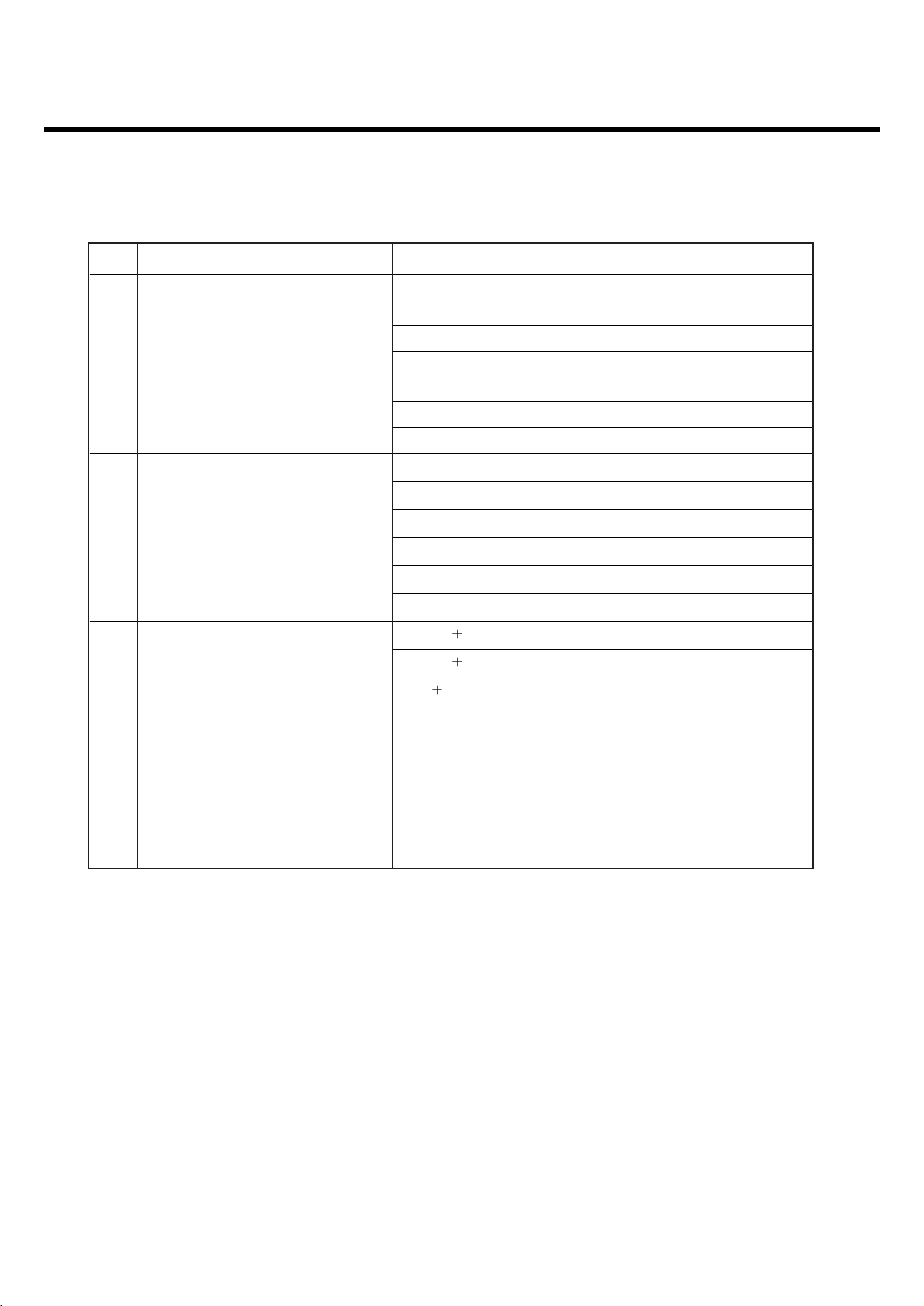
Item Description Specification
GSM900
Offset from Carrier (kHz). Max. dBc
100 0.5
200 -30
250 -33
400 -60
600~ <1,200 -60
1,200~ <1,800 -60
1,800~ <3,000 -63
3,000~ <6,000 -65
5
Output RF Spectrum 6,000 -71
(due to modulation) DCS1800/PCS1900
Offset from Carrier (kHz). Max. dBc
100 0.5
200 -30
250 -33
400 -60
600~ <1,200 -60
1,200~ <1,800 -60
1,800~ <3,000 -65
3,000~ <6,000 -65
6,000 -73
GSM900
Offset from Carrier (kHz) Max. (dBm)
Output RF Spectrum 400 -19
6
(due to switching transient) 600 -21
1,200 -21
1,800 -24
Page 13
2. Performance
- 14 -
Item Description Specification
DCS1800/PCS1900
Offset from Carrier (kHz). Max. (dBm)
Output RF Spectrum 400 -22
6
(due to switching transient) 600 -24
1,200 -24
1,800 -27
7 Spurious Emissions Conduction, Emission Status
8Bit Error Ratio BER (Class II) < 2.439% @-102dBm
9 Rx Level Report accuracy 3 dB
10 SLR 8 3 dB
Frequency (Hz) Max.(dB) Min.(dB)
100 -12 -
200 0 -
300 0 -12
11 Sending Response 1,000 0 -6
2,000 4 -6
3,000 4 -6
3,400 4 -9
4,000 0 -
12 RLR 2 3 dB
Frequency (Hz) Max.(dB) Min.(dB)
100 -12 -
200 0 -
300 2 -7
500
*
-5
13 Receiving Response 1,000 0 -5
3,000 2 -5
3,400 2 -10
4,000 2
*
Mean that Adopt a straight line in between 300 Hz and
1,000 Hz to be Max. level in the range.
Page 14
2. Performance
- 15 -
Item Description Specification
14 STMR 13 5 dB
15 Stability Margin > 6 dB
dB to ARL (dB) Level Ratio (dB)
-35 17.5
-30 22.5
-20 30.7
16 Distortion
-10 33.3
0 33.7
7 31.7
10 25.5
17 Side Tone Distortion Three stage distortion < 10%
18
<Change> System frequency
2.5ppm
(13 MHz) tolerance
19 <Change>32.768KHz tolerance 30ppm
Full power
- 340mA(GSM900), < 260mA(DCS/PCS)
20 Power consumption Standby
- Normal mode ? 4.0mA(Max.power)
- Using Test mode on DSP Sleep function ? 6mA
GSM900/Lvl 7 (Battery Capacity 800mA) : 180 min
20 Talk Time
GSM900/Lvl 12 (Battery Capacity 800mA) : 300 min
PCS1900/Level5 (Battery 800mA) : 310 Min
PCS1900/Level10(Battery 800mA) : 390 Min
Under conditions, at least 200 hours:
1. Brand new and full 800mAh battery
2. Full charge, no receive/send and keep GSM in idle mode.
21 Standby Time
3. Broadcast set off.
4. Signal strength display set at 3 level above.
5. Backlight of phone set off.
At least 70 dB under below conditions:
22 Ringer Volume 1. Ringer set as ringer.
2. Test distance set as 50 cm
23 Charge Voltage
Fast Charge : < 550 mA
Slow Charge: < 60 mA
Page 15
2. Performance
- 16 -
Item Description Specification
Antenna Bar Number Power
5-85 dBm ~
4-90 dBm ~ -86 dBm
24 Antenna Display 3 -95 dBm ~ -91 dBm
2-100 dBm ~ -96 dBm
1-105 dBm ~ -101 dBm
0~ -105 dBm
Barttey Bar Voltage
0(included Blinking) 3.65V~3.35V
1 3.71V ~ 3.66V
25 Battery Indicator
2 3.78V ~ 3.72V
3 3.91V ~ 3.79V
4 4.20V ~ 3.92V
26 Low Voltage Warning
3.60V↓ 0.03V (Standby)
3.50V↓ 0.03V (Call)
27 Forced shut down Voltage 3.35 0.03 V
1 Li-polymer Battery, Hardpack
28 Battery Type
Standard Voltage = 3.7 V
Battery full charge voltage = 4.2 V
Capacity: 800mAh
Switching-mode charger
27 Travel Charger Input: 100 ~ 240 V, 50/60Hz
Out put: 4.8V, 900mA
Page 16
3. Circuit Description
- 17 -
3. Circuit Description
3.1 General Description
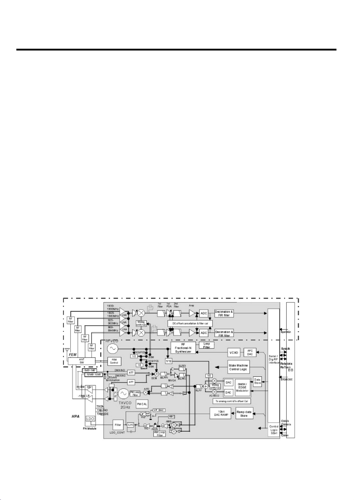
The RF part consists of a transmitter, a receiver, a synthesizer, a voltage supply and a DCXO part.
The main RF Chipset B6PLD is a highly integrated RF tranceiver IC FOR Digital Interface of GSM 850,
GSM900, DCS1800 and PCS1900 quad-band cellualr systems. The B6PLD incorporates EDGE
tranceiver apability, quad R low-noise amplifiers(LNSa). Direct conversion mixers, a programmable
gain amplifier(PGA) with DC offset and frequency response correction, ADC, Digital filiter, Digital
Interface, fully integrated VCOs, an RF fractiona-N synthesiser, a low-noise offset PLL transmitter,
Digital modulator, TXDAC, RAMPDAC, and AFCDAC. The B6PLD includes state machine control
through serial programming. All functions operate down to 2.67V and are housed in a 72-pin BGA
package. Hence the B6PLD can form a small size transceiver handset for quad band EDGE
tranceiver.
3.2 RF Part
3.2.1 Receiver Part
The B6PLD receiver supports quad band, so the front-end incorporates four LNAs and two mixers.
The incoming RF signals are mixed directly down to I/Q baseband by the front-end bolck. This
incorporates four LNAs/four buffers and two Gillbert Cell mixer blocks optimised for operation at
850MHz, 900MHz, 1800MHz and 1900MHz respectively. The front-end block is followed by two
closely matched baseband amplifier chains. These include distributed low pass filtering, one switched
gain stage and one fixed gain stage. In addition, the baseband section integrates A/D and D/A
converters which provide automatic on-chip correction of DC offsets.
<Fig.1> Receiver Part Block Diagram
Page 17

3.2.1.1 Baseband PGA/Low pass Filter Specifications
The baseband programmable amplifier comprises one stage with variable gain followed by a fixed
gain amplifier. The overall gain control range is 36dB with 6dB Steps. The filtering is provided by a
single R/C low pass filter with an on-chip capacitor followed by on-chip Chebychev low pass filters.
The filters have been specified to achieve maximal group delay flatness in the pass-band combined
with the required levels of suppression of interfering signals. The distribution of the gain and filtering
has been designed to ensure that the receiver does not compress under blocking conditions. The
final fixed gain amplifier is included to match the on-chip levels to the input dynamic range of the
ADC.
3.2.1.2 DC offset auto-calibration system
B6PLD implements a system for cancelling the DC offsets in the baseband programmable gain
amplifiers(PGA). This prevents a small DC offset at the input giving a large DC offset at the output,
even at high gain settings. When the B6PLD receiver is performing an auto-calibration, the
sequencer cancels the offsets locally around the PGA, then the Digital filter. The system includes
switches to short out the signal path whilst the cancellation is occurring. The switches are opened in
sequence as the calibration progresses. For PGA the A/D converter system employs a successive
approximation technique and achieves 6 bit resolution. The PGA stage has an associated 6 bit
current DAC which cancels the DC offset at the output. The sequencer ensures that on-chip filters
have sufficient time to settle before applying correction in the next digital offset cancellation stage.
3. Circuit Description
- 18 -
Page 18
3. Circuit Description
- 19 -
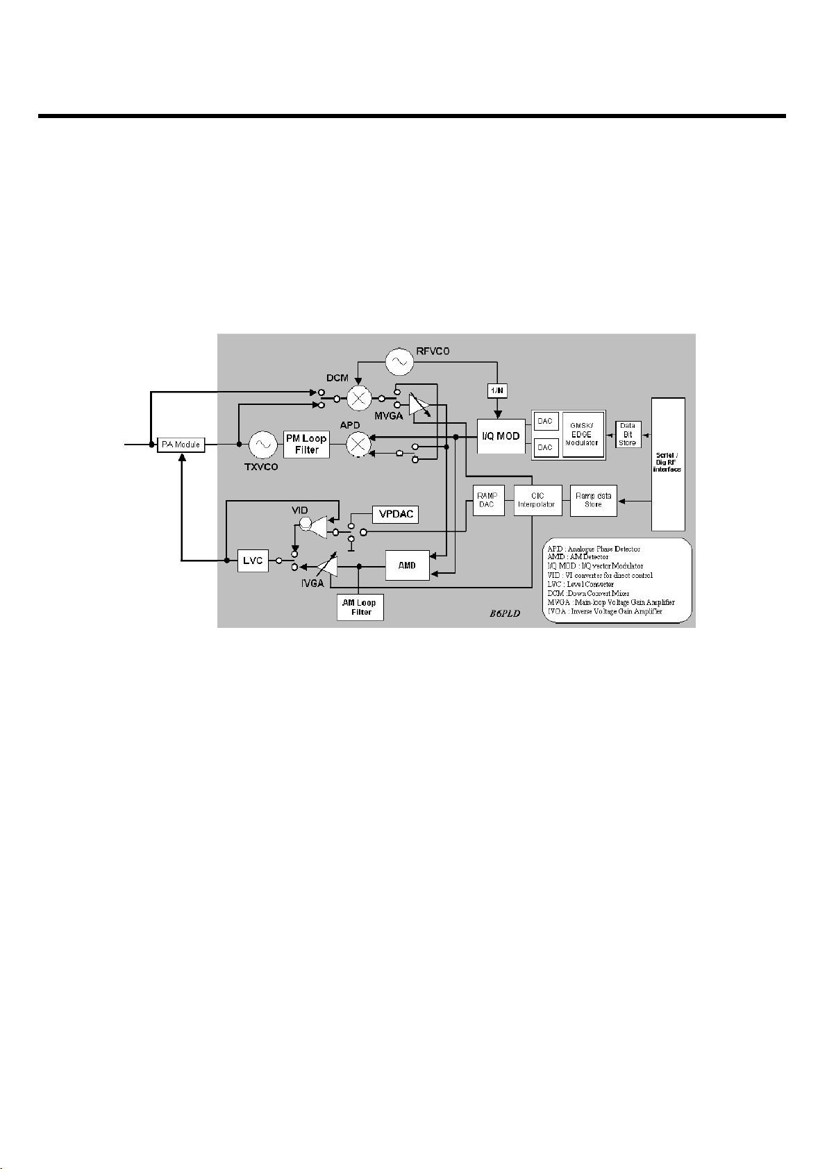
3.2.2 Transmitter part
The B6PLD transmitter is capable of both GMSK and 8-PSK modulation, to support for conventional
GSM and EDGE. B6PLD integrates all loop filters to configure both PM loop and AM loop. See block
diagram below.
3.2.2.1 Polar Loop Structure
Three main functions are identified in the transmitter architecture; I/Q vector modulation at IF
frequency, amplitude and phase loop at IF/RF frequencies and power amplification.
Fig. Simplified Block diagram for Tx part
Page 19
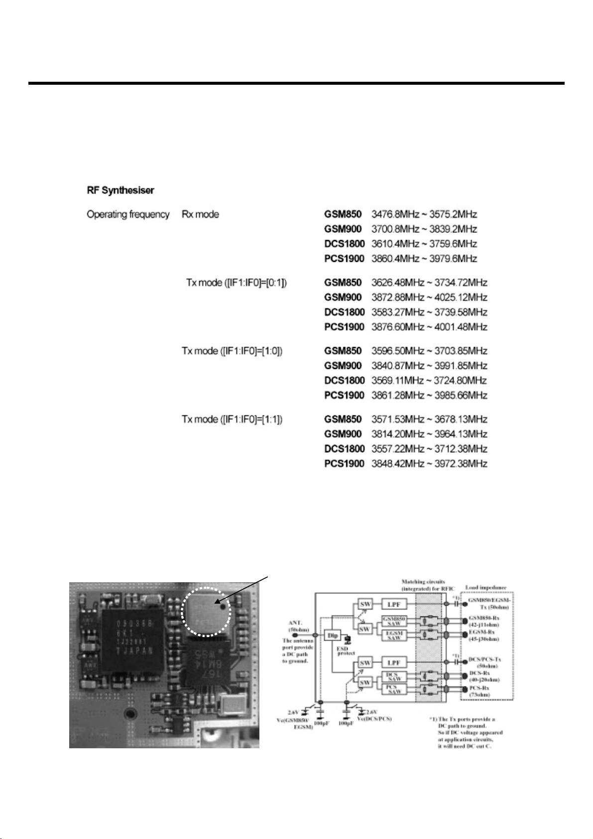
3.2.3 RF Systhesiser
3.2.4 Front End Module Specification
3.2.4.1 Block Diagram and Internal Matching Condition
3. Circuit Description
- 20 -
HWXR693
Page 20
3. Circuit Description
- 21 -
3.2.4.2 Logic Table for Selction
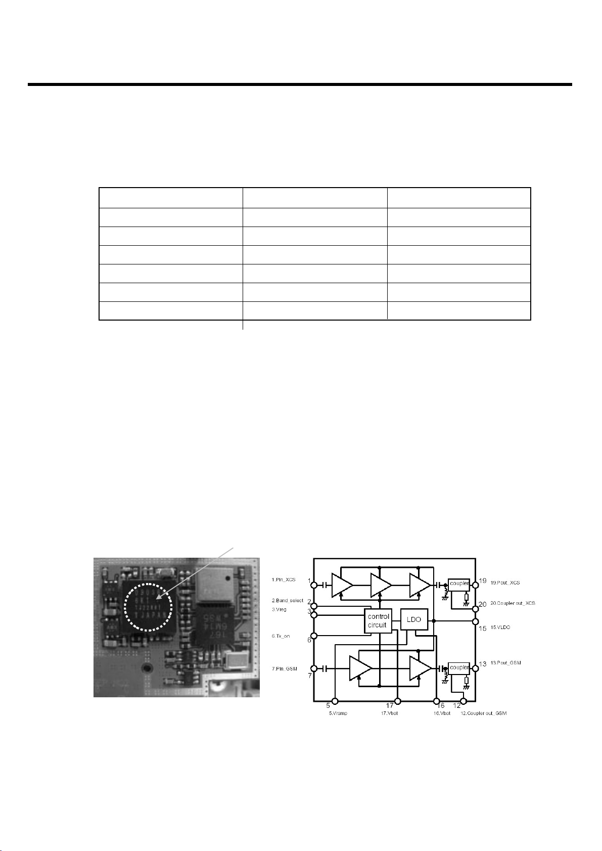
3.2.5 Power Amplifier Module
for Quad-band GSM/GPRS/EDGE
3.2.5.1 PAM Specification
-. Quad band GSM, GPRS & Ploar Loop EDGE Amplifier
-. For 3.5V nominal operation
-. Bulit-in LDO circuit
-. GPRS Class 12 operation compatible
-. Integrated directional coupler
3.2.5.2 Circuit Diagram and peripheral components
Select Mode Vc(GSM850/EGSM) Vc(DCS/PCS)
GSM850_Rx Low Low
EGSM_Rx Low Low
GSM850/EGSM_Tx High Low
DCS_Rx Low Low
PCS_Rx Low Low
DCS/PCS_Tx Low High
<Table> Band SW Logic Table
RPF09036B
Page 21
3.2.6 Digital Core
3.2.6.1 Digital Interface Block Diagram
3. Circuit Description
- 22 -
Fig. 1-1 Digital Interface Block Digram
Page 22

3. Circuit Description
- 23 -
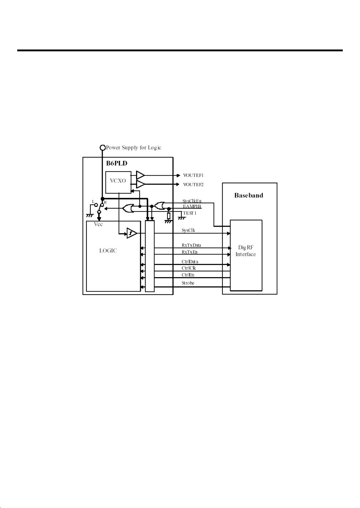
3.2.6.2 Control system and digital interface
The B6PLD is a RF transceiver IC for GSM850, GSM900, DCS1800 and PCS1900 quad band
cellular system, and incorporates EDGE transceiver capability. The B6PLD has a digital interface
connection to the baseband processor. This interface complies with the digital interface specification
DigRF standard v112.
The digital interface consists of two separate interface connections; (1) the control interface, (2) the
data interface, and a system clock on/off control signal and a precise timing singal. These are
realized by eight signal lines in B6PLD(Look at Fig1.1 above)
- The control interfce is used to configure the B6PLD for RX and TX operation, transfers of control
data for several built-in circuits, and for triggering the events. The control interface comprise a bidirectional 3-wire serial interface with the three signal lines CtrlData, CtrlEn and CtrlClk accessing
the control registers in B6PLD by transferring the control words.
- The data interface is used to transfer transmit modulation symbols and receive IQ-sampling data.
The data interface comprises a single serial bus with the three signal lines RxTxData, RxTxEn and
SysClk. The SysClk is used for system clock to baseband.
- The SsClkEn signal enables the SysClk output and powers the 26MHz oscillator on. When the
SysClkEn is negated, the SysClk is held low, and if the TEST1 pin is low by the default settings, the
logic power supply by typical 1.8 volts to the internal core logic circuits is also switched off.
Page 23
3.3 Digital Baseband
3.3.1 General description
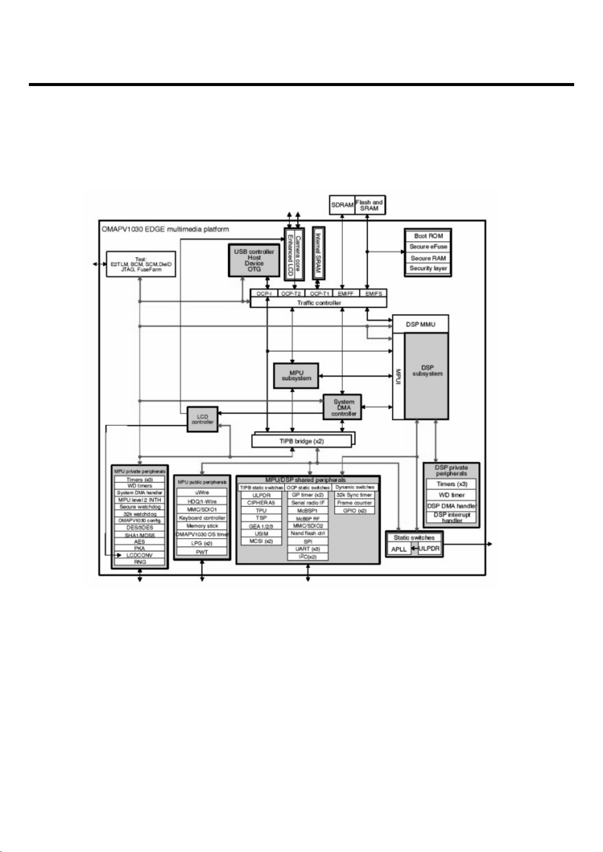
The OMAPV1030 E-GPRS multimedia device belongs to the Texas Instruments OMAP-Vox_
processors family. It combines both a modem engine and an application engine. Memory and CPU
resources are shared between modem and application processing.
The OMAPV1030 chip is based on the OMAP3.4 architecture and integrates two processor
subsystems:
- An MPU subsystem based on an ARM926EJ-S
- A DSP subsystem based on a UMA 2.6 architecture integrating a C55x DSP core The
OMAPV1030’s silicon process technology is a c027.0 90-nm digital CMOS.
3. Circuit Description
- 24 -
<Fig.6> OMAPV1030 Block Diagram
Page 24
3.3.2 Block Description
The OMAPV1030 E-GPRS multimedia device is based on an OMAP3.4 platform that integrates:
- The MPU subsystem
- The DSP subsystem
- A system DMA
- A traffic controller providing:
- External memory interfaces with:
- A slow interface (EMIFS) to ROM, SRAM, FLASH memories
- A fast interface (EMIFF) to SDRAM memories
- Layer 3 (L3) interconnect made of two OCP target ports (OCP-T1 and OCP-T2) and one OCP
initiator port (OCP-I)
- Layer 4 (L4) interconnect made of two DSP peripheral busses (private DSP TIPB and shared DSP
TIPB) and two MPU peripheral busses (public MPU TIPB and private MPU TIPB)
- Clock management
- A set of processor peripherals:
- Three 32-bit timers, a 16-bit Watchdog timer, and an interrupt handler for the MPU
- Three 32-bit timers, a 16-bit Watchdog timer, and a 2nd-level interrupt handler for the DSP
- Test and debug interfaces (JTAG, Window Tracer)
- Trace capabilities: ETM9 and Ctools
The other OMAPV1030 modules or subsystems are connected to the OMAP3.4 platform through the
L3 and L4 interconnects.
3. Circuit Description
- 25 -
<Fig.7> OMAPV1030 Top-Level Architecture Overview
Page 25

The OMAP3.4 platform is the computing core of the device. The other OMAPV1030 components are
organized as follows:
- The internal memory subsystem is made of a single-port 256K-bit shared internal SRAM.
- The security subsystem is a set of several components, including dedicated a secure mode to run
secure applications.
- A master-slave USB module provides an external interface supporting high data transfer rates
between the OMAPV1030 and external application
- The memory interfaces provide access to external memories. There are two types of memory
controllers:
- SDRAM controller supporting SDR and DDR modes
- General-purpose controller supporting asynchronous and synchronous
- The system components are used to manage system interactions such as interrupts, clock control,
reset control, and idle management.
- The peripheral subsystem refers to all the peripherals accessible by the MPU and/or the DSP. They
are all OCP- or TIPB-compliant and are connected to the OMAP3.4 platform through the traffic
controller or the TIPB busses.
3.3.3 RF Interface (Digital RF Interface)
The OMAPV1030 radio interface module of OMAPV1030 device is an interface that carries the
following information:
- Transmit symbols from DBB to RF IC
- Receive samples from RF IC to DBB
- Bidirectional information control
- Real-time and activation signals from DBB to RF IC
- System clock
The OMAPV1030 radio interface module of OMAPV1030 device supports two types of radio
interfaces.
They differ mainly in the type of data interface:
- The first interface is based on a standard six-wire scheme: three wires for transmit and three for
receive.
- The second one is based on a two-wire bidirectional scheme: one wire for data in/out, and one for
control receive/transmit.
3. Circuit Description
- 26 -
Page 26
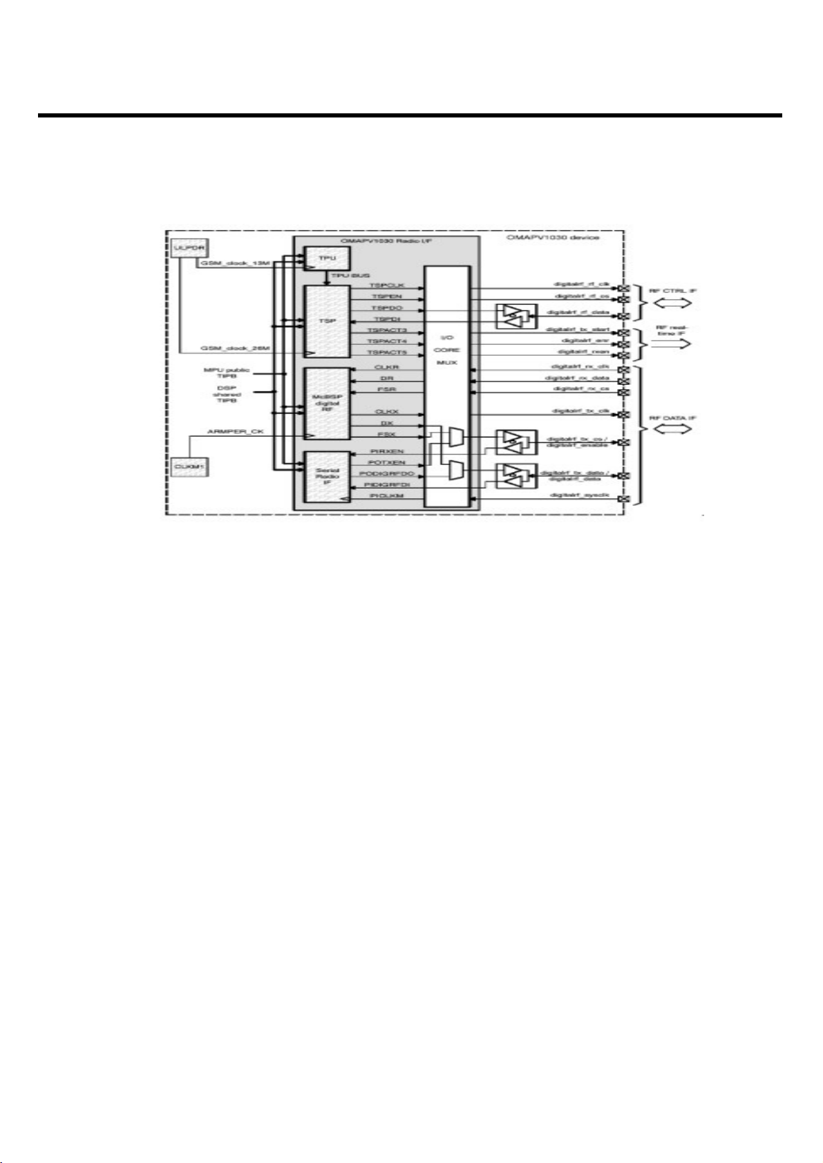
This implementation is based on the following:
- The time processing unit (TPU) module is a real-time sequencer dedicated to monitoring GSM
baseband processing.
- The serial port of the time serial port (TSP) module controls both interfaces.
- The real-time TSPACT signal of the TSP module
- The McBSP digital RF module is used for the six-wire data interface.
- The serial radio interface module is used for the two-wire data interface.
- A system clock interface receives a squared 26-MHz clock from the RF IC.
3. Circuit Description
- 27 -
<Fig.8> OMAPV1030 Radio Interface
Page 27
3. Circuit Description
- 28 -
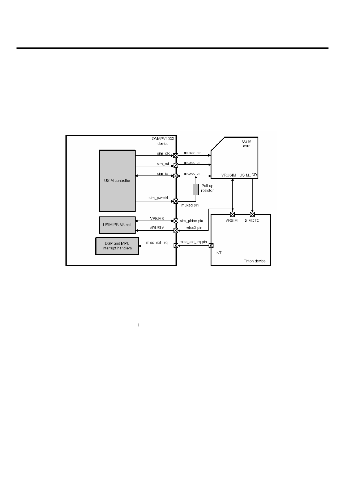
3.3.4 SIM interface
SIM interface scheme is shown in below.
SIM_IO, SIM_CLK, SIM_RST, SIM_PWRCTRL ports are used to communicate DBB via ABB with
plugged sim card and the LDO (VRSIM) in ABB enables operate 1.8V to 2.5V to search SIM card
SIM_CLK : SIM Card reference clock SIM_PWCTRL : SIM Card power activation
SIM_RST : SIM Card async/sync reset SIM_IO : SIM Card bi-directional data line
VRUSIM(Power supply VCC) : 3 V 10% (class B) or 1.8 V 10% (class C)
Misc_ext_irq : USIM card presence detection (USIM_CD) purposes.
<Fig.9> SIM Interface
Page 28
3. Circuit Description
- 29 -
3.3.5 UART Interface
ME550c has Three UART Drivers as follow :
- UART1 : USB - UART2 : ETM, Calibration - UART3 : AT command, Fax_modem, Bluetooth
UART1(USB)
Resource Name Description
USB_DP DP Data
USB_DM DM Data
USB_PWR POWER USB_POWER
VBUS VBUS USB_Detect
UART2 (ETM)
DEBUG_RX RX Receive Data(UART2)
DEBUG_TX TX Transmit Data(UART2)
UART3 (Bluetooth)
UART3_RXD UART3_RXD Receive Data
UART3_TXD UART3_TXD Transmit Data
UART3_RTS UART3_RTS Request To Send
UART3_CTS UART3_CTS Clear To Send
<Table.2> UART Interface Spec
Page 29
3. Circuit Description
- 30 -
3.3.6 GPIO Map
In total 22 allowable resources, ME550c is using 9 resources except 3 resources dedicated to SIM
and Memory. ME550c GPIO(General Purpose Input/Output) Map, describing application, I/O state,
and enable level, is shown in below table 3.
I/O # Net Name I/O
Resource Inactive Active
State State State
I/O (1) Not used
I/O (2) I Sysboot HIGH LOW
I/O (4) USB_BOOT_SEL I Sysboot LOW (Giant Plus) HIGH (Nanya)
I/O (6) I Sysboot HIGH LOW
I/O (7) DIF_VSCNC I GPIO LOW HIGH
I/O (8) BT_NRST O GPIO LOW (LCD B/L Of f ) HIGH (LCD B/L On)
I/O (9) CHG_EN O GPIO LOW HIGH
I/O (10) VCAM28_EN O GPIO LOW HIGH
I/O (12) CAM_RST O GPIO HIGH LOW
I/O (13) FM_INT I GPIO HIGH LOW
I/O (16) MAIN_KEY_BL_EN I Sysboot LOW HIGH
I/O (17) BOOT_SEL I GPIO HIGH HIGH
I/O (18) DP_PWON O GPIO LOW HIGH
I/O(27) SLIDE I GPIO LOW HIGH
I/O(32) SPK_EN O GPIO HIGH LOW
I/O (33) Not used O GPIO LOW HIGH
I/O (42) VCAM18_EN I GPIO LOW HIGH
I/O(43) CHG_STAT O GPIO HIGH LOW
I/O (46) CIF_PD I GPIO LOW HIGH
I/O (47) JACK_DETECT O GPIO HIGH LOW
I/O (55) HOOK_DETECT O GPIO HIGH LOW
I/O (63) SPK_EN O GPIO LOW HIGH
<Table.3> GPIO Map
Page 30
3. Circuit Description
- 31 -
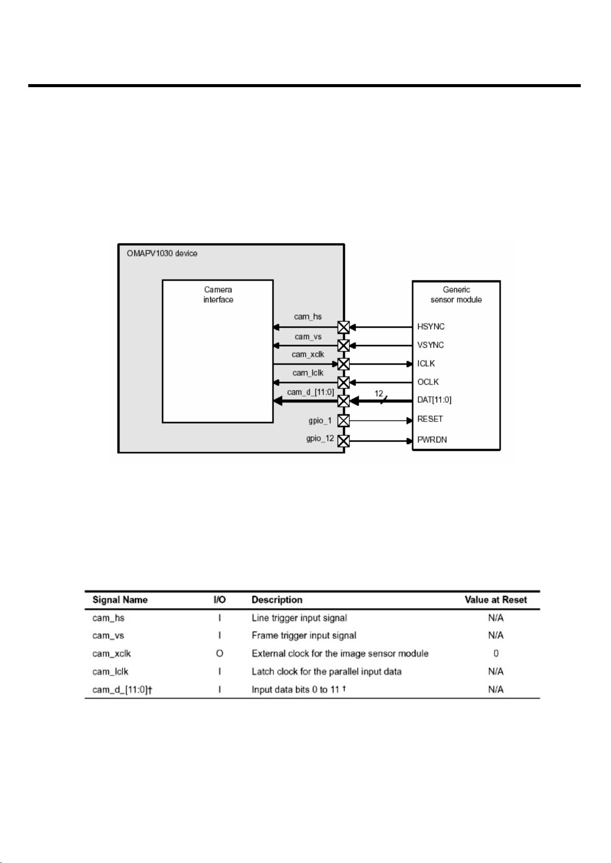
3.3.7 Camera interface
ME550c have a 8-bit parallel camera interface(NOBT Mode) .
This is a general parallel interface with vertical and horizontal synchronization signals.(See. Figure
12) The maximum clock is 96 MHz for 8-bit data data, or 48 MHz for 10- or 12-bit data.
Table7. describes the I/O signals of the generic parallel camera interface.
Figure13, Figure14 show the frame and data timing according to synchronization signals in the
parallel NOBT configuration.
<Fig.10> Generic Parallel Camera Interface
<Table 4> Generic Parallel Camera Interface
Page 31

3.4 Analog Baseband
3.4.1 General Description
The TRITON chip is the analog and power management part of the Texas Instruments next
generation wireless terminal. These GSM/GPRS/E-GPRS, 3G W-CDMA, CDMA2000 platforms are
composed of a digital baseband processor, a RF chip, an application processor OMAP and of
different peripheral devices like a LCD panel, a Multi-Media Card, a Bluetooth modem, a GPS
modem.
The purpose of the Triton device is to provide to platforms the following resources:
3. Circuit Description
- 32 -
<Fig.11> TWL3029 Architecture
- A power management system
- Power supply resources
- A voice and audio interface
- A battery charger
- A monitoring system
- A real time clock resource
- A USB 2.0 OTG transceiver with a carkit
interface
- Three White-LEDs drivers
- A vibrator driver
- A SIM-Card detection
- A thermal shutdown
- An I2C interface
- A JTAG and boundary scan
Page 32

3.4.2 Audio Signal Processing & Interface
The Audio module consists of a Voice Codec dedicated to mobile telephone terminal application and
a Stereo path.
- The Voice Codec circuit processes analog audio components in the uplink path and transmits the
converted data to the DSP speech coder through the voice serial port (VSP). In the downlink path,
the Voice Codec converts the digital samples of speech data received from the DSP via the VSP
port into analog audio signals.
The Voice Codec supports a 8kHz (default narrowband mode) to a 16kHz(wideband mode) sampling
frequency.
- The Stereo path converts audio digital samples received from the I2S serial interface into analog
audio. It supports all standard frequencies from 8kHz to 48kHz (8, 11.025, 12, 22.05, 24, 32, 44.1
and 48kHz).
- Two included PLLs provide the suitable system clocks to the Voice and Stereo circuitry (ADC,
DACS, Digital Filters, Digital interfaces). The Audio module supports 3 possible input master clocks
: 12MHz, 13MHz and 19.2MHz.
3.4.3 Power Resources
The power supply module of Triton generates the different power supplies required by Triton, the
processors and the external peripherals.
3. Circuit Description
- 33 -
Page 33

3. Circuit Description
- 34 -
<Fig.12> Power Supply Scheme
Page 34

3. Circuit Description
- 35 -
3.4.4 Monitoring ADC
The monitoring ADC (MADC) consists of a 10-bit analog-to-digital converter (ADC) combined with an
11- input analog multiplexer. The ADC implementation consists of a successive approximation
conversion.
Five of the eleven inputs are available externally (ADIN1..5), and the remaining six inputs are
dedicated to die temperature measurement, main battery voltage, backup battery voltage, charger
voltage, charger current monitoring and USB Vbus voltage. Three external inputs (ADIN1..3) are
standard inputs. The two others (ADIN4..5) which are associated with current sources, are intended
for battery temperature and battery type measurements.
3.4.5 Switch ON/OFF
ME550c Power State : Defined 4cases as follow
- Power-ON : mobile is powered by main battery or backup battery.
- Power-OFF : mobile isn’t any battery.
- Switch-ON : mobile is powered and waken up from switch-off state.
- Switch-OFF : mobile is powered to maintain only the permanent function(ULPD).
To enter into Switch-ON state, one of following 4 condition is satisfied.
- PWR-ON pushed after a debouncing time of 30ms.
- ON_REMOTE : After debouncing, when a falling edgeis detected on RPWON pin.
- IT_WAKE_UP : When a rising edge is detected on RTC_ALARM pin.
- CHARGER_IC :When a charger voltage is above VBAT+0.4V on VCHG.
<Table.5> ADC Channel Spec
ADC 8 channels
Resource Name Description
VCHG VCHG
Charging Management
VBAT VBAT
ICTL ICTL
ADIN1 TEMP_SENSE Temperature Sensing
ADIN2 JACK_TYPE Remote control’s Detect- Now No Use
ADIN3
ADIN4 REMOTE_ADC Remote control’s function
(play, stop,etc..)- Now No Use
ADIN5 BATT_TEMPS Battery Detect
Page 35

3.4.6 Memories
- 512Mbit NAND Flash + 512Mbit DDR RAM
3.4.7 LCD Module
The NM200CND module is a Color Active Matrix Liquid Crystal Display with an Light Emission Diode
(LED) Back Light system. The matrix employs a-Si Thin Film Transistor as a active element.
It is a transmissive type display operating in the normally white mode. This TFT-LCD has a 2.0 inch
diagonally measured active display area with QCIF+ resolution(176 x RGB x 220 pixels).
Each pixel is divided into Red, Green, Blue sub-pixels or dots which are arranged in vertical stripes.
Gray scale or the brightness of the dots color is determined with a 6 bit gray scale signal for each dot,
thus, presenting a palette of more than 262,144 colors.
3.4.7.1 General Description
3. Circuit Description
- 36 -
Properties Spec. of Main LCD Unit
Active screen size 31.68(H)*39.6(V) mm
Viewing area size 33.08(H)*41.0(V) mm
Color depth 262,000 colors -
Resolution 176 x RGB x 220 -
Pixel format RGB Vertical Stripe -
Dot pitch 0.06(H)*0.18(V) mm
Display operating mode Transmissive type -
User viewing angle 6 O’ clock
Page 36

3. Circuit Description
- 37 -
3.4.7.2 LCD module pin map description
Page 37

3. Circuit Description
- 38 -
3.4.8 Keypad Map description
KBC0 KBC1 KBC2 KBC3 KBC4
KBR0 1 4 7 *
KBR1 2 5 8 0
KBR2 3 6 9 3
KBR3 VOL_UP VOL_DOWN CAMERA #
KBR4 HOT_UP HOT_DOWN O.K HOT_LEFT HOT_RIGHT
KBR5 SOFT_LEFT SOFT_RIGHT SEND CLR
<Fig.13> Keypad schematic
KBR(0)
KBR(1)
KBR(2)
KBC(0)
KBC(1)
KBC(2)
KBC(3)
KBR(4)
KBR(5)
KBC(0)
KBC(1)
KBC(2)
KBC(3)
KBC(4)
R200
150
R201
150
R202
150
150R203
R204 150
R205
150
150
R206
KEYPAD
R122
R123
R124
150
R125 150
R127
150
R128
150
R129
150
17
4
201
200
258
204
VA205
VA204
EVLC5S02100
EVLC5S02100
VA100
EVLC5S02100
VA101
EVLC5S02100
203
3
207
VA206
SIDE_KEY_VOL
SIDE_KEY_CAM+PWON
S_UP
69 SHP
CN202
1
2
3
4
CN203
1
2
3
4
S_DOWN
S_MENU101
VA200
EVLC5S02100
VA201
EVLC5S02100
VA202
EVLC5S02100
VA203
EVLC5S02100
EVLC5S02100
150
150
AST
VA207
S_OK
VA210
SEND
AST
0
206
SHP209208
VA208
EVLC5S02100
VA211
202
205
S_LEFT
CLRS_MENU100
R207 150
R211 150
R210 150
EVLC5S02100
KEYPAD
150R208
150R209
VA209
KBC(1)
KBC(0)
KBR(3)
KBC(2)
PWON
S_RIGHT
VA104
VA106
VA105
VA103
VA102
EVLC5S02100
EVLC5S02100
EVLC5S02100
EVLC5S02100
EVLC5S02100
Page 38

3. Circuit Description
- 39 -
3.4.9 Bottom System Connector
Pin # ME550c Description
18Pin
1 FM_ANT FM_RADIO ANTENNA
2 HSMICIP/HOOK DETECT HEAD SET
3 JACK_TYPE HAED SET
4 HSO_L CHARGING (VCHG)
5 HSO_R CHARGING (VCHG)
6 UART3_TX/USB_DP USB/UART3 (Transmit Data)
7 UART3_RX/USB_DM USB/UART3 (Receive Data)
8JACK_DETECT HEAD SET
9 VBAT BAT T ERY(+4.2V)
10 VBAT BATTERY(+4.2V)
11 RPWON REMOT E POWER ON
12 VCHG_IN CHARGING (VCHG)
13 VGHG_IN CHARGING (VCHG)
14 UART3_DSR UART3 (Transmit Data)
15 VBUS USB POWER( +5.0 V)
16 UART2_TX TEST : UART2 (Transmit Data)
17 UART2_RX TEST : UART2 (Receive Data)
18 GND GND
Page 39

3. Circuit Description
- 40 -
3.5 Bluetooth Interface
3.5.1 Bluetooth Circuit
Delete R120 after PV EVENT
BLUETOOTH (Shielding Block)
Connect the digital and analog ground in the 4 layer, do not connect on the top layer
ANT100
C112 0.1u
NA
R120
0R119
C106
4.7u
4.7u
C116
10K R102
VRIO
C118
1u
C117
0.1u
C115
KA_OUT
0.1u
0R117
ANA_OUT
1u
C103
DBF81H903
4
BL1
BL2
5
DC
2
6
GND1
GND2
7
8
GND3
NC
1
UNBL
3
1u
C119
FB100
VBAT
C124
100p
C108
VLDO_OUT
VLDO_OUT
47p
RFIO_OUT
RFIO_OUT
ANA_OUT
R121
NA
ANT101
TP100
0.1u
KA_OUT
C105
XTALP_FAST_CLK_IN
A3
H8
VDD_IO_SF1
VDD_IO_SF2
B3
G5
VLDO_OUT
VSS1H7VSS2
A5
B8
VSS3G8VSS4A2VSS5H4VSSA1
VSSA2D1VSSA3
F3
G2
VSSA4
VSSA5
G1
F4
VSSA6
XTALM
E1
E2
KA_OUT
NSHUT_DOWN
E3
G3
OSC_LDO_OUT
RFIO_LDO_OUT
F2
H2
RFM
RFP
H1
F6
SLOW_CLK_IN
G4
TL_LDO_OUT
A8
TX_DBG
H6
VBAT
C2
VDD_IN_ANA
VDD_IN_BB
F5
VDD_IN_OSC
H3
VDD_IN_RFIO
F1
D8
VDD_IO1
VDD_IO2-1
G7
VDD_IO2-2
HCI_RX
HCI_TX
E5
IO0_EXT_CLK_REQ_OUT
D7
IO14
B4
IO15
F7
C6
IO1_EXT_CLK_REQ_IN
IO2_SCL
B7
IO3_SDA
D5
A6
IO4
C4
IO5
C8
IO7
D6
JTAG_SEL
D4
JTAG_TCK
JTAG_TDI
C3
E6
JTAG_TDO
JTAG_TMS
B5
G6
B2
ANATEST1
C1
ANATEST2
D2
ANA_LDO_OUT
B6
AUD_CLK
AUD_FSYNC
A7
AUD_IN
C5
AUD_OUT
C7
A4
BB_LDO_OUT1
BB_LDO_OUT2
H5
F8
BB_LDO_OUT3
BGAP_I
A1
BGAP_V
B1
E8
HCI_CTS
HCI_RTS
E7
E4
U101
BRF6150HZSL
820R108
BT_CTS
BT_RTS
MCSI1_DIN
MCSI1_DOUT
MCSI1_SYNC
MCSI1_BCLK
RF_P
RF_M
BT_NRST
BT_RX
BT_TX
UART_TXD
SYSCLKEN
BT_CLK
CLK_32K
BT_CLK_REQ
RF_M
RF_P
Page 40

3. Circuit Description
- 41 -
3.5.2 Pin Description
HCI UART data receiveHCI_RX
HCI UART INTERFACE
High Z with PD, except when transmitting voice samplesAUD_OUT
AUD_IN
AUD_FSYNC
Input-when external codec is configured as master(default
configuration)
AUD_CLK
I/O NAME
Analog ground/RF analog groundVSSA
Digital groundVSS
GROUND
BGAP reference current(used olny for test)BGAP_I
EXT_CLK_REQ_OUTGPIO0
BGAP reference voltageBGAP_V
EXT_CLK_REQ_INGPIO1
Baseband LDO outputBB_LDO_OUT1
Power supply for I/OVDD_IO1
Battery power supplyVBAT
POWER SUPPLY
Devices shutdoun input(active low) alsoacts as power-on resetNSHUT_DOWN
Keep alive outputKA_OUT
Very-low drop-output voltageVLDC_OUT
POWER MANAGEMENT
Receiver/transmit differential RF/IORFM
Receiver/transmit differential RF I/ORFP
RADIO FREQUENCY INTERFACE
Analog LDO outputANA_LDO_OUT
Positive fast crystal in/fast clock inputXTALP/FAST_CLK_IN
OSC LDO outputOSC_LDO_OUT
32.768.kHz clock inputSLOW-CLK_IN
CLOCKS/GLOBAL SIGNALS
DescriptionPin
HCI UART data transmitHCI_TX
Baseband LDO input voltageVDD_IN_BB
RFIO LDO output, power source for RF elementsRFIO_LDO_OUT
Negative fast crystal inXTALM
Page 41

- 42 -
3. Circuit Description
3.5.3 Bluetooth circuit Description
One chip Bluetooth Module U302(BRF6150) supports the following feature.
-Bluetooth®1.2
Support A2DP, HFP,HSP
Adaptive Frequency Hopping (AFH)
Fast connection
Extended SCO-All New Paket Types
Scatter Mode
Quality-Of-Service Improvements
LMP Improvements
Synchronization
-UART Interface
Baud Rate: 115.2kbps (default)
-USB Interface v.2.0
-PCM Interface
It is powered by direct battery and VRIO of ABB(U101).
Fast CLK 26MHz and Slow CLK 32kHz from ABB(U101) are used for operating clock.
BT Module interface with DBB(U102) through UART and PCM port and radiate RF signal
through BT Antenna.
3.5.4 Bluetooth Block Diagram
Figure 2-1. BRF6150 Block Diagram
Page 42

4. TROUBLE SHOOTING
- 43 -
4. TROUBLE SHOOTING
4.1 RF Part Technical Brief
4.1.1 RF Part Component
] Part Description
SW401 : Mobile Switch Connector
U401 : BT_CLK Buffer
U402 : SysCLK Buffer
U403 : RF Transceiver(B6PLD)
U404 : Power Amplifier Module(RPF09036B)
U405 : 2.8V Regulator
U406 : 2.8V Regulator
FL401 : Front End Module(HWXR693)
X401 : DCXO-26MHz Clock
SW401
FL401
U403
U404
X401
U405
U406
U401
U402
Page 43

4. TROUBLE SHOOTING
- 44 -
4.1.2 Part Description
4.1.2.1 Regulator
Supply 2.8V to RF part
<Fig.1> Regulator Circuit Diagram
U405
U406
LDO Supplies
0.01u
VBAT
C436
2.2u
2.2u
C435
C437
C434
0.01u
4
EN GND
3
6
IN
NC5NR
2
1
OUT
7
PGND
C_VCCRF
U406TPS79928DRVR
C433
0.1u
VCC_SYN
TPS79928DRVR U405
EN
43
GND
IN
6
5
NC2NR
OUT
1
PGND
7
REGEN
Page 44

4. TROUBLE SHOOTING
- 45 -
4.1.2.2 Power Amplifier Module (RPF09036B)
Select the RX / TX path and amplifier the power.
] Part Description
Front End Module Switch Control
C426 : VRAMP
C423 : BAND_SELECT
C418 : Vc_EGSMGSM850_Tx
C420 : Vc_DCSPCS_Tx
Application Mode Vtxon Vband
GSM850 / GSM900 GMSK High High
EDGE High High
DCS1800 / PCS1900 GMSK High Low
EDGE High Low
8
VCCBB
GNDTXVCOD
7
C
<Fig.2> PAFEM Circuit Diagram
C418
C418
U404
C426
C423
D3
C3
C5
A4
B4
A2
B3
A3
A5
C4
B5
IOUT_IIN
QOUT_QIN
IOUTB_IINB
QOUTB_QINB
U403
EUSY0316
EAMPIB
LDO_CONT
TXBANDG4TXMODE
F3
H5
H4
(NC)
(NC)
100
B6
VCCRFVCO
GNDRFVCO
GNDTX2
VCCTX2
J5
H6
G5
0
C426
NA
VBAT
GND13
26
GND12
25
GND11
24
GND10
23
GND9
22
GND8
21
GND7
20
GND6
9
GND5
8
GND4
7
GND3
6
GND2
4
GND1
2
VC_EGSMGSM850TX
11
VC_DCSPCSTX
3
C418
56p
C420
15p
C424
NA
C431
0.5p
FL401
HWXR693
SFAY00009801
3.3nHR419
C427
10u
R420 1nH
C428
EGSMGSM850TX
DCSPCSTX
PCSRX2
PCSRX1
DCSRX2
DCSRX1
EGSMRX2
EGSMRX1
GSM850RX2
GSM850RX1
ANT
1
C425
NA
C429
22p0.01u
C432
NA
10
5
19
18
17
16
15
14
13
12
13
14
(NC)
15
16
17
18
19
R414
51
POUT_GSM
GND7
VLDO
VBAT1
VBAT2
GND5
POUT_XCS
120
R411
8dB ATT
120
R416
35
36
PGND11
PGND12
PGND23
PGND2448PGND25
47
49
R415
34
PGND9
PGND10
PGND2145PGND22
46
51
33
PGND8
PGND20
120
R412
8dB ATT
120
R417
32
PGND631PGND7
RPF09036B
SMPY0014901
PGND18
PGND19
43
44
U404
30
42
29
PGND5
28
PGND4
PGND1641PGND17
40
27
PGND2
PGND3
PGND14
PGND15
39
25
26
PGND1
PGND13
37
38
A1
PCSLNAI
B1
PCSLNAIB
C2
PCSDCSGND
C1
DCSLNAI
D1
DCSLNAIB
D2
DCSG90GND
E1
G90LNAI
F1
G90LNAIB
E2
G90G85GND
G1
G85LNAI
H1
G85LNAIB
F2
G85GND
G2
GNDLNA_TX1
H2
TXON
E3
GNDDMIXIN
J2
DMIXIN
J1
DMIXINB
C421
22p
11
12
GND10
COUPLER_OUT_GSM
GND4
COUPLER_OUT_XCS
20
21
(NC)
10NC9
GND8
GND9
BAND_SELECT
GND1
GND2
GND3
23
22
8
24
B2
VCCLNA
PCSGND
PIN_GSM
TX_ON
VRAMP
GND6
VREG
PIN_XCS
VCCMIX
GNDMIX
VCCFEMC
FEMC2
J3
G3
C423
1000p
VCCRFLO
GNDRFLO
R2A6016
FEMC1
VCCTX1
J4
H3
R418
7
6
5
4
3
2
1
Page 45

4. TROUBLE SHOOTING
- 46 -
4.1.2.3 SAW Filter Bank
Pass wanted signal and include LNA matching circuit.
<Fig.3> SAW Filter Bank Circuit Diagram
FL40
1
SFAY00009801
H2
PCSDCSGN
C2
B2
PCSGND
A1
PCSLNAI
B1
PCSLNAIB
C1
DCSLNAIB
D1
G85GND
F2
G1
G85LNAI
G85LNAIB
H1
G90G85GN
E2
G90LNAI
E1
G90LNAIB
F1
G2
GNDLNA_T
D2
DCSG90GN
DCSLNAI
VC_EGSMGSM850TX
GND11
25
GND12
GND13
26
4
GND2
GND3
6
7
GND4
8
GND5
9
GND6
GND7
20
GND8
21
22
GND9
12
GSM850RX1
GSM850RX2
13
PCSRX1
18
19
PCSRX2
VC_DCSPCSTX
3
11
ANT
1
5
DCSPCSTX
16
DCSRX1
DCSRX2
17
EGSMGSM850TX
10
14
EGSMRX1
EGSMRX2
15
2
GND1
GND10
23
24
FL401
HWXR693
Page 46

4. TROUBLE SHOOTING
- 47 -
4.1.2.4 RF Transceiver (B6PLD)
Digital Interface to Baseband. Integrate LNA and VCO circuit.
<Fig.4> RF Transceiver Circuit Diagram
U702
C738
FL401
U403
X401
U401
U402
(NC)
(DBB)
8dB ATT
(DBB)
(ABB)
EUSY0316801
(NC)
(DBB)
(DBB)
(DBB)
8dB ATT
(NC)
R406
8.2nH
XON
XOP
A9
J3
VCCLNA
A2
VCCLOGIC1
E9
D9
VCCLOGIC2
B3
VCCMIX
A3
VCCRFLO
A7
VCCRFSYN
VCCRFVCO
A5
VCCTX1
J4
J5
VCCTX2J6VCCTXVCO
VCCVCXO
C9
VCCVCXOR
A8
VCXTCXO
B8
D8
VOUTEF1
D7
VOUTEF2
B9
QOUTB_QINB
QOUT_QIN
C4
F9
RXTXDATA
G7
RXTXEN
E8
STROBE
SYSCLK
F8
J9
SYSCLKEN
G6
TEST1
F3
TXBANDG4TXMODE
TXON
H2
TXOUTD
J8
J7
TXOUTG
VBAT_IN
H8
VCCAD
A6
B6
VCCBB
VCCFEMC
GNDLOGIC
D3
GNDMIX
GNDRFLO
C3
C7
GNDRFSYN
GNDRFVCO
C5
G5
GNDTX2
GNDTXVCOD
H6
H7
GNDTXVCOD_B
GNDVCXO_OR
C8
IOUTB_IINB
A4
IOUT_IIN
B4
H4
LDO_CONT
PCSDCSGND
C2
B2
PCSGND
A1
PCSLNAI
B1
PCSLNAIB
B5
C1
DCSLNAIB
D1
J2
DMIXIN
J1
DMIXINB
EAMPIB
H5
H3
FEMC1
FEMC2
G3
G85GND
F2
G1
G85LNAI
G85LNAIB
H1
G90G85GND
E2
G90LNAI
E1
G90LNAIB
F1
C6
GNDBBAD
GNDDMIXIN
E3
G2
GNDLNA_TX1
E7
U403
R2A60167BG
CAFC
B7
F7
CLOGIC1
H9
CTRLCLK
G8
CTRLDATA
CTRLEN
G9
D2
DCSG90GND
DCSLNAI
C402
1000p
R403
1M
68p
C409
R401
200
SN74AHC1GU04DCKR
U401
GND
3
IN2OUT
4
5
VCC
VRIO
VRIO
33nF
C406
0.1uC412
FA-23HX401
12
34
26MHz
VCC_SYN
0.01u
C422
120
R416 R417
120
C414 0.01u
C_VCCRF
C413 0.01u
51
14
100
R418
22p
C421
0.01u
C404
VCC_SYN
C411
0.01u
C407
3.9p
3.9p
C405
A
2
3
GND
VCC
5
Y
4
1
_OE
0
R407
U402
SN74LVC1G125DRLR
0R413
C408
0.1u
47K
R405
0.01u
R411
120
C403
C_VCCRF
C410
22p
R415
51
C419 0.01u
120
R412
SYSCLK
Slicer_IN
BT_CLK
DIGITALRF_ENABLE
SYSCLKEN
DIGITALRF_RF_DATA
DIGITALRF_RF_CS
DIGITALRF_RF_CLK
DIGITALRF_DATA
Page 47

4. TROUBLE SHOOTING
- 48 -
4.1.2.5 DCXO
Produce RF and BB reference Clock - 26MHz Clock.
<Fig.5> DCXO Circuit Diagram
X401
XON
XOP
A9
VCCVCXO
C9
VCCVCXOR
A8
VCXTCXO
B8
D7
VOUTEF2
B9
GNDVCXO_OR
C8
CAFC
68p
C409
33nF
C406
C412
FA-23HX401
12
34
26MHz
47K
R405
Page 48

4. TROUBLE SHOOTING
- 49 -
4.2 RF Part Trouble shooting
4.2.1 RF Receiving Path Trouble Shooting
SW401
FL401
U406
U404
U403
U405
START
HP8960 : Test mode
190 CH, 5 level setting (TCH)
190 CH, -60dBm setting (BCCH)
Spectrum analyzer setting
Oscilloscope setting
U402
U401
X401
1. Check
Regulator Circuit
(U405,U406)
2. Check
DCXO Circuit(X401)
3. Check
FEM Circuit(FL401)
5. Check
Transceiver Circuit
(U403)
Re-download SW & CAL
Page 49

4. TROUBLE SHOOTING
- 50 -
4.2.1.1 Regulator Circuit
U406
C437
U405
C435
Regulator
C435(C437) 2.8V?
NO
Check U101
YES
Regulator is OK.
REGEN
C433
0.1u
VBAT
LDO Supplies
TPS79928DRVR U405
6
IN
5
NC2NR
43
EN
6
IN
NC5NR
4
EN GND
OUT
GND
PGND
OUT
PGND
1
7
U406TPS79928DRVR
1
2
3
7
C434
0.01u
C436
0.01u
VCC_SYN
C435
2.2u
C_VCCRF
C437
2.2u
C435(C437)
Page 50

4. TROUBLE SHOOTING
- 51 -
4.2.1.2 DCXO Circuit
VCCVCXOR
A8
<Fig.2> DCXO Circuit Diagram
C409
406
33nF
B8
C409
68p
34
A9
XOP
FA-23HX401
26MHz
12
R405
47K
R405
DCXO
C409 26MHz?
NO
Check U403
FL401
YES
DCXO is OK.
VCXTCXO
GNDVCXO_OR
XON
B9
C8
C409
Page 51

4. TROUBLE SHOOTING
- 52 -
4.2.1.3 Mobile Switch & PAM & FEM Circuit
<GSM850>
<PCS1900>
SW401
R408
C415
FL40
1
U403
U404
C418
C420
C423
C426
Check RF
Tranceiver(U403)
FEM(FL401)
Check Control Signal
C418,C420,C423,C426
Mobile Switch
SW401 between R408 and
C415 Is short?
Replace Mobile
s/w(SW401)
Check
Regulator(U403,U404)
YES
YES
NO
NO
VC_EGSM/DCS_TX
(C418/C420)
TX_ON(C421)
TX_BAND(R418)
Page 52

4. TROUBLE SHOOTING
- 53 -
4.2.1.4 RF Main Transceiver Circuit
U402
U401
FL401
U403
X401
120
R411
414
8dB ATT
51
120
R416 R417
A2
PCSGND
VCCLNA
D3
J3
B3
VCCMIX
GNDMIX
VCCFEMC
FEMC2
G3
A3
H3
C3
VCCRFLO
FEMC1
J4
VCC_SYN
C403
0.01u
C407
3.9p
C405
C408
0.1u
A5
C5
B5
C4
B6
A4
B4
IOUT_IIN
GNDRFLO
QOUT_QIN
IOUTB_IINB
VCCRFVCO
GNDRFVCO
QOUTB_QINB
U403
R2A60167BG
EUSY0316801
VCCTX1
VCCTX2J6VCCTXVCO
GNDTX2
EAMPIB
LDO_CONT
TXBANDG4TXMODE
J5
F3
H6
H5
H4
G5
(NC)
(NC)
100
C422
R418
0.01u
3.9p
C6
A6
VCCBB
VCCAD
GNDBBAD
GNDTXVCOD
GNDTXVCOD_B
H7
A7
VCCRFSYN
TXOUTG
J7
(NC)
C7
GNDRFSYN
VBAT_IN
H8
C406
33nF
B7
A8
CAFC
SYSCLKEN
J8
J9
A9
B8
VCXTCXO
VCCVCXOR
GNDVCXO_OR
VCCLOGIC2
VCCLOGIC1
TXOUTD
C419 0.01u
XOP
VOUTEF2
VCCVCXO
VOUTEF1
GNDLOGIC
CLOGIC1
STROBE
SYSCLK
RXTXDATA
RXTXEN
CTRLEN
CTRLDATA
CTRLCLK
SN74AHC1GU04DCKR
C402
U401
5
1000p
C409
68p
34
FA-23HX401
47K
R405
26MHz
12
B9
XON
C8
D7
0.1uC412
C9
D8
D9
E7
F7
E9
E8
F8
F9
G7
G6
TEST1
G9
G8
H9
C413 0.01u
Slicer_IN
C414 0.01u
R406
8.2nH
DIGITALRF_RF_CS
DIGITALRF_RF_CLK
0R413
DIGITALRF_DATA
DIGITALRF_ENABLE
DIGITALRF_RF_DATA
SYSCLKEN
1
2
3
GND
SN74LVC1G125DRLR
(DBB)
(DBB)
(DBB)
(ABB)
IN2OUT
U402
_OE
A
VCC_SYN
VRIO
(DBB)
(DBB)
R401
VCC
4
GND
3
R403
1M
BT_CLK
200
VRIO
0.01u
C411
VCC
5
R407
4
Y
SYSCLK
0
C_VCCRF
C_VCCRF
C404
0.01u
C410
22p
B2
A1
PCSLNAI
B1
PCSLNAIB
C2
PCSDCSGND
C1
DCSLNAI
D1
DCSLNAIB
D2
DCSG90GND
E1
G90LNAI
F1
G90LNAIB
E2
G90G85GND
G1
G85LNAI
H1
G85LNAIB
F2
G85GND
G2
GNDLNA_TX1
H2
TXON
E3
GNDDMIXIN
J2
DMIXIN
J1
DMIXINB
120
R412
R415
8dB ATT
C421
51
22p
120
SYSCLK SYSCLKEN
Page 53

4. TROUBLE SHOOTING
- 54 -
4.2.2 RF Transmitting Path Trouble Shooting
START
HP8960 : Test mode
190 CH, 5 level setting (TCH)
190 CH, -60dBm setting (BCCH)
Spectrum analyzer setting
Oscilloscope setting
1. Check
Regulator Circuit
(U405,U406)
2. Check
DCXO Circuit(X401)
3. Check
FEM Circuit(FL401)
U406
U405
U404
SW701
SW701
U701
3
SW401
FL401
U403
X401
U402
U401
4. Check
Transceiver Circuit
(U403)
Re-download SW & CAL
Page 54

4. TROUBLE SHOOTING
- 55 -
4.2.2.1 Mobile Switch & PAM & FEM Circuit
C423
SW401
U404
C426
R408
C418
C415
FL401
U403
C420
C420
Mobile Switch
SW401 between R408
and C415 Is short?
YES
FEM(FL401)
Check Control Signal
C418,C420
YES
Check R406,R407
YES
Re-download SW & CAL
NO
Replace mobile
s/w(SW401)
NO
Check PAM(U404)
NO
Check RF
Tranceiver(U403)
Page 55

4. TROUBLE SHOOTING
- 56 -
VC_EGSM/DCS_TX
(C418/C420)
TX_BAND(R418)
TX_ON(C421)
GSM900
DCS
Page 56

4. TROUBLE SHOOTING
- 57 -
4.3 Bluetooth Trouble Shooting
start
Set BT Test mode ON
YES
Check BT Antenna Status
(Refer to figure 1)
YES
Check 1.8V from ABB
(Refer to figure 2)
YES
Check 26MHz
(Refer to figure 3)
YES
Check BT_CLK_REQ
(Refer to figure 4)
In Engineering mode(2945#*#)
Set RF test mode and then BT ON
NO
NO
NO
NO
Replace BT Antenna
Check ABB(U103)
Check DCXO(X401) or
MAIN Transceiver(U403)
Check BT Module(U101)
YES
YES
NO
Check FB100(Banun Filter)
Check BT_RF_OUT
(Refer to figure 5)
YES
Re-Download S/W Replace BT Module
YES
Check DBB(U104)
Page 57

4. TROUBLE SHOOTING
- 58 -
4.3.1 Checking BT Antenna
4.3.1.1 Visual Inspection
4.3.1.2 Checking BT VRIO
<Fig. 2>
<Fig. 1>
Checking pin
A3,D8,H6(C103)
Check 1.8V High
YES
Check BT_CLK
NO
Check ABB
(U103)
1.8V High
C103
Page 58

4. TROUBLE SHOOTING
- 59 -
4.3.1.3 Checking BT_CLK
4.3.1.4 Checking BT CLK REQ
<Fig. 3> <Sleep Mode>
26MHz
Checking C402(D7)
Check BT_CLK
YES
Check BT_CLK_REQ
YES
C402
C112
1.28s
SYS_CLK_EN
BT_CLK_REQ
Checkin g BT _CLK_REQ
Check BT_CLK_REQ
YES
R106
BT CLK REQ
<Fig. 3>
Page 59

4. TROUBLE SHOOTING
- 60 -
4.3.1.5 Checking BT RF OUT
RFIO_OUT
RF_P
RF_M
DBF81H903
6
GND1
5
BL2
4
BL1
FB100
GND2
GND3
8
UNBL
1
NC
2
DC
3
7
C124
100p
R120
NA
0R119
R121
NA
ANT100
ANT101
Check with Spectrum
Analyzer in BT Equipment
connection status.
R119
Page 60

4. TROUBLE SHOOTING
- 61 -
4.4 Baseband Part Troubleshooting
4.4.1 Power On Trouble
4.4.1.1 Power-On Trouble Troubleshooting
z
Power-On Sequence
- Connecting Battery
- Power-On Key Detection
- Pwon signal goes to ABB and then ABB resets DBB by ONNOFF signal
- ONNOFF turns low(0v) to High (2.8V) and it resets DBB (Neptune)
- All LDOs (internal LDOs of ABB and external LDOs) are turned on
z
Check Points
- Battery Voltage
- Power-On Key Detection (Pwon signal)
- Output of LDOs
z
Trouble Shooting Setup
- Connect PIF-UNION to the phone.
- Set the TI-remote switch at PIF-UNION off.
z
Trouble Shooting Procedure
- Check Battery Voltage
- END_KEY Dome Switch condition& Side FPCB conditon
- Check the output voltages of all LDOs.
<Fig. 1>
CN203
1
2
3
4
VA211VA210
R211 150
R210 150
VA209
EVLC5S02100
KBC(2)
PWON
Page 61

4. TROUBLE SHOOTING
- 62 -
4.4.2 Check Point
C128 : VRDBB =>1.4V/1.08V
C130 : VREXTL =>1.8V or 0V , Not used
C131 : VREXTH => 2.8V, TEMP_SENSE
C132 : VRMMC => 2.85V, T-flash
C133 : VRSIM =>1.8 / 2.85V, SIM
C134 : VRUSB =>3.3v
C135 : VRRTC => 1.8v
C136 : VRIO => 1.8v
C137 : VRABB => 2.8v
C138 : VRMEM => 1.8v
C138 : VRPLL => 1.3v / 1.4v
<Fig. 2> Triton Power Supplies
C128
C134
C133
C137
C136
C130
c
C135
C132
C131
C139
C138
Page 62

4. TROUBLE SHOOTING
- 63 -
<Fig. 2.1> Triton Power Supplies
Page 63

4. TROUBLE SHOOTING
- 64 -
START
Check is the CN202(main key)
Is well-soldered?
YES
R210(main key)
Is well-soldered?
YES
Check is the connection of
Main key, Main, Main FPCB ?
YES
Check the Main FPCB
Main FPCB is OK?
YES
U103( Main) check ?
YES
NO
NO
NO
NO
NO
Re-solder the CN203(main key)
Re-solder
R210(main key)
Connect the Main key, Main, Main FPCB
Replace Main FPCB
Replace the U103(Main)
Booting is operating properly
R210
CN203
Page 64

4. TROUBLE SHOOTING
- 65 -
4.4.3 Charging Trouble Shooting
- Charging method : CC-CV
- Charger Detection Voltage : About 4.0V
- Charging Time : About 2H under
- Charging Current : About 550mA
- Cut-off Current : 80mA
- Low Battery Alarm
z Talk mode : 3.62V
z Standby mode : 3.50V
- Switch-Off Voltage : 3.35
- Charging Temperature ADC Range
z ~ -20˚C : Small charging operation
z -20˚C ~ 60˚C : Charging
z 60˚C ~ : Not charging operation small charging operation
*STB : Standby mode
(❇ When talk mode, the battery icon starts blinking below 3.62V level)
3.94V
3.93V~3.78V 3.78V~3.70V 3.70V~3.62V 3.62V~3.5V(STB)
3.5V~3.35V
Page 65

4.4.4 Charging Current
- Charging Procedure
z Connecting TA & Charger Detection
z Control the charging Current by CHARGER IC
z Charging Current flow into the Battery
- Check Points
z Connection of TA
z Charger IC
z Battery
- Trouble Shooting Setup
z Connect Battery & TA to the handset
- Trouble Shooting Procedure
z Check the charger connector
z Check the charging current path
z Check the battery
4. TROUBLE SHOOTING
- 66 -
VBUS
CHG_EN
R112
NA
R113
33K
R105
R114
10K
10K
C105
1uF
VCHG
C106
1uF
R115
100K
1
2
6
9
7
5
CRDL
USB
IMIN
ICDL
USBON
_EN
VBAT
VRIO
ISL6299U102
_PPR
_CHG
GND
PGND
BAT
R103
10
0.22
3
4
8
11
C107
1uF
R104
100K
_CHG_STAT
Page 66

4. TROUBLE SHOOTING
- 67 -
START
I/O Connector (CN301,Main)
Is well-soldered?
YES
Check the FB301,FB302(Main),
Is it OK?
YES
Voltage at pin 6,7 of U302(Main)
=4.8?
YES
Voltage at pin 5 of U102(Main)
Is LOW in case charging ?
YES
Battery is OK?
YES
NO
NO
NO
NO
NO
Re-solder the CN301
(Pin 12,13)
Re-solder the FB301, FB302(Main)
Replace the U302(Main)
The IC out of order.
Replace the IC
The Battery may have Problem.
Change Battery
Charging is operating properly
U102
FB301
U302
FB302
Pin 13,14
Page 67

4.5 LCD Display Trouble
z LCD Control signals from Main Board
- DIF_RESET, MAIN_CS, DIF_ADS, DIF_WR, DIF_RD, DIF_VSYNC, E_DATA(15~8)
z Check Point
- The Assembly status of the LCD Module
- The Soldering of connector
- The FPCB which connects the LCD Module
z Trouble Shooting Setup
- Connect PIF Jig, and Power on
4. TROUBLE SHOOTING
- 68 -
D21
ELCD_DATA_0
F18
ELCD_DATA_1
E19
ELCD_DATA_2
G18
ELCD_DATA_3
F20
ELCD_DATA_4
H18
ELCD_DATA_5
G19
E_DATA(15:8)
E_DATA(8)
E_DATA(9)
E_DATA(10)
E_DATA(11)
E_DATA(12)
E_DATA(13)
E_DATA(14)
E_DATA(15)
ELCD_DATA_6
H20
ELCD_DATA_7
H19
ELCD_DATA_8
H21
ELCD_DATA_9
J20
ELCD_DATA_10
J18
ELCD_DATA_11
J21
ELCD_DATA_12
J19
ELCD_DATA_13
K21
ELCD_DATA_14
N18
ELCD_DATA_15
R18
ELCD_DATA_16
V21
ELCD_DATA_17
MAIN_CS
DIF_RESET
DIF_ADS
DIF_WR
DIF_RD
DIF_VSYNC
M14
ELCD_NCS0
M15
ELCD_NRESET
L15
ELCD_DNC
K15
ELCD_RNW
D20
ELCD_ESTRB
K14
ELCD_TE
Page 68

4. TROUBLE SHOOTING
- 69 -
4.5.1 Check Point #1 - Slide key PCB
FPCB
Connector
< CN101 >
LCD module
Connector
IF1
IF2
R120
0
TP103
R119
NA
DP_28
TP101
TP104
TP100
NA
R121
3
30
31
32
33
34
35
4
5
6
7
8
9
15
16
17
18
19
2
20
21
22
23
24
25
26
27
28
29
CN101
1
10
11
12
13
14
NA
100K
R118
DP_28
R146
TP102
18p
C100
DP_28
0.1u
C101
E_DATA(9)
E_DATA(11)
E_DATA(10)
LCD_ID
DIF_VSYNC
DIF_WR
DIF_ADS
MAIN_CS
DIF_RESET
DIF_RD
LED_CA1
LED_CA2
MLED
LED_CA3
E_DATA(15)
E_DATA(14)
E_DATA(13)
E_DATA(12)
E_DATA(8)
KBC(1)
CAM_PWON
VCAM_CORE_15
VCAM_18
VCAM_28
VBAT
4
40
41
42
43
44
45
46
47
48
49
5
50
6
7
8
9
26
27
28
29
3
30
31
32
33
34
35
36
37
38
39
10
11
12
13
14
15
16
17
18
19
2
20
21
22
23
24
25
CN100
51 52
53 54
1
DP_PWON
VCAM18_EN
VCAM28_EN
LED_ABC
DIF_WR
DIF_ADS
MAIN_CS
DIF_RESET
DIF_VSYNC
DIF_RD
LCD_ID
FLASH_LED
KBC(0)
KBC(4)
KBC(3)
KBC(2)
E_DATA(9)
E_DATA(10)
E_DATA(11)
E_DATA(12)
E_DATA(13)
E_DATA(14)
E_DATA(15)
KBR(4)
KBR(5)
FLASH_EN
LCD_BL_EN
E_DATA(8)
< CN101 Connection of Slide key PCB > < CN100 Connection of Slide key PCB >
Page 69

4. TROUBLE SHOOTING
- 70 -
4.5.2 Check Point #2 - FPCB
4.5.3 Check Point #3 - Main PCB
Slide key PCB
Connector< CN100 >
Main PCB
Connector< CN201 >
FPCB Connector
< CN201 >
EMI filter
Page 70

4. TROUBLE SHOOTING
- 71 -
< CN201 Connection of Main PCB >
- You must check signals LCD Connector Side of a Main FPCB because you could check final
signal states through EMI Filter, connector, FPCB and etc.
FPCB_CONNECTOR LEFT
VRSIM
VCAM18_EN
VRIO
CAM
CIF_PD
CAM_RST
CAM_PWON
MIC_ABB_P
MIC_ABB_N
I2C_SDA
I2C_SCL
CAMERA
MIC
E_DATA(15:8)
E_DATA(8)
E_DATA(9)
E_DATA(10)
E_DATA(11)
E_DATA(12)
E_DATA(13)
E_DATA(14)
E_DATA(15)
MAIN_CS
DIF_RESET
DIF_ADS
DIF_WR
FL203 EVRC14S03Q030100R
1
INOUT_A1
2
INOUT_A2
3
INOUT_A3
4
INOUT_A4
FL204 EVRC14S03Q030100R
1
INOUT_A1
2
INOUT_A2
3
INOUT_A3
4
INOUT_A4
FL205 EVRC14S03Q030100R
1
INOUT_A1
2
INOUT_A2
3
INOUT_A3
4
INOUT_A4
INOUT_B1
INOUT_B2
INOUT_B3
INOUT_B4
G15G2
10
INOUT_B1
INOUT_B2
INOUT_B3
INOUT_B4
G15G2
10
INOUT_B1
INOUT_B2
INOUT_B3
INOUT_B4
G15G2
10
9
8
7
6
9
8
7
6
9
8
7
6
LCD
MIC
MICBIAS
LED_ABC
DIF_RD
DIF_VSYNC
DP_PWON
FLASH_EN
LCD_BL_EN
LCD_ID
CN201
G1 G2
1
2
3
4
5
6
7
8
9
10
11
12
13
14
15
16
17
18
19
20
21
22
23
24
25
26
27
28
29
30 31
G3 G4
60
59
58
57
56
55
54
53
52
51
50
49
48
47
46
45
44
43
42
41
40
39
38
37
36
35
34
33
32
CAM_D(0)
CAM_D(1)
CAM_D(2)
CAM_D(3)
CAM_D(4)
CAM_D(5)
CAM_D(6)
CAM_D(7)
CAM_HS
CAM_PCLK
CAM_MCLK
CAM_VS
Page 71

4. TROUBLE SHOOTING
- 72 -
START
Power is supplied to
the board?
Yes
First of all, push a key pad then check 1.8/2.8V
check Points during a Key pad LED ON.
Connection between
FPCB and boards is OK?
Yes
Connectors are soldered well?
Yes
Paths of LCD control
signals are OK?
Yes
You must push a key pad for a watching signals.
FPCB OK?
No
No
No
No
No
Refer to
Power On Trouble
Reconnect FPCB
Re-solder the
Connector
Re-solder
the EMI filter
Replace the FPCB
Yes
After changing the board,
LCD Display is OK?
Yes
Change the board
No
The LCD is broken.
Change the LCD.
Page 72

4. TROUBLE SHOOTING
- 73 -
4.6 Camera Trouble Shooting
z Camera signals from Main Board
- CAM_RST, CAM_MCLK, CAM_PCLK, CAM_VS, CAM_HS, CAM_D(0) ~ D(7)
z Camera signals from Main Board
- Check the power supply
- Check the soldering of Components
- Check the CAMERA signals
z Trouble Shooting Setup
- Enter the engineering mode.
- Go to menu ‘2.Baseband -> 3.Camera -> 1.Main LCD Preview’
CAM_MCLK
CAM_HS
CAM_VS
CAM_PCLK
C441
NA
C443
NA
CAM_D(4)
CAM_D(5)
C10
D10
C11
CAM_D_0
CAM_D_1
CAM_D(6)
CAM_D(7)
CAM_D(0)
D11
C8
B9
CAM_D_2
CAM_D_3
CAM_D_4
C440
C445
NA
CAM_D(3)
CAM_D(2)
CAM_D(1)
C444
A12
C12
CAM_D_5
CAM_D_6
CAM_D_7
NA
100R423
R424 100
B8
A7
CAM_VS
CAM_HS
100R425
100R422
A10
A8
CAM_LCLK
CAM_XCLK
C442NA
NA
C438
NA
CAM_RST
G9
GPIO_12
C439
15p
MCSI1_DIN
A15
D13
MCSI1_DIN
MCSI1 BCLK
Page 73

4.6.1 Check Point #1 - Connection of Camera Module
4. TROUBLE SHOOTING
- 74 -
Camera module
CAM_D(4
CAM_PCLK
CAM_MCLK
CAM_RS
)
CAM_HS
T
CAM_VS
2.8V
Point
1.5V
Point
1.8V
Point
Page 74

4. TROUBLE SHOOTING
- 75 -
4.6.2 Check Point #2 - Connection of Slide PCB Connector
Slide PCB
Connector< CN100 >
Slide PCB
Connector< CN101 >
of FPCB
Main PCB
Connector< CN102 >
of FPCB
Page 75

4. TROUBLE SHOOTING
- 76 -
4.6.3 Check Point #3 - Main PCB
Main
Connector< CN201>
Camera Control Signal
(CAM_MCLK, PCLK, HS,
VS)
Page 76

4. TROUBLE SHOOTING
- 77 -
< CN201 Connection of Main PCB >
- You must check camera signals at a Connector Side of a Main FPCB
because you could check final signal states through connector, FPCB and etc.
FPCB_CONNECTOR LEFT
CN201
G1 G2
1
2
3
4
5
6
7
8
9
10
11
12
13
14
15
16
17
18
19
20
21
22
23
24
25
26
27
28
29
30 31
G3 G4
E_DATA(15:8)
E_DATA(8)
E_DATA(9)
E_DATA(10)
E_DATA(11)
E_DATA(12)
E_DATA(13)
E_DATA(14)
E_DATA(15)
MAIN_CS
DIF_RESET
DIF_ADS
DIF_WR
FL203 EVRC14S03Q030100R
1
INOUT_A1
2
INOUT_A2
3
INOUT_A3
4
INOUT_A4
FL204 EVRC14S03Q030100R
1
INOUT_A1
2
INOUT_A2
3
INOUT_A3
4
INOUT_A4
FL205 EVRC14S03Q030100R
1
INOUT_A1
2
INOUT_A2
3
INOUT_A3
4
INOUT_A4
INOUT_B1
INOUT_B2
INOUT_B3
INOUT_B4
G15G2
10
INOUT_B1
INOUT_B2
INOUT_B3
INOUT_B4
G15G2
10
INOUT_B1
INOUT_B2
INOUT_B3
INOUT_B4
G15G2
10
9
8
7
6
9
8
7
6
9
8
7
6
LCD
MIC
MICBIAS
LED_ABC
DIF_RD
DIF_VSYNC
DP_PWON
FLASH_EN
LCD_BL_EN
LCD_ID
VCAM18_EN
VRSIM
60
59
58
57
56
55
54
53
52
51
50
49
48
47
46
45
44
43
42
41
40
39
38
37
36
35
34
33
32
VRIO
CIF_PD
CAM_RST
CAM_PWON
MIC_ABB_P
MIC_ABB_N
CAM
I2C_SDA
I2C_SCL
CAMERA
MIC
CAM_D(0)
CAM_D(1)
CAM_D(2)
CAM_D(3)
CAM_D(4)
CAM_D(5)
CAM_D(6)
CAM_D(7)
CAM_HS
CAM_PCLK
CAM_MCLK
CAM_VS
Page 77

4. TROUBLE SHOOTING
- 78 -
START
Power is supplied to
the board?
Yes
First of all, Go to menu ëBaseband Camera Main LCD Preview
LCD Display OK?
Yes
Check Connection
1. FPCB and Cam Module?
between
2. FPCB and boards?
Yes
Paths of Camera control
signals are OK?
Yes
No
No
No
No
Refer to
Power On Trouble
-> ->
Refer to
LCD Display Trouble
Reconnect FPCB or
Camera Module
Re-solder
Connector
FPCB OK?
Yes
After changing the board,
Camera is OK?
Yes
Change the board
No
No
Replace the FPCB
The Camera is broken.
Change the Camera.
Page 78

4. TROUBLE SHOOTING
- 79 -
4.7 Flash LED Trouble Shooting
z Check Point
- Check the connection status
- Check the soldering of Componets
- Check the FLASH_LED signal
Flash LED
R104
39 39
R105
39
R106
R107
39
3
4
EVL5M02200
VA100
LD100LEWW-S35KA
1
2
FLASH_LED
Page 79

4. TROUBLE SHOOTING
- 80 -
4.7.1 Check Point #1 - Slide key PCB
< U104 Connection of Slide key PCB >
FPCB
Connector
< CN101 >
Charge
pump IC
(Control
Flash LED)
VBAT
C111
2.2u
FB101
1uF
C107
0
R145
100K
R144
27p
C114
FB100
1uF
C116
1uF
C115
C117
27p
VOUT_FL
3
C1+
11
12
C1-
14
C2+
C2-
15
2
C3+
C3-
1
16
EN_FLSH
EN_SET
10
9
GND
ISINK1
5
ISINK2
6
7
ISINK3
ISINK4
8
PGND
17
4
VIN
VOUT_BL
13
AAT2805IXN-4.5-T1
U104
R131 330
1uF
C108
1uF
C106
R130 1.5K
R132
100K
LED_CA1
LED_CA2FLASH_EN
LCD_BL_EN
FLASH_LED
MLED
LED_CA3
Page 80

4. TROUBLE SHOOTING
- 81 -
START
Power is supplied to
the board?
Yes
Connection between
FPCB and boards is OK?
Yes
Paths of LED control
signals are OK?
Yes
FPCB OK?
Yes
No
No
No
No
Refer to
Power On Trouble
Reconnect FPCB
Re-solder
Connector
Replace the FPCB
After changing the board,
LED is OK?
Yes
Change the board
No
The LED is broken.
Change the LED.
Page 81

4.8 SIM Detect Trouble Shooting
SIM interface scheme is shown below.
SIM_IO, SIM_CLK, SIM_RST ports are used to communicate DBB with ABB and the Charge Pump in
ABB enables 1.8V/3V SIM operation.
SIM_CLK : SIM Card reference clock SIM_PWRCTRL : SIM Card power activation
SIM_RST : SIM Card async/sync reset SIM_RnW : SIM Card data line direction
SIM_IO : SIM Card bi-directional data line SIM_CD : SIM Card presence detection
4. TROUBLE SHOOTING
- 82 -
<Fig.1> SIM Circuit Diagram
NOT MOUNT
R109 NA
VBAT
R1114D281D-TR-FU100
13
VDD
VOUT
4
NC
GND1
6
CE
GND2
C114
NA
2
5
C113
NA
NAR111
VRSIM
MEGA SIM SOCKET
V_28
R110
0
MEGA_DAT0_28
SIM_RST
R116 24
C123
150p
J100
R114 NA
C120
150p
C121
0.1u
10
4
MMC_DAT
37
UCLK
2
1
URST
VDD
VPP_MMC_CLK
R116
C120
C123
R110
C121
9
GND1GND2
UIO
GND
8
6
5
MMC_CMD
SIM_CLK
SIM_RST
SIM_IO
(R116)
(C123)
(C122)
10KR113
R118 NA
C122
22p
NAR115
SIM_PWRCTRL
MEGA_CMD_28
SIM_IOSIM_CLK
MEGA_CLK_28
Page 82

4. TROUBLE SHOOTING
- 83 -
z Connection between SIM and DBB
- SIM_CLK, SIM_IO, SIM_RST, SIM_PWRCTRL
z Check Points
- Contact between SIM and socket
- Soldering of SIM socket
z Trouble Shooting
- Insert the SIM into socket
- Connect PIF_UNION Jig to the phone, and Power on
z Trouble Shooting Procedure
- Check the power supply
- Check the soldering of SIM socket
- Check the SIM
Page 83

4. TROUBLE SHOOTING
- 84 -
START
Insert SIM
YES
The soldering of SIM
connector is OK?
YES
NO
Re-solder the
J100 of the main key ..
The all paths connected
to J100(main key) are OK?
YES
Check the SIM_RST,
SIM_CLK, SIM_IO, VRSIM
YES
The SIM Card is OK?
YES
The DBB(U102) is broken.
Change the board.
POWER ON
NO
Re-solder the
R116,R113,R110, C120, C121, C122,
C123(main key)
NO
Check connection of the Main, Main
key, Main FPCB
NO
SIM card is broken.
Change the SIM Card.
Page 84

4. TROUBLE SHOOTING
- 85 -
4.9 Slide Up/Down and Trouble Shooting
Slide Operation scheme is shown below.
4.9.1 Slide Operation(ON/OFF)
- There is a magnet to detect the slide status, opened or closed.
- If a magnet is down to the hall-effect switch(U502) the voltage at pin 1 of U502 goes to 0V.
Otherwise, 1.8V
- This Slide signal is delivered to DBB, and the status of Slide is reported.
VRIO
U101
EM-0781-T5
SLIDE
C103
1uF
1
4
VDD
VSS
2
C104
0.01u
NC OUT
3
C103
U101
C104
Slide Signal Status
L : Down (Magnetized) => Slide Down
H : Up (Not magnetized) => Slide Up
Page 85

4. TROUBLE SHOOTING
- 86 -
4.9.2 Slide Trouble (ON/OFF)
START
The all paths connected
to U101 are OK?
YES
NO
Re-solder the
C103, C104
Is the VRIO a 1.8V?
YES
Folder signal is low on
Magnetizing into U101?
YES
The DBB(U102) is broken.
Change the board.
NO
Refer to Power ON
Trouble
NO
Replace the U101.
The U101 is broken
Page 86

4. TROUBLE SHOOTING
- 87 -
4.10 Speaker/Receiver Trouble Shooting (Common Path)
SPK__RCV_N
START
Disassemble the slide case of phone.
Check the resistance between
SPK_RCV_P & SPK__RCV_N of the Speaker
With the DVM ~ 8 ohm_
Disconnect The F-PCB from
the
Main Board.
YES
Check the resistance between
#58 & #59 of the F-PCB
With the DVM 10 ohm
NO
SPK__RCV_P
NO
Speaker has a problem.
Replace the Speaker.
CN105
Check F-PCB connector
If Connector is not a problem,
Change the F-PCB
Check the soldering status
Of CN202 of main -board
YES
Play the Ring tone.
Check the output(C218) of U202
The signal is a digital
YES
Check the Speaker
contact PAD of the F-PCB
NO
Replace the component
NO
1
Page 87

4. TROUBLE SHOOTING
- 88 -
<Fig.1> INPUT(C212) of U202 <Fig.2> OUTPUT(C218)of U202
U202 is broken.
Replace the U202.
NO
YES
1
Play the Ring tone.
Check the input(C212,C214) of U202
The signal is a Analog
Check the SPK_EN( R120)
Is SPK_EN a High?
U104(DBB) is broken.
Change the board.
NO
YES
2
Page 88

4. TROUBLE SHOOTING
- 89 -
2
Check the soldering of
R207, R209, C212, C214,C215, C216
Soldering is OK?
YES
Play the Ring tone.
Check the C214(SPKNA),C212(SPKPA)
The signal is a Analog
Check the Speaker
contact PAD of the F-PCB
NO
NO
Resolder the R207, R209,
C212, C214,C215, C216
U104(DBB) is broken.
Change the board.
Page 89

4. TROUBLE SHOOTING
- 90 -
4.11 Speaker/Receiver Trouble Shooting (Acoustic Path)
START
Disassemble the slide case of phone.
Check the soldering state of
L201,L202,C219,C220,C221
@MAIN_PCB
C105,C106,C107,VA101,
VA102
@MAIN_FPCB
Disconnect the F-PCB from
the Main Board.
YES
Check the cutting of F-PCB
With the DVM 0 ohm
YES
NO
NO
L201 L202
C220
C219
C221
Receiver has a problem.
Replace the Receiver.
VA102
C107 C105
VA101
C106
F-PCB has a problem,
Change the F-PCB
Play the Key tone.
Check the RCV_N, RCV_P
The signal is a analog
YES
Check the Speaker
contact PAD of the F-PCB
NO
U103(ABB) is broken.
Change the board.
Page 90

4. TROUBLE SHOOTING
- 91 -
4.12 MIC Trouble Shooting
z MIC Operation scheme is shown below.
z MIC signal flow
- MIC is enable by MICBIAS
- MICBIAS Signal from ABB(U103).
- MICIN, MICIP signal from MIC(MIC100)
z Check Point
- MIC bias
- Audio Signal level of the Microphone
- Soldering of Components
For ECM MIC Test
NA
C110
C100
100p
VA100
EVLC14S02050
C101
NA
MIC100
SP0204LE5-PB
2
G1
G2
3
G3
5
OUT
1
4
PWR
27p
C107
C104
0.1u
ZD100
1uF
GRM36Y5V105Z6.3PT
100nH
L100
C111
10u
C102
0.1u
100nH
L102
L101
100nH
C109
27p
MIC_ABB_P
MIC_ABB_N
MICBIAS
R142
R143
C113
C114
R142 1K
MICIN
MICIP
HSMIC
MICBIAS
HSMICBIAS
AUXI_FMR
FML
EARN
EARP
AUXO
D2
R143 1K
D1
C1
E3
E2
C2
D3
G2
G1
F3
C116
F1
100u
0.1uFC113
C114 0.1uF
L101
100nH
NAR147
MIC_ABB_N
MIC_ABB_P
MICBIAS
HSMICBIAS
RADIO_R
RADIO_L
RCV_N
RCV_P
HSMICIP
C115
100p
Page 91

4. TROUBLE SHOOTING
- 92 -
z MIC Trouble
START
Voltage across R100 or L100
is about 2.5V?
YES
Check the signal
level at each side of MIC100.
Is it a few tens mVAC?
YES
Check the soldering of
R142,R143,C113,C114
YES
change the Main Board
NO
NO
NO
MICBIAS Voltage of U103
is about 2.5V?
Re-solder R100 & L100
Replace MIC100
Replace U103
NO
Replace U103
END
Page 92

4. TROUBLE SHOOTING
- 93 -
4.13 Ear-Mic Jack Detection Trouble Shooting
START
Disassemble the rear case of
phone.
Connect the Ear-Mic Headset to
the Ear-Mic Socket of phone.
Check the Ear-Jack Detection.
Is the status of VA302 low?
YES
Check the soldering status
Of CN301. Is it O.K?
YES
The main_PCB has a
Problem,
Change the main_PCB.
NO
Re-solder
R307, VA302
R307
VA302
NO
Re-solder Pin #8 of CN301
Page 93

4. TROUBLE SHOOTING
- 94 -
4.14 Ear-Mic Hook Detection Trouble Shooting
START
Disassemble the rear case of phone.
Connect the Ear-Mic Headset
to the Ear-Mic Socket of phone.
Press the HOOK Button.
Is the status of R304 LOW?
YES
Check the soldering status
Of C301,C310,VA301
YES
U104(DBB) is broken.
Change the board.
NO
NO
Ear-Mic Headset has a
problem.
Exchange the Ear-Mic
Headset
Re-solder C301,C310,VA301
R304
C310
C301
VA301
Page 94

4. TROUBLE SHOOTING
- 95 -
4.15 Ear-Mic Headset MIC Trouble Shooting
START
Disassemble the rear case of phone.
Connect the Ear-Mic Headset
to the Ear-Mic Socket of phone.
Check Soldering of R310,R312
C302, C303,C308,L304,C310,VA301
Is it O.K?
YES
Check the status of R310.
Is it's voltage 2.5V?
YES
Check the soldering Pin #2
of CN301
YES
U103(ABB) is broken.
Change the board.
NO
NO
NO
Re-solder
R310,R312,C302,C303,C308
,L304,C310,VA301
U103(ABB) is broken.
Change the board.
Resolder Pin #2 of CN301
Page 95

4. TROUBLE SHOOTING
- 96 -
4.16 Ear-Mic Headset HSOR/HSOL Trouble Shooting
START
Check the resistance between
HSOR/L & GND of the Headset.
16 0hm 15%?
Disassemble the rear case of phone.
Connect the Ear-Mic Headset to the EarMic Socket.
Did you hear TDMA noise?
Check the soldering status
L301,L302,C308,R310,R312
Is it O.K?
+_
YES
NO
YES
YES
NO
NO
Ear-Mic Headset has a
problem.
Exchange the Ear-Mic
Headset
Re-solder
C304,C305,C306,C307
Re-solder
L301,L302,C304,C305,C306,
C307
The main_PCB has a
Problem,
Change the main_PCB.
R312
R310
C308
L302
L301
Page 96

z Ear-Mic Headset Operation scheme is shown below.
19
2
21
3
4
5
6
CN301
1
VRIO
100KR307
2.4K
R312
10u
C303
VA301
EVLC14S02050
R311 NA
VBAT
75
R31
R306 100K
C301
120p
R32
75
VRIO
VCHG_IN
120p
L304
100nH
C310
C307
47p
47p
C305C304
82p
C306
82p
C308
0.1u
R314 47
R310
3K
120p
C302
HSMICBIAS
JACK_TYPE
HSO_R
HSO_L
JACK_DETECT
HOOK_DETECT
HSMICIP
4. TROUBLE SHOOTING
- 97 -
Page 97

4.17 FM-Radio Trouble Shooting
4. TROUBLE SHOOTING
- 98 -
START
Check the VRABB Voltage(2.8V)
O.K?
Check the soldering
status Of C315(Main)
O.K?
YES
Check the signal of C314, C316
Can you see a signal?
YES
Go to the speaker/
EAR_MIC Trouble
shooting
NO
Go to the Power Trouble
shooting
NO
Replace the C315(Main)
NO
FM IC is problem.
Replace the U304
Check 32.768kHz signal
@ C321
Can you see a signal?
YES
NO
The CLK Buffer is
problem.
Replace theU306
FM_ANT
FM RADIO
100pC315
C317
NA
20
21
19
18
NC2
PGND
GPIO1
1
NC1
2
U304
FMIP
3
RFGND
4
GND1 GND2
5
_RST
SI4703-B16-GM
SCLK7SDIO
_SEN
8
6
I2C_SCL
_FM_RESET
FM_INT
17
GPIO2
9
I2C_SDA
GPIO3
RCLK
VRIO
VRABB
NA
R390
16
VA
15
GND3
14
LOUT
13
ROUT
12
11
VD
VRIO
VIO
10
C320
R325
0.1u
100K
0.1uC314
RADIO_L
0.1uC316
RADIO_R
C318
C319
1uF
1uF
VRABB
VCC
TC7SH04FS
5
C321
2
0.1u
GND
C323
27p
C322
14
U306
0.1u
R328
47K
CLK_32K
U306
C321
C314
C315
U304
C316
Page 98

4. TROUBLE SHOOTING
- 99 -
4.18 Transflash Trouble Shooting
z Transflsh Operation scheme is shown below.
z Transflash Trouble
VRMMC
S100
SCHA1B0102
TF_DAT2
TF_DAT3
TF_CMD
TF_CLK
TF_DAT0
TF_DAT1
VRMMC
0R100
0R101
0R102
VIBRATOR
TF_DAT2
TF_DAT3
TF_CMD
C100
22p
C101
1uF
CN100
1
2
3
4
5
6
78
R103
NA
14
13
12
11
10
9
DAT2_RSV
CD_DAT3_CS
CMD_DI
VDD
CLK_SCLK
VSS
DAT0_DO
DAT1_RSV
DETECT
COMMON
DUMMY1
DUMMY2
VBACKUP
TF_DAT1
TF_DAT0
TF_CLK
C100
R101
R102
R103
CN101
S100
START
Insert Transflash Card
YES
Check the VRMMC level
`
VRMMC is2.8V?
YES
Check signal of
TF_CLK, CMD, DAT0,DAT1 ,
DAT2,DAT3
YES
S201or U102 has a probem.
Change the main-board
NO
Refer to Power on
Trouble
Transflash card has a
NO
problem.
Change the Transflash card
Page 99

4. TROUBLE SHOOTING
- 100 -
z VRMMC Signal(Power ON)
z TF_DAT0 Signal (Music Play)
<VRMMC Signal when T-Flash is inserted>
<TF_DAT0 Signal while T-Flash is read>
Page 100

4. TROUBLE SHOOTING
- 101 -
4.19 Main Key Backlight LED Trouble Shooting
z Keypad backlight LED Operation scheme is shown below.
z Backlight operation
- Keypad backlight LED is controlled with MAIN_KEY_BL_EN signal
- MAIN_KEY_BL_EN signal from DBB(U102)
- The LEDs are forward biased and turned on
z Check Point
- VBAT level ( 3.35 ~4.2V)
- LEDs
- Q100(Main key)
- Main key, Main, Main FPCB connection
VBAT
R122 120
LEBB-S14H
LED100
LED101
R123 120
R124 120
LED102
120R125
LED103
Q501
R126 120
LED104
120R127
LED105
120
120
LED106
MAIN_KEY_BL_EN
R128
R129
LED107
120
R130
LED108
 Loading...