

LG GDR-8162B Service Manual
website http://biz.LGEservice.com
e-mail http://www.LGEservice.com/techsup.html
DVD-ROM DRIVE
S E RVICE MANUAL
MODEL: GDR-8162B
MODEL : GDR-8162B
P/NO : 3828HS1038E
June, 2003
Printed in Korea

TABLE OF CONTENTS
INTRODUCTION....................................................................................................................................................3
GENERAL FEATURES .........................................................................................................................................3
SPECIFICATIONS.................................................................................................................................................4
LOCATION OF CUSTOMER CONTROLS............................................................................................................5
DISASSEMBLY .....................................................................................................................................................6
1. CABINET and CIRCUIT BOARD DISASSEMBLY.........................................................................................6
1-1. Bottom Chassis.......................................................................................................................................6
1-2. Front Bezel Assy.....................................................................................................................................6
1-3. Cabinet and Main Circuit Board..............................................................................................................6
2. MECHANISM ASSY.......................................................................................................................................6
2-1. Base Pick-up Unit Assy ..........................................................................................................................6
EXPLODED VIEW.............................................................................................................................................7~8
MECHANICAL REPLACEMENT PARTS LIST...............................................................................................9~12
INTERNAL STRUCTURE OF THE PICK-UP................................................................................................13~17
1. Structure of the Pick-Up...............................................................................................................................13
2. Structure of the Photo Diode (CD)...............................................................................................................15
3. Structure of the Photo Diode (DVD-ROM)...................................................................................................16
4. Structure of the Photo Diode (DVD-RAM)....................................................................................................17
DESCRIPTION OF CIRCUIT.........................................................................................................................18~29
1. ALPC (Automatic Laser Power Control).......................................................................................................18
2. RF Amplifier Circuit......................................................................................................................................19
3. Servo Signal.................................................................................................................................................20
4. About DVD-RAM 2.6G, 4.7G Signal ............................................................................................................28
DESCRIPTION OF DATA PROCESSING.....................................................................................................30~33
1. Data Processing Flow..................................................................................................................................30
2. Copy Protection and Regional Code Management Block............................................................................31
3. About Prevention the DVD-ROM from to be copy........................................................................................32
4. About the DVD-ROM Regional Code...........................................................................................................33
MAJOR IC INTERNAL BLOCK DIAGRAM AND PIN DESCRIPTION.........................................................34~43
TROUBLESHOOTING GUIDE......................................................................................................................44~59
BLOCK DIAGRAM ..............................................................................................................................................60
CIRCUIT DIAGRAM ......................................................................................................................................61~63
PRINTED CIRCUIT BOARD DIAGRAM .......................................................................................................64~67
ELECTRICAL REPLACEMENT PARTS LIST..............................................................................................68~79
CLASS 1 LASER PRODUCT
CAUTION - VISIBLE AND INVISIBLE LASER RADIATION WHEN OPEN.
DO NOT STARE INTO BEAM OR VIEW DIRECTLY WITH OPTICAL INSTRUMENTS.

3
INTRODUCTION
GENERAL FEATURES
• 5.25” Half-height size built-in type DVD-ROM Drive
• Enhanced IDE (ATAPI) bus interface (SFF-8090v3 rev.1.00 and SFF-8020i rev.2.6) Standard 2.54mm pitch
bus connector for non-shielded type cable
• Ultra DMA 33 support
• Authentication function support
• 16 mode output for CD audio
• Software Volume Control via ATAPI Mode Select Command
• PC99 compatible
• Tray type loading with emergency eject
• Low self vibration and low acoustic noise
• Dust-free chassis
• Installation posture : Horizontal / Vertical
• MTBF : 125,000 POH
• <DVD-ROM>
1) Single layered disc : 6.7 to 16X max. Full CAV, data transfer : 22.1 Mbytes/s max.
Dual layered disc : 5 to 12X max. Full CAV, data transfer : 16.6 Mbytes/s max.
Video disc (w/CSS) : 3.3 to 8X max. Full CAV, data transfer : 11.1 Mbytes/s max.
2) High speed access : Random access time 120ms typical (Single layered disc)
3) Read compatible for both 4.7Gbytes/side and 3.9Gbytes/side DVD-R disc.
4) Read compatible for DVD-RW (Ver.1.0 & 1.1)/DVD+RW disc
• <CD-ROM>
1) 21 to 48X max. Full CAV, data transfer : 7.2 Mbytes/s max.
2) High speed access : Random access time 100ms typical
3) CD-R, CD-RW, CD Extra, CD TEXT disc read compatible
4) Addressing Methode 2 for fixed length Packet supported (CD-R Orange Book Part2)
5) CD-DA (Digital Audio) data output through the IDE bus
6) Embedded error correction EDC & ECC for Mode 1 & Mode 2 Form 1
7) MPC 3 compatible
8) Max. 40X D.A.E. Speed (Correspond to Max. 48X Write CD-R/RW drive)
• <DVD-RAM>
1) Read compatible for both 4.7Gbytes/side and 2.6Gbytes/side DVD-RAM disc
2) 2.6Gbytes/side DVD-RAM 2X speed ZCLV : 2,770Mbytes/s typ.
3) 4.7Gbytes/side DVD-RAM 2X speed ZCLV : 2,770Mbytes/s typ.
4) High speed access : 210 ms typical (1/3 stroke)
This service manual provides a variety of service
information. It contains the mechanical structure of
the DVD-ROM Drive together with mechanical
adjustments and the electronic circuits in schematic
form. This DVD-ROM Drive was manufactured and
assembled under our strict quality control standards
and meets or exceeds industry specifications and
standards.

SPECIFICATIONS
1. SUPPORTED SYSTEM
• IBM Compatible Pentium 133MHz or Above (with PIO mode 4, TX chip set recommended)
2. SUPPORTED OS
3. GENERAL PERFORMANCE
• Data Transfer Rate...........................................................................................Sustained Data Transfer Rate
DVD-ROM Single Layered : 22.1 Mbytes/s max.
Dual Layered : 16.6 Mbytes/s max.
Video(w/CSS) : 11.1 Mbytes/s max.
DVD-R 3.9GB/4.7GB : 8.29 Mbytes/s max.
DVD-RW/+RW : 8.29 Mbytes/s max.
DVD-RAM 2.6GB/4.7GB : 2.77 Mbytes/s typ.
CD-ROM Mode1 : 7.2 Mbytes/s max.
CD-R (Mode1) : 6.0 Mbytes/s max.
CD-RW(Mode1) : 6.0 Mbytes/s max.
CD-DA(D.A.E) : 6.0 Mbytes/s max.
CD-DA(Audio) : 1.2 Mbytes/s max.
• Data Buffer Capacity.......................................................................................................................256 kbytes
• Access Time.................................................................Random Access DVD : 120ms Typical (16X)
CD : 100ms Typical (48X)
4. POWER REQUIREMENTS
• Voltage........................................................................................................................................+5V DC +5%
+12V DC +10%
• Ripple.....................................................................................................................................+5V : 120mVp-p
+12V : 120mVp-p
• Current.......................................................................................+12V : 900mA (Average), 1.35A (Maximum)
+5V : 600mA (Average), 0.9A (Maximum)
5. AUDIO PERFORMANCE
• Frequency Response......................................................................................................20Hz~20KHz(+3dB)
• S/N Ratio (IHF-A+20kHZ LPF) ..........................................................................75 dB (Typical at 1 KHz 0dB)
70 dB (Limit at 1 KHz 0dB)
• T.H.D. (IHF-A+20kHZ LPF)...............................................................................0.05% (Typical at 1 KHz 0dB)
0.15% (Limit at 1 KHz 0dB)
• Channel Separation (IHF-A+20kHZ LPF).................................................................................75 dB(Typical)
70 dB(Limit)
• Output Voltage (1kHz 0dB) 47KΩ Load ................................................................................0.70Vrms + 20%
4
• MS-DOS (Ver 3.1 or Higher)
• Windows 3.1/95/98/2000/ME/XP
• Windows NT (Ver 4.0)
• OS/2 Warp (Ver 3.0)
• Solaris (Ver 2.4 or Higher)
• Linux ’96 Slacware (Ver 3.1.0)
5
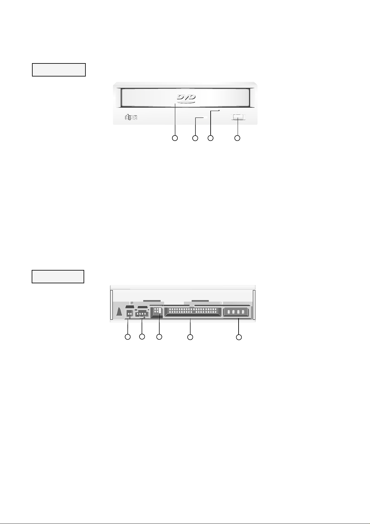
LOCATION OF CUSTOMER CONTROLS
(1) Digital Audio Output Connector
This connector is not supported.
(2) Analog Audio Output Connector
The Audio Output Connector connects to a sound
card.
(3) Master/Slave/CSEL Jumper
These three jumpers are used to set the DVD-ROM
Drive to either a Master, Slave, or CSEL device.
(4) Interface Connector
This 40-pin connector is used to transfer data and
control signals between the DVD-ROM Drive and your
PC.
(5) Power-in Connector
Attach a power cable from the computer to this
connector.
ROM
ROM
ROM
ROM
COMPACT
1
2
43
1
2
5
4
3
FRONT VIEW
BACK VIEW
(1) Disc Drawer
Accepts a CD-ROM/DVD-ROM disc on its tray.
(2) Busy Indicator
The Busy Indicator lights during initialization and dataread operations.
(3) Emergency Eject Hole
Insert a paper clip here to eject the drawer manually or
when there is no power.
(4) Open/Close/Stop Button
This button is pressed to open or close the CD tray.
If an audio CD is playing, pressing this button will stop
it, and pressing it
again will open the tray.
6
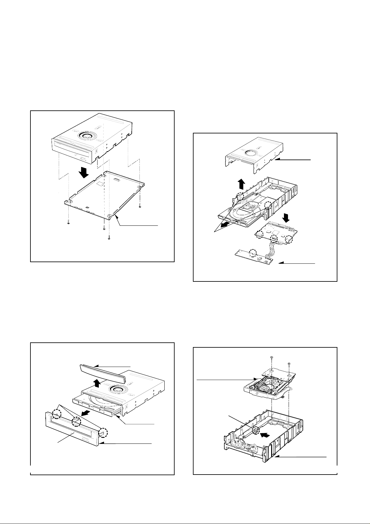
1. CABINET and CIRCUIT BOARD
DISASSEMBLY
1-1. Bottom Chassis
A. Release 4 screws (A) and remove the Bottom
Chassis in the direction of arrow (1). (See Fig. 1-1)
1-2. Front Bezel Assy
A. Insert and Press a rod in the Emergency Eject
Hole and then the CD Tray will open in the
direction of arrow (2).
B. Remove the Tray Door in the direction of arrow (3)
by pushing it outward.
C. Release 3 stoppers and remove the Front Bezel
Assy.
1-3. Cabinet and Main Circuit Board
A. Remove the Cabinet in the direction of arrow (4).
(See Fig. 1-3)
B. Release 2 hooks (a) and remove the CD Tray.
C. Remove the Soldering of the LD- and LD+ (B) for
the Loading Motor, and then remove the Main
Circuit Board.
D. At this time, be careful not to damage the 3
connectors of the Main Circuit Board.
2. MECHANISM ASSY
2-1. Base Pick-Unit Assy
A. Separate the Base Pick-Up Unit Assy from the
MechanismAssy.
B. Release 2 screws (C) and 1hook and then
remove the Base Pick-Up Unit Assy.
DISASSEMBLY
(A)
(A)
(A)
(A)
(1)
Bottom Chassis
Fig. 1-1
Fig. 1-2
Fig. 1-3
Fig. 2-1
Cabinet
(4)
Hooks (a)
(B)
Main
Circuit Board
Tray Door
(3)
Stoppers
Emergency Eject Hole
(2)
Front Bezel Assy
CD Tray
Base Pick-up Unit Assy
Hook
(C)
(C)
Mechanism Assy
PBM00 (MAIN C.B.A)
007
002
003
030
020
A02
A01
A03
020
051
028
050
029
434
021
434
434
413
413
413
001
413
430
028
027
026
025
024
435
033
434
010
009
008
011
012
005
034
013
434
017
016
015
004
006
022
021
430
A B C D E F GH
1
2
3
4
5
014
7 8
EXPLODED VIEW
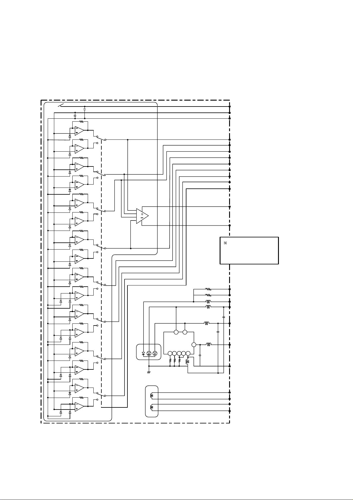
INTERNAL STRUCTURE OF THE PICK-UP
1.Structure of the Pick-Up
13
PICK-UP UNIT
Q001
CN18 VCC
CN06 VC (Vref).
CN05 GND-PD
CN10 A/a
CN09 B/b
CN15 C/c
CN14 D/d
CN17 E1/e2+f2
CN16 E2/e3+f3
CN07 F1/e1+f1
CN08 F2/e4+f4
CN11 CD/DVD SW
CN13 RF+
CN12 RF-
CN19 VR~CD
VR02
VR01
L003
L002
L001
L004
L005
R001
R002
R003
C003
C002
C001
42
1
35678
CN20 VR~DVD
CN22 MD
CN21 LD~CD
CN25 LD~DVD
CN23 HFM
CN26 GND-LD
CN01 F+
CN02 F-
CN03 T+
CN04 T-
Alphabet
A~D, E1, E2, F1, F2 -> CD
a~d, e1~ e4, f1~ f4 -> DVD
HFM
DVD= 0V
C D=+5V
Q002
A
a
B
b
C
c
D
d
E1
f2e2
E2
f3e3
F1
f1e1
F2
f4
ACTUATOR
Two wavelength
Laser diode
FOCUS
TRACKING
e4
14
For CD For DVD
SF-HD67
P/U
PCB
IC101
IC201
FFC
MD
CD
CD: Hi
DVD: Lo
Q102,Q104
VRCD VRDVD
222019
22
2 4
2019
175
Monitor resister SW circuit
1. Structure of the Pick-up
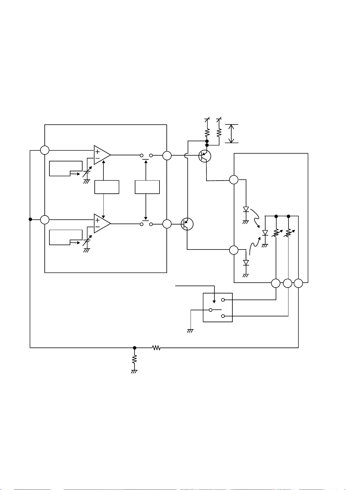
SF-HD67 is consist of monitor diode for DVD laser and CD laser.
When DVD laser is ON, CN101 20 Pin is need to connect GND for getting monitor voltage.(CN101 22 pin).
When CD laser is ON, CN101 19 Pin is need to connect GND for getting monitor voltage.(CN101 22 pin).
This control is done by handling Q102,Q104 from CD signal (IC201 175 pin output).
15
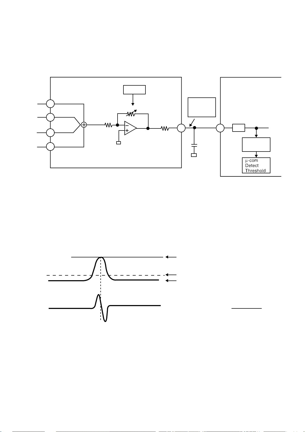
1) Focus Error Signal –> (A + C) - (B+C)
• In case of CD Disc
This signal is generated in RF AMP IC (IC101) and controls the pick-up’s up and down to
focus on CD Disc.
2) Tracking Error Signal (DPP( Differential Push Pull) )-> {(A+B) - (C+D)} - 1.9 x
{(E
1+F1) - (E2+F2)}
• In case of CD Disc
This signal is generated in RF AMP IC (IC101) and controls the pick-up’s left and right shift to
find the track on CD Disc.
3) RF Signal –> A+B+C+D
• In case of CD Disc
This signal is converted to DATA signal in DSP IC (IC201).
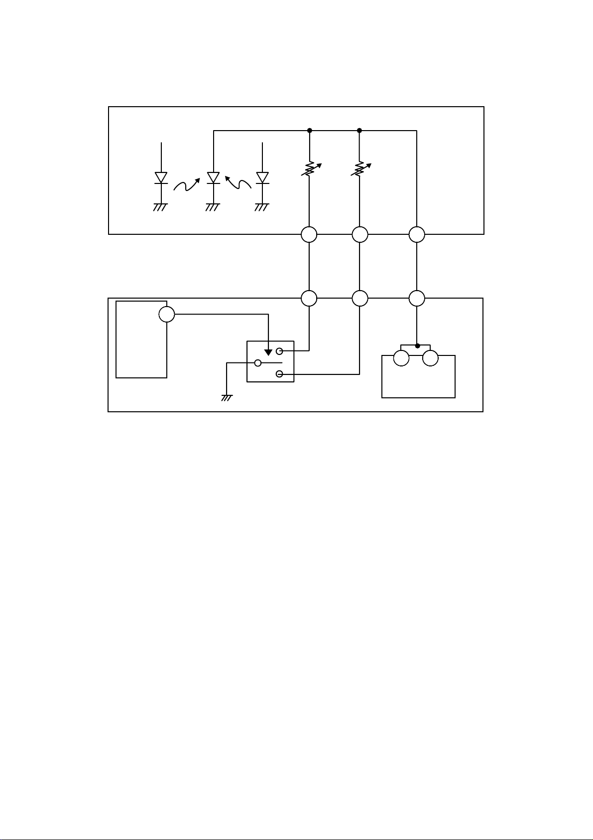
2.Structure of the Photo Diode (CD)
Infrared laser
Pick-Up module
Photo Diode
Tracking
Focusing
(As seen from light receiving side)
E2 E1
F2 F1
C
B
D
A
16
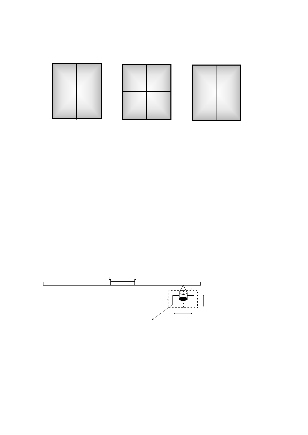
1) Focus Error Signal –> (a+c) - (b+d)
• In case of DVD Disc
This signal is generated in RF AMP IC (IC101) and controls the pick-up’s up and down to
focus on DVD Disc.
2) Tracking Error Signal (DPD Method) –> Differential phase of A and B + Differential
phase of C and D
• In case of DVD Disc
This signal is generated in RF AMP IC (IC101) and controls the pick-up’s left and right shift to find the track
on DVD Disc.
3) RF Signal –> (a+b+c+d)
• In case of DVD Disc
This signal is converted to DATA signal in DSP IC (IC201).
3.Structure of the Photo Diode (DVD-ROM)
(As seen from light
receiving side)
Red laser
Pick-Up module
Photo Diode
Tracking
Focusing
d
a
c
b
17
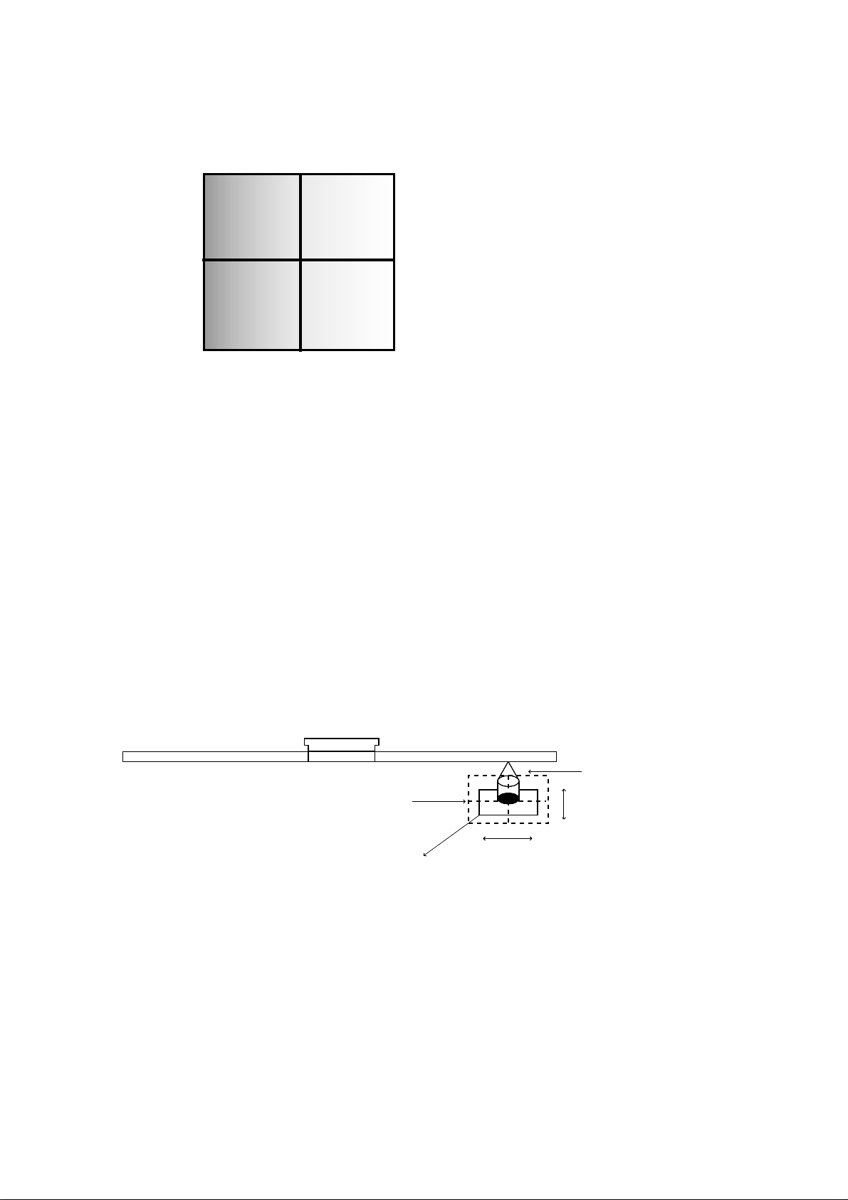
1) Focus Error Signal –> {(a+c) - (b+d)} - 1.17 x {(e2 + f2 + e4 + f4) - (e1 + f1 - e3 + f3)}
• In case of DVD Disc
This signal is generated in RF AMP IC (IC101) and controls the pick-up’s up and down to
focus on DVD Disc.
2) Tracking Error Signal (DPP Method) –> {(a+b) -(c+d)} - 1.17 x {(e1 + f1 + e2 + f2)
- (e
3 + f3 + e4 + f4)}
• In case of DVD Disc
This signal is generated in RF AMP IC (IC101) and controls the pick-up’s left and right shift to find the track
on DVD Disc.
3) RF Signal –> A+B+C+D
• In case of DVD Disc
This signal is converted to DATA signal in DSP IC (IC201).
4.Structure of the Photo Diode (DVD-RAM)
(As seen from light receiving side)
Red laser
Pick-Up module
Photo Diode
Tracking
Focusing
d
a
c
b
e4
e1
e3
e2
f4
f1
f3
f2
18
3
5
4
2
25
21
19 20 22
Q102,
Q110
Q110
IC101
P/U
5V
For DVD
For CD
LDOFF
LDSEL
LDPWR0.1
LDRWR0.1
MD
MD
DVD-RAM 4.7G : about 0.77V
DVD-RAM 2.6G : about 0.68V
DVD-ROM : about 0.68V
CD : about 0.7V
CD
Q104
DESCRIPTION OF CIRCUIT
1. ALPC (Automatic laser power control)
1-1. ALPC Circuit Constitution
Dual laser power control for DVD and CD are provided.
The laser ON for DVD or CD can be selected by ¡ LDSEL¡–and the lasers ON/OFF are controlled by ¡ LDOFF¡–.
Laser power for DVD and CD can be programmable by ¡ LDPWR 0,1¡–
ALPC (Automatic laser plower control)
DVD-RAM 4.7G : about 0.23V
DVD-RAM 2.6G : about 0.18V
DVD-ROM : about 0.18V
CD : about 0.19V
19
x1
EQVGA
BST
x1
2
34
35
13
IC201
IC101
For boost
0.5Vpp
ARF
NARF
0.5Vpp
Slicer
PLL
PWM
For fc
1.65V
RFINN
RFINP
AGCG AGCO
81
99
9824
23
31 32
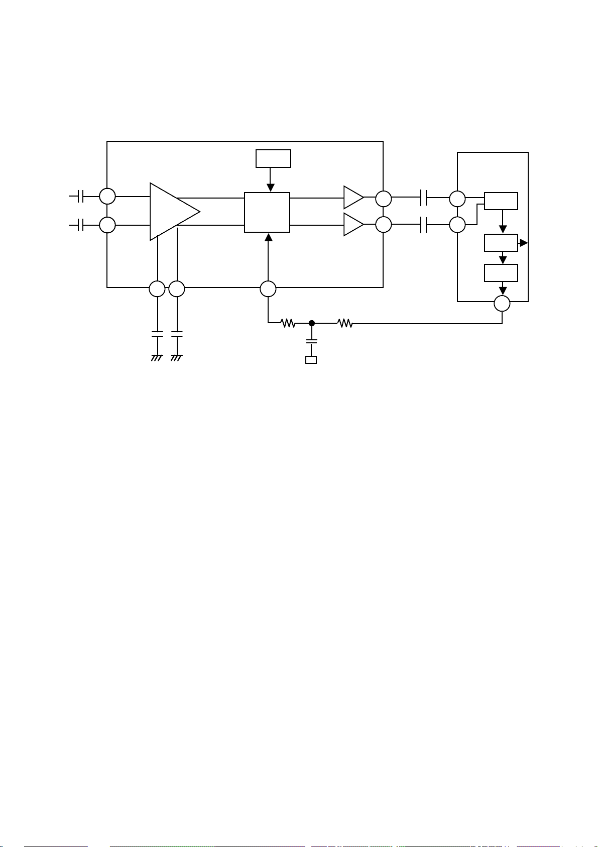
2. RF Amplifier Circuit
RF Amplifier Circuit
2-1. Input stage
The differential RF signal for data read from pick up may feed into IC101 pin 34 and pin 35.
2-2. AGC (Automatic Gain Control) Loop
This RF signal is controlled to 0.5 Vpp in VGA.
The capacitor which is connected in 31 pin is used to control constant level of amplitude.
The capacitor which is connected in 32 pin is used to control DC offset of RF signal.
2-3. Equalizer
EQ boost gain is controlled by u-com and register ¡ BST¡–.
Fc of EQ is linear by real velocity and feed into IC101 13pin and changed by current differentially.
20
FESEL 0, 1
Offset Add.
circuit
FEG
1.65V
FE
3.3V
1.65V
FBAL
x1.17
x1
x1
x1
7
44
46
47
43
40
39
37
36
Detect
Amplitude
A/D
PWM
PLL
57
10918
106
IC201
S-Curve : about 1.65Vpp
S-Center : 1.65V
F1
F2
E2
E1
A
B
C
D
DA
Tracking
BC
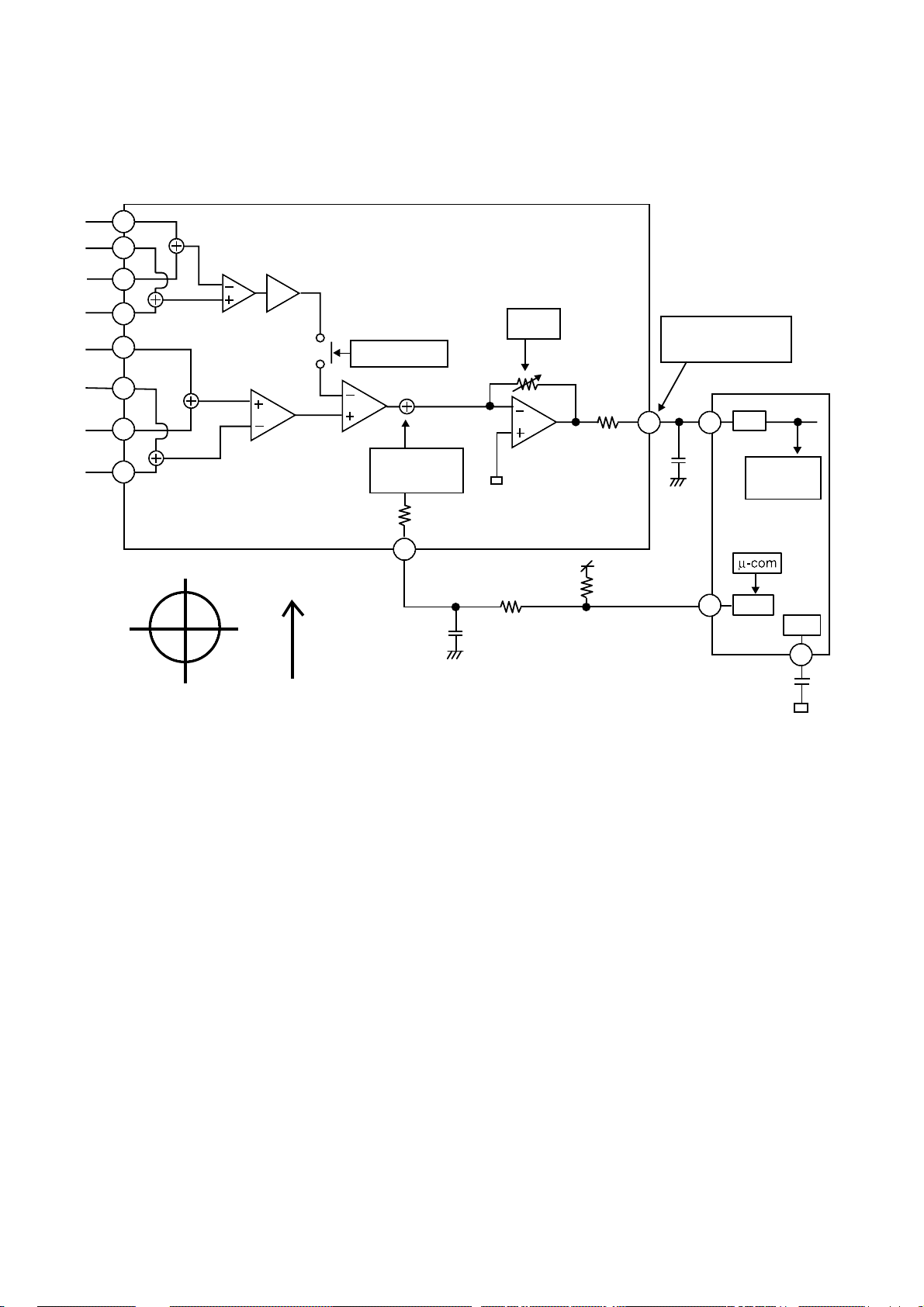
3. SERVO SIGNAL
3-1. FOCUSING ERROR (FE)
Focusing Error circuit
FE for DVD-ROM,CD are made from 4D(A,B,C,D).
FE S-curve amplitude is detected from IC201 109 pin and FE gain is controlled by register “FEG” to keep 1.65V
amplitude.
Center Voltage of FE is about 1.65V.
Offset adjustment for added FE keep max voltage with jitter min.
Added offset quantity is programmable by current which feed into IC101 7 pin from IC201 57 pin.
FE for DVD-RAM 2.6G,4.7G is obtained from 4D(A,B,C,D) or sub spot(Sub beam) (E1,E2,F1,F2).
For DVD-RAM 2.6G, 4.7G, offset is occurred when track is crossed.
The reason for sub spot(sub beam) add is cancel of offset.
21
3-2. AS (ALL SUM)
ASG
47
46
44
43
A
D
C
B
IC101 IC201
1.65V
1.65V
V
2 (V)
threshold (V)
V
1 (V)
A/D
AS
Detect
Amplitude
FOCUS ON
: about 2.5V
FOCUS OFF
: about 1.65V
11016
AS
FE
Threshold(V) = V1(V) +
V2(V) - V1(V)
8
AS circuit
AS(All sum) signal is obtained from low pass filter and FOK is made from AS signal in IC201.
This FOK signal is used to check servo status.
Threshold is that compare with AS signal to obtain FOK signal.
Threshold can be made to focus sweep(Training) in initial read.
22
1.65V
1.65V
Balance
Detect
PWM
111
IC201
DPD
DPD
EQ
EQ
EQ
EQ
H.P.F
H.P.F.
H.P.F
H.P.F.
TESEL
DPP
TEG
14
TE
1.65Vpp
Center Voltage = 1.65V
A/D
43
44
46
47
A
D
C
B
3-3. TRACKING ERROR (TE)
3-3-1. TE for DVD-ROM (DPD)
Tracking error Circuit
TE signal for DVD-ROM is made by DPD (Differential Phase Detect) method.
TE signal is made that add voltage obtain form phase differnece of front spot A, D to voltage obtain two phase
difference of rear spot B, C.
Final stage amp gain is determined by register “TEG” and TE signal amplitude is about 1.65Vpp. (Center
voltage of TE signal is about 1.65V)
Balance of TE signal center voltage is 1.65V.
Adjustment is operated by monitoring TE signal balance which feed into IC201 111pin.
 Loading...