

LG GD880 Service Manual
Service Manual Model : GD880
Internal Use Only
Service Manual
GD880
Date: March, 2010 / Issue 1.0

Table Of Contents
1. INTRODUCTION ................................................. 5
1.1 Purpose ............................................................................................... 5
1.2 Regulatory Information ............................................................... 5
1.3 Abbreviations ................................................................................... 7
2. PERFORMANCE ..................................................9
2.1 Product Name .................................................................................. 9
2.2 Supporting Standard .................................................................... 9
2.3 Main Parts : GSM Solution ........................................................... 9
2.4HW Features .....................................................................................10
2.5SW Features .....................................................................................12
2.6 HW SPEC. ..........................................................................................14
2.7 GD880 Figures ...............................................................................20
3. TECHNICAL BRIEF ............................................21
3.1 Digital Baseband(DBB/MSM7227) .........................................21
3.2 Hardware Architecture ..............................................................22
3.3 Sub system(MSM7227)...............................................................25
3.4 Power Block.....................................................................................34
3.5 External memory interface .......................................................39
3.6 H/W Sub system ............................................................................41
3.7 Audio and sound ..........................................................................52
3.8 Camera / LCD ..................................................................................58
3.9 Proximity Sensor ...........................................................................65
3.10 Luminance Sensor .....................................................................66
3.11 Motion Sensor .............................................................................67
3.12 Vibrators .........................................................................................68
3.13 GSM MODE ...................................................................................70
3.14 UMTS MODE .................................................................................72
3.15 GPS RECEIVER ..............................................................................75
3.16 LO GENERATION and DISTRIBUTION CIRCUIT ................75
3.17 OFF-CHIP RF COMPONENTS ..................................................76
3.18 LG GD880 Main Features.........................................................80
3.19 GD880 Main Component .......................................................81
4. TROUBLE SHOOTING ......................................86
4.1 RF Component...............................................................................86
4.2 Signal Path .......................................................................................88
4.3 Checking TCXO Block ..................................................................92
4.4 Checking FEM Block ....................................................................93
4.5 Checking WCDMA Block ............................................................96
4.6 Checking GSM Block ................................................................ 106
4.7 GPS/WIFI/BT/FM Radio RF components .......................... 113
4.8 GPS/WIFI/BT/FM Radio SIGNAL PATH ................................115
4.9 GPS/WIFI/BT/FM Radio TROUBLE SHOOTING ................116
4.10 Power ON Troubleshooting ................................................ 122
4.11 Charger Troubleshooting .................................................... 126
4.12 USB trouble................................................................................ 130
4.13 Audio trouble ...........................................................................133
4. 14 5M Camera trouble ............................................................... 145
4. 15 VGA Camera trouble ............................................................. 148
4. 16 Main LCD trouble ................................................................... 150
4.17 SIM Detect Troubleshooting ..............................................153
4.18 Side Key Troubleshooting.................................................... 155
4.19 LINEAR MOTOR ........................................................................157
4.20 Proximity Sensor on/off trouble ....................................... 158
4.21 Luminance Sensor on/off trouble ....................................160
4.22 Motion Sensor on/off trouble ............................................162
5. DOWNLOAD ...................................................164
6. BLOCK DIAGRAM ...........................................177
7. CIRCUIT DIAGRAM ........................................185
8. BGA PIN MAP .................................................195
9. PCB LAYOUT ...................................................201
10. RF CALIBRATION .........................................205
10.1 Introduction .............................................................................. 206
10.2 Terminology ..............................................................................206
10.3 Tachyon Main UI ......................................................................206
11. EXPLODED VIEW & REPLACEMENT
PART LIST ....................................................215
11.1 EXPLODED VIEW ......................................................................215
11.2 Replacement Parts..................................................................219
11.3 Accessory ...................................................................................244
Copyright © 2010 LG Electronics. Inc. All right reserved.
Only for training and service purposes
- 3 -
LGE Internal Use Only

LGE Internal Use Only Copyright © 2010 LG Electronics. Inc. All right reserved.
- 4 -
Only for training and service purposes

1. INTRODUCTION
1.1 Purpose
This manual provides the information necessary to repair, calibration, description and download the
features of this model.
1.2 Regulatory Information
A. Security
Toll fraud, the unauthorized use of telecommunications system by an unauthorized part (for example,
persons other than your company’s employees, agents, subcontractors, or person working on your
company’s behalf) can result in substantial additional charges for your telecommunications services.
System users are responsible for the security of own system. There are may be risks of toll fraud associated
with your telecommunications system. System users are responsible for programming and configuring the
equipment to prevent unauthorized use. The manufacturer does not warrant that this product is immune
from the above case but will prevent unauthorized use of common-carrier telecommunication service of
facilities accessed through or connected to it.
The manufacturer will not be responsible for any charges that result from such unauthorized use.
B. Incidence of Harm
If a telephone company determines that the equipment provided to customer is faulty and possibly
causing harm or interruption in service to the telephone network, it should disconnect telephone service
until repair can be done. A telephone company may temporarily disconnect service as long as repair is not
done.
C. Changes in Service
A local telephone company may make changes in its communications facilities or procedure. If these
changes could reasonably be expected to affect the use of the this phone or compatibility with the
network, the telephone company is required to give advanced written notice to the user, allowing the user
to take appropriate steps to maintain telephone service.
D. Maintenance Limitations
Maintenance limitations on this model must be performed only by the manufacturer or its authorized
agent. The user may not make any changes and/or repairs expect as specifically noted in this manual.
Therefore, note that unauthorized alternations or repair may affect the regulatory status of the system and
may void any remaining warranty.
1. INTRODUCTION
1. INTRODUCTION
Copyright © 2010 LG Electronics. Inc. All right reserved.
Only for training and service purposes
- 5 -
LGE Internal Use Only

1. INTRODUCTION
E. Notice of Radiated Emissions
This model complies with rules regarding radiation and radio frequency emission as defined by local
regulatory agencies. In accordance with these agencies, you may be required to provide information such
as the following to the end user.
F. Pictures
The pictures in this manual are for illustrative purposes only; your actual hardware may look slightly
different.
G. Interference and Attenuation
Phone may interfere with sensitive laboratory equipment, medical equipment, etc.Interference from
unsuppressed engines or electric motors may cause problems.
H. Electrostatic Sensitive Devices
ATTENTION
Boards, which contain Electrostatic Sensitive Device (ESD), are indicated
by the sign. Following information is ESD handling:
• Service personnel should ground themselves by using a wrist strap when exchange system boards.
• When repairs are made to a system board, they should spread the floor with anti-static mat
which is also grounded.
• Use a suitable, grounded soldering iron.
• Keep sensitive parts in these protective packages until these are used.
• When returning system boards or parts like EEPROM to the factory, use the protective
package as described.
2. INTRODUCTION
LGE Internal Use Only Copyright © 2010 LG Electronics. Inc. All right reserved.
- 6 -
Only for training and service purposes
1.3 Abbreviations
For the purposes of this manual, following abbreviations apply:
Offset Phase Locked LoopOPLL
Light Emitting DiodeLED
Low Drop OutputLDO
Liquid Crystal DisplayLCD
Intermediate FrequencyIF
International Portable User IdentityIPUI
Global System for Mobile CommunicationsGSM
General Purpose Interface BusGPIB
Gaussian Minimum Shift KeyingGMSK
Flexible Printed Circuit BoardFPCB
Electrostatic DischargeESD
Electrical Erasable Programmable Read-Only MemoryEEPROM
Digital Signal ProcessingDSP
dB relative to 1 milli wattdBm
Digital Communication SystemDCS
Digital to Analog ConverterDAC
Constant Current – Constant VoltageCC-CV
Bit Error RatioBER
BasebandBB
Automatic Power ControlAPC
1. INTRODUCTION
1. INTRODUCTION
Copyright © 2010 LG Electronics. Inc. All right reserved.
Only for training and service purposes
- 7 -
LGE Internal Use Only
1. INTRODUCTION
Wireless Application Protocol
WAP
Voltage Control Temperature Compensated Crystal OscillatorVCTCXO
Voltage Controlled OscillatorVCO
Universal Asynchronous Receiver/TransmitterUART
Time Division Multiple AccessTDMA
Time Division DuplexTDD
Travel AdapterTA
Side Tone Masking RatingSTMR
Pseudo SRAMPSRAM
Static Random Access MemorySRAM
Sending Loudness RatingSLR
Subscriber Identity ModuleSIM
Surface Acoustic WaveSAW
Real Time ClockRTC
Root Mean SquareRMS
Receiving Loudness RatingRLR
Radio FrequencyRF
Public Switched Telephone NetworkPSTN
Phase Locked LoopPLL
Programmable Gain AmplifierPGA
Printed Circuit BoardPCB
Power Amplifier ModulePAM
1. INTRODUCTION
LGE Internal Use Only Copyright © 2010 LG Electronics. Inc. All right reserved.
- 8 -
Only for training and service purposes

2. PERFORMANCE
GD880 Product SPEC
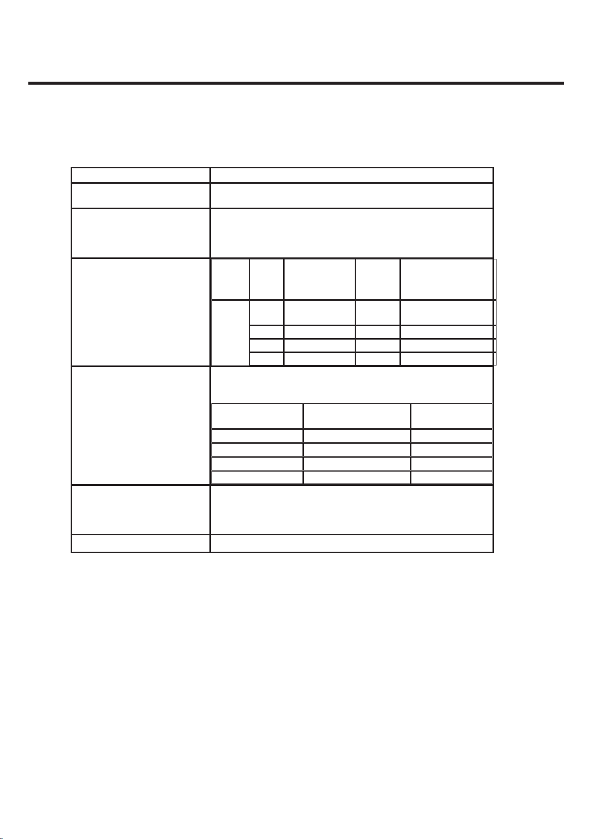
2.1 Product Name
GD880 : WCDMA900/2100+EGSM/GSM850/DCS/PCS
(HSDPA 7.2Mbps / GPRS Class 12 / EDGE Class 12)
2.2 Supporting Standard
Item Feature Comment
Supporting Standard WCDMA(FDD1,8)/EGSM/GSM850/DCS1800/PCS1900
with seamless handover
Phase 2+(include AMR)
SIM Toolkit: Class 1, 2, 3, C-E
Frequency Range WCDMA(FDD1) TX : 1920 – 1980 MHz
WCDMA(FDD1) RX : 2110 – 2170 MHz
WCDMA(FDD8) TX : 880 – 915 MHz
WCDMA(FDD8) RX : 925 – 960 MHz
EGSM TX: 880 – 915 MHz
EGSM RX: 925 – 960 MHz
GSM850 TX: 824 – 849 MHz
GSM850 RX: 869 – 894 MHz
DCS1800 TX : 1710 – 1785 MHz
DCS1800 RX: 1805 – 1880 MHz
PCS1900 TX: 1850 – 1910 MHz
PCS1900 RX: 1930 – 1990 MHz
Application Standard WAP 2.0, JAVA 2.0
2.3 Main Parts : GSM Solution
Item Part Name Comment
Digital Baseband MSM7227 : Qualcomm
Analog Baseband PM7540 : Qualcomm
RF Chip RTR6285 : Qualcomm
2. PERFORMANCE
Copyright © 2010 LG Electronics. Inc. All right reserved.
Only for training and service purposes
- 9 -
LGE Internal Use Only
2. PERFORMANCE
GD880 Product SPEC
2.4HW Features
Item Feature Comment
Form Factor Bar type
Battery 1) Capacity
Standard : Li-Ion, 900mAh
2) Packing Type : Soft Pack
Size Standard :
102 x 47.6 x 10.6 mm
Weight 99g With Battery
Volume
T
BD
PCB All Layer (10) , 0.75t
Stand by time 2G Up to 340 hrs
3G Up to 300 hrs
@ Paging Period 5 (2G)
@ DRX 7 (3G)
Charging time 3 hrs @ Power Off / 900mAh
T
alk time 2G Up to 190mins
3G Up to 250 mins
@ Power Level 5 (2G)
@ Tx = 12dBm (3G)
RX sensitivity WCDMA(FDD1) : -106.7 dBm
WCDMA(FDD8) : -103.7 dBm
EGSM : -105 dBm
GSM850 : -105 dBm
DCS 1800 : -105 dBm
PCS 1900 : -105 dBm
T
X
output
power
WCDMA/
GSM/
GPRS
WCDMA : 24dBm/3.84MHz,+1/-3dBm
EGSM : 33dBm
GSM850 : 33 dBm
DCS 1800 : 30 dBm
PCS 1900 : 30 dBm
Class3(WCDMA)
Class4 (EGSM)
Class4 (GSM850)
Class1 (PCS)
Class1 (DCS)
EDGE GSM 900 : 27 dBm
DCS 1800 : 26 dBm
PCS 1900 : 26 dBm
E2 (GSM900)
E2 (PCS)
E2 (DCS)
GPRS compatibility GPRS Class 12
EDGE compatibility EDGE Class 12
SIM card type Plug-In SIM
3V /1.8V
Display Main LCD
TFT Main LCD(3.2’, 480 x 854)
Built-in Camera
5M CMOS Camera
1.3M CMOS Camera (VGA)
Status Indicator Yes
Keypad Function Key : 2
Side Key : 2
Function Key:
CAM, Power
Side Key :
Volume up/down
1.3M VGA CMOS Camera
No
No
320 hrs
180 mins
225 mins
LGE Internal Use Only Copyright © 2010 LG Electronics. Inc. All right reserved.
- 10 -
Only for training and service purposes
2. PERFORMANCE
GD880 Product SPEC
ANT Main : Internal Fixed Type
System connector 5 Pin
Ear Phone Jack 3.5Phi, 4 Pole, Stereo
PC synchronization Yes
Memory NAND Flash : 4Gbit
SDRAM : 4Gbit
Speech coding FR, EFR, HR,AMR
Data & Fax Built in Data & Fax support
Vibrator Built in Vibrator
Blue Tooth V2.1+ EDR
MIDI(for Buzzer
Function)
SW Decoded 72Poly
Music Player MP3/AAC/AAC+
Video Player MPEG4, H.263,
Camcorder MPEG4, H.263,
Voice Recording Yes
Speaker Phone mode
Support
Yes
T
ravel Adapter Yes
CDROM Yes
Stereo Headset Yes
Data Cable Yes
T
-Flash
(External Memory)
Yes
Copyright © 2010 LG Electronics. Inc. All right reserved.
Only for training and service purposes
- 11 -
LGE Internal Use Only
2. PERFORMANCE
GD880 Product SPEC
2.5SW Features
Item Feature Comment
RSSI 0 ~ 7 Levels
Battery Charging 0 ~ 3 Levels
Key Volume 0 ~ 7 Level
Audio Volume 1 ~ 20 Level
T
ime / Date Display Yes
Multi-Language Yes English/Spanish/Portuguese
/K
orean
Quick Access Mode Dialing / Call Log / Contact / Menu/
Message / Camera / Favorite
PC Sync Schedule / Phonebook / MEMO / SMS /
Download (Photo, file)
Speed Dial Yes (1~9) Voice mail center -> 1 key
Profile Yes
CLIP / CLIR Yes
Phone Book Name + 5 Numbers + 1 Memo + 2 e-mail
+ 3 Group Select + Picture + Ringtone +
Anniversary day
T
otal 1000 Member
Last Dial Number Yes
T
otal Call DB Max 100
LDN (SIM) N/A
Last Received
Number
Yes
T
otal Call DB Max 100
LDN (SIM) N/A
Last Missed Number Yes
T
otal Call DB Max 100
LDN (SIM) N/A
Search by Number
/ Name
Name and Number
Group 30
Fixed Dial Number Yes
Service Dial Number Yes
Own Number Yes
Voice Memo Yes
Call Reminder Yes
Network Selection Automatic
Mute Yes
Call Divert Yes
Call Barring Yes
Call Charge (AoC) Yes
Call Duration Yes
SMS (EMS) 1000 (10) EMS : Release4
(Except Text align)
SMS Over GPRS Yes
EMS Melody / Picture
Send / Receive / Save
Yes
Receive only
MMS MPEG4
Send / Receive / Save
Yes
Yes
LGE Internal Use Only Copyright © 2010 LG Electronics. Inc. All right reserved.
- 12 -
Only for training and service purposes
GD880 Product SPEC
Long Message MAX 1000 Characters SMS 7pages
Cell Broadcast Yes
Download Over the WAP
Game Yes
Calendar Yes
Memo 50
World Clock Yes
Unit Convert Currency/Surface/Length/Volume/Weig
ht/Temperature/Velocity
Stop Watch Yes
Wall Paper Yes
WAP Browser Over WAP 2.0 Obigo
Download Melody /
Wallpaper
Yes Over WAP
SIM Lock Yes Operator Dependent
SIM Toolkit Class 1, 2, 3, C-E
MMS Yes Obigo +LG MMS Client
EONS Yes
CPHS Yes V4.2
ENS No
Camera Yes 5M AF/
Digital Zoom : x16
JAVA Yes CLDC V1.1 / MIDP V2.0
Download Over WAP
Voice Dial No
IrDa No
Bluetooth Yes V2.0
HSP, HFP, OPP, FTP(server), BPP,
A2DP, AVRCP
FM radio Yes
GPRS Yes Class 12
EDGE Yes Class 12
Hold / Retrieve Yes
Conference Call Yes Max. 6
DTMF Yes
Memo pad Yes
T
TY No
AMR Yes
SyncML Yes
IM No
Email Yes
2. PERFORMANCE
Copyright © 2010 LG Electronics. Inc. All right reserved.
Only for training and service purposes
- 13 -
LGE Internal Use Only
2. PERFORMANCE
GD880 Product SPEC
2.6 HW SPEC.
1) GSM transceiver specification
Item Specification
Phase Error
Rms : 5°
Peak : 20 °
Frequency Error
GSM : 0.1 ppm
DCS/PCS : 0.1 ppm
EMC(Radiated Spurious
Emission Disturbance)
GSM/DCS : < -28dBm
T
ransmitter Output power and
Burst Timing
GSM : 5dBm – 33dBm ± 3dB
DCS/PCS : 0dBm – 30dBm ± 3dB
Burst Timing <3.69us
Spectrum due to modulation out
to less than 1800kHz offset
200kHz : -36dBm
600kHz : -51dBm/-56dBm
Spectrum due to modulation out
to larger than 1800kHz offset to
the edge of the transmit band
GSM :
1800-3000kHz :< -63dBc(-46dBm)
3000kHz-6000kHz : <-65dBc(-46dBm)
6000kHz < : < -71dBc(-46dBm)
DCS :
1800-3000kHz :< -65dBc(-51dBm)
6000kHz < : < -73dBc(-51dBm)
Spectrum due to switching transient
400kHz : -19dBm/-22dBm(5/0), -23dBm
600kHz : -21dBm/-24dBm(5/0), -26dBm
Reference Sensitivity – TCH/FS Class II(RBER) : -105dBm(2.439%)
Usable receiver input level range 0.012(-15 - -40dBm)
Intermodulation rejection –
Speech channels
± 800kHz, ± 1600kHz
: -98dBm/-96dBm (2.439%)
AM Suppression
T GSM : -31dBm
- DCS : -29dBm
-98dBm/-96dBm (2.439%)
T
iming Advance ± 0.5
T
LGE Internal Use Only Copyright © 2010 LG Electronics. Inc. All right reserved.
- 14 -
Only for training and service purposes
GD880 Product SPEC
2) WCDMA transmitter specification
Item Specification
T
ransmit Frequency Band1 : 1920 MHz ~ 1980 MHz
Band8 : 880MHz~915MHz
Maximum Output Power +24 dBm / 3.84 MHz, +1 / -3 dB
Frequency Error within ±0.1 PPM
Open Loop Power Control Normal Conditions : within ±9 dB,
Extreme Conditions : within ±12 dB
Minimum Transmit Power < -50 dBm /3.84 MHz
Occupied Bandwidth < 5 MHz at 3.84 Mcps (99% of power)
Adjacent Channel Leakage
Power Ratio (ACLR)
> 33 dB @ ±5 MHz,
> 43 dB @ ±10 MHz
Spurious Emissions
|f-fc| > 12.5 MHz
< -36 dBm / 1 kHz RW @ 9 kHz ≤ f < 150 kHz
< -36 dBm / 10 kHz RW @ 150 KHz ≤ f < 30 MHz
< -36 dBm / 100 kHz RW @ 30 MHz ≤ f < 1 GHz
< -30 dBm / 1 MHz RW @ 1 GHz ≤ f < 12.75 GHz
< -60 dBm / 3.84 MHz RW @ 869 MHz ≤ f ≤ 894 MHz
< -60 dBm / 3.84 MHz RW @ 1930 MHz ≤ f ≤ 1900 MHz
< -60 dBm / 3.84 MHz RW @ 2110 MHz ≤ f ≤ 2155 MHz
< -67 dBm / 100 kHz RW @ 925 MHz ≤ f ≤ 935 MHz
< -79 dBm / 100 kHz RW @ 935 MHz < f ≤ 960 GHz
< -71 dBm / 100 kHz RW @ 1805 MHz ≤ f ≤ 1880 MHz
< -41 dBm / 300 kHz RW @ 1884.5 MHz < f < 1919.6 MHz
T
ransmit Intermodulation < -31 dBc @ 5 MHz & < -41 dBc @ 10 MHz
when Interference CW Signal Level = -40 dBc
Error Vector Magnitude < 17.5 %, when Pout ≥ -20 dBm
Peak Code Domain Error
< -15 dB at Pout t -20 dBm
2. PERFORMANCE
Copyright © 2010 LG Electronics. Inc. All right reserved.
Only for training and service purposes
- 15 -
LGE Internal Use Only
2. PERFORMANCE
GD880 Product SPEC
3) WCDMA receiver specification
Item Specification
Receive Frequency Band1 : 2110 ~ 2170 MHz
Band8 : 925~960MHz
Reference Sensitivity Level Band1 : BER < 0.001 when Îor = -106.7 dBm / 3.84 MHz
Band8 : BER < 0.001 when Îor = -103.7 dBm / 3.84 MHz
Maximum Input Level BER < 0.001 when Îor = -25 dBm / 3.84 MHz
Adjacent Channel Selectivity
(ACS)
ACS > 33 dB where BER < 0.001 when
Îor = -92.7 dBm / 3.84 MHz
& Ioac = –52 dBm / 3.84 MHz @ ±5 MHz
Blocking Characteristic BER < 0.001 when Îor = -103.7 dBm / 3.84 MHz
& Iblocking = -56 dBm / 3.84 MHz @ Fuw(offset) = ±10 MHz
or Iblocking = -44 dBm / 3.84 MHz @ Fuw(offset) = ±15 MHz
Spurious Response BER < 0.001 when Îor = -103.7 dBm / 3.84 MHz
& Iblocking = -44 dBm
Intermodulation BER < 0.001 when Îor= -103.7 dBm / 3.84 MHz
& Iouw1 = -46 dBm @ Fuw1(offset) = ±10 MHz
& Iouw2 = -46 dBm / 3.84 MHz @ Fuw2(offset) = ±20 MHz
Spurious Emissions < -57 dBm / 100 kHz BW @ 9 kHz ≤ f < 1 GHz
< -47 dBm / 1 MHz BW @ 1 GHz ≤ f ≤ 12.75 GHz
Inner Loop Power Control
In Uplink
Adjust output(TPC command)
cmd 1dB 2dB 3dB
+1 +0.5/1.5 +1/3 +1.5/4
0 -0.5/+0.5 -0.5/+0.5 -0.5/+0.5
-1 -0.5/-1.5 -1/-3 -1.5/-4
group(10equal command group)
+1 +8/+12 +16/+24
LGE Internal Use Only Copyright © 2010 LG Electronics. Inc. All right reserved.
- 16 -
Only for training and service purposes
2. PERFORMANCE
GD880 Product SPEC
4) HSDPA transmitter specification
Item Specification
T
ransmit Frequency Band1 : 1920 MHz ~ 1980 MHz
Band8 : 880MHz~915 MHz
Maximum Output Power Sub
-
T
est
1=1/15, 2=12/15 21~25dBm / 3.84 MHz
3=13/15 4=15/8 20~25dBm / 3.84 MHz
5=15/7 6=15/0 19~25dBm / 3.84 MHz
HS-DPCCH
Sub-test
in table
C.10.1.4
Power
step
Power step slot
boundary
Power
step size,
P [dB]
Transmitter power
step tolerance [dB]
5
1 Start of
Ack/Nack
6 +/- 2.3
2 Start of CQI 1 +/- 0.6
3 Middle of CQI 0 +/- 0.6
4 End of CQI 5 +/- 2.3
Spectrum Emission Mask
Sub-Test : 1=1/15, 2=12/15, 3=13/15, 4=15/8, 5=15/7, 6=15/0
Frequency offset
from carrier f
Minimum requirement
Measurement
Bandwidth
2.5 ~ 3.5 MHz
-35-15×(f-2.5)dBc
30 kHz
3.5 ~ 7.5 MHz
-35-1×(f-3.5)dBc
1 MHz
7.5 ~ 8.5 MHz
-35-10×(f-7.5)dBc
1 MHz
8.5 ~ 12.5 MHz -49dBc 1 MHz
Adjacent Channel Leakage
Power Ratio (ACLR)
Sub
-
T
est : 1=1/15, 2=12/15, 3=13/15, 4=15/8, 5=15/7, 6=15/0
> 33 dB @ ±5 MHz
> 43 dB @ ±10 MHz
Error Vector Magnitude < 17.5 %, when Pout ≥ -20 dBm
Copyright © 2010 LG Electronics. Inc. All right reserved.
Only for training and service purposes
- 17 -
LGE Internal Use Only
2. PERFORMANCE
GD880 Product SPEC
6) WLAN 802.11b transceiver specification
Item Specification
T
ransmit Frequency 2400 MHz ~ 2483.5 MHz ( CH1~CH13 )
T
x Power Level ≤ 20dBm under (Europe), ≤ 30dBm under (USA)
Frequency Tolerance within ±25 PPM
Chip clock Frequency
Tolerance
within ±25 PPM
Spectrum Mask ≤ -30 @ fc-22MHz< f <fc-11MHz and fc+11MHz< f <fc+22MHz
≤ -50 @ f < fc-22MHz and f > fc+22MHz
Power ramp on/off time ≤ 2us
Carrier Suppression ≤ -15dB
Modulation Accuracy
(Peak EVM)
≤ 35%
Spurious Emissions < -36 dBm @ 30MHz ~ 1GHz
< -30 dBm above @ 1GHz ~ 12.75GHz
< -47 dBm @ 1.8GHz ~ 1.9GHz
< -47 dBm @ 5.15GHz ~ 5.3GHz
Rx Min input Sensitivity ≤ -76dBm(1Mbps,2Mbps,5.5Mbps,11Mbps) @ FER ≤ 8%
Rx Max input Sensitivity ≥ -10dBm(1Mbps,2Mbps,5.5Mbps,11Mbps) @ FER ≤ 8%
Rx Adjacent Channel
Rejection
≥ 35dB @FER ≤ 8%,
interference input signal -70dBm@fc±25MHz(11Mbps)
GD880 Product SPEC
4) HSDPA transmitter specification
Item Specification
T
ransmit Frequency Band1 : 1920 MHz ~ 1980 MHz
Band8 : 880MHz~915 MHz
Maximum Output Power Sub
-
T
est
1=1/15, 2=12/15 21~25dBm / 3.84 MHz
3=13/15 4=15/8 20~25dBm / 3.84 MHz
5=15/7 6=15/0 19~25dBm / 3.84 MHz
HS-DPCCH
Sub-test
in table
C.10.1.4
Power
step
Power step slot
boundary
Power
step size,
P [dB]
Transmitter power
step tolerance [dB]
5
1 Start of
Ack/Nack
6 +/- 2.3
2 Start of CQI 1 +/- 0.6
3 Middle of CQI 0 +/- 0.6
4 End of CQI 5 +/- 2.3
Spectrum Emission Mask
Sub-Test : 1=1/15, 2=12/15, 3=13/15, 4=15/8, 5=15/7, 6=15/0
Frequency offset
from carrier f
Minimum requirement
Measurement
Bandwidth
2.5 ~ 3.5 MHz
-35-15×(f-2.5)dBc
30 kHz
3.5 ~ 7.5 MHz
-35-1×(f-3.5)dBc
1 MHz
7.5 ~ 8.5 MHz
-35-10×(f-7.5)dBc
1 MHz
8.5 ~ 12.5 MHz -49dBc 1 MHz
Adjacent Channel Leakage
Power Ratio (ACLR)
Sub
-
T
est : 1=1/15, 2=12/15, 3=13/15, 4=15/8, 5=15/7, 6=15/0
> 33 dB @ ±5 MHz
> 43 dB @ ±10 MHz
Error Vector Magnitude < 17.5 %, when Pout ≥ -20 dBm
5) HSDPA receiver specification
Item Specification
Receive Frequency
Band1 : 2110 ~ 2170 MHz
Band8 : 925 ~ 960Hz
Maximum Input Level
(BLER or R), 16QAM Only
Sub
-
T
est : 1=1/15, 2=12/15, 3=13/15, 4=15/8, 5=15/7, 6=15/0
BLER < 10% or R >= 700kbps
LGE Internal Use Only Copyright © 2010 LG Electronics. Inc. All right reserved.
- 18 -
Only for training and service purposes
GD880 Product SPEC
7) WLAN 802.11g transceiver specification
Item Specification
T
ransmit Frequency 2400 MHz ~ 2483.5 MHz ( CH1~CH13 )
T
x Power Level ≤ 20dBm under (Europe), ≤ 30dBm under (USA)
Frequency Tolerance within ±25 PPM
Chip clock Frequency
Tolerance
within ±25 PPM
Spectrum Mask ≤ -20 @ ±11MHz offset (9Mhz ~ 11MHz)
≤ -28 @ ±20MHz offset (11MHz ~ 20Mhz)
≤ -40 @ ±30MHz offset (20MHz ~ 30Mhz)
T
ransmitter constellation error
(rms EVM)
≤ -5dB
Spurious Emissions < -36 dBm @ 30MHz ~ 1GHz
< -30 dBm above @ 1GHz ~ 12.75GHz
< -47 dBm @ 1.8GHz ~ 1.9GHz
< -47 dBm @ 5.15GHz ~ 5.3GHz
Rx Min input Sensitivity PER ≤ 10%
-82dBm@6Mbps, -81dBm@9Mbps, -79dBm@12Mbps
-77dBm@18Mbps, -74dBm@24Mbps, -70dBm@36Mbps
-66dBm@48Mbps, -65dBm@54Mbps
Rx Max input Sensitivity ≥ -20dBm(6,9,12,18,24,36,48,54Mbps) @ PER ≤ 10%
Rx Adjacent Channel
Rejection
PER ≤ 10%,
ACR ≥ 16dB@6Mbps, ACR ≥ 15dB@9Mbps,
ACR ≥ 13dB@12Mbps, ACR ≥ 11dB@18Mbps,
ACR ≥ 8dB@24Mbps, ACR ≥ 4dB@36Mbps
ACR ≥ 0dB@48Mbps, ACR ≥ -1dB@54Mbps
ACR shall be measured by setting the desired signal's strength
3 dB above the rate-dependent
sensitivity specified in min input sensitivity
8) GPS receiver specification
Item Specification
Receive Frequency 1574.42 MHz ~ 1576.42 MHz
Minimum Sensitivity 1 satellite ≥-142dBm, 7 satellites ≥ -147dBm at coarse time aiding
2. PERFORMANCE
Copyright © 2010 LG Electronics. Inc. All right reserved.
Only for training and service purposes
- 19 -
LGE Internal Use Only
2. PERFORMANCE
GD880 Product SPEC
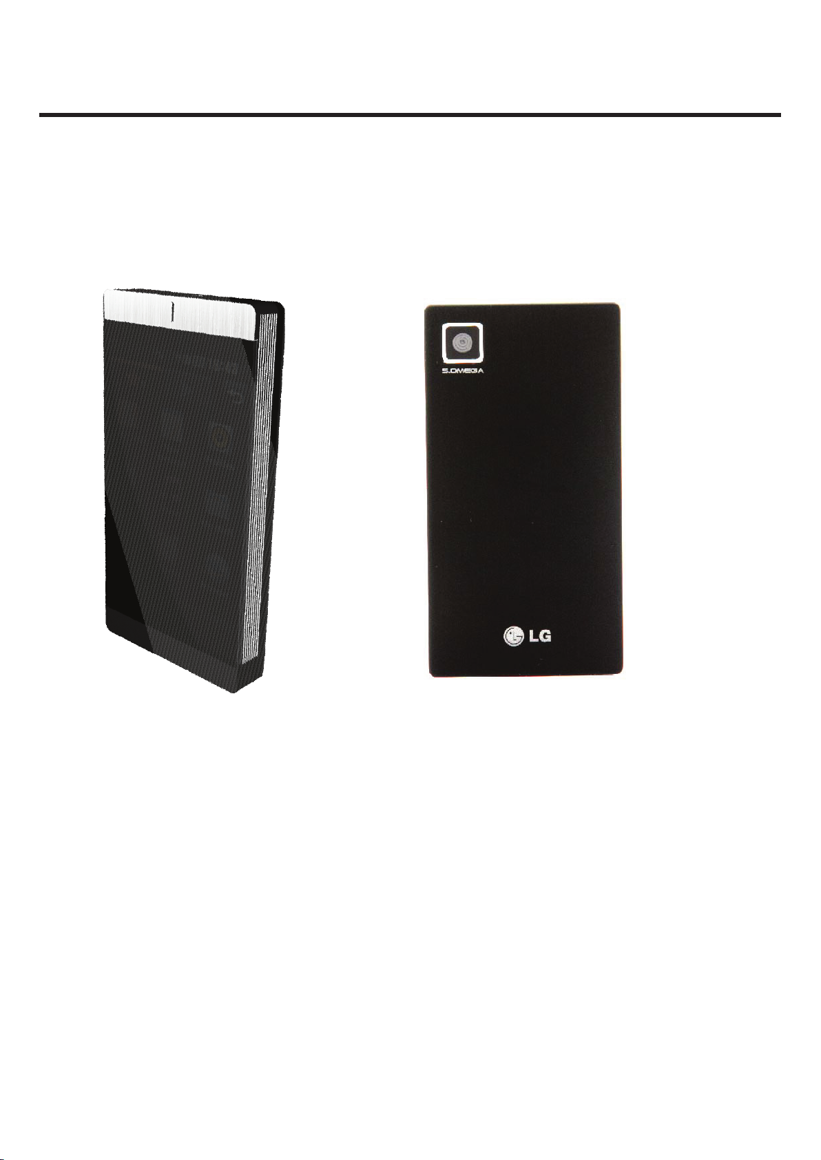
2.7 GD880 Figures
LGE Internal Use Only Copyright © 2010 LG Electronics. Inc. All right reserved.
- 20 -
Only for training and service purposes

ZUG{Gi
3. Technical Description
3.1 Digital Baseband(DBB/MSM7227)
3.1.1 General Description
A. Features(MSM7227)
WCDMA Rel ‘99 plus HSDPA and HSUPA
GSM/GPRS/EDGE
High-performance ARM1136JF-S™ application processor at up to 600 MHz; QDSP5000™ at 320 MHz
High-performance ARM926EJ-S™ modem processor at up to 400 MHz; QDSP4000™ at 122.88 MHz
Java® hardware acceleration for faster Java-based games and other applets
Support for Bluetooth® 2.1 EDR via an external Bluetooth System-on-Chip (SoC)
High-speed, serial mobile display digital interface (MDDI) that optimizes the interconnection
cost between the MSM device and the LCD panel
Receive diversity support for WCDMA mode, thereby providing improved capacity and data throughput
USB 2.0 compliant high-speed USB core with limited OTG capabilities
Integrated high-speed USB PHY
Integrated wideband stereo codec for digital audio applications
Direct interface to digital camera module with video front-end (VFE) image processing
GPS position location capabilities
Vocoder support (GSM-HR, FR, EFR, AMR, and AMR-WB/+)
Advanced 12 Ý 12 Ý1.05 mm, 0.4 mm pitch, 560 NSP
High-performance ARM1136JF-S 600 MHz application processor
Industry standard ARM926EJ-S 400 MHz embedded microprocessor subsystem
QDSP5000 320 MHz application digital signal processing (ADSP)
QDSP4000 122.88 MHz modem digital signal processing (MDSP)
256 kB internal memory (IMEM) for graphics, internal functions, DSP, etc.
Dual-memory buses separating the high-speed memory subsystem (EBI1) from low-speed
peripherals (EBI2) such as LCD panels
Enhanced EBI1 memory support: 200 MHz bus clock for DDR SDRAM
EBI2 support
All modes and data rates for WCDMA frequency division duplex (FDD), with the following restrictions
Full SF range support from 4 to 256
SMS (CS and PS)
PS data rate – 384 kb/s DL/384 kb/s UL
CS data rate – 64 kb/s DL/64 kb/s UL
AMR (all rates)
3. TECHNICAL BRIEF
3. TECHNICAL BRIEF
Copyright © 2010 LG Electronics. Inc. All right reserved.
Only for training and service purposes
- 21 -
LGE Internal Use Only
3. TECHNICAL BRIEF
3.2 Hardware Architecture
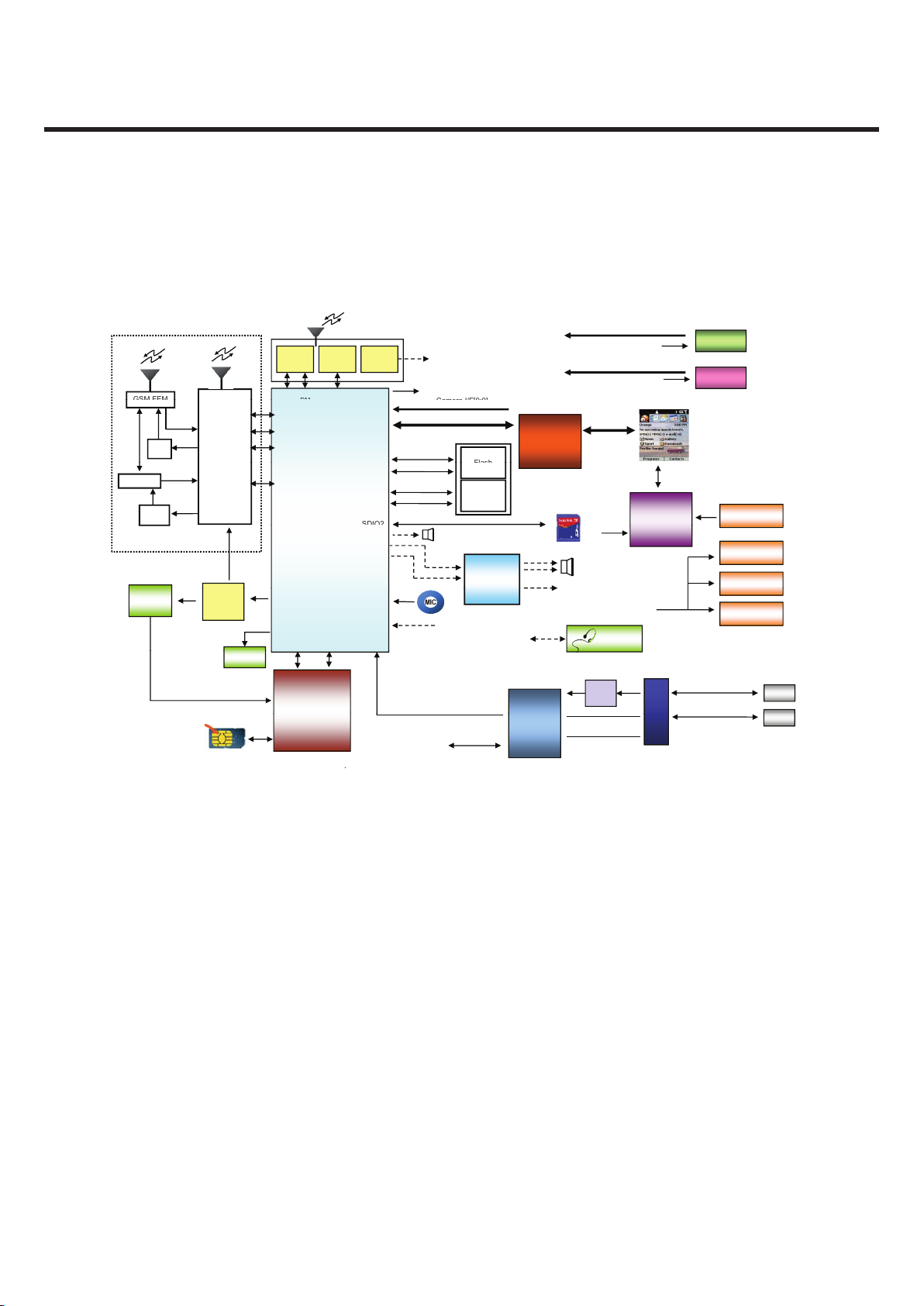
3. Technical Brief
MINI Block Diagram
Parallel Interface [0:9]
LBEH19UNBC
PCM
I2C
UART1/
WCDMA
GSM
VGA
Camera
5Mega AF
Camera
I2C
I2C
GPS
GPS
BT Wi-Fi
SDIO1
FM
FM Audio R/L
Parallel Interface [2:9]
MSM7227
CAM I/F
MCP
RX
SBI
GSM
850
900
1800
RX ADC
SSBI
EBI2 DATA
GSM FEM
RTR6285
DM
Camera I/F[0:9]
NAND
3.2” FWVGA LCD
MDDI
GPS
GPS ADC
RGB
Interface
RGB 24bit
EDGE
PAM
I2C
EBI2 ADDR
TX
WCDMA
900
2100
1900
TX DAC
EBI1 DATA
EBI1 ADDR
Duplexer
WCDM
A PAM
DDRSDRAM
2Gbit
Flash
4Gbit
Charge Pump
BD6084
LCD_PWM
Ambient Light
Sensor
RF Block
8CH
(ALC)
SDIO2
Speaker
Line O P/N
HPH_R/L
EAR1OP/N
Receiver
Micro SD
UART3/
UIM2
UART2/
DM
I2C
Touch
Sensor
Proximity
Speaker AMP
TCXO_RTR_19.2MHz
3.5ĭ
Earphone
PM_SSBI
USB I/F
MIC1P
UART2/UIM
I2C
Sensor
3-Axis
Sensor
PWM
Headset AMP
MIC2P
E
arphone
R/L
Audio Subsystem
Line L/R_IP
FM Audio R/L
Earphone R/L
TRK_LO_ADJ
GPS
D F/F
X-Tal
(19.2MHz)
PM7540
SSBI
cro USB
ector
USB 2.0 HS
USB
VBUS
OVP
Li
near
Motor
VCHG_VBUS
TCXO_PM_19.2MHz
USIM
USIM Translator
UART1/DM : BT
URRT2/DM : UART2(DP)
UART2/UIM : USIM
UART3/UIM2 : N.A
5pin Mi
Con
n
MUIC
UART
D+ / D-
UART3/UIM2
3.2 Hardware Architecture
3. Technical Brief
Figure. Simplified Block Diagram of System
LGE Internal Use Only Copyright © 2010 LG Electronics. Inc. All right reserved.
- 22 -
Only for training and service purposes
3. Technical Brief
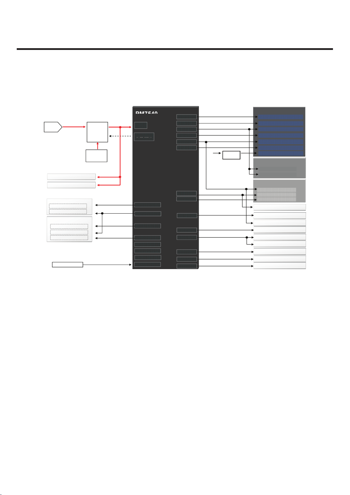
Figure. Simplified Block Diagram of System
<POWER Block1>
POWER Block
MSM7227
Charging IC
(NUS5530MN)
VCHG_VBUS
TA (5PIN)
5.1V,700mA
+VPWR
V
REG_MSMC1_1.35V (500m A)
VREG_MSME_1.8V (500m A)
VREG_MSMA_2.6V (300m A)
VDD
PM7540
VSW_MSME
VREG_MSMA
VSW_MSMC1
VSW_MSMC2
VREG_MSMC2_1.25V (500m A)
VDD_VCORE1 ( 1.2V , 203mA )
VDD_VCORE1 ( 1.2V , 203mA )
VDD_P1/P2/P8 /MDDI ( 1.8V ,MAX 10mA )
VDD_A / PLL ( 2,6V , MAX 65mA )
CHG_CTL_N
Battery
900mAh
VBATT
VREG_MSMP_2.6V (300m A)
VREG_MSMP
VREG_GP5
VREG_AUX2_2.9V (150m A)
VDD_P3/P4 (2.6V , MAX 25mA )
VDD_QFUSE (2.9V , MAX 10mA )
VDD_USBPHYE (3.3V , MAX 10mA )
USB
LDO(3.3V)
BATT_FET_N
+VPWR
MCP
SDRAM ( 1.8V , MAX 180mA )
NAND ( 1.8V , MAX 30mA )
RTR6285
GSM PAM
VDDA ( 2.7V , MAX 93mA )
VDDM ( 2.6V , MAX 10mA )
VDDA ( 2.1V , MAX 70mA )
VREG_RF_2.7V (150mA)
VREG_SMPS_2.1V (300mA)
VREG_RFRX1
VSW_PA
VREG_GP2
GPS LN
A
VREG_LCD_2.8V (150mA)
LCD module
VIO (1.8V )
WCDMA PAM
VREG_SYNT
VREG_MSME2
VREG_GP1
Motion Sensor ( 2.7V, MAX ?mA)
VREG_GP6
VREG_SENSOR_2.6V (300mA)
Proximity sensor( 2.7V, 20mA)
VREG_SYNTH_2.75V
VREG_LCD_1.8V (150mA)
VREG_RGBC_1.5V (150mA)
FEM
WVGA LCD Controller
CORE,DRAM,PLL,MD15 (1.5V )
VDD (2.8V )
VREG_RFTX
VREG_GP3
VREG_MMC_3.0V (150mA)
VREG_MMC MICRO SD slot (3.0V , , MAX mA )
VREG_TCXO_2.85V (50mA)
VREG_TCXO TCXO (2.85V , , MAX 20mA )
GPS D FLIP-FLOP
VREG_RGBC_2.6V (150mA)
MD18,PIO,HIO (1.8V
)
DRAM,OSC (2.6V )
VREG_RFRX2
USIM SLOT (3.0V , , 1mA )
V
REG_RUIM_3.0V (150mA)
VREG_RUIM1
VREG_MOTOR_3.0V (300mA)
Linear Motor Driver ( 3.0V, mA )
VREG_WLAN
VREG_GP4
BACKUP Battery
VBACK_UP
VCOIN
3. TECHNICAL BRIEF
Copyright © 2010 LG Electronics. Inc. All right reserved.
Only for training and service purposes
- 23 -
LGE Internal Use Only
3. TECHNICAL BRIEF
3. Technical Brief
Figure. Simplified Block Diagram of System
<Power Block2>
POWER Block
VREG_MSMP_2.6V
BD6084GUL
CAM_VDD_2.8V
CAM_VDD_1.8V
LDO2 (150mA)
LDO1 (150mA)
LDO3 (150mA)
5M CAMERA
VIO
CAM_AF_2.8V
+V_PWR
LDO4 (150mA)
VBAT
VGA CAMERA
Touch IC
TOUCH_VDD_3.3V
MLED ( 7ea )
MLEDOUT ( 450mA )
LCD_BACKLIGHT_4.8V
WIFI/BT/FM MODULE
VBAT
VDDIO/VDDIO_SD
VREG_MSMP_2.6V
LDO(2.8V)
26MHz TCXO for WIFI/BT/FM
MUIC
Audio Sub System
LGE Internal Use Only Copyright © 2010 LG Electronics. Inc. All right reserved.
- 24 -
Only for training and service purposes

3.3 Subsystem(MSM7227)
3.3.1 Architecture and baseband processing features
High-performance ARM1136JF-S 600 MHz application processor:
- ARM® architecture v6
- 32 kB instruction and 32 kB data cache
- 256 kB ARM11™ L2 cache
- 4 kB level-one tightly-coupled memory (TCM)
- 8-stage pipeline, branch prediction with return stack
- Supports the ARM and Thumb instruction sets, and Jazelle™ technology to enable direct
- execution of Java byte-codes
- Low-interrupt latency
Industry standard ARM926EJ-S 400 MHz embedded microprocessor subsystem
- 16 kB instruction and 16 kB data cache
- ARM version 5TEJ instructions
- Higher-performance five-stage pipeline, Harvard cached architecture
- Higher internal CPU clock rate with on-chip cache
- Internal watchdog and sleep timers
QDSP5000 320 MHz application digital signal processing (ADSP)
- 512 kB L2 cache
QDSP4000 122.88 MHz modem digital signal processing (MDSP)
3.3.2 Memory support features
256 kB internal memory (IMEM) for graphics, internal functions, DSP, etc.
Dual-memory buses separating the high-speed memory subsystem (EBI1) from low-speed peripherals
(EBI2) such as LCD panels
Enhanced EBI1 memory support: 200 MHz bus clock for DDR SDRAM
EBI2 support:
- 1.8 or 2.6 V memory interface support
- NAND/OneNAND™ flash memory interface
- Boot from NAND/OneNAND
- LCD and Universal Broadcast Modem™ (UBM™) support
3. Technical Brief
3. TECHNICAL BRIEF
Copyright © 2010 LG Electronics. Inc. All right reserved.
Only for training and service purposes
- 25 -
LGE Internal Use Only

3. TECHNICAL BRIEF
3.3.3 Air interface features
3.3.3.1 WCDMA R99
The MSM7227 device supports release 99, June 2004 of the WCDMA FDD standard, including
the following features.
All modes and data rates for WCDMA frequency division duplex (FDD), with the following restrictions:
- The downlink supports the following specifications.
: Up to four physical channels, including the broadcast channel (BCH), if present
: Up to three dedicated physical channels (DPCHs)
: Spreading factor (SF) range support from 4 to 256
: Support for the following transmit diversity modes:
=> Space-time transmit diversity (STTD)
=> Time-switched transmit diversity (TSTD)
=> Closed-loop feedback transmit diversity (CLTD)
- The uplink supports the following specifications.
: The uplink provides the following UE support.
=> One physical channel, eight TrCH, and 16 TrBks starting at any frame boundary
=> A maximum data rate of 384 kb/s
Full SF range support from 4 to 256
SMS (CS and PS)
PS data rate – 384 kb/s DL/384 kb/s UL
CS data rate – 64 kb/s DL/64 kb/s UL
AMR (all rates)
LGE Internal Use Only Copyright © 2010 LG Electronics. Inc. All right reserved.
- 26 -
Only for training and service purposes

3. TECHNICAL BRIEF
3.3.3.2 HSDPA
The MSM7227 device supports the release 5, December 2004 standard for HSDPA, including the
following features.
The HSDPA enables PS data speeds up to 7.2 Mb/s on the downlink.
HS-DSCH (HS-SCCH, HS-PDSCH, and HS-DPCCH) and the R99 transport channels, as defined in the 3GPP
specifications
A maximum of four simultaneous HS-SCCH channels, as defined in the 3GPP specifications
A maximum of 10 HS-PDSCH channels, both QPSK and 16 QAM modulation and UE category 6 in s
oftware release 2.0, and category 8 in software release 3.0
CQI and ACK/NACK on the HS-DPCCH channel, as defined in the 3GPP specifications
All incremental redundancy versions for HARQ, as defined in the 3GPP specifications
Can switch between HS-PDSCH and DPCH channel resources as directed by the network
Can be configured to support any of the two power classes 3 or 4, as defined in the 3GPP R5
specifications (25.101)
Network activation of compressed mode by SF/2 or HLS on the DPCH for conducting inter-frequency
or inter-RAT measurements when the HS-DSCH is active
STTD on both associated DPCH and HS-DSCH simultaneously
CLTD mode 1 on the DPCH when the HS-PDSCH is active
STTD on HS-SCCH when either STTD or CLTD mode 1 is configured on the associated DPCH
TFC selection limitation on the UL factoring in transmissions on the HS-DPCCH, as required in TS 25.133
3.3.3.3 HSUPA
The MSM7227 device supports the release 6, March 2006 standard for HSUPA, including the
following features.
E-DCH data rates of up to 5.76 Mb/s for 2 ms TTI (UE category 6) uplink
N E-AGCH, E-RGCH and E-HICH channels for downlink, as defined in the 3GPP specifications. E-RGCH and E-HICH
supports serving and non-serving radio links, with up to four radio links in the E-DCH active set.
STTD on all HSUPA downlink channels
CLTD mode 1 on HS-PDSCH and DPCH along with HSUPA channels
All incremental redundancy versions for HARQ and maximum number of HARQ retransmissions, as defined in
3GPP specifications
E-DCH channel on the uplink, as defined in the 3GPP specifications, with support for up to four E-DPDCH channels
HSUPA channels simultaneously with R99 and HSDPA channels, as defined in the 3GPP specifications
Switch between HSUPA channels and DPCH channel resources as directed by the network
Handover using compressed mode with simultaneous E-DCH and HS-DSCH interactive/background and
streaming QoS classes
ZUG{Gi
Copyright © 2010 LG Electronics. Inc. All right reserved.
Only for training and service purposes
- 27 -
LGE Internal Use Only

3. TECHNICAL BRIEF
3.3.3.4 GSM R99
The following GSM modes and data rates are supported by the MSM7227 hardware. Support modes
conform to release ‘99 specification of subfeatures.
Voice features
- FR, EFR, AMR, HR, A5/1 and A5/2 ciphering
Circuit-switched data features
- 9.6 k, 14.4 k, Fax
- Transparent and non-transparent modes for CS data and fax
- No subrates are supported.
3.3.3.5 GPRS
Packet-switched data (GPRS)
DTM (simple class A) operation
Multislot class 12 data services
CS schemes — CS1, CS2, CS3, and CS4
GEA1, GEA2, and GEA3 ciphering
Maximum of four Rx timeslots per frame
3.3.3.6 EDGE
EDGE E2 power class for 8 PSK
DTM (simple class A), multislot class 12
Downlink coding schemes — CS 1-4, MCS 1-9
Uplink coding schemes — CS 1-4, MCS 1-9
BEP reporting
SRB loopback and test mode B
8-bit and 11-bit RACH
PBCCH support
One-phase/two-phase access procedures
Link adaptation and IR
NACC, extended UL TBF
3. Technical Brief
LGE Internal Use Only Copyright © 2010 LG Electronics. Inc. All right reserved.
- 28 -
Only for training and service purposes

3. TECHNICAL BRIEF
3.3.3.7 GPS position location
Next-generation gpsOne® solution with an enhanced GPS engine
Enhanced filtering software optimizes GPS accuracy and availability.
Full integration with Windows Mobile®, Java, and BREW®-based development environments
MS-assisted, MS-based, MS-assisted/hybrid, and standalone GPS modes
gpsOneXTRA Assistance™ for enhanced standalone GPS performance
Support for UMTS control plane, GSM control plane, and OMA SUPL 1.0 user plane assisted-GPS protocols
3.3.4 Supported multimedia features
3.3.4.1 General multimedia
Additional general-purpose MIPS
- QDSP5000 aDSP at 320 MHz
- Dedicated hardware accelerators and compression engines
Improved Java, BREW, and game performance
3.3.4.2 Camera interface
High-quality digital camera processing, supporting CCD or CMOS image sensors up to 8-megapixels
Up to 12-bit data width with timing synchronization via discrete or embedded signals
YUV (4:2:2) or Bayer data types
A multitude of image signal processing capabilities
- Black level correction, bad pixel correction, and color correction
- Radial-based LROC, zoom, FOV crop, and frame drop
- Statistical techniques such as pre-zoom statistic gathering, AE/AWB, and histogram
- Gain adjustments including 4-channel and white balance
- Chroma subsampling, high-quality downscaler, and Bayer noise filter
ZUG{Gi
Copyright © 2010 LG Electronics. Inc. All right reserved.
Only for training and service purposes
- 29 -
LGE Internal Use Only

3. TECHNICAL BRIEF
3.3.4.3 Video
Dedicated support for market-leading codecs such as MPEG-4, H.263, H.264, and Windows Media®
- Integrated stereo wideband codec for music/digital clips
- CMX® – 128 polyphonic MIDI wavetable synthesizer
- Audio codecs: MP3, AMR-WB/+, AAC, AAC+™, EAAC+, and Windows Media
3.3.4.4 Graphics support
3D graphics core - Up to WVGA (800 Ý 480) display support
256 kB internal memory
3D support: OpenGL ES 1.1, 2.0, JSR 297, D3DM
2D support: OpenVG, SVG, JSR226, GDI, Ddraw
Performance:
- 27 megapixel triangles/s (peak 3D triangle rate)
- 166 megapixel/s peak 3D pixel draw rate
- 1660 megapixel/s effective 3D pixel rate
- 532 megapixel/s peak 3D pixel reject rate
- 207 megapixel four-component-vector instructions/s
- 166 megapixel/s 2D/OVG pixel draw rate
3.3.4.5 Audio processing
Integrated wideband stereo codec
- 16-bit DAC with typical 88 dB dynamic range
- Sampling rates up to 48 kHz on the speaker path and 48 kHz on the microphone path
- Supports summing of an external device’s stereo single-ended analog signal
- Supports summing of an I2S digital audio signal
- Supports headset switch press detection
Enhanced acoustic echo cancellation for full-duplex calls
PureVoice Audio AGC™
Internal vocoder supporting 13 kb/s PureVoice®
3.3.4.6 LCD controller
Parallel LCD support
RGB888 interface
3. Technical Brief
LGE Internal Use Only Copyright © 2010 LG Electronics. Inc. All right reserved.
- 30 -
Only for training and service purposes

3. TECHNICAL BRIEF
3.3.5 Supported connectivity features
High-speed USB port with integrated PHY
Four universal asynchronous receiver transmitter (UART) serial ports
- Two high-speed (DM via UART, 4 Mb/s)
- Emergency software download on UART2
Two UIM ports (shared with UART2 and UART3)
- 1.8 V and 3.0 V support; IS-820-C compliant
Four SDIO ports (SD 2.0)
- SD card, mini SD card, micro SD card, and MMC up to 52 MHz
- Boot from SD
Display support
- High-speed serial MDDI port that optimizes the interconnection cost between the MSM
device and LCD panel
- MDDI V1.0 interface that supports up to 384 Mb/s link rate
- Dual displays
: Primary => LCD controller (LCDC) or MDDI; FWVGA resolution; 16-bit, 18-bit, and 24-bit
true color depth; on-screen buffer support
: Secondary => EBI2 interface; up to WQVGA resolution; 16-bit, 18-bit, and 24-bit true
color depth
- Mobile display processor: MDP v.3
Touchscreen support
AUX_PCM for Bluetooth, SDAC, and SADC support
Inter-integrated circuit (I2C) interface for peripheral devices
Bluetooth 2.1 + EDR (external BTS4025™ IC)
Transport stream interface (TSIF) and the ability to support broadcast technologies, including the Qualcomm
MediaFLO™ technology, DVB-H, ISDB-T, T-DMB, and S-DMB
ZUG{Gi
Copyright © 2010 LG Electronics. Inc. All right reserved.
Only for training and service purposes
- 31 -
LGE Internal Use Only
 Loading...