

LG GD570 Service Manual

Service Manual Model : GD570
Internal Use Only
Service Manual
GD570
Date: June, 2010 / Issue 1.0

Table Of Contents
1. INTRODUCTION ..................................................................5
1.1 Purpose ............................................................................................... 5
1.2 Regulatory Information ............................................................... 5
1.3 Abbreviations ................................................................................... 7
2. PERFORMANCE ...................................................................9
2.1 Product Name .................................................................................. 9
2.2 Supporting Standard .................................................................... 9
2.3 Main Parts : GSM Solution ........................................................... 9
2.4 HW Features ....................................................................................10
2.5 SW Features ....................................................................................12
2.6 HW SPEC. .........................................................................................14
2.7 GD570 Figures ...............................................................................19
3. TECHNICAL BRIEF .............................................................20
3.1 GENERAL DESCRIPTION .............................................................20
3.2 GSM MODE ......................................................................................22
3.3 UMTS MODE ...................................................................................25
3.4 GPS MODE .......................................................................................28
3.5 LO GENERATION and DISTRIBUTION CIRCUIT ...................28
3.6 OFF-CHIP RF COMPONENTS ....................................................29
3.7 Digital Baseband(DBB/MSM6290) .........................................36
3.8 Hardware Architecture ...............................................................37
3.9 Subsystem(MSM6290) ................................................................39
3.10 Power Block ..................................................................................42
3.11 External memory interface ....................................................47
3.12 H/W Sub System .........................................................................50
3.13 Audio and sound ........................................................................58
3.14 Camera Interface ........................................................................65
3.15 Motion Sensor .............................................................................71
3.16 LG GD570 Main Features.........................................................72
3.17 Main Component .......................................................................73
4.5 Checking WCDMA Block ............................................................87
4.6 Checking GSM Block ................................................................ 100
4.7 Checking Bluetooth Block ..................................................... 109
4.8 Checking GPS Block ..................................................................112
4.9 Power ON Troubleshooting ...................................................114
4.10 Charger Troubleshooting .................................................... 116
4.11 USB Troubleshooting ............................................................. 119
4.12Audio trouble ............................................................................ 122
4. 13 3M Camera trouble shooting ............................................138
4.14 LCD trouble shooting ............................................................ 140
4.15 SIM Detect Troubleshooting ..............................................143
4.16 Keypad Backlight Troubleshooting .................................145
4.17 Coin type DC coreless MOTOR ........................................... 147
4.18 Motion Sensor on/off trouble ............................................149
5. DOWNLOAD ................................................................... 151
6. BLOCK DIAGRAM ........................................................... 164
7. CIRCUIT DIAGRAM ........................................................ 167
8. BGA Pin Map .................................................................. 177
9. PCB LAYOUT ................................................................... 183
10. RF CALIBRATION ......................................................... 191
10.1 Configuration of Tachyon .................................................... 191
10.2 How to use Tachyon ............................................................... 193
11. EXPLODED VIEW & REPLACEMENT
PART LIST .................................................................... 195
13.1 EXPLODED VIEW ......................................................................195
13.2 Replacement Parts..................................................................197
13.3 Accessory ...................................................................................223
4. TROUBLE SHOOTING .......................................................78
4.1 RF Component...............................................................................78
4.2 SIGNAL PATH ..................................................................................80
4.3 Checking TCXO Block ..................................................................83
4.4 Checking Front End Module (FEM) Block ...........................85
Copyright © 2010 LG Electronics. Inc. All right reserved.
Only for training and service purposes
- 3 -
LGE Internal Use Only

LGE Internal Use Only Copyright © 2010 LG Electronics. Inc. All right reserved.
- 4 -
Only for training and service purposes

1. INTRODUCTION
1.1 Purpose
This manual provides the information necessary to repair, calibration, description and download the
features of this model.
1.2 Regulatory Information
A. Security
Toll fraud, the unauthorized use of telecommunications system by an unauthorized part (for example,
persons other than your company’s employees, agents, subcontractors, or person working on your
company’s behalf) can result in substantial additional charges for your telecommunications services.
System users are responsible for the security of own system. There are may be risks of toll fraud associated
with your telecommunications system. System users are responsible for programming and configuring the
equipment to prevent unauthorized use. The manufacturer does not warrant that this product is immune
from the above case but will prevent unauthorized use of common-carrier telecommunication service of
facilities accessed through or connected to it.
The manufacturer will not be responsible for any charges that result from such unauthorized use.
B. Incidence of Harm
If a telephone company determines that the equipment provided to customer is faulty and possibly
causing harm or interruption in service to the telephone network, it should disconnect telephone service
until repair can be done. A telephone company may temporarily disconnect service as long as repair is not
done.
C. Changes in Service
A local telephone company may make changes in its communications facilities or procedure. If these
changes could reasonably be expected to affect the use of the this phone or compatibility with the
network, the telephone company is required to give advanced written notice to the user, allowing the user
to take appropriate steps to maintain telephone service.
D. Maintenance Limitations
Maintenance limitations on this model must be performed only by the manufacturer or its authorized
agent. The user may not make any changes and/or repairs expect as specifically noted in this manual.
Therefore, note that unauthorized alternations or repair may affect the regulatory status of the system and
may void any remaining warranty.
1. INTRODUCTION
1. INTRODUCTION
Copyright © 2010 LG Electronics. Inc. All right reserved.
Only for training and service purposes
- 5 -
LGE Internal Use Only

1. INTRODUCTION
E. Notice of Radiated Emissions
This model complies with rules regarding radiation and radio frequency emission as defined by local
regulatory agencies. In accordance with these agencies, you may be required to provide information such
as the following to the end user.
F. Pictures
The pictures in this manual are for illustrative purposes only; your actual hardware may look slightly
different.
G. Interference and Attenuation
Phone may interfere with sensitive laboratory equipment, medical equipment, etc.Interference from
unsuppressed engines or electric motors may cause problems.
H. Electrostatic Sensitive Devices
ATTENTION
Boards, which contain Electrostatic Sensitive Device (ESD), are indicated
by the sign. Following information is ESD handling:
• Service personnel should ground themselves by using a wrist strap when exchange system boards.
• When repairs are made to a system board, they should spread the floor with anti-static mat
which is also grounded.
• Use a suitable, grounded soldering iron.
• Keep sensitive parts in these protective packages until these are used.
• When returning system boards or parts like EEPROM to the factory, use the protective
package as described.
2. INTRODUCTION
LGE Internal Use Only Copyright © 2010 LG Electronics. Inc. All right reserved.
- 6 -
Only for training and service purposes

1.3 Abbreviations
For the purposes of this manual, following abbreviations apply:
Offset Phase Locked LoopOPLL
Light Emitting DiodeLED
Low Drop OutputLDO
Liquid Crystal DisplayLCD
Intermediate FrequencyIF
International Portable User IdentityIPUI
Global System for Mobile CommunicationsGSM
General Purpose Interface BusGPIB
Gaussian Minimum Shift KeyingGMSK
Flexible Printed Circuit BoardFPCB
Electrostatic DischargeESD
Electrical Erasable Programmable Read-Only MemoryEEPROM
Digital Signal ProcessingDSP
dB relative to 1 milli wattdBm
Digital Communication SystemDCS
Digital to Analog ConverterDAC
Constant Current – Constant VoltageCC-CV
Bit Error RatioBER
BasebandBB
Automatic Power ControlAPC
1. INTRODUCTION
1. INTRODUCTION
Copyright © 2010 LG Electronics. Inc. All right reserved.
Only for training and service purposes
- 7 -
LGE Internal Use Only

1. INTRODUCTION
Wireless Application Protocol
WAP
Voltage Control Temperature Compensated Crystal OscillatorVCTCXO
Voltage Controlled OscillatorVCO
Universal Asynchronous Receiver/TransmitterUART
Time Division Multiple AccessTDMA
Time Division DuplexTDD
Travel AdapterTA
Side Tone Masking RatingSTMR
Pseudo SRAMPSRAM
Static Random Access MemorySRAM
Sending Loudness RatingSLR
Subscriber Identity ModuleSIM
Surface Acoustic WaveSAW
Real Time ClockRTC
Root Mean SquareRMS
Receiving Loudness RatingRLR
Radio FrequencyRF
Public Switched Telephone NetworkPSTN
Phase Locked LoopPLL
Programmable Gain AmplifierPGA
Printed Circuit BoardPCB
Power Amplifier ModulePAM
1. INTRODUCTION
LGE Internal Use Only Copyright © 2010 LG Electronics. Inc. All right reserved.
- 8 -
Only for training and service purposes
2. PERFORMANCE
2.1 Product Name
GD570 : WCDMA1700/2100+GSM850/EGSM/DCS/PCS
(HSDPA 7.2Mbps / GPRS Class 10 / EDGE Class 10)
2.2 Supporting Standard
Item Feature Comment
Supporting Standard WCDMA(FDD1,4)/EGSM/GSM850/DCS1800/PCS1900 with
seamless handover
Phase 2+(include AMR)
SIM Toolkit : Class 1, 2, 3, C
Frequency Range WCDMA(FDD1) TX : 1920 – 1980 MHz
WCDMA(FDD1) RX : 2100 – 2170 MHz
WCDMA(FDD4) TX : 1710 – 1755 MHz
WCDMA(FDD4) RX : 2110 – 2155 MHz
GSM850 TX : 824 – 849 MHz
GSM850 RX : 869 – 894 MHz
EGSM TX : 880 – 915 MHz
EGSM RX : 925 – 960 MHz
DCS1800 TX : 1710 – 1785 MHz
DCS1800 RX : 1805 – 1880 MHz
PCS1900 TX : 1850 – 1910 MHz
PCS1900 RX : 1930 – 1990 MHz
Application Standard WAP 2.0, JAVA MIDP V2.1
2.3 Main Parts : GSM Solution
Item Part Name Comment
Digital Baseband MSM6290 : Qualcomm
Analog Baseband PM6658 : Qualcomm
RF Chip RTR6285 : Qualcomm
2. PERFORMANCE
Copyright © 2010 LG Electronics. Inc. All right reserved.
Only for training and service purposes
- 9 -
LGE Internal Use Only
2. PERFORMANCE
2.4 HW Features
Item Feature Comment
Form Factor Folder type
1) Capacity
Standard : Li-Ion, 900mAh
Battery
2) Packing Type : Soft Pack
Size Standard :
108.4 x 51.5 x 14.4mm
Weight 3.49 oz With Battery
Volume 80.39cc
PCB All Layer (10) , 0.8T
Stand by time 2G Over 400 hrs
3G Up to 340 hrs
@ Paging Period 5 (2G)
@ DRX 7 (3G)
Charging time 2.5 hrs @ Power Off / 550mA
Talk time 2G Up to 320mins
3G Up to 270 mins
@ Power Level 1 (2G/PCS)
@ Tx = 12dBm (3G)
RX sensitivity WCDMA(FDD1) : -106.7 dBm
WCDMA(FDD4) : -106.7 dBm
EGSM : -105 dBm
GSM850 : -105 dBm
DCS 1800 : -105 dBm
PCS 1900 : -105 dBm
WCDMA/
GSM/
GPRS
WCDMA : 24dBm/3.84MHz,+1/-3dBm
EGSM : 33dBm
GSM850 : 33 dBm
DCS 1800 : 30 dBm
PCS 1900 : 30 dBm
Class3(WCDMA)
Class4 (EGSM)
Class4 (GSM850)
Class1 (PCS)
Class1 (DCS)
TX
output
power
EDGE EGSM : 27 dBm
GSM 850 : 27 dBm
DCS 1800 : 26 dBm
PCS 1900 : 26 dBm
E2 (EGSM)
E2 (GSM850)
E2 (PCS)
E2 (DCS)
GPRS compatibility GPRS Class 10
EDGE compatibility EDGE Class 10
SIM card type Plug-In SIM
3V /1.8V
Display Main LCD
TFT Main LCD(2.8’, 240 x 400)
Built-in Camera 2M CMOS Fixed Focus Camera
Status Indicator Yes
Keypad Function Key : 24
Side Key : 3
Function Key: Call, Back, End,
Soft left/right, Voicemail,
Alphanumeric, Multitasking key,
#, *
Side Key : CAM, Multi, Volume up
/down
LGE Internal Use Only Copyright © 2010 LG Electronics. Inc. All right reserved.
- 10 -
Only for training and service purposes

2. PERFORMANCE
Item Feature Comment
ANT Main : Internal Fixed Type
BT : Internal Chip Type
GPS : Internal Fpcb Type
System connector 5 Pin
Ear Phone Jack 5 Pin
PC synchronization No
Memory NAND Flash : 2Gbit
SDRAM : 1Gbit
Speech coding FR, EFR, HR,AMR
Data & Fax Built in Data & Fax Not support
Vibrator Built in Vibrator
BlueTooth V2.1+ EDR
MIDI(for Buzzer
Function)
SW Decoded 72Poly
Music Player MP3/AAC/AAC+
Video Player MPEG4, H.263, H.264
Camcorder MPEG4, H.263
Voice Recording Yes
Speaker Phone mode
Support
Yes
Travel Adapter Yes Cableless
CDROM No No in Box
Stereo Headset Yes
Data Cable Yes
T-Flash
(External Memory)
No No in Box
Copyright © 2010 LG Electronics. Inc. All right reserved.
Only for training and service purposes
- 11 -
LGE Internal Use Only
2. PERFORMANCE
2.5 SW Features
Item Feature Comment
RSSI 0 ~ 7 Levels
Battery Charging 0 ~ 3 Levels
Key Volume 0 ~ 7 Levels
Audio Volume 1 ~ 7 Levels
Time / Date Display Yes
Multi-Language Yes English/Spanish/French
Quick Access Mode Dialing / Contact / Web2go / Menu /
Faves/ Message / Camera /Call history
Hot Key & 5-Way Navi Key
Speed Dial Yes (1~9) Voice mail center -> 1 key
CLIP / CLIR Yes
Phone Book Picture + Name + 5 Numbers + 3 E-
mails + 3 Messengers + 4 Group Select
+ Web Address + Company + Address
+ Ringtone + Birthday + Anniversary
day + 1 Memo + External Display +
Secret Lighting
Total 1000 Member
Last Dial Number Yes Total Call DB Max 100
LDN (SIM) N/A
Last Received
Number
Yes Total Call DB Max 100
LDN (SIM) N/A
Last Missed Number Yes Total Call DB Max 100
LDN (SIM) N/A
Search by Name Name, Number and E-Mail
Group 30
Fixed Dial Number Yes
Service Dial Number Yes
Own Number Yes
Voice Memo Yes
Call Reminder Yes Minute Minder
Network Selection Automatic
Mute Yes
Call Divert Yes
Call Barring No
Call Charge (AoC) No
Call Duration Yes
SMS / EMS 500 EMS : Release4
(Except Text align)
SMS Over GPRS Yes
EMS Melody / Picture
Send / Receive / Save
No
Receive only
MMS MPEG4
Send / Receive / Save
Yes
Yes
Long Message MAX 1736 Characters SMS 12 pages (Sending)
Cell Broadcast No
Download Over the WAP
LGE Internal Use Only Copyright © 2010 LG Electronics. Inc. All right reserved.
- 12 -
Only for training and service purposes

2. PERFORMANCE
Item Feature Comment
Game Yes
Calendar Yes
Memo Yes Max 30
Task Yes Max 100
World Clock Yes
Unit Convert Currency/Area/Length/Weight/Tempe
rature/ Volume/Velocity
Tip Calculator Yes
Stop Watch Yes
Wall Paper Yes
WAP Browser Over WAP 2.0 Obigo
Download Melody /
Wallpaper
Yes Over WAP
SIM Lock Yes Operator Dependent
SIM Toolkit Class 1, 2, 3, C
MMS Yes
EONS Yes
CPHS Yes Compliant with TMUS Spec.
ENS No
Camera Yes 3M / Digital Zoom : x2 / Multi-Shot
JAVA Yes CLDC V1.1 / MIDP V2.1
Download Over WAP
Voice Dial No
IrDa No
Bluetooth Yes V2.1 + EDR, HSP, HFP, OPP, OBEX,
BPP, PBAP, A2DP, AVRCP, FTP
(Server)
FM radio No
GPRS Yes Class 10
EDGE Yes Class 10
Hold / Retrieve Yes
Conference Call Yes Max 6 (Including owner)
DTMF Yes
Memo Pad Yes
TTY Yes No in box (mode support)
AMR Yes
SyncML Yes
IM Yes
Email Yes Native Client
Copyright © 2010 LG Electronics. Inc. All right reserved.
Only for training and service purposes
- 13 -
LGE Internal Use Only

2. PERFORMANCE
2.6 HW SPEC.
1) GSM transceiver specification
Item Specification
Phase Error
Rms : 5°
Peak : 20 °
Frequency Error
GSM : 0.1 ppm
DCS/PCS : 0.1 ppm
EMC(Radiated Spurious Emission
Disturbance)
GSM/DCS : < -28dBm
T
ransmitter Output power and Burst
Timing
GSM : 5dBm – 33dBm ± 3dB
DCS/PCS : 0dBm – 30dBm ± 3dB
Burst Timing <3.69us
Spectrum due to modulation out to
less than 1800kHz offset
200kHz : -36dBm
600kHz : -51dBm/-56dBm
Spectrum due to modulation out to
larger than 1800kHz offset to the
edge of the transmit band
GSM850
1800-3000kHz :< -63dBc(-46dBm)
3000kHz-6000kHz : <-65dBc(-46dBm)
6000kHz < : < -71dBc(-46dBm)
PCS :
1800-3000kHz :< -65dBc(-51dBm)
6000kHz < : < -73dBc(-51dBm)
Spectrum due to switching transient
400kHz : -19dBm/-22dBm(5/0), -23dBm
600kHz : -21dBm/-24dBm(5/0), -26dBm
Reference Sensitivity – TCH/FS Class II(RBER) : -105dBm(2.439%)
Usable receiver input level range 0.012(-15 - -40dBm)
Intermodulation rejection – Speech
channels
± 800kHz, ± 1600kHz
: -98dBm/-96dBm (2.439%)
AM Suppression
T GSM : -31dBm
- DCS : -29dBm
-98dBm/-96dBm (2.439%)
Timing Advance ± 0.5T
LGE Internal Use Only Copyright © 2010 LG Electronics. Inc. All right reserved.
- 14 -
Only for training and service purposes
2) WCDMA transmitter specification
Item Specification
Transmit Frequency Band1 : 1920 – 1980 MHz
Band4 : 1710 – 1755 MHz
Maximum Output Power +24 dBm / 3.84 MHz, +1 / -3 dB
Frequency Error within ±0.1 PPM
Open Loop Power Control Normal Conditions : within ±9 dB,
Extreme Conditions : within ±12 dB
Minimum Transmit Power < -50 dBm /3.84 MHz
Occupied Bandwidth < 5 MHz at 3.84 Mcps (99% of power)
Adjacent Channel Leakage
Power Ratio (ACLR)
> 33 dB @ ±5 MHz,
> 43 dB @ ±10 MHz
Spurious Emissions
|f-fc| > 12.5 MHz
< -36 dBm / 1 kHz RW @ 9 kHz ≤ f < 150 kHz
< -36 dBm / 10 kHz RW @ 150 KHz ≤ f < 30 MHz
< -36 dBm / 100 kHz RW @ 30 MHz ≤ f < 1 GHz
< -30 dBm / 1 MHz RW @ 1 GHz ≤ f < 12.75 GHz
< -60 dBm / 3.84 MHz RW @ 869 MHz ≤ f ≤ 894 MHz
< -60 dBm / 3.84 MHz RW @ 1930 MHz ≤ f ≤ 1900 MHz
< -60 dBm / 3.84 MHz RW @ 2110 MHz ≤ f ≤ 2155 MHz
< -67 dBm / 100 kHz RW @ 925 MHz ≤ f ≤ 935 MHz
< -79 dBm / 100 kHz RW @ 935 MHz < f ≤ 960 GHz
< -71 dBm / 100 kHz RW @ 1805 MHz ≤ f ≤ 1880 MHz
< -41 dBm / 300 kHz RW @ 1884.5 MHz < f < 1919.6 MHz
Transmit Intermodulation < -31 dBc @ 5 MHz & < -41 dBc @ 10 MHz
when Interference CW Signal Level = -40 dBm
Error Vector Magnitude < 17.5 %, when Pout ≥ -20 dBm
Peak Code Domain Error
< -15 dB at Pout t -20 dBm
2. PERFORMANCE
Copyright © 2010 LG Electronics. Inc. All right reserved.
Only for training and service purposes
- 15 -
LGE Internal Use Only

2. PERFORMANCE
3) WCDMA receiver specification
Item Specification
Receive Frequency Band1 : 2100 – 2170 MHz
Band4 : 2100 – 2155 MHz
Reference Sensitivity Level Band1 : BER < 0.001 when Îor = -106.7 dBm / 3.84 MHz
Band4 : BER < 0.001 when Îor = -106.7 dBm / 3.84 MHz
Maximum Input Level BER < 0.001 when Îor = -25 dBm / 3.84 MHz
Adjacent Channel Selectivity
(ACS)
ACS > 33 dB where BER < 0.001 when
Îor = -92.7 dBm / 3.84 MHz
& Ioac = –52 dBm / 3.84 MHz @ ±5 MHz
Blocking Characteristic BER < 0.001 when Îor = -104.7 dBm / 3.84 MHz
& Iblocking = -56 dBm / 3.84 MHz @ Fuw(offset) = ±10 MHz
or Iblocking = -44 dBm / 3.84 MHz @ Fuw(offset) = ±15 MHz
Spurious Response BER < 0.001 when Îor = -104.7 dBm / 3.84 MHz
& Iblocking = -44 dBm
Intermodulation BER < 0.001 when Îor= -104.7 dBm / 3.84 MHz
& Iouw1 = -46 dBm @ Fuw1(offset) = ±10 MHz
& Iouw2 = -46 dBm / 3.84 MHz @ Fuw2(offset) = ±20 MHz
Spurious Emissions < -57 dBm / 100 kHz BW @ 9 kHz ≤ f < 1 GHz
< -47 dBm / 1 MHz BW @ 1 GHz ≤ f ≤ 12.75 GHz
Inner Loop Power Control
In Uplink
Adjust output(TPC command)
cmd 1dB 2dB 3dB
+1 +0.5/1.5 +1/3 +1.5/4
0 -0.5/+0.5 -0.5/+0.5 -0.5/+0.5
-1 -0.5/-1.5 -1/-3 -1.5/-4
group(10equal command group)
+1 +8/+12 +16/+24
LGE Internal Use Only Copyright © 2010 LG Electronics. Inc. All right reserved.
- 16 -
Only for training and service purposes
4) HSDPA transmitter specification
Item Specification
Transmit Frequency Band1 : 1920 – 1980 MHz
Band4 : 1710 – 1755 MHz
Maximum Output Power Sub-Test
1=1/15, 2=12/15 21~25dBm / 3.84 MHz
3=13/15 4=15/8 20~25dBm / 3.84 MHz
5=15/7 6=15/0 19~25dBm / 3.84 MHz
HS-DPCCH
Sub-test
in table
C.10.1.4
Power
step
Power step slot
boundary
Power
step size,
P [dB]
Transmitter power step
tolerance [dB]
1 Start of
Ack/Nack
6 +/- 2.3
2 Start of CQI 1 +/- 0.6
5
3 Middle of CQI 0 +/- 0.6
Spectrum Emission Mask
Sub-Test : 1=1/15, 2=12/15, 3=13/15, 4=15/8, 5=15/7, 6=15/0
Frequency offset
from carrier f
Minimum requirement Measurement Bandwidth
2.5 ~ 3.5 MHz
-35-15×(f-2.5)dBc
30 kHz
3.5 ~ 7.5 MHz
-35-1×(f-3.5)dBc
1 MHz
7.5 ~ 8.5 MHz
-35-10×(f-7.5)dBc
1 MHz
8.5 ~ 12.5 MHz -49dBc 1 MHz
Adjacent Channel Leakage
Power Ratio (ACLR)
Sub-Test : 1=1/15, 2=12/15, 3=13/15, 4=15/8, 5=15/7, 6=15/0
> 33 dB @ ±5 MHz
> 43 dB @ ±10 MHz
Error Vector Magnitude < 17.5 %, when Pout ≥ -20 dBm
2. PERFORMANCE
Copyright © 2010 LG Electronics. Inc. All right reserved.
Only for training and service purposes
- 17 -
LGE Internal Use Only
2. PERFORMANCE
5) HSDPA receiver specification
Item Specification
Receive Frequency
Band1 : 2100 – 2170 MHz
Band4 : 2100 – 2155 MHz
Maximum Input Level
(BLER or R), 16QAM Only
Sub-Test : 1=1/15, 2=12/15, 3=13/15, 4=15/8, 5=15/7, 6=15/0
BLER < 10% or R >= 700kbps
6) GPS receiver specification
Item
Specification
Receive Frequency 1574.42 MHz ~ 1576.42 MHz
Minimum Sensitivity 1 satellite ≥-142dBm, 7 satellites ≥ -147dBm at coarse time aiding
LGE Internal Use Only Copyright © 2010 LG Electronics. Inc. All right reserved.
- 18 -
Only for training and service purposes

2.7 GD570 Figures
2. PERFORMANCE
Copyright © 2010 LG Electronics. Inc. All right reserved.
Only for training and service purposes
- 19 -
LGE Internal Use Only

3. TECHNICAL BRIEF
G
TECHNICAL BRIEF
3.1 GENERAL DESCRIPTION
The GD570 supports UMTS-1700(Band IV), UMTS-2100(Band I), GSM-850, GSM-900, GSM-1800, and GSM1900 based GSM/GPRS/EDGE/UMTS. All receivers and the UMTS transmitter use the radioOne
1
Zero-IF
architecture to eliminate intermediate frequencies, directly converting signals between RF and baseband.
The quad-band GSM transmitters use a baseband-to-IF up-conversion followed by an offset phase-locked
loop that translates the GMSK-modulated or 8-PSK-modulated signal to RF.
[Figure 1-1] Block diagram of RF part
GGGGGGGGGGGGGGGGGGGGGGGGGGGGGGGGGGGGGGGG GGGG
1
QUALCOMM’s branded chipset that implements a Zero-IF radio architecture.
G
2. RTR6285 and RF
Main_Ant
HB_RF_OUT2
HB_RF_OUT3
W2100
PAM
W(AWS)
DUPLEXER
W2100
DUPLEXER
Coupler
Coupler
W(AWS)
PAM
WCDMA
TX SAW
WCDMA
TX SAW
LB_RF_OUT2
TX_BIAS
I_IP_CH0
I_IM_CH0
Q_IP_CH0
PDET_IN
PRX_IP
PRX_IN
PRX
Q
P
DRX_IP
DRX_IN
WPRXHBP
WPRXHBN
WPRXLBP
WPRXLBN
WPRXSE2_IN
DRX_QP
DRX_QN
Q_IM_CH0
I_IP_CH1
I_IM_CH1
Q_IP_CH1
Q_IM_CH1
_
Q
PRX_QN
FRONT
END
Rx SAW
LNA
RTR6285
TX_IP
TX_IN
LB_RF_OUT1
GPS_IN
TX_QP
I_OUT
I_OUT_N
Q_OUT
Rx SAW
LNA
WDRXHB2
GPS_Ant
MODULE
G850/EGSM
PAM
GCELL_INP
GCELL_INN
EGSM INP
HB_RF_OUT1
RF_ON
DAC_IREF
SBDT
TX_QN
SBST
TX_ON
DAC_REF
Q_OUT_N
GSM 850
RX SAW
DCS/PCS
PAM
_
EGSM_INN
DCS_INP
DCS_INN
GPCS_INP
GPCS INN
WPRXSE2_OUT
VDDA
UMTS
Rx SAW
WB_MX_INM
WB_MX_INP
GSM 900
RX SAW
DCS1800
RX SAW
PCS1900
MSM6290
_
RX SAW
3. TECHNICAL BRIEF
LGE Internal Use Only Copyright © 2010 LG Electronics. Inc. All right reserved.
- 20 -
Only for training and service purposes

3. TECHNICAL BRIEF
G
A generic, high-level functional block diagram of GD570 is shown in Figure 1-1. Two antenna collects base
station forward link signals and radiates handset reverse link signals. The antenna connects with receive and
transmit paths through a FEM(Front End Module). The UMTS receive paths each include an LNA, an RF bandpass filter, and a downconverter that translate the signal directly from RF-to-baseband using radioOne ZIF
techniques.
The RFIC’s RX analog baseband outputs, for the receive chains, connect to the MSM IC. The UMTS and GSM RX
baseband outputs share the same inputs to the MSM IC.
For the transmit chains, the RTR6285 IC directly translates the TX baseband signals (from the MSM device) to
an RF signal using an internal LO generated by integrated on-chip PLL and VCO. The RTR6285 IC outputs
deliver fairly high-level RF signals that are first filtered by TX SAWs and then amplified by their respective
UMTS PAs.
In the GSM receive path, the received RF signals are applied through their band-pass filters and downconverted directly to baseband in the RTR6285 transceiver IC. These baseband outputs are shared with the
UMTS receiver and routed to the MSM IC for further signal processing.
The GSM/EDGE transmit path employs one stage of up-conversion and, in order to improve efficiency, is
divided into phase and amplitude components to produce an open-loop Polar topology:
1. The on-chip quadrature up-converter translates the GMSK-modulated signal or 8-PSK modulated signal, to
a constant envelope phase signal at RF;
2. The amplitude-modulated (AM) component is applied to the ramping control pin of Polar power amplifier
from a DAC within the MSM
GD570 power supply voltages are managed and regulated by the PM6658 Power Management IC. This
versatile device integrates all wireless handset power management, general housekeeping, and user
interface support functions into a single mixed signal IC. It monitors and controls the external power source
and coordinates battery recharging while maintaining the handset supply voltages using low dropout,
programmable regulators.
The device’s general housekeeping functions include an ADC and analog multiplexer circuit for monitoring
on-chip voltage sources, charging status, and current flow, as well as user-defined off-chip variables such as
temperature, RF output power, and battery ID. Various oscillator, clock, and counter circuits support IC and
higher-level handset functions. Key parameters such as under-voltage lockout and crystal oscillator signal
presence are monitored to protect against detrimental conditions.
Copyright © 2010 LG Electronics. Inc. All right reserved.
Only for training and service purposes
- 21 -
LGE Internal Use Only
3. TECHNICAL BRIEF
G
3.2 GSM MODE
3.2.1 GSM RECEIVER
The GSM-850, GSM-900, GSM-1800, and GSM-1900 receiver inputs of RTR6285 are connected directly to the
transceiver front-end circuits (filters and antenna switch module). GSM-850, GSM-900, GSM-1800, and GSM1900 receiver inputs use differential configurations to improve common-mode rejection and second-order
non-linearity performance as shown in Figure 1-2. The balance between the complementary signals is critical
and must be maintained from the RF filter outputs all the way into the IC pins
[Figure 1-2] GSM Receiver Inputs Topologies
LGE Internal Use Only Copyright © 2010 LG Electronics. Inc. All right reserved.
- 22 -
Only for training and service purposes

3. TECHNICAL BRIEF
G
Since GSM-850, GSM-900, GSM-1800, and GSM-1900 signals are time-division duplex (the handset can only
receive or transmit at one time), switches are used to separate RX and TX signals in place of frequency
duplexers – this is accomplished in the switch module. The GSM-850, GSM-900, GSM-1800, and GSM-1900
receive signals are routed to the RTR6285 through band selection filters and matching networks that
transform single-ended 50-Ωҏsources to differential impedances optimized for gain and noise figure. The RTR
input uses a differential configuration to improve second-order inter-modulation and common mode
rejection performance. The RTR6285 input stages include MSM-controlled gain adjustments that maximize
receiver dynamic range.
The amplifier outputs drive the RF ports of the quadrature RF-to-baseband downconverters. The
downconverted baseband outputs are multiplexed and routed to lowpass filters (one I and one Q) having
passband and stopband characteristics suitable for GMSK or 8-PSK processing. These filter circuits include DC
offset corrections. The filter outputs are buffered and passed on to the MSM6290 IC for further processing as
shown in Figure 1-5.
Copyright © 2010 LG Electronics. Inc. All right reserved.
Only for training and service purposes
- 23 -
LGE Internal Use Only
3. TECHNICAL BRIEF
G
3.2.2 GSM TRANSMITTER
The RTR6285 transmitter outputs(HB_RF_OUT1 and LB_RF_OUT1) include on-chip output matching
inductors. 50ohm output impedance is achieved by adding a series capacitor at the output pins. The
capacitor value may be optimized for specific applications and PCB characteristics based on pass-band
symmetry about the band center frequency as shown in Figure 1-3.
G
[Figure 1-3] GSM Transmitter Outputs Topologies
The RTR6285 IC is able to support GSM 850/900 and GSM 1800/1900 mode transmitting. Both high-band and
low band outputs are followed by resistive pads to ensure that the load presented to the outputs remains
close to 50ohm.
LGE Internal Use Only Copyright © 2010 LG Electronics. Inc. All right reserved.
- 24 -
Only for training and service purposes
3. TECHNICAL BRIEF
G
3.3 UMTS MODE
3.3.1 UMTS RECEIVER
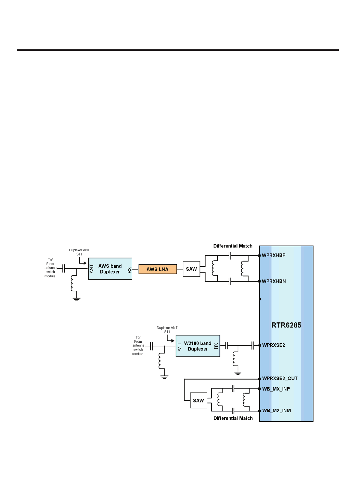
The AWS Band duplexer receiver output is routed to external LNA circuits and LNA circuits within the
RTR6285 device. Signal path received from diversity antenna is routed to external LNA circuits and LNA
circuits within the RTR6285 device as shown in Figure 1-4. External LNA circuits are used to improve RX
performance.
The UMTS primary RX input is provided with an on-chip LNA that amplifies the signal before a second stage
filter that provides differential down converter as shown in Figure 1-5. This second stage input is configured
differentially to optimize second-order inter-modulation and common mode rejection performance. The gain
of the UMTS front end amplifier and the UMTS second stage differential amplifier are adjustable, under MSM
control, to extend the dynamic range of the receivers.
The second stage UMTS RX amplifiers drive the RF ports of the quadrature RF-to-baseband down-converters.
The down-converted UMTS RX baseband outputs are routed to low-pass filters having pass-band and stopband characteristics suitable for UMTS RX processing. These filter circuits allow DC offset corrections, and
their differential outputs are buffered to interface shared with GSM RX to the MSM IC.
The UMTS baseband outputs are turned off when the RTR6285 is down-converting GSM signals and on when
the UMTS is operating.
[Figure 1-4] UMTS Receiver Inputs Topologies
Copyright © 2010 LG Electronics. Inc. All right reserved.
Only for training and service purposes
- 25 -
LGE Internal Use Only

3. TECHNICAL BRIEF
G
3.3.2 UMTS TRANSMITTER
The UMTS TX path begins with differential baseband signals (I and Q) from the MSM device.
These analog input signals are amplified, filtered, and applied to the quadrature up-converter mixers. The upconverter output is amplified by multiple variable gain stages that provide transmit AGC control. The AGC
output is filtered and applied to the driver amplifier; this output stage includes an integrated matching
inductor that simplifies the external matching network to a single series capacitor to achieve the desired 50Ω interface.
The RTR6285 UMTS output is routed to its power amplifier through a band pass filter, and delivers fairly highlevel signals that are filtered and applied to the PA. Transmit power is delivered from the duplexer to the
antenna through the switch module.
The transceiver LO synthesizer is contained within the RTR6285 IC with the exception of the off-chip loop
filter components and the VC-TCXO. This provides a simplified design for multimode applications. The PLL
circuits include a reference divider, phase detector, charge pump, feedback divider, and digital logic
generator.
UMTS TX. Using only PLL1, the LO generation and distribution circuits create the necessary LO signals for nine
different frequency converters. The UMTS transmitter also employs the ZIF architecture to translate the signal
directly from baseband to RF. This requires FLO to equal FRF, and the RTR6285 IC design achieves this without
allowing FVCO to equal FRF.
The RTR6285 IC is able to support UMTS 2100/1900/1800/1700 and 850 mode transmitting. This design
guideline shows only UMTS 1700 applications.
LGE Internal Use Only Copyright © 2010 LG Electronics. Inc. All right reserved.
- 26 -
Only for training and service purposes
3. TECHNICAL BRIEF
G
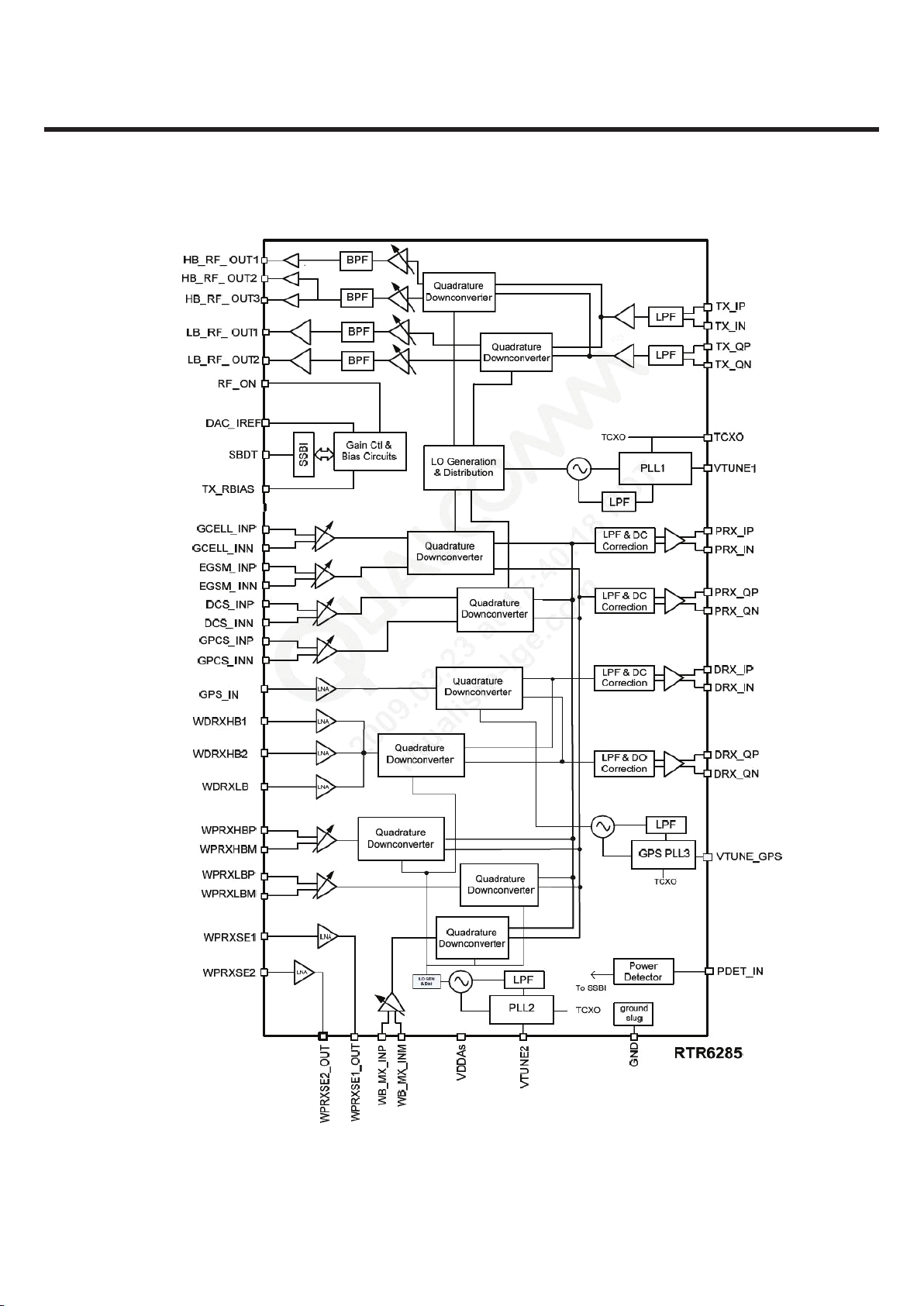
[Figure 1-5] RTR6285 IC Functional Block Diagram
Copyright © 2010 LG Electronics. Inc. All right reserved.
Only for training and service purposes
- 27 -
LGE Internal Use Only
3. TECHNICAL BRIEF
G
3.4 GPS MODE
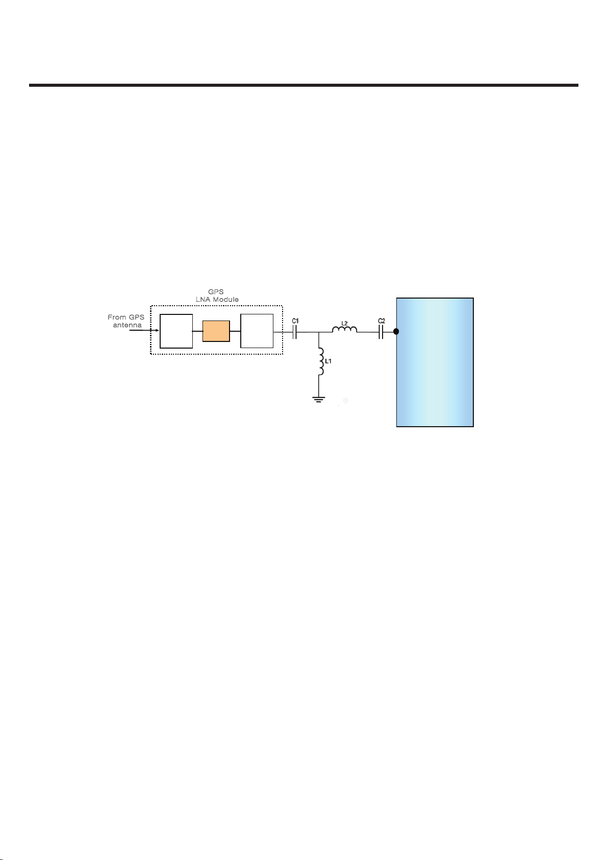
3.4.1 GPS RECEIVER
The GPS receiver input employs a single-ended connection realized by this pin. The GPS input is routed from
the GPS antenna, through external LNA included in a band-pass filter and then
an impedance transformer circuit that optimally matches the impedance looking into GPS LNA within the
RTR6285 device. The impedance transformer circuit topology is shown in Figure 1-6.
[Figure 1-6] GPS Input Network Topology
3.5 LO GENERATION and DISTRIBUTION CIRCUIT
The integrated LO generation and distribution circuits are driven by internal VCOs to support various modes
to yield highly flexible quadrature LO outputs that drive all GSM/EDGE, GPS and UMTS band up-converters
and down-converters; with the help of these LO generation and distribution circuits, true zero-IF architecture
is employed in all GSM and UMTS band receivers and transmitters to translate the signal directly from RF-tobaseband and from baseband-to-RF. Two fully functional fraction-N synthesizers, including VCOs and loop
filters, are integrated within the RTR6285 IC. In addition, the RTR6285 has a third synthesizer used for GPS
operation. The first synthesizer (PLL1) in the RTR6285 creates the transceiver Los that support the UMTS
transmitter, and all four GSM band receivers and transmitters including: GSM850, GSM900, GSM1800, and
GSM1900. The second synthesizer (PLL2) in the RTR6285 IC provides the LO for the UMTS primary receiver. For
the RTR6285 IC only, the second synthesizer also provides the LO for the secondary UMTS receiver. The third
synthesizer (PLL3), only in the RTR6285 IC, provides the LO for the GPS receiver. An external TCXO input signal
is required to provide the synthesizer frequency reference to which the PLL is phase and frequency locked.
The RTR6285 ICs integrate most of the PLL loop filter components on-chip except for three off-chip loop
filter-series capacitors, which significantly reduces off-chip component requirement. With the integrated
fractional-N PLL synthesizers, the RTR6285 ICs have the advantage of more flexible loop bandwidth control,
fast lock time, and low-integrated phase error.
G
RTR6285
GPS_IN
LNA
SAW
SAW
mGnwzG
nwzG
suhGt
LGE Internal Use Only Copyright © 2010 LG Electronics. Inc. All right reserved.
- 28 -
Only for training and service purposes
3. TECHNICAL BRIEF
G
3.6 OFF-CHIP RF COMPONENTS
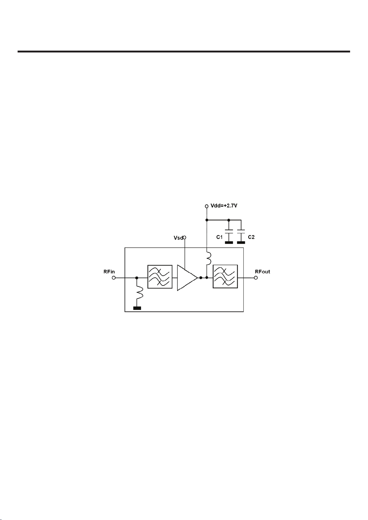
3.6.1 GPS LNA (U101: ALM-2712)
The ALM-2712 is an LNA module, with integrated filter, designed for GPS band applications at 1.575GHz. The
LNA uses AVAGO Technologies’ proprietary GaAs Enhancement-mode pHEMT process to achieve high gain
with very low noise figure and high linearity Noise figure distribution is very tightly controlled. A CMOScompatible shutdown pin is included either for turning the LNA on/off, or for current adjustment. The
integrated filter utilizes an Avago Technologies’ leading edge FBAR filter for exceptional rejection at Cell/PCS
Band frequencies. The ALM-2712 is useable down to 1V operation. It achieves low noise figure, high gain and
linearity even at 1V, making it suitable for use in critical low-power GPS applications or during low-battery
situations.
[Figure 1-7] ALM-2712 Functional Block Diagram.
3.6.2 AWS LNA (U1000 BGA711L7)
The BGA711L7 is a low current single-band low noise amplifier MMIC for UMTS bands I and IV. The LNA is
based upon Infineon’s proprietary and cost-effective SiGe:C technology and comes in a low profile TSLP-7-1
leadless green package. Because the matching is off chip, the 2100 MHz path can be easily converted into a
1900 MHz path by optimizing the input and output matching network.
In the main features of this module, Gain is 17dB and noise figure is 1.1dB in high gain mode. and, input
and output RF ports are matched to 50-Ωҏ
Copyright © 2010 LG Electronics. Inc. All right reserved.
Only for training and service purposes
- 29 -
LGE Internal Use Only

3. TECHNICAL BRIEF
G
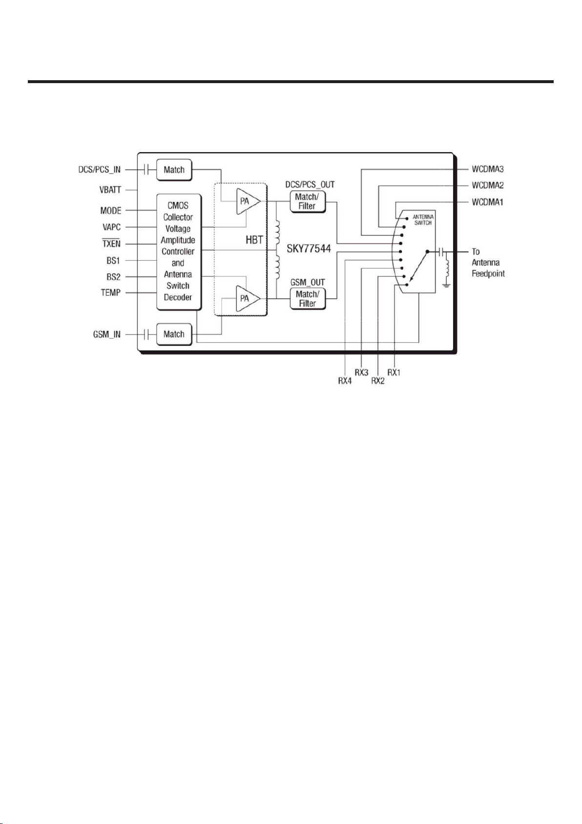
3.6.3 FEM, Front End Module (U1008: SKY77544)
The module consists of a GSM850/900 PA and DCS1800/PCS1900 PA block, impedance matching
circuitry for 50 ȳ input and output impedances, Tx harmonic filtering, high linearity low insertion loss
switches, and a CMOS Power Amplifier Control (PAC) block. A custom silicon integrated circuit contains
decoder circuitry to control the RF switch while providing a low current external control interface. An
integrated temperature sensor provides an analog voltage based on the temperature of the module.
Fabricated in InGaP/GaAs, the Hetero-junction Bipolar Transistor (HBT) PA blocks support the GSM850/900
bands and DCS1800/PCS1900 bands. Both PA blocks share common power supply pads to distribute current.
The output of the PA block and the outputs to the seven receive pads connect to the antenna pad through a
highly linear antenna switch. The WCDMA and Rx ports feature a 0 volts DC offset level, which eliminates any
need for external blocking capacitors. The InGaP/GaAs die, switch die, Silicon (Si) controller die, and passive
components are mounted on a multi-layer laminate substrate and the entire assembly is encapsulated with
plastic overmold.
RF input and output ports of the SKY77544 are internally matched to a 50 ȳ load to reduce the number of
external components for a quad-band design. Extremely low leakage current of the FEM maximizes handset
standby time. Band selection and control of transmit and receive RF signal flows are performed by use of four
external control pads. See Figure 1-6 shown on overleaf. Mode of operation Tx, Rx, Band (GSM850, GSM900,
DCS, PCS, and UMTS) is controlled with 4 logic inputs: BS1, BS2, Mode, and TxEN. Proper timing of the TxEN
input and the VAPC input ensures high isolation between the antenna and Tx-VCO while the VCO is being
tuned prior to the transmit burst. The Enable input controls the initial turn-on of the PAC circuitry to minimize
battery drain.
The integrated power amplifier control (PAC) function provides envelope amplitude control by
reducing sensitivity to input drive, temperature, power supply, and process variation.
ANT_SEL0 ANT_SEL1 ANT_SEL2 ANT_SEL3
GSM850_EGSM_TX LOW LOW LOW HIGH
DCS_PCS_TX LOW LOW HIGH HIGH
PCS_RX (RX1) HIGH LOW LOW LOW
DCS_RX (RX2) HIGH LOW LOW HIGH
EGSM_RX (RX3) HIGH LOW HIGH HIGH
GSM850_RX (RX4) HIGH LOW HIGH LOW
W1700 (WCDMA2) LOW HIGH LOW LOW
W2100 (WCDMA1) LOW LOW HIGH LOW
[Table 1] Antenna Switch Module Logic
LGE Internal Use Only Copyright © 2010 LG Electronics. Inc. All right reserved.
- 30 -
Only for training and service purposes
3. TECHNICAL BRIEF
G
[Figure 1- 8] SKY77544 Functional Block Diagram.
Copyright © 2010 LG Electronics. Inc. All right reserved.
Only for training and service purposes
- 31 -
LGE Internal Use Only
 Loading...