

LG GCE-8481B Service Manual

3
INTRODUCTION
FEATURES
1. General
1) Enhanced IDE interface.
2) Internal 5.25 inch, halfheight CD-R/RW Drive.
3) 2Mbytes buffer memory.
4) Audio CD like tray loading of a disc without using a caddy.
5) Power loading and power ejecting of a disc. The disc can also be ejected manually.
6) Supports Power saving mode and Sleep mode.
7) Vertical and Horizontal operation.
8) SuperLink Function.
2. Supported disc formats
1) Reads and writes data in each CD-ROM, CD-ROMXA, CD-I FMV, Video CD, and CD-EXTRA
2) Reads data in Photo CD (Single and Multi session).
3) Reads and writes standard CD-DA.
4) Reads and writes CD-R discs conforming to “Orange Book Part 2”.
5) Reads and writes CD-RW discs conforming to “Orange Book Parts 3”.
3. Supported write method
1) Disc at once (DAO), Session at once (SAO), Track at once (TAO), Variable packet, Fixed packet, and
Multi-session.
4. Performance
1) Random 100 ms average access time.
2) CD-R Record speed : 8X, 12X, 16X, 22X~40X (PCAV), 48X CAV.
3) CD-RW Record speed : 4X, 10X, 12X, 16X, X24(PCAV).
4) CD-ROM : Max 7,200 KB/s(Max 48x) Sustained Transfer rate.
5) Supports real time error correction and real time layered error correction at each speed.
6) PIO Mode 4, Multi DMA Mode 2, UDMA Mode 2.
7) Multimedia MPC-3 Spec compliant.
8) Support CD-TEXT read/write.
5. Audio
1) Output 16 bit digital data over ATA interface.
2) 8 Times Digital Filter for CD Audio
3) Software Volume Control
4) Equipped with audio line output and headphone jack for audio CD playback.
5) Front panel Volume Control for Headphone Output.
This service manual provides a variety of service
information.
It contains the mechanical structure of the CDR/RW Drive and the electronic circuits in
schematic form. This CD-R/RW Drive was
manufactured and assembled under our strict
quality control standards and meets or exceeds
industry specifications and standards.
This CD-R/RW drive is an internal drive unit
designed for use with IBM PC, HP Vectra, or
compatible computer. It can write as much as 700
Mbytes of digital data into CD-R/RW disc, and can
read as much as 650 Mbytes of digital data stored
in a CD-ROM, CD-R and CD-RW disc.
This CD-R/RW Drive can easily meet the
upcoming MPC level 3 specification, and its
Enhanced Intelligent Device Electronics (E-IDE)
and ATAPI interface allows Plug and play
integration in the majority of today’s PCs without
the need of an additional interface card.
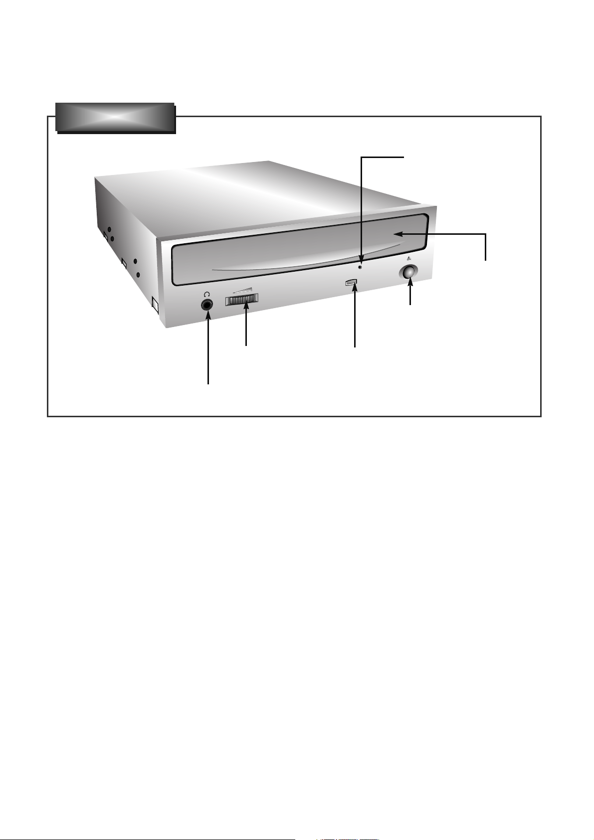
LOCATION OF CUSTOMER CONTROLS
6
1. Disc tray
This is the tray for the disc. Place the disc on the
ejected disc tray, then lightly push the tray (or
push the eject button) and the CD will be loaded.
NOTE: Don’t pull out or push in the disc tray
forcibly. This might cause damage to the loading
section of the drive.
2. Stop/Eject button
This button is pressed to open the CD tray.
This button works only when power is supplied to
the drive.
If an Audio CD is playing, pressing this button will
stop it, and pressing it again will open the tray.
3. Emergency Eject Hole
Insert a paper clip here to eject the Disc tray
manually or when there is no power.
4. Volume control
This is used to adjust the output volume of the
headphone jack. It can’t be used to adjust the
output volume for the audio output connectors on
the rear panel.
NOTE : Turn the volume down before turning on
the power. Sudden loud noises can damage your
hearing.
5. Headphone jack
This jack is for connecting headphones or minispeakers.
6. Drive activity indicator(Read/Write)
Two colored LED is used to indicate the operation
of CD-R/RW Drive.
Headphone Jack
Volume
Control
Drive Activity Indicator
Stop/Eject Button
Disc Tray
Emergency Eject Hole
Front Panel
7
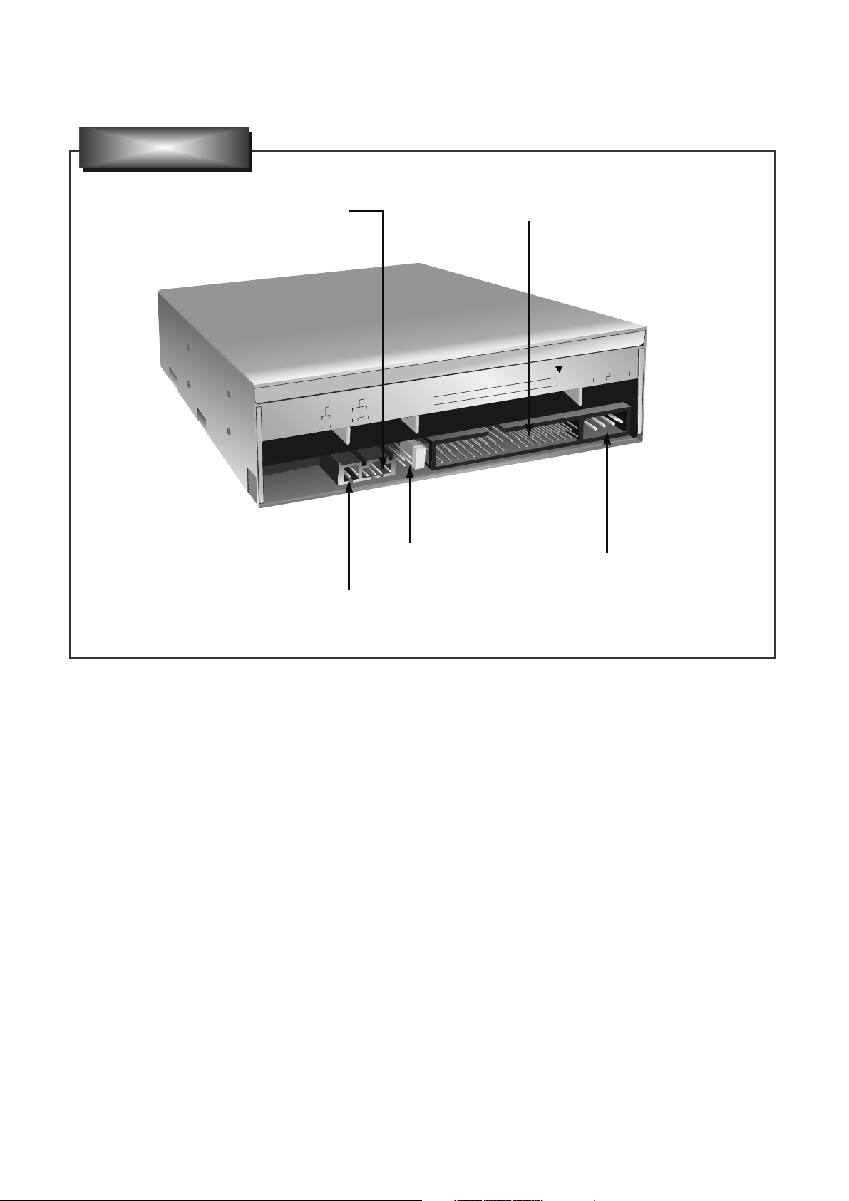
1. Power Connector
Connects to the power supply (5-and 12-V DC) of
the host computer.
NOTE : Be careful to connect with the proper
polarity. Connecting the wrong way may damage
the system (and is not guaranteed). Usually this
connector can only be attached one-way.
2. IDE Interface Connector
Connect to the IDE (Integrated Device
Electronics) Interface using a 40-pin flat IDE
cable.
NOTE : Do not connect or disconnect the cable
when the power is on, as this could cause a short
circuit and damage the system. Always turn the
power OFF when connecting or disconnecting the
cable.
3. Jumper Connector
This jumper determines whether the drive is
configured as a master or slave. Changing the
master-slave configuration takes effect after
power-on reset.
4. Analog Audio Output Connector
Provides output to a sound card (analog signal).
Generally you need this to play a regular audio
CD.
5. Digital Audio Output Connector
Provides output to a sound card (digital signal).
DIGITAL
AUDIO
ANALOG
AUDIO
INTERFACE
POWER
D G
39
40
1
+5
GND
+12
2
C S M
S L A
R G L
Digital Audio Output
Connector
Jumper Connector
Analog Audio Output Connector
IDE Interface Connector
Power Connector
Rear Panel
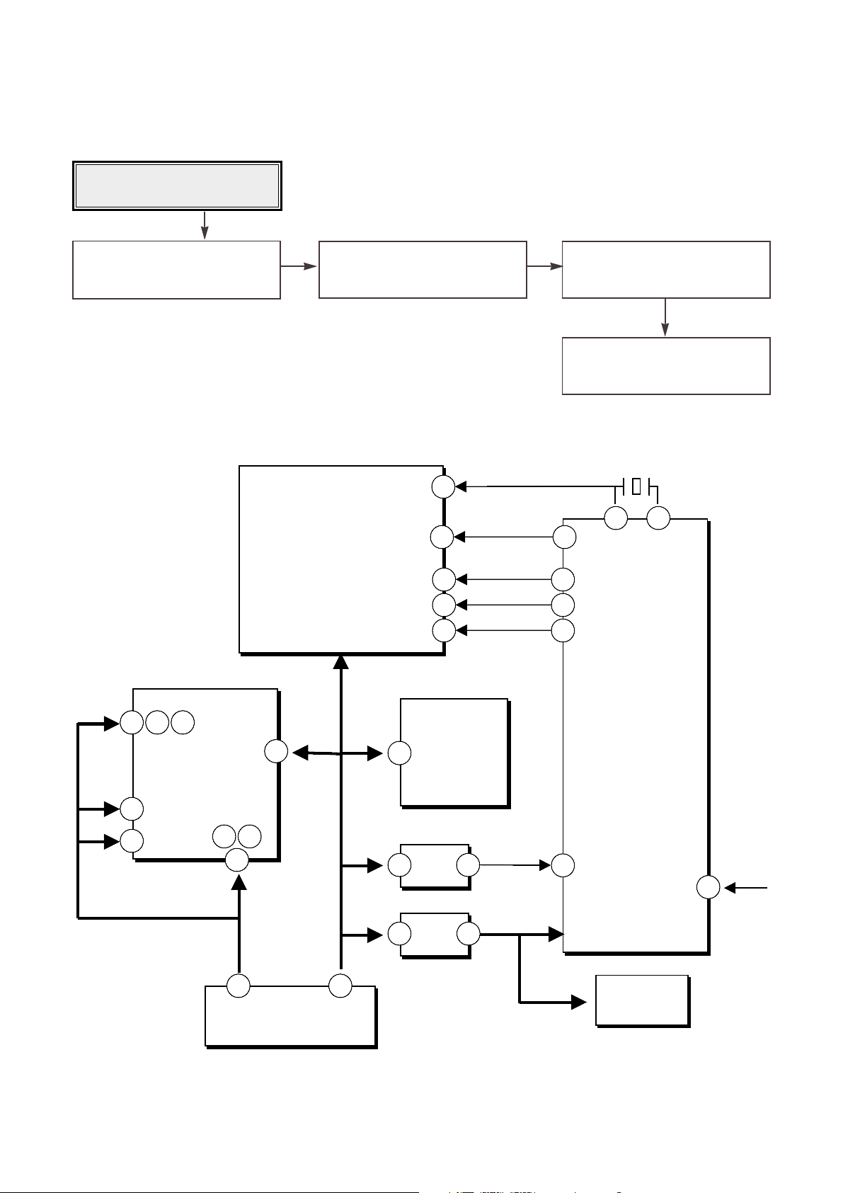
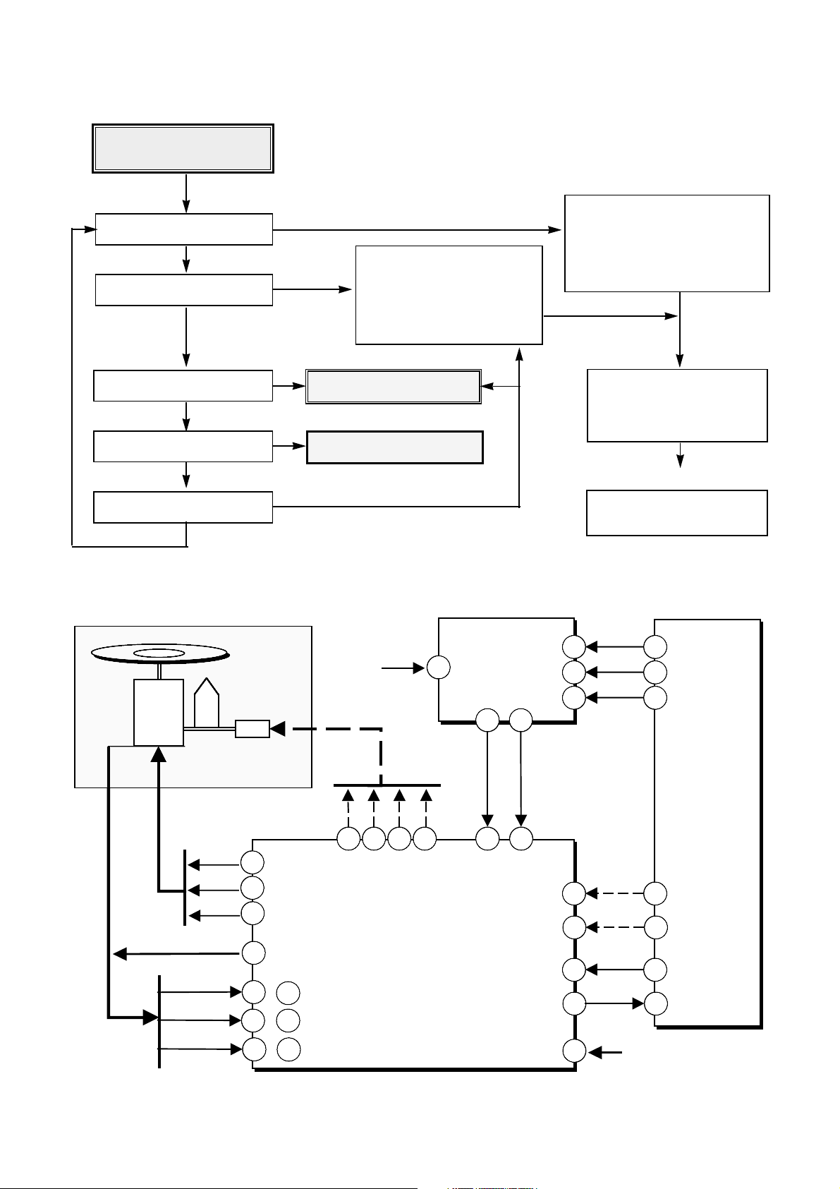
TROUBLESHOOTING GUIDE
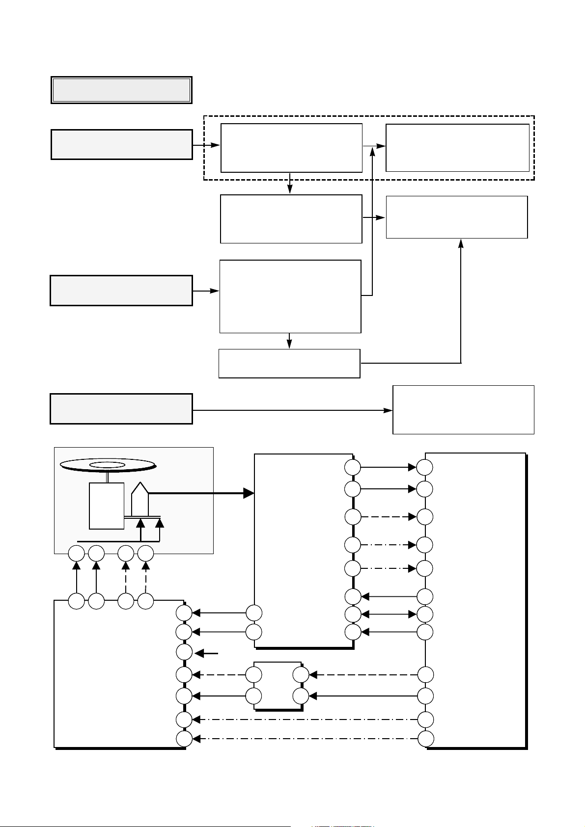
Power check
(Malfunction of LED and Tray).
52
Check the connection of 5V, 12V.
Check the Reset (Pin 170, 122 of
IC101, pin2 of IC401).
Check the input of oscillation (pin
109 of IC401).
Check SCLK, SDATA, XLAT
(pin 122, 123, 124 of IC401).
1. Connect only the power cable
BD7907FS
6Ch Servo DRIVE
MT1516
RF Amp
Wobble
ALPC
General port use
EEPROM access
MT1508
DSP
Decoder
Encoder
ATIP Demodulator
Write Strategy
Write S/H Signal
I / F
Micro Processor
33.868 8MHz
IC 101
IC 501
IC 103
IC 401
IC 102
3.3 V
Reset
12V 5V
AT49F002N
512KB
Flash ROM
IC 502
41
109
44
2
54
31
3
32
10 19 20
31
32
30
44 51
IC 202
2 170
PRST
‘ L ’
122
/ HRST
‘ H ’
74 75
MCLK
55
‘ H ’
/XRST
SDRAM
123
124
122
63
62
65
SCLK
SDATA
XLAT
CN 100
MT1518
AT49F040
53
Check the Reference voltage
(+/- 10%).
Check VC (1.4V) of Drive IC
(pin27 of IC501).
Check voltage of VREF(1.4V)
(pin 53 of IC101, pin 27 of IC501).
Check voltage of 2VREF(2.8V)
(pin 52 of IC101).
Check HAVC/PDVC(2.0V)
(pin 34 of IC401, pin 13 of CN201).
Check FVREF/FPDVC (2.8V)
(pin 52 of IC401, pin22 of CN201).
Check FPDO(2.8V)
(pin 54, 65 of IC401).
CN 201
Optical
Pick-up
KRS-340B
FPDVC
FPDO
LD
Drive
FPDVcc
20
5 V
PDVC
13
22
19
6Ch Servo DRIVE
2.0 V
2.8 V
2.8V
IC 501
BD7907FS
75
VHAVC
34
HAVC
74
VFVREF
52
FVREF
General port use
EEPROM access
54
FPDO
65
FPDOLP
27
VC
IC 401
MT1516
RF Amp
Wobble
ALPC
IC 506
1.4 V
1
2
NJM
3414
V28
V14
IC 101
2.8 V
76
1.4 V
76
52
53
2VREF
VREF
MT1518
DSP
Decoder
Encoder
ATIP Demodulator
Write Strategy
Write S/H Signal
I / F
3
Micro Processor
3.3 V
2.5 V
IC 503
32
17 28 76 134 18 0
54
Check the initial operation
(Power-on state)
• Check the operating signal of Sled
(pin 28, 29 of IC501 : SLIN1, 2).
• Check the output signal of Sled
(pin 34, 35, 36, 37 of IC501).
• Check /SLEDIN_SW.
(pin 104 of IC401).
• Check the control signal of Driver
IC(pin 22, 23 of IC501).
• Check the power of DRIVE IC
and VC.
Check SCLK, SDATA, XLAT
(pin 122, 123, 124 of IC401).
Sled move to inside.
Spindle motor rotate.
Laser On.
Check the Laser.
•
Check the Spindle signal
(pin 24 of IC501 : SPIN).
•
Check FG input
(pin 20 of IC101).
•
Check the Hall signal
(pin 1, 2, 3, 4, 5, 6 of IC501).
Check the operation of Focus
Focus up / Down.
Laser Off / Spindle Stop.
2 times iteration
Spindle
Motor
Optical
Pick-up
KRS-340B
STEP Motor
(From pin 1 of CN402)
/SLEDIN_SW
IC 401
MT1516
104
ALPC
General port use
DRV-MUTE2
SCLK
122
SDATA
123
XLA T
124
102101
DRV-MUTE1
65
63
62
IC 101
MT1518
DSP
I / F
HB
HU+ , HU-
HV+ , HV-
HW+ , HW-
23
U
9
V
11
W
18
7
34
B+ A- A+
B-
373635
IC 501
BD7907FS
1
2
,
4
3
,
65
,
6Ch Servo
DRIVE
22
CTL1
CTL2
SLIN1
SLIN2
SPIN
FG
VC
28
29
27
1.4 V
Micro
Processor
26
FMO
27
FMO2
2524
DMO
2021
FG
55
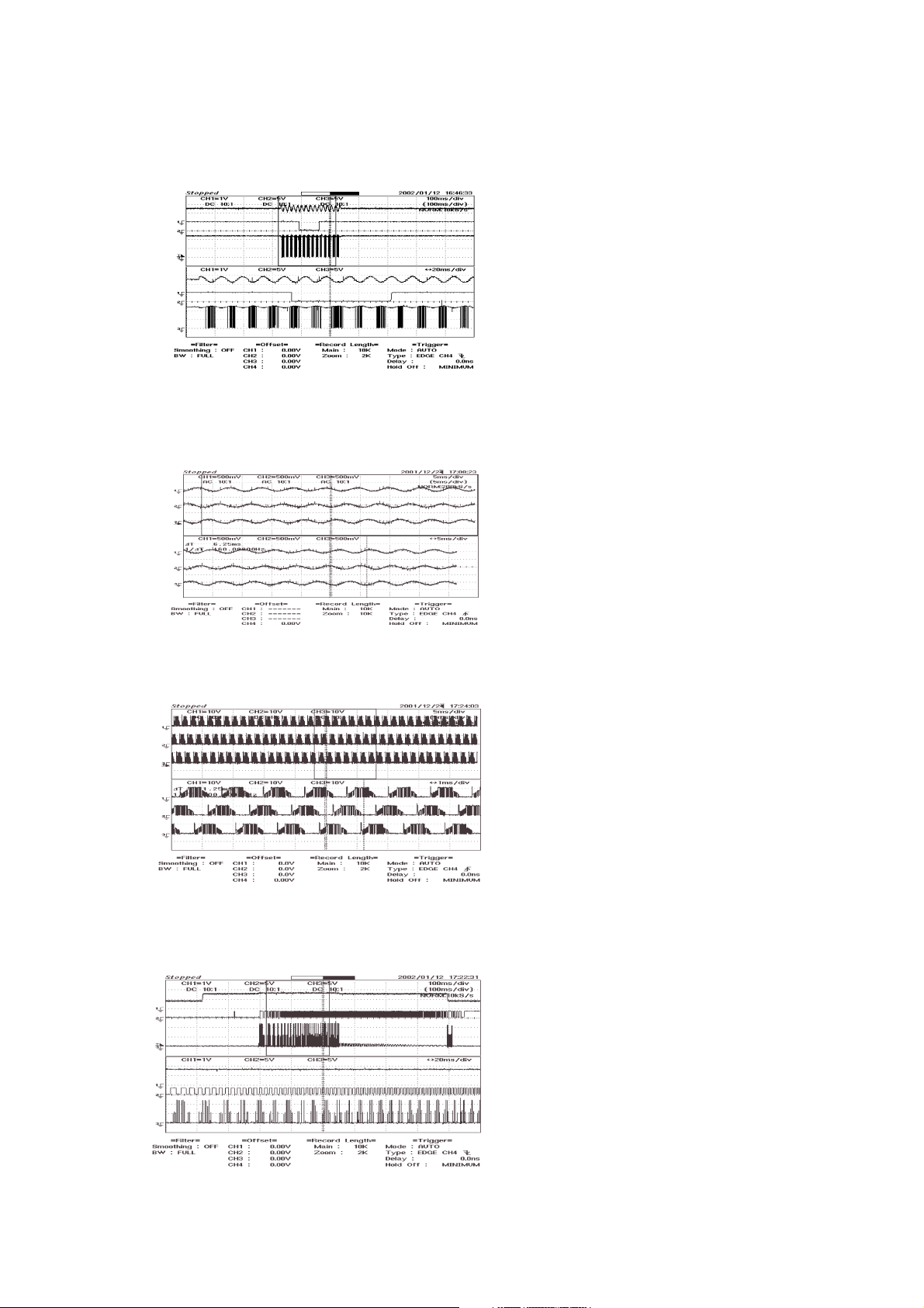
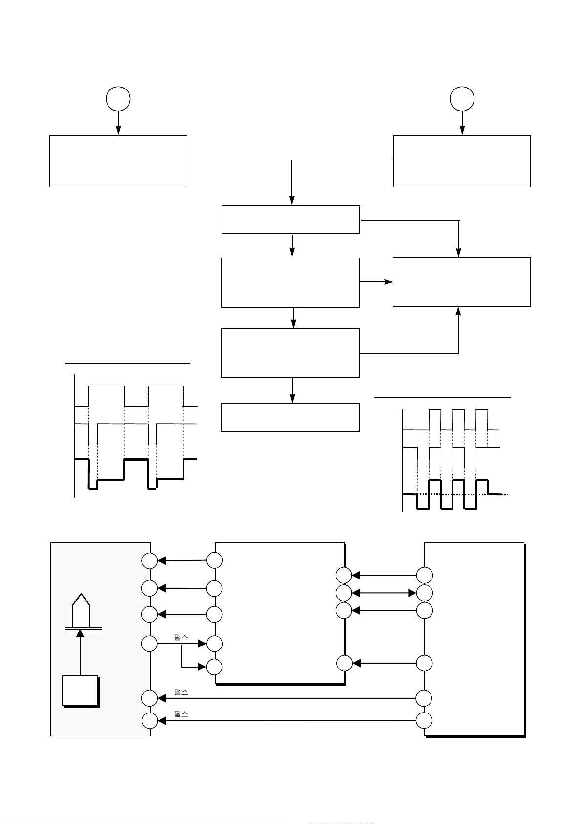
1. Waveform when Sled moves to inside
SLIN1
/SLEDINSW
A+
2. Waveform of Spindle rotation
HU+
HV+
HW+
3. Waveform of Spindle Kick
SPIN
FG
U
Zoom in
wave
Zoom in
wave
Zoom in
wave
Zoom in
wave
When the sled moves to the inner position,
the sine wave(refer to Fig1) inputs to
SLIN1/SLIN2 (the input pins of drive IC).
When Pick-Up unit approached to innermost
position, the /SLEDINSW signal(CN402 pin 1)
becomes 0 V.
The output pins A+ ,A-, B+, B- of the drive IC is
PWM waveform and drives the Stepping Motor.
The output signal of Hall(HU+, HU-, HV+, HV,
HW+, HW-) comes from a Hall sensor of spindle
motor and they were inputted to pin 1, 2, 3, 4, 5, 6
of drive IC(BD7907FS) via CN402. When spindle
motor rotate, HU+, HW+, HV+ signals are
generated in a regular order with 120
0
phase delay
each other.(Refer Fig 2)
If waveforms of HU+, HU-, HV+, HV-, HW+, HWdifferent from Fig 2, check the pin 7(HB signal) of
drive IC. The HB signal must be about 5V.
Wave of U,V,W assigned to pin 9,11,18 of Drive
IC is a PWM waveform and they drive Spindle
motor.
When spindle motor rotate, U/W/V signals are
generated in a regular order with 120
0
phase delay
each other. (Refer Fig 3)
If waveforms different from Fig 3, check pin
27(VC), pin 51(VCC), pin22(CTL1), pin23 (CTL2),
R514, R512, R510, R511.
When spindle kick, refer to Fig 4.
Fig.1
Fig.2
Fig.3
Fig.4
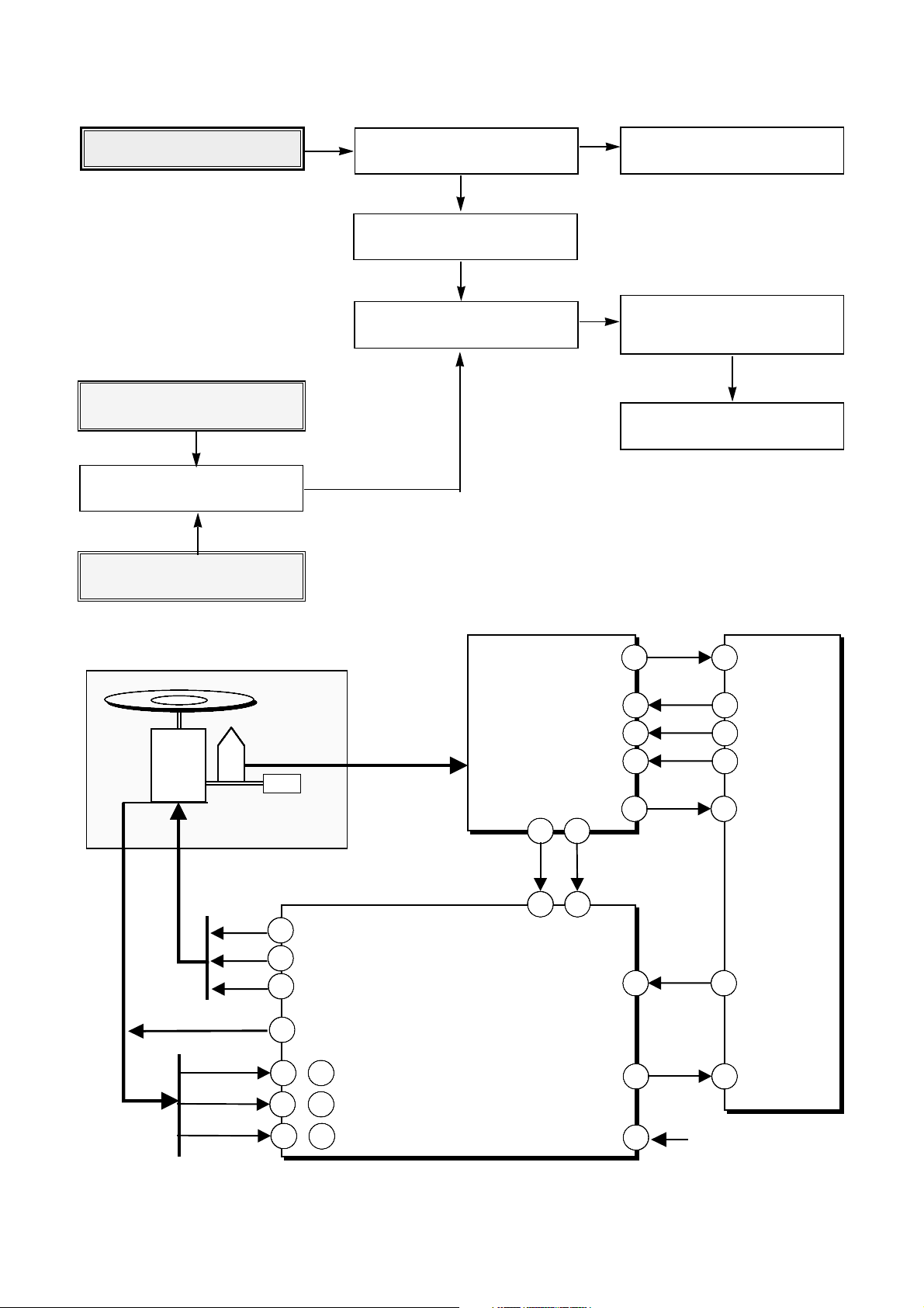
56
Check Tray operation.
Check /EJECT KEY
(pin 11 of IC101).
Check the output signal of tray
(pin 49, 50 of IC501).
Check the LED.
Check operating signal of tray
(pin 26 of IC501).
• Check the control singal of Drive IC
(pin 22, 23 of IC501).
• Check the power of DRIVE IC and
VC.
Check operating signal of LED (pin
96, 98 of IC401).
Check SCLK, SDATA, XLAT (pin
122, 123, 124 of IC401).
Check operation S/W of tray
(/OPEN SW:pin 94 of IC401
/LOAD SW : pin 95 of IC401).
MT1518
LED102
LED101
Q802
Q801
SW103
DETECTOR
-TRAY
2
1
LED1
96
IC 401
LED2
98
MT1516
RF Amp
/OPEN_SW
/LOAD_SW
General port use
94
95
101
102
122
123
124
SCLK
SDATA
XLA T
65
63
62
IC 101
MT1508
FRONT
SW102
EJECT
-SW
Tray Motor
M
TRAY -
TRAY +
DRV-MUTE2 DRV-MUTE1
23
22
49
CTL1
CTL2
LDIN
BD7907FS
6Ch Servo DRIVE
27
50
IC 501
VC
/EJECT_KEY
PWMOUT
1.4 V
2426
Processor
11
DSP
Decoder
Encoder
I / F
Micro
57
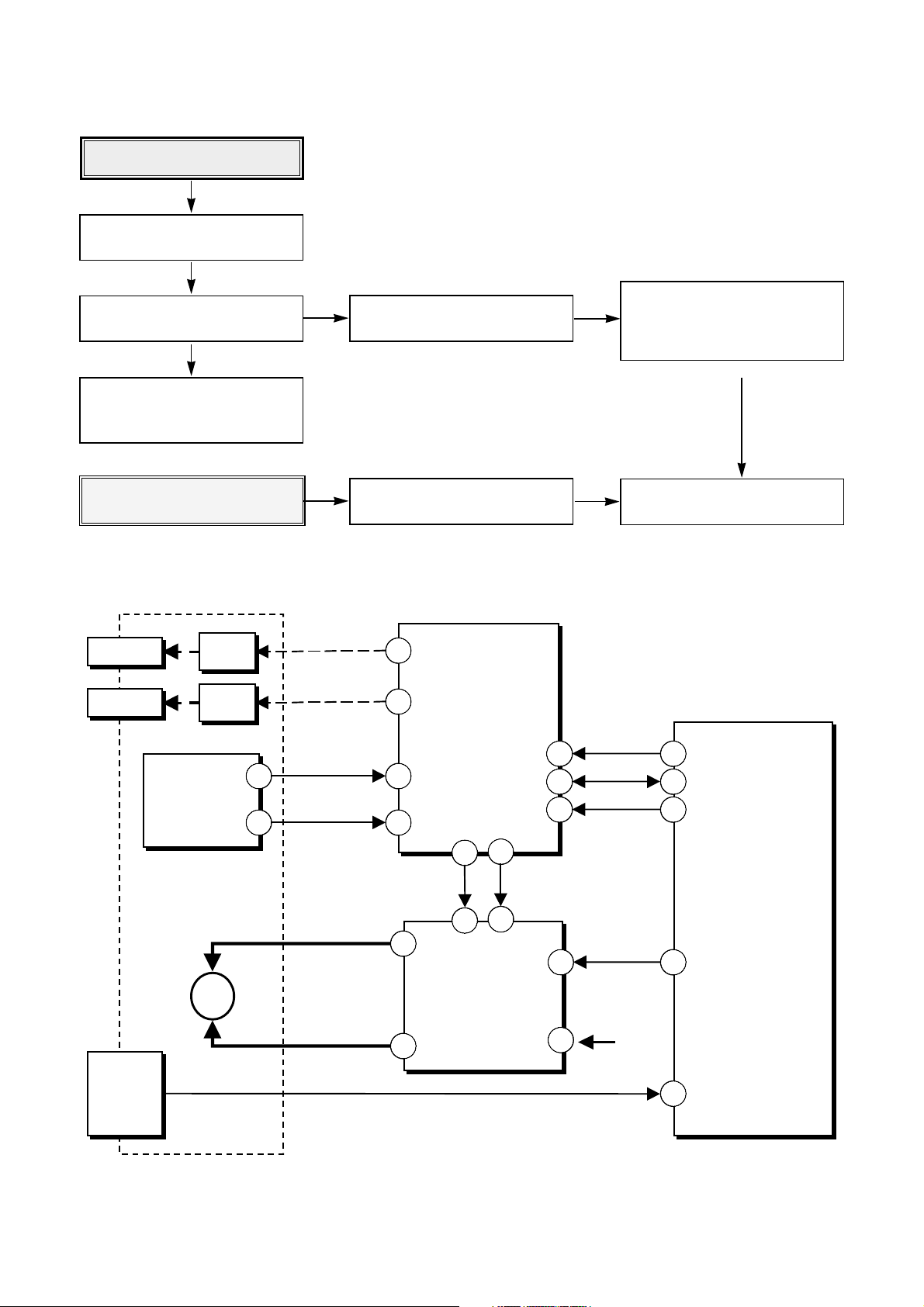
Check identification of Drive.
Check the connection of ATAPI
cable.
Check the communication between
PC and MT1518 (IC101).
Check SDRAM.
(IC102)
Check Flash ROM
(IC103).
2. Connection of Power and ATAPI cable
MT1508
DSP
Decoder
Encoder
ATIP Demodulator
Write Strategy
Write S/H Signal
I / F
Micro Processor
H
O
S
T
8MB
SDRAM
I/F
cable
Address
Data
IC 101
IC 103
IC 102
AT49F002N
512KB
Flash ROM
33.868 8MHz
74 75
Address
Data
Pin no. Pin name Pin no. Pin name
39 DASP GND 40
37 CS1 CS3 38
35 DA0 DA2 36
33 DA1 PDIAG 34
31 INTRQ IO16 32
29 DMACK GND 30
27 IORDY CSEL 28
25 IOR GND 26
23 IOW GND 24
21 DMARQ GND 22
19 GND KEY 20
17 HD0 HD15 18
15 HD1 HD14 16
13 HD2 HD13 14
11 HD3 HD12 12
9 HD4 HD11 10
7 HD5 HD10 8
5 HD6 HD9 6
3 HD7 HD8 4
1 /HRST GND 2
CN101(ATAPI)
SDRAM
MT1518
AT49F040
58
Check the identification of CD-
ROM Disc (insert Disc).
Check the operation of Focus.
Check the operation of Tracking.
Check the Jump action.
• Check the drive signal of FCS-/+
(pin 1, 2 of CN201).
• Check drive input signal of Focus
(pin 53 of IC501 : FCIN).
• Check the input signal of FE
(pin 42 of IC101 : FEI).
• Check the input signal of SBAD
(pin 38 of IC101).
• Check the input signal of CSI (pin
41 of IC401).
• Check the input signal of RFZC (pin
60 of IC101 : HRFZC).
• Check the drive signal of TRK+/(pin 3, 4 of CN201).
• Check the signal of Tracking
(pin 52 of IC501 : TKIN).
• Check the signal of SLED
(pin 28, 29 of IC501 : SLIN1, 2).
• Check control signal of Drive IC
(pin 22, 23 of IC501: CTL1,2).
• Check power and VC of DRIVE IC.
Check signal of A~H (pin 39, 38, 37,
36, 30, 31, 32, 33 of IC401).
Check the input signal of TE
(pin 40 of IC101 : TEI).
In case of Focus Up/Down
MT1516
RF Amp
General port use
IC 401
123
124
122
SCLK
SDATA
XLA T
MT1518
DSP
Decoder
Encoder
I / F
Micro Processor
IC 101
63
62
65
BD7907FS
6Ch Servo
DRIVE
IC 501
DRV-MUTE2
DRV-MUTE1
CTL2
CTL1
27
1.4 V
VC
45
TEO
40
43
CSI
41
49
SBAD
38
NJM
3404
7
IC 505
1
52
53
6
2
23
22
Optical
Pick-up
KRS-340B
45 46
1 2
47 48
3 4
FCS-
FCS+
TRK+
TRK-
22
23
101
102
FCIN
TKIN
FOO
TRO
FOSO
TRSO
A ~ D
E ~ H
CN 201
TEI
CSI
SBAD
42
FEO
42
FEI
FMO
29
SLI N2
28
SLI N1
27
26
FMO2
126
RFZC
60
HRFZC
59
4. Operation of Focus Up/Down
FE
SBAD
FCS+
5. Waveform of Track Following
6. Waveform of Track Jump
TE
EQRF
CE
SLIN1
7. Waveform of Spindle Servo On
SPIN
FG
U
Zoom in
wave
Focus Search
Focus Servo On
Zoom in
wave
Zoom in
wave
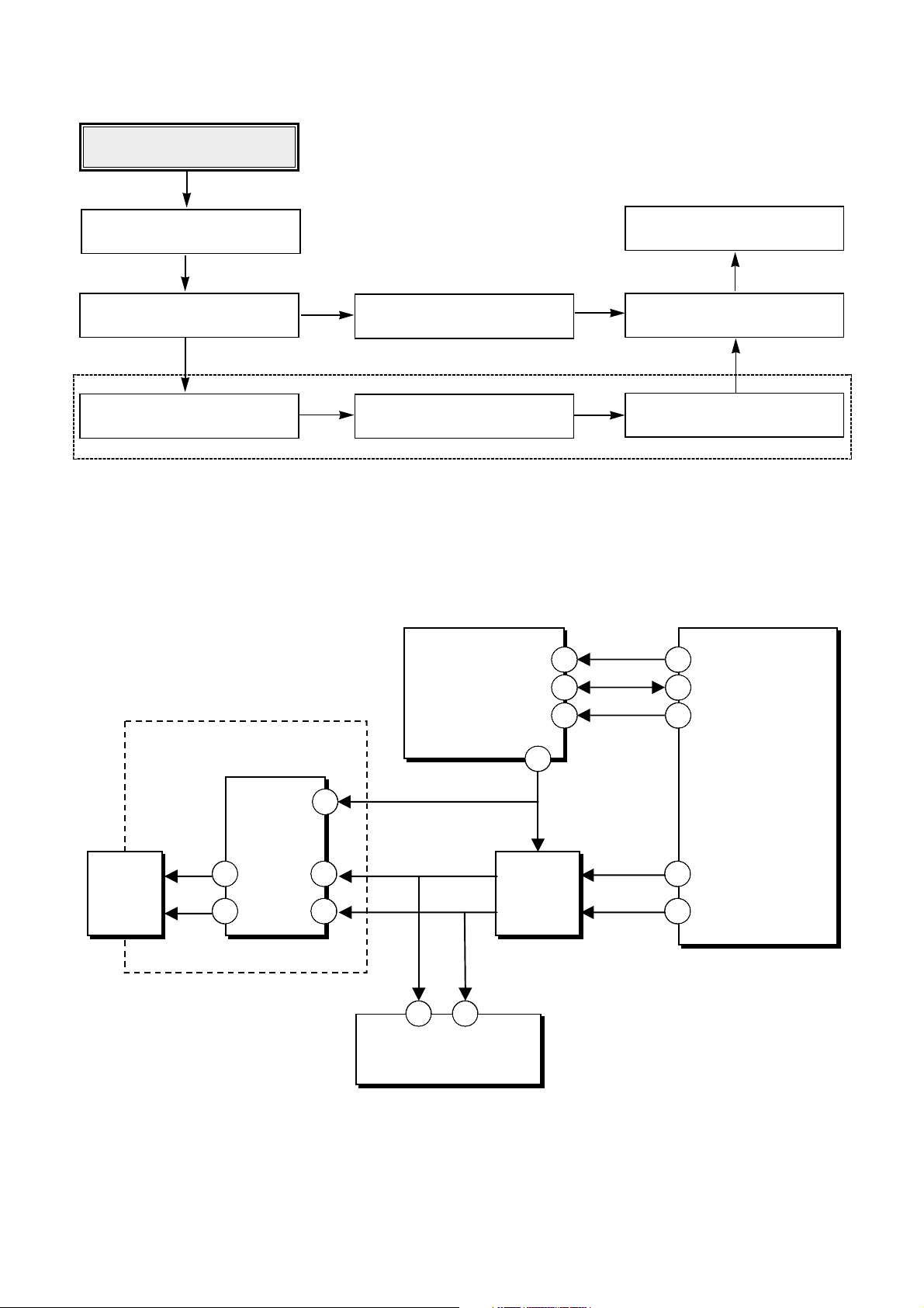
Waveform of Focus Search refer to Fig 5.
In Focus Search, FE signal and SBAD signal are
used to Focus Servo On.
Therefore, in case of Focusing Fail, check the FE
signal and SBAD signal.
Waveform of Track Following(Sequential Read)
refer to Fig 6.
By Sled Servo, SLIN1, SLIN2 (pin 28, 29 of Drive
IC) drive the Sled Motor(Stepping Motor) for
locating the lens on the center axis of Pick-up.
Waveform of Track Jump refer to Fig 7.
Center level of TE,CE is 1.4V.
SLIN1, SLIN2 signal (pin 28, 29 of Drive IC)
assume the form of Pulse. And they drive the Sled
Motor(Stepping Motor).
RFZC(RF Ripple Zero Cross) signal is Pulse form
and it lags behind TE signal 90
0
.
To maintain constant rpm(CAV) or linear
velocity(CLV), the drives control spindle motor.
The Fig 8 shows the waveforms when spindle
servo is on.
TE
RFZC
CE
SLIN1
Fig.5
Fig.6
Fig.7
Fig.8
60
Check RF and Spindle
(Insert CD-ROM Disc).
Check the identification of
CD-R Disc(Insert Blank CD-R).
Check the identification of CD-RW
Disc (Insert Blank CD-R).
Check EQRF input signal
(pin 45 of IC101)
Check the signal of A~H (pin 39, 38,
37, 36, 30, 31, 32, 33, of IC401)
Check the operation signal of Spindle
(pin 24 of IC501).
Check SCLK, SDATA, XLAT
(pin 122, 123, 124 of IC401).
Check FG input
(pin 20 of IC101).
Check the input signal of ATFG
(pin 69 of IC101).
• Check the control signal of Drive IC
(pin 22, 23, of IC501).
• Check power/VC of DRIVE IC.
Spindle
Motor
Optical
Pick-up
KRS-340B
STEP Motor
A ~ D
E ~ H
DRV-MUTE2 DRV-MUTE1
IC 401
MT1516
RF Amp
Wobble
General port use
102101
EQRF
21
122
123
124
SCLK
SDATA
XLA T
45
65
63
62
IC 101
MT1518
ATFG
116 69
DSP
Decoder
Encoder
I / F
HB
HU+ , HU-
HV+ , HV-
HW+ , HW-
23
U
9
V
11
W
18
IC 501
22
CTL1
CTL2
SPIN
2524
ATIP
Demodulator
DMO
Micro
7
Processor
BD7907FS
21
,
4
3
,
65
,
6Ch Servo
DRIVE
FG
VC
27
1.4 V
2021
FG
61
Check point of Writing
Check the compatibility between
Drive and Tool.
Check Disc state (Fingerprint,
Scratch, Dust...).
Check whether or not additional
writing is allowed.
(Given in the Disc Info of writing tool)
Check whether or not Disc is
writeable (CD-R/CD-RW).
(ALPC initial value before ‘Laser Power Setting’)
MT1518
Check Laser 1
(Check EEPROM)
Activate ‘Addition Func.’ window in
Test Tool(GGOOM6).
Execute ‘S/N’ (Identify Serial
Number).
Execute ‘ALPC Parameters’
(Identify ALPC Parameters).
Check the communication line
of EEPROM.
Execute ‘C. Laser Power
setting’ in Test Tool(GGOOM6).
Check whether or not ‘ALPC
Parameters is initial value.
CS
IC 203
SLK
AT93C86
2KB
EEPROM
DI
DO
1
2
3
4
110
108
107
EEP-SDATA
EEP-CS
EEP-CL K
MT1516
IC 401
ALPC
EEPROM access
IC 101
MT1508
Decoder
Encoder
122
123
124
SCLK
SDATA
XLA T
65
63
62
Micro
Processor
NG
NG
OK
62
Check Laser 2 (No disc).
Execute ‘E.ALPC Test for AS’ in
Test Tool (GGOOM6) (select
‘VRDC Loop’, and ‘Trigger’).
E
E
Check Read Laser
Initial value of FPDO : 2.8V +/- 10%.
OFF LEVEL.
VRDC LEVEL FPD.
Execute ‘D. Laser Inspection’ in
Test Tool (GGOOM6).
Check the input of ENBL
(pin 33 of CN201 : ‘H’).
Check the input of VRDC
(pin 25 of CN201 : 0.4~0.8V).
Check the input of FPDO (pin 54,
65 of IC401 : FPDO~0.1V).
• Check the input of RLDON
(pin 128 of IC401 : ‘H’).
• Check SCLK, SDATA, XLAT
(pin 122, 123, 124 of IC401).
Check Reference voltage.
NG
F
NG
G
VWDC1 LEVEL FPD.
VWDC2 FPD.
MT1516
ALPC
MT1518
Decoder
Encoder
Write Strategy
Write S/H Signal
Micro
Processor
IC 101CN 201
5
ENBL
IC 401
Optical
Pick-up
KRS-340B
LD
Drive
33
0.4~0.8 V
19FPDO 54
65
FPDO
FPDOLP
ENBL
FPDO-0.1V
123
124
122
63
62
65
SCLK
SDATA
XLAT
6325
VRDCO
VRDC
128 57
RLDON
H
H
63
Execute ‘E.ALPC Test for AS’ in
Test Tool(GGOOM6) (Select
‘CD-R Rec Mode’, and ‘Trigger’)
F
Inspection of CD-R Recording Laser
Execute ‘E. ALPC Test for AS’ in
Test Tool (GGOOM6) (Select
‘CD-RW Rec Mode’, and
‘Trigger’)
G
Inspection of CD-RW writing Laser
Chect input of ENBL
(pin 33 of CN201 : ‘H’).
• Check input of VWDC1
(pin 26 of CN201 : 0.4~1.0V).
• Check input of VWDC2
(pin 27 of CN201 : 0.1~0.5V).
• Check input of WLDON
(pin 27 of IC401 : ‘H‘)
• Check SCLK, SDATA, XLAT
(pin 122, 123, 124 of IC401)
• Check input of WXR
(pin 30 of CN201 : Pulse)
• Check input of ODON
(pin 31 of CN201 : Pulse)
Check input of FPDO
(pin 54, 65 of IC401 : Pulse).
Initial value of FPDO :
2.8V/-10%)
CD-R Recording Pulse
WXR
CD-RW Recording Pulse
ODON
FPDO
Optical
Pick-up
KRS-340B
Drive
CN 201
LD
ENBL
VWDC1
VWDC2
WXR
33
26
19FPDO 54
H
0.4~1.0 V
62
0.1~0.5 V
6127
65
5
ENBL
VWDC1O
VWDC2O
IC 401
MT1516
ALPC
FPDO
FPDOLP
WLDON
WXR
ODON
FPDO
122
123
124
127 58
SCLK
SDATA
XLAT
H
65
63
62
1330
IC 101
MT1518
Decoder
Encoder
Write Strategy
Write S/H Signal
Micro
Processor
WXR
ODON
31
15
ODON
64
Check Audio signal
(Insert Audio Disc).
Identify playback of Audio Disc
(Play Mode).
Check Output signal of AUIO L/R
(pin 51, 54 of CN100).
Check Output signal of AUDIO
L/R (pin 165, 167 of IC101).
Check Output signal of
/AUD-MUTE (pin 103 of IC401).
Check SCLK, SDATA, XLAT
(pin 122, 123, 124 of IC401).
Check Output signal of AUDIO
L/R (pin 1, 7 of IC801).
Check Input signal of AUDIO L/R
(pin 3, 5 of IC801).
Check Input signal of
/AUD-MUTE (pin 3 of IC801).
Output of Headphone
MT1516
RF Amp
General p
ort use
MT1508
DSP
Decoder
Encoder
I / F
Micro Processor
IC 101
BH3544F
AUDIO
AMP
IC 801
103
IC 401
LO
165
RO
167
AUDIO Line Out
51 54
CN 100
JK101
H-JACK
SB
3
5
3
Audio
Mute
Circuit
1
7
123
124
122
63
62
65
SCLK
SDATA
XLAT
L-CH R-CH
ROUT
LOUT
ROUT
LOUT
/AUD-MUTE
ROUT
LOUT
MUTE
FRONT
MT1518
65
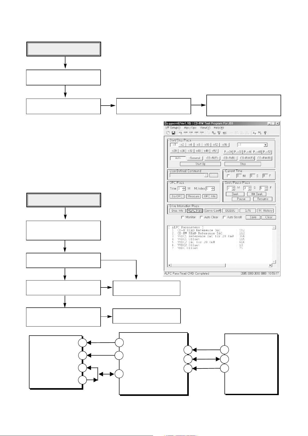
A. Start
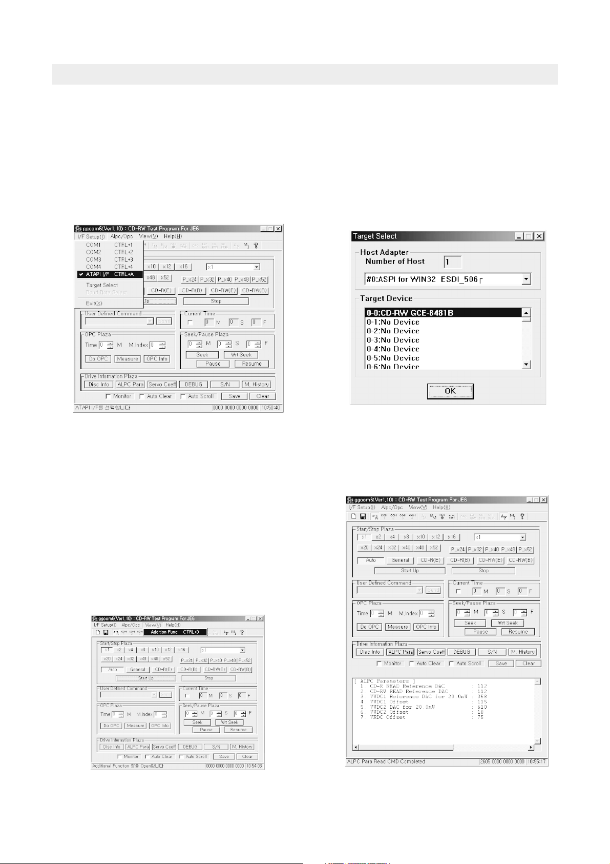
1. Install GCE-8481B -> PC Power ON -> Execute Windows.
2. Execute GGOOM6.exe on Windows (GGOOM6.exe & GGOOM6.cfg should be on the same Directory).
3. If you use GCE-8481B, “GGOOM6(Ver x.xx)” will be displayed on the Window Frame.
4. Select I/F Setup on the menu bar.
5. Select ATAPI I/F and then Click OK.
6. Select Target Select on the menu bar.
7. Select Number of Host(#0 or #1) appropriately, then “GCE-8481B” displays on Target Device.
8. Select “GCE-8481B” on Target Device, and then Click OK.
B. Check ALPC Parameters
1. Select VIEW on the menu bar.
2. Click Addition Func. on VIEW window -> New frame will be displayed.
3. Click ALPC Para tab.
[ALPC Parameters]
1) CD-R READ Reference DAC : 60 ~185
2) CD-RW READ Reference DAC : 60 ~185
3) VWDC1 : 200 ~ 296
4) VWDC1 Offset : 30 ~ 175
5) VWDC2 : 499 ~787
6) VWDC2 Offset : -55 ~ 75
4. Close Calibration window.
• How to use Test Tool (GGOOM6)
[I/F Setup Menu]
[Target Select window]
[ALPC Parameters Menu]
[Additional Function Menu]
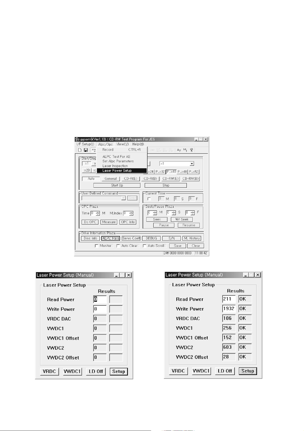
C. Laser Power Setup (VWDC / VWDC 1, 2 re-setup)
1. Remove disc on the tray.
2. Select ALPC/OPC on the menu bar, and then select Laser Power Setup menu.
3. Setup LD Power meter (Frequency :780nm, Measure Range : 0.01mW unit).
4. Click VRDC button on the Laser Power Setup window. Laser beam will be emitted from LD.
5. Measure LD Power with LD Power meter. Type the result in the blank(Read Power box).
[Ex] 2.11mW ->211
6. Click VWDC1 button and follow above step 5. But VWDC1 result should be filled in the Write Power box.
[Ex] 19.32mW ->1932
7. Click Setup button, and result will be displayed with OK or NG.
8. Close Laser Power Setup window.
66
[Laser Power Setup window]
[Laser Power Setup Frame]
[Laser Power Setup Result]
 Loading...