

Page 1

3
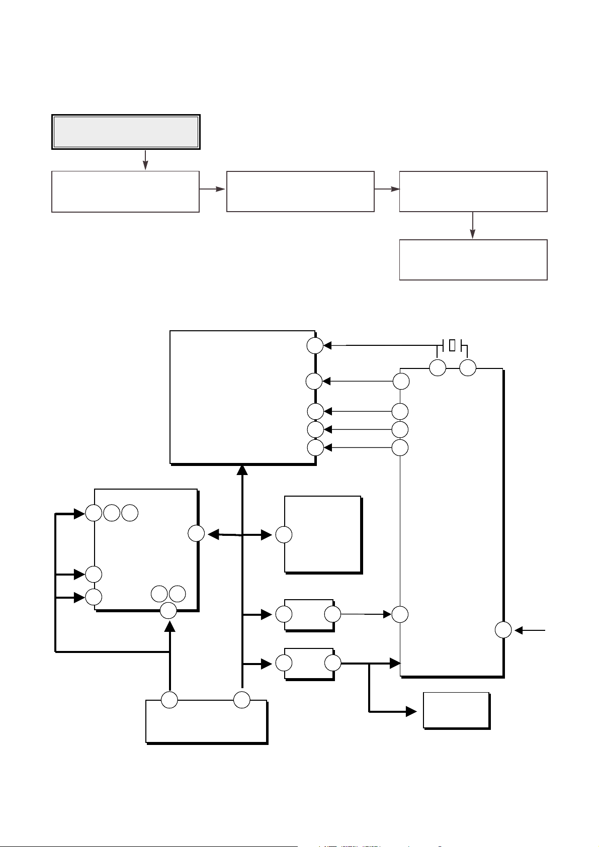
INTRODUCTION
FEATURES
1. General
1) Enhanced IDE interface.
2) Internal 5.25 inch, halfheight CD-R/RW Drive.
3) 8 Mbytes (or 2Mbytes) buffer memory.
4) Audio CD like tray loading of a disc without using a caddy.
5) Power loading and power ejecting of a disc. The disc can also be ejected manually.
6) Supports Power saving mode and Sleep mode.
7) Vertical and Horizontal operation.
8) SuperLink Function.
2. Supported disc formats
1) Reads and writes data in each CD-ROM, CD-ROMXA, CD-I FMV, Video CD, and CD-EXTRA
2) Reads data in Photo CD (Single and Multi session).
3) Reads and writes standard CD-DA.
4) Reads and writes CD-R discs conforming to “Orange Book Part 2”.
5) Reads and writes CD-RW discs conforming to “Orange Book Parts 3”.
3. Supported write method
1) Disc at once (DAO), Session at once (SAO), Track at once (TAO), Variable packet, Fixed packet, and
Multi-session.
4. Performance
1) Random 100 ms average access time.
2) CD-R Record speed : 8X, 12X, 16X, 20X~40X (PCAV).
3) CD-RW Record speed : 4X, 10X, 12X.
4) CD-ROM : Max 6,000 KB/s(Max 40x) Sustained Transfer rate.
5) Supports real time error correction and real time layered error correction at each speed.
6) PIO Mode 4, Multi DMA Mode 2 .
7) Multimedia MPC-3 Spec compliant.
8) Support CD-TEXT read/write.
5. Audio
1) Output 16 bit digital data over ATA interface.
2) 8 Times Digital Filter for CD Audio
3) Software Volume Control
4) Equipped with audio line output and headphone jack for audio CD playback.
5) Front panel Volume Control for Headphone Output.
This service manual provides a variety of service
information.
It contains the mechanical structure of the CDR/RW Drive and the electronic circuits in
schematic form. This CD-R/RW Drive was
manufactured and assembled under our strict
quality control standards and meets or exceeds
industry specifications and standards.
This CD-R/RW drive is an internal drive unit
designed for use with IBM PC, HP Vectra, or
compatible computer. It can write as much as 700
Mbytes of digital data into CD-R/RW disc, and can
read as much as 650 Mbytes of digital data stored
in a CD-ROM, CD-R and CD-RW disc.
This CD-R/RW Drive can easily meet the
upcoming MPC level 3 specification, and its
Enhanced Intelligent Device Electronics (E-IDE)
and ATAPI interface allows Plug and play
integration in the majority of today’s PCs without
the need of an additional interface card.
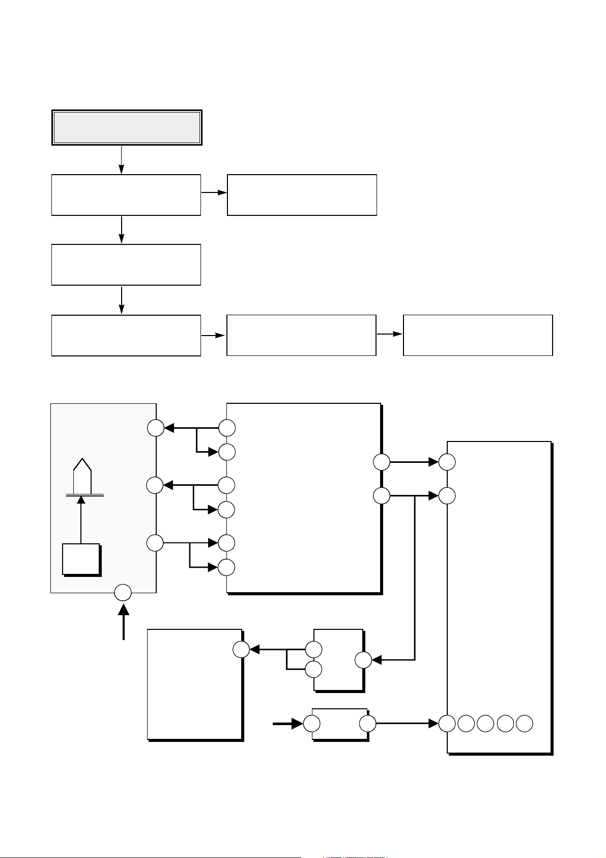
Page 2
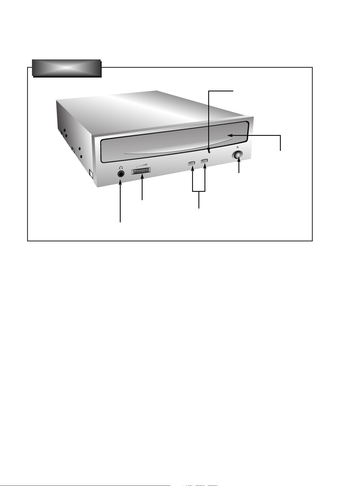
LOCATION OF CUSTOMER CONTROLS
6
1. Disc tray
This is the tray for the disc. Place the disc on the
ejected disc tray, then lightly push the tray (or
push the eject button) and the CD will be loaded.
NOTE: Don’t pull out or push in the disc tray
forcibly. This might cause damage to the loading
section of the drive.
2. Stop/Eject button
This button is pressed to open the CD tray.
This button works only when power is supplied to
the drive.
If an Audio CD is playing, pressing this button will
stop it, and pressing it again will open the tray.
3. Emergency Eject Hole
Insert a paper clip here to eject the Disc tray
manually or when there is no power.
4. Volume control
This is used to adjust the output volume of the
headphone jack. It can’t be used to adjust the
output volume for the audio output connectors on
the rear panel.
NOTE : Turn the volume down before turning on
the power. Sudden loud noises can damage your
hearing.
5. Headphone jack
This jack is for connecting headphones or minispeakers.
6. Drive activity indicators
Two colored LEDs are used to indicate the
operation of CD-R/RW Drive.
(1) Read
The orange color is displayed when the spindle
motor begins the Spin up operation: accessing
data, reading data, playing Audio, and up loading
tray.
(2) Write
The green color is flashed during disc writing
sessions.
READ
READ
WRITE
WRITE
Headphone Jack
Volume
Control
Drive Activity Indicators
Stop/Eject Button
Disc Tray
Emergency Eject Hole
Front Panel
Page 3
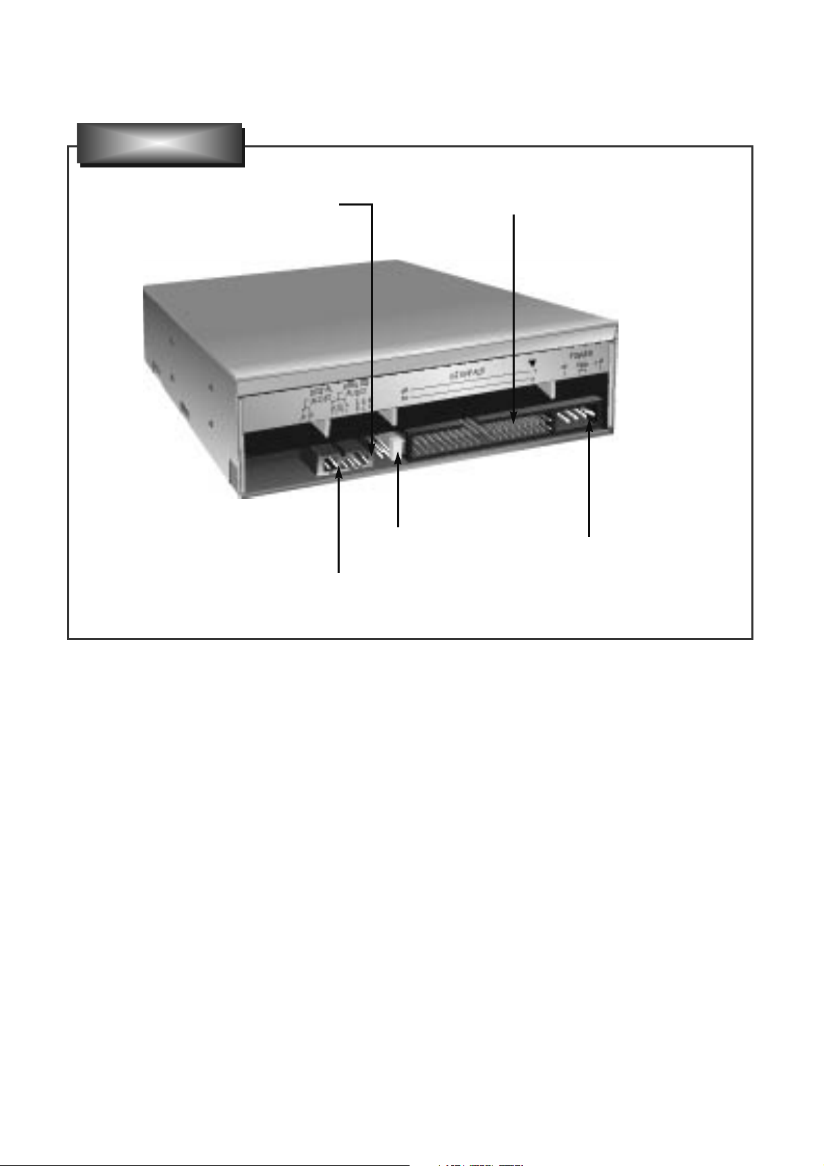
7
1. Power Connector
Connects to the power supply (5-and 12-V DC) of
the host computer.
NOTE : Be careful to connect with the proper
polarity. Connecting the wrong way may damage
the system (and is not guaranteed). Usually this
connector can only be attached one-way.
2. IDE Interface Connector
Connect to the IDE (Integrated Device
Electronics) Interface using a 40-pin flat IDE
cable.
NOTE : Do not connect or disconnect the cable
when the power is on, as this could cause a short
circuit and damage the system. Always turn the
power OFF when connecting or disconnecting the
cable.
3. Jumper Connector
This jumper determines whether the drive is
configured as a master or slave. Changing the
master-slave configuration takes effect after
power-on reset.
4. Analog Audio Output Connector
Provides output to a sound card (analog signal).
Generally you need this to play a regular audio
CD.
5. Digital Audio Output Connector
Provides output to a sound card (digital signal).
Digital Audio Output
Connector
Jumper Connector
Analog Audio Output Connector
IDE Interface Connector
Power Connector
Rear Panel
Page 4
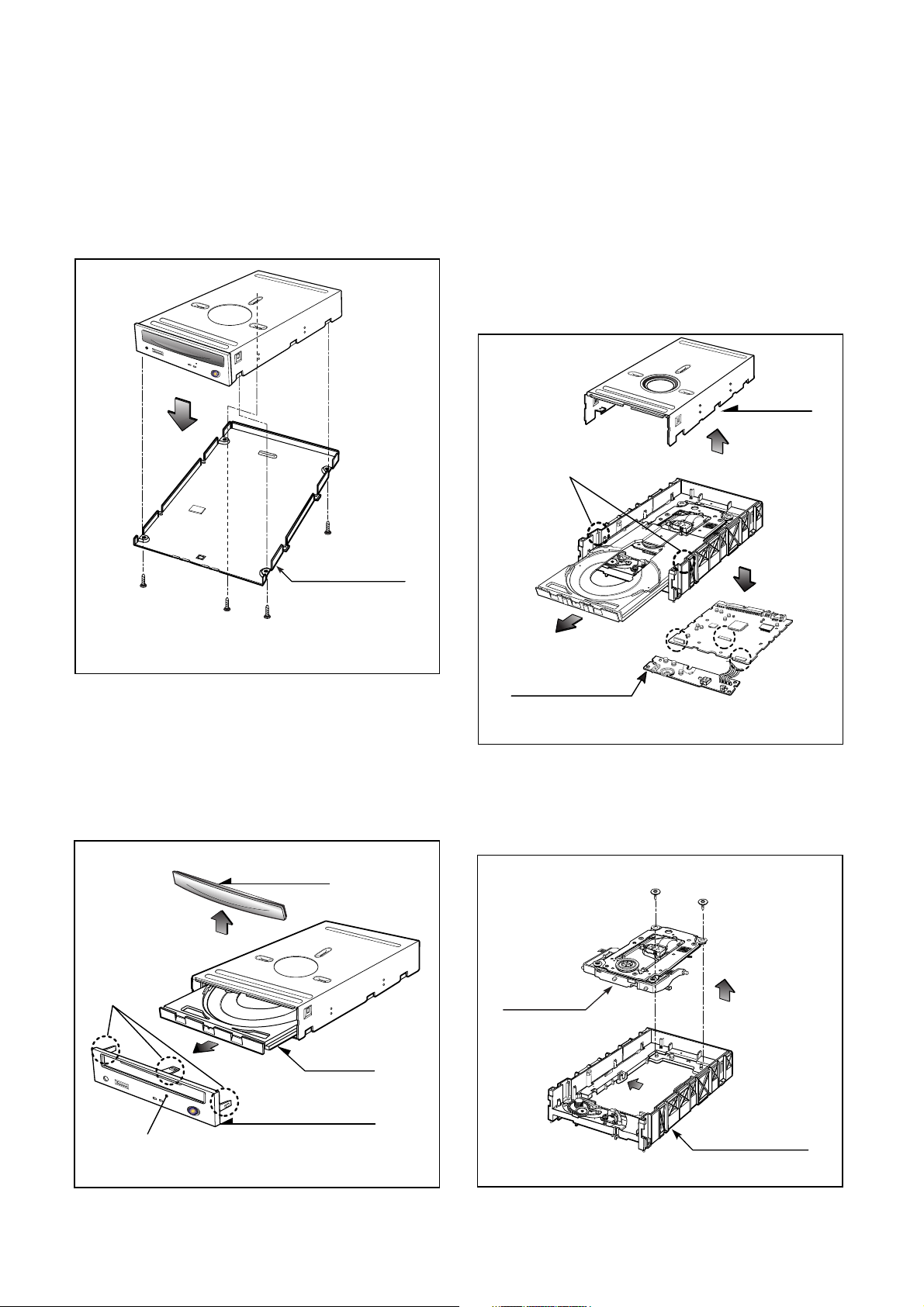
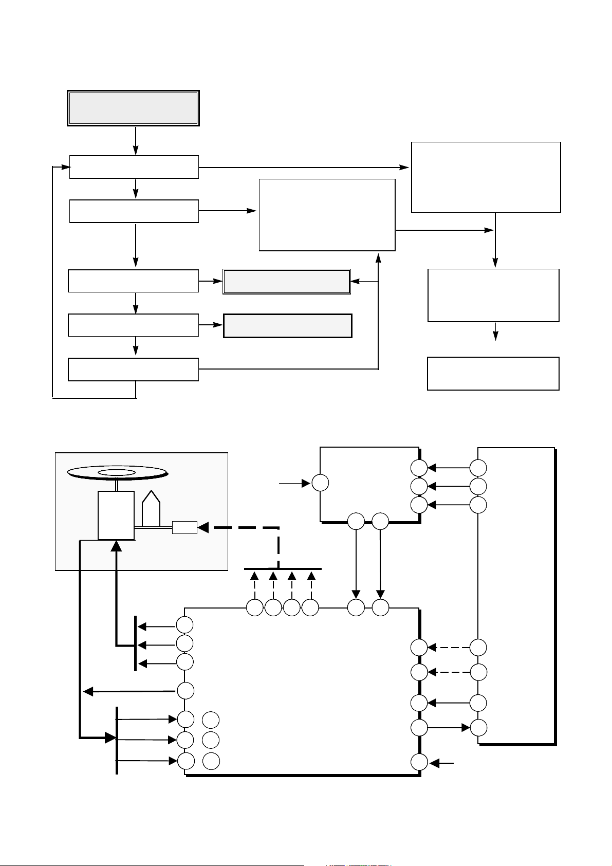
1. CABINET and CIRCUIT BOARD
DISASSEMBLY
1-1. Bottom Chassis
A. Release 4 screws (A) and remove the Bottom Chassis
in the direction of arrow (1). (See Fig.1-1)
1-2. Front Bezel Assy
A. Insert and press a rod in the Emergency Eject
Hole and then the CD Tray will open in the direction
of arrow (2).
B. Remove the Tray Door in the direction of arrow
(3) by pushing the stoppers forward.
C. Release 3 stoppers and remove the Front Bezel Assy.
1-3. Cabinet and Main Circuit Board
A. Remove the Cabinet in the direction of arrow (4).
(See Fig. 1-3)
B. Release 2 hooks (a) and remove the CD Tray
drawing forward.
C. Remove the Main Circuit Board in the direction of
arrow (5).
D. At this time, be careful not to damage the 4
connectors, are positioned at right side, of the Main
Circuit Board.
2. MECHANISM ASSY DISASSEMBLY
2-1. Pick-up Unit
A. Release screws (B).
B. Separate the Pick-up Unit in the direction of arrow (6).
(4)
(5)
Main
Circuit Board
Cabinet
Hooks (a)
Fig. 1-1
Fig. 1-2
DISASSEMBLY
8
Fig. 1-3
Mechanism Assy
Pick-up Unit
(6)
(B)
(B)
Fig. 2-1
(1)
(A)
Bottom Chassis
(A)
(A)
(A)
(3)
Stoppers
Emergency Eject Hole
(2)
Tray Door
Front Bezel Assy
CD Tray
Page 5
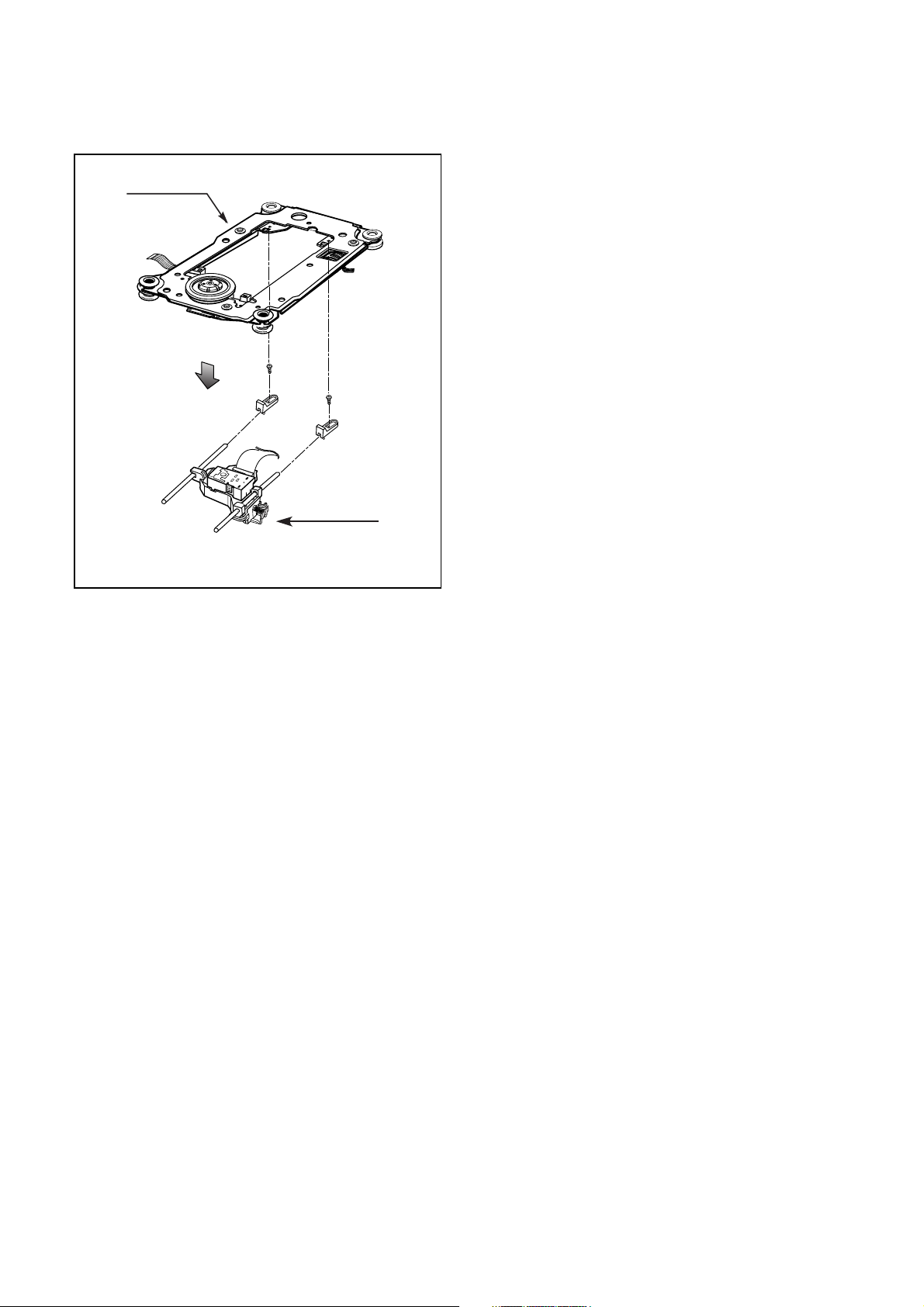
2-2. Pick-up
A. Release 2 screws (C) and remove the Pick-up.
Pick-up Unit
Pick-up
(C)
(C)
Fig. 2-2
9
Page 6
TROUBLESHOOTING GUIDE
Power check
(Malfunction of LED and Tray)
55
Check the connection of 5V, 12V.
Check the Reset (Pin 170, 122 of
IC101, pin2 of IC401)
Check the input of oscillation (pin
109 of IC401)
Check SCLK, SDATA, XLAT
(pin 122, 123, 124 of IC401)
1. Connect only the power cable
BD7907FS
6Ch Servo DRIVE
MT1516
RF Amp
Wobble
ALPC
General port use
EEPROM access
MT1508
DSP
Decoder
Encoder
ATIP Demodulator
Write Strategy
Write S/H Signal
I / F
Micro Processor
33.868 8MHz
IC 101
IC 501
IC 103
IC 401
IC 102
3.3 V
Reset
12V 5V
AT49F002N
512KB
Flash ROM
IC 502
41
109
44
2
54
31
3
32
10 19 20
31
32
30
44 51
IC 202
2 170
PRST
‘ L ’
122
/ HRST
‘ H ’
74 75
MCLK
55
‘ H ’
/XRST
SDRAM
123
124
122
63
62
65
SCLK
SDATA
XLAT
CN 100
Page 7
56
Check the Reference voltage
(+/- 10%)
Check VC (1.4V) of Drive IC
(pin27 of IC501)
Check voltage of VREF(1.4V)
(pin 53 of IC101, pin 27 of IC501)
Check voltage of 2VREF(2.8V)
(pin 52 of IC101)
Check HAVC/PDVC(2.0V)
(pin 34 of IC401, pin 13 of CN201)
Check FVREF/FPDVC (2.8V)
(pin 52 of IC401, pin22 of CN201)
Check FPDO(2.8V)
(pin 54, 65 of IC401)
CN 201
Optical
Pick-up
KRS-330B
FPDVC
FPDO
LD
Drive
FPDVcc
20
5 V
PDVC
13
22
19
6Ch Servo DRIVE
2.0 V
2.8 V
2.8V
IC 501
VC
BD7907FS
75
VHAVC
34
HAVC
MT1516
74
52
54
65
VFVREF
FVREF
FPDO
FPDOLP
27
RF Amp
Wobble
ALPC
General port use
EEPROM access
1.4 V
IC 401
IC 506
1
2
NJM
3414
V28
V14
IC 101
2.8 V
76
1.4 V
76
52
53
2VREF
VREF
MT1508
DSP
Decoder
Encoder
ATIP Demodulator
Write Strategy
Write S/H Signal
I / F
3
Micro Processor
3.3 V
2.5 V
IC 503
32
17 28 76 134 18 0
Page 8
57
Check the initial operation
(Power-on state)
• Check the operating signal of Sled
(pin 28, 29 of IC501 : SLIN1, 2)
• Check the output signal of Sled
(pin 34, 35, 36, 37 of IC501)
• Check /SLEDIN_SW.
(pin 104 of IC401)
• Check the control signal of Driver
IC(pin 22, 23 of IC501)
• Check the power of DRIVE IC
and VC
Check SCLK, SDATA, XLAT
(pin 122, 123, 124 of IC401)
Sled move to inside
Spindle motor rotate
Laser On
Check the Laser
•
Check the Spindle signal
(pin 24 of IC501 : SPIN)
•
Check FG input
(pin 20 of IC101)
•
Check the Hall signal
(pin 1, 2, 3, 4, 5, 6 of IC501)
Check the operation of Focus
Focus up / Down
Laser Off / Spindle Stop
2 times iteration
Spindle
Motor
HB
HU+ , HU-
HV+ , HV-
HW+ , HW-
Optical
Pick-up
KRS-330B
STEP Motor
U
9
V
11
W
18
7
1
3
(From pin 1 of CN402)
/SLEDIN_SW
34
B+ A- A+
B-
373635
IC 501
BD7907FS
2
,
4
,
65
,
6Ch Servo
DRIVE
IC 401
MT1516
104
ALPC
General port use
DRV-MUTE2
22
CTL1
102101
23
CTL2
SCLK
122
SDATA
123
XLA T
124
DRV-MUTE1
65
63
62
Processor
SLIN1
SLIN2
SPIN
FG
VC
28
29
27
26
27
2524
2021
1.4 V
IC 101
MT1508
DSP
I / F
Micro
FMO
FMO2
DMO
FG
Page 9
58
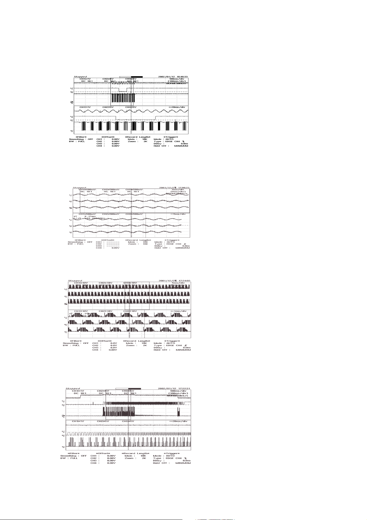
1. Waveform when Sled moves to inside
SLIN1
/SLEDINSW
A+
2. Waveform of Spindle rotation
HU+
HV+
HW+
3. Waveform of Spindle Kick
SPIN
FG
U
Zoom in
wave
Zoom in
wave
Zoom in
wave
Zoom in
wave
When the sled moves to the inner position,
the sine wave(refer to Fig1) inputs to
SLIN1/SLIN2 (the input pins of drive IC).
When Pick-Up unit approached to innermost
position, the /SLEDINSW signal(CN402 pin 1)
becomes 0 V.
The output pins A+ ,A-, B+, B- of the drive IC is
PWM waveform and drives the Stepping Motor.
The output signal of Hall(HU+, HU-, HV+, HV,
HW+, HW-) comes from a Hall sensor of spindle
motor and they were inputted to pin 1, 2, 3, 4, 5, 6
of drive IC(BD7907FS) via CN402. When spindle
motor rotate, HU+, HW+, HV+ signals are
generated in a regular order with 120
0
phase delay
each other.(Refer Fig 2)
If waveforms of HU+, HU-, HV+, HV-, HW+, HWdifferent from Fig 2, check the pin 7(HB signal) of
drive IC. The HB signal must be about 5V.
Wave of U,V,W assigned to pin 9,11,18 of Drive
IC is a PWM waveform and they drive Spindle
motor.
When spindle motor rotate, U/W/V signals are
generated in a regular order with 120
0
phase delay
each other. (Refer Fig 3)
If waveforms different from Fig 3, check pin
27(VC), pin 51(VCC), pin22(CTL1), pin23 (CTL2),
R514, R512, R510, R511.
When spindle kick, refer to Fig 4.
Fig.1
Fig.2
Fig.3
Fig.4
Page 10
59
Check Tray operation
Check /EJECT KEY
(pin 11 of IC101)
Check the output signal of tray
(pin 49, 50 of IC501)
Check the LED
Check operating signal of tray
(pin 26 of IC501)
• Check the control singal of Drive IC
(pin 22, 23 of IC501)
• Check the power of DRIVE IC and
VC
Check operating signal of LED (pin
96, 98 of IC401)
Check SCLK, SDATA, XLAT (pin
122, 123, 124 of IC401)
Check operation S/W of tray
(/OPEN SW:pin 94 of IC401
/LOAD SW : pin 95 of IC401)
LED102
LED101
Q802
Q801
SW103
DETECTOR
-TRAY
2
1
LED1
96
IC 401
LED2
98
MT1516
RF Amp
/OPEN_SW
/LOAD_SW
General port use
94
95
101
102
122
123
124
SCLK
SDATA
XLA T
65
63
62
IC 101
MT1508
FRONT
SW102
EJECT
-SW
Tray Motor
M
TRAY -
TRAY +
DRV-MUTE2 DRV-MUTE1
23
22
49
CTL1
CTL2
LDIN
BD7907FS
6Ch Servo DRIVE
27
50
IC 501
VC
/EJECT_KEY
PWMOUT
1.4 V
DSP
Decoder
Encoder
I / F
2426
Micro
Processor
11
Page 11
60
Check identification of Drive
Check the connection of ATAPI
cable
Check the communication between
PC and MT1508 (IC101)
Check SDRAM
(IC102)
Check Flash ROM
(IC103)
2. Connection of Power and ATAPI cable
MT1508
DSP
Decoder
Encoder
ATIP Demodulator
Write Strategy
Write S/H Signal
I / F
Micro Processor
H
O
S
T
8MB
SDRAM
I/F
cable
Address
Data
IC 101
IC 103
IC 102
AT49F002N
512KB
Flash ROM
33.868 8MHz
74 75
Address
Data
Pin no. Pin name Pin no. Pin name
39 DASP GND 40
37 CS1 CS3 38
35 DA0 DA2 36
33 DA1 PDIAG 34
31 INTRQ IO16 32
29 DMACK GND 30
27 IORDY CSEL 28
25 IOR GND 26
23 IOW GND 24
21 DMARQ GND 22
19 GND KEY 20
17 HD0 HD15 18
15 HD1 HD14 16
13 HD2 HD13 14
11 HD3 HD12 12
9 HD4 HD11 10
7 HD5 HD10 8
5 HD6 HD9 6
3 HD7 HD8 4
1 /HRST GND 2
CN101(ATAPI)
SDRAM
Page 12
61
Check the identification of CD-
ROM Disc (insert Disc)
Check the operation of Focus
Check the operation of Tracking
Check the Jump action
• Check the drive signal of FCS-/+
(pin 1, 2 of CN201)
• Check drive input signal of Focus
(pin 53 of IC501 : FCIN)
• Check the input signal of FE
(pin 42 of IC101 : FEI)
• Check the input signal of SBAD
(pin 38 of IC101)
• Check the input signal of CSI (pin
41 of IC401)
• Check the input signal of RFZC (pin
60 of IC101 : HRFZC)
• Check the drive signal of TRK+/(pin 3, 4 of CN201)
• Check the signal of Tracking
(pin 52 of IC501 : TKIN)
• Check the signal of SLED
(pin 28, 29 of IC501 : SLIN1, 2)
• Check control signal of Drive IC
(pin 22, 23 of IC501: CTL1,2)
• Check power and VC of DRIVE IC
Check signal of A~H (pin 39, 38, 37,
36, 30, 31, 32, 33 of IC401)
Check the input signal of TE
(pin 40 of IC101 : TEI)
In case of Focus Up/Down
MT1516
RF Amp
General port use
IC 401
123
124
122
SCLK
SDATA
XLA T
MT1508
DSP
Decoder
Encoder
I / F
Micro Processor
IC 101
63
62
65
BD7907FS
6Ch Servo
DRIVE
IC 501
DRV-MUTE2
DRV-MUTE1
CTL2
CTL1
27
1.4 V
VC
45
TEO
40
43
CSI
41
49
SBAD
38
NJM
3404
7
IC 505
1
52
53
6
2
23
22
Optical
Pick-up
KRS-330B
45 46
1 2
47 48
3 4
FCS-
FCS+
TRK+
TRK-
22
23
101
102
FCIN
TKIN
FOO
TRO
FOSO
TRSO
A ~ D
E ~ H
CN 201
TEI
CSI
SBAD
42
FEO
42
FEI
FMO
29
SLI N2
28
SLI N1
27
26
FMO2
126
RFZC
60
HRFZC
Page 13

62
4. Operation of Focus Up/Down
FE
SBAD
FCS+
5. Waveform of Track Following
6. Waveform of Track Jump
TE
EQRF
CE
SLIN1
7. Waveform of Spindle Servo On
SPIN
FG
U
Zoom in
wave
Focus Search
Focus Servo On
Zoom in
wave
Zoom in
wave
Waveform of Focus Search refer to Fig 5.
In Focus Search, FE signal and SBAD signal are
used to Focus Servo On.
Therefore, in case of Focusing Fail, check the FE
signal and SBAD signal.
Waveform of Track Following(Sequential Read)
refer to Fig 6.
By Sled Servo, SLIN1, SLIN2 (pin 28, 29 of Drive
IC) drive the Sled Motor(Stepping Motor) for
locating the lens on the center axis of Pick-up.
Waveform of Track Jump refer to Fig 7.
Center level of TE,CE is 1.4V.
SLIN1, SLIN2 signal (pin 28, 29 of Drive IC)
assume the form of Pulse. And they drive the Sled
Motor(Stepping Motor).
RFZC(RF Ripple Zero Cross) signal is Pulse form
and it lags behind TE signal 90
0
.
To maintain constant rpm(CAV) or linear
velocity(CLV), the drives control spindle motor.
The Fig 8 shows the waveforms when spindle
servo is on.
TE
RFZC
CE
SLIN1
Fig.5
Fig.6
Fig.7
Fig.8
Page 14

63
Check RF and Spindle
(Insert CD-ROM Disc)
Check the identification of
CD-R Disc(Insert Blank CD-R)
Check the identification of CD-RW
Disc (Insert Blank CD-R)
Check EQRF input signal
(pin 45 of IC101)
Check the signal of A~H (pin 39, 38,
37, 36, 30, 31, 32, 33, of IC401)
Check the operation signal of Spindle
(pin 24 of IC501)
Check SCLK, SDATA, XLAT
(pin 122, 123, 124 of IC401)
Check FG input
(pin 20 of IC101)
Check the input signal of ATFG
(pin 69 of IC101)
• Check the control signal of Drive IC
(pin 22, 23, of IC501)
• Check power/VC of DRIVE IC
Spindle
Motor
Optical
Pick-up
KRS-330B
STEP Motor
A ~ D
E ~ H
DRV-MUTE2 DRV-MUTE1
IC 401
MT1516
RF Amp
Wobble
General port use
102101
EQRF
21
122
123
124
SCLK
SDATA
XLA T
45
65
63
62
IC 101
MT1508
ATFG
116 69
DSP
Decoder
Encoder
I / F
HB
HU+ , HU-
HV+ , HV-
HW+ , HW-
23
U
9
V
11
W
18
IC 501
22
CTL1
CTL2
SPIN
ATIP
Demodulator
2524
DMO
Micro
7
Processor
BD7907FS
21
,
4
3
,
65
,
6Ch Servo
DRIVE
FG
VC
27
1.4 V
2021
FG
Page 15

64
Check point of Writing
Check the compatibility between
Drive and Tool
Check Disc state (Fingerprint,
Scratch, Dust...)
Check whether or not additional
writing is allowed.
(Given in the Disc Info of writing tool)
Check Laser 1
(Check EEPROM)
Activate ‘Addition Func.’ window in
Test Tool(GGOOM4)
Execute ‘S/N’ (Identify Serial
Number)
Execute ‘ALPC Parameters’
(Identify ALPC Parameters)
Check the communication line of
EEPROM
Execute ‘C. Laser Power setting’ in
Test Tool(GGOOM4)
Check whether or not ‘ALPC
Parameters is initial value
Check whether or not Disc is
writeable (CD-R/CD-RW)
(ALPC initial value before ‘Laser Power Setting’)
IC 203
AT93C86
2KB
EEPROM
CS
SLK
DI
DO
IC 101
1
2
3
4
110
EEP-CS
108
EEP-CL K
MT1516
107
EEP-SDATA
ALPC
EEPROM access
IC 401
122
123
124
SCLK
SDATA
XLA T
65
63
62
Processor
MT1508
Decoder
Encoder
Micro
Page 16

NG
NG
OK
65
Check Laser 2 (No disc)
Execute ‘E.ALPC Test for AS’ in
Test Tool (GGOOM4) (select
‘VRDC Loop’, and ‘Trigger’)
E
E
Check Read Laser
Initial value of FPDO : 2.8V +/- 10%
OFF LEVEL
VRDC LEVEL FPD
Execute ‘D. Laser Inspection’ in
Test Tool (GGOOM4)
Check the input of ENBL
(pin 33 of CN201 : ‘H’)
Check the input of VRDC
(pin 25 of CN201 : 0.4~0.8V)
Check the input of FPDO (pin 54,
65 of IC401 : FPDO~0.1V)
• Check the input of RLDON
(pin 128 of IC401 : ‘H’)
• Check SCLK, SDATA, XLAT
(pin 122, 123, 124 of IC401)
Check Reference voltage
NG
F
NG
G
VWDC1 LEVEL FPD
VWDC2 FPD
MT1516
ALPC
MT1508
Decoder
Encoder
Write Strategy
Write S/H Signal
Micro
Processor
IC 101CN 201
5
ENBL
IC 401
Optical
Pick-up
KRS-330B
LD
Drive
33
0.4~0.8 V
19FPDO 54
65
FPDO
FPDOLP
ENBL
FPDO-0.1V
123
124
122
63
62
65
SCLK
SDATA
XLAT
6325
VRDCO
VRDC
128 57
RLDON
H
H
Page 17

66
Execute ‘E.ALPC Test for AS’ in
Test Tool(GGOOM4) (Select
‘CD-R Rec Mode’, and ‘Trigger’)
F
Inspection of CD-R Recording Laser
Execute ‘E. ALPC Test for AS’ in
Test Tool (GGOOM4) (Select
‘CD-RW Rec Mode’, and
‘Trigger’)
G
Inspection of CD-RW writing Laser
Chect input of ENBL
(pin 33 of CN201 : ‘H’)
• Check input of VWDC1
(pin 26 of CN201 : 0.4~1.0V)
• Check input of VWDC2
(pin 27 of CN201 : 0.1~0.5V)
• Check input of WLDON
(pin 27 of IC401 : ‘H‘)
• Check SCLK, SDATA, XLAT
(pin 122, 123, 124 of IC401)
• Check input of WXR
(pin 30 of CN201 : Pulse)
• Check input of ODON
(pin 31 of CN201 : Pulse)
Check input of FPDO
(pin 54, 65 of IC401 : Pulse)
Initial value of FPDO :
2.8V/-10%)
CD-R Recording Pulse
WXR
CD-RW Recording Pulse
ODON
FPDO
Optical
Pick-up
KRS-330B
Drive
CN 201
LD
ENBL
VWDC1
VWDC2
WXR
33
26
19FPDO 54
H
0.4~1.0 V
62
0.1~0.5 V
6127
65
5
ENBL
VWDC1O
VWDC2O
IC 401
MT1516
ALPC
FPDO
FPDOLP
WLDON
WXR
ODON
FPDO
122
123
124
127 58
SCLK
SDATA
XLAT
H
IC 101
65
63
62
MT1508
Decoder
Encoder
Write Strategy
Write S/H Signal
Micro
Processor
1330
WXR
ODON
31
15
ODON
Page 18

67
Check Audio signal
(Insert Audio Disc)
Identify playback of Audio Disc
(Play Mode)
Check Output signal of AUIO L/R
(pin 51, 54 of CN100)
Check Output signal of AUDIO
L/R (pin 165, 167 of IC101)
Check Output signal of
/AUD-MUTE (pin 103 of IC401)
Check SCLK, SDATA, XLAT
(pin 122, 123, 124 of IC401)
Check Output signal of AUDIO
L/R (pin 1, 7 of IC801)
Check Input signal of AUDIO L/R
(pin 3, 5 of IC801)
Check Input signal of
/AUD-MUTE (pin 3 of IC801)
Output of Headphone
MT1516
RF Amp
General p
ort use
MT1508
DSP
Decoder
Encoder
I / F
Micro Processor
IC 101
BH3544F
AUDIO
AMP
IC 801
103
IC 401
LO
165
RO
167
AUDIO Line Out
51 54
CN 100
JK101
H-JACK
SB
3
5
3
Audio
Mute
Circuit
1
7
123
124
122
63
62
65
SCLK
SDATA
XLAT
L-CH R-CH
ROUT
LOUT
ROUT
LOUT
/AUD-MUTE
ROUT
LOUT
MUTE
FRONT
Page 19

68
A. Start
1. Install GCE-8400B -> PC Power ON -> Execute Windows.
2. Execute GGOOM4.exe on Windows (GGOOM4.exe & GGOOM.cfg should be on the same Directory).
3. If you use GCE-8400B, “GGOOM4(Ver x.xx)” will be displayed on the Window Frame.
4. Select I/F Setup on the menu bar.
5. Select ATAPI I/F and then Click OK.
6. Select Target Select on the menu bar.
7. Select Number of Host(#0 or #1) appropriately, then “GCE-8400B” displays on Target Device.
8. Select “GCE-8400B” on Target Device, and then Click OK.
B. Check ALPC Parameters
1. Select VIEW on the menu bar.
2. Click Addition Func. on VIEW window -> New frame will be displayed.
3. Click ALPC Para tab.
[ALPC Parameters]
1) CD-R READ Reference DAC : 50 ~143
2) CD-RW READ Reference DAC : 50 ~143
3) VWDC1 - VWDC1 Offset : 105 ~ 160
4) VWDC1 Offset : 30 ~ 165
5) VWDC2 - VWDC2 Offset : 190 ~ 384
6) VWDC2 Offset : -45 ~ 75
4. Close Calibration window.
• How to use Test Tool (GGOOM4)
[I/F Setup Menu]
[Target Select window]
[ALPC Parameters Menu]
[Additional Function Menu]
Page 20

C. Laser Power Setup (VWDC1 / VWDC2 re-setup)
1. Remove disc on the tray.
2. Select ALPC/OPC on the menu bar, and then select Laser Power Setup menu.
3. Setup LD Power meter (Frequency :780nm, Measure Range : 0.01mW unit).
4. Click VRDC button on the Laser Power Setup window. Laser beam will be emitted from LD.
5. Measure LD Power with LD Power meter. Type the result in the blank(Read Power box).
(If you don’t have LD Power meter, type the written value on pickup without decimal point including two
digits under the decimal point.)
[Ex] 11.34mW ->1134
6. Click VWDC1 button and follow above step 5. But VWDC1 result should be filled in the Write Power box.
7. Click Setup button, and result will be displayed with OK or NG.
8. Close Laser Power Setup window.
69
[Laser Power Setup window]
[Laser Power Setup Frame]
[Laser Power Setup Result]
Page 21

70
[Laser Inspection]
[Laser Power Test Frame]
[Laser Power Test Result]
D. Laser Inspection (VRDC/VWDC/FPD Level check)
1. Remove disc on the Tray.
2. Select ALPC/OPC on the menu bar and select Laser Inspection menu, then Laser Power Test window
will appear.
3. Click Trigger button, then the result will be displayed with OK or NG separately.
4. Close Laser Power Test window.
Page 22

72
BD7907FS
6Ch Servo DRIVE
MT1516
RF Amp
Wobble
ALPC
General port use
EEPROM acce ss
MT1508
DSP
Decoder
Encoder
ATIP Demodulator
Write Strategy
Write S/H Signal
I / F
Micro Processor
Audio
Mute
Circuit
H
O
S
T
33.868MHz
Optical
Pick-up
KRS-330B
SDRAM
I/F
cable
Data
Address
STEP Motor
FCS
TRK
Spindle
Motor
Writing
Pulse
Servo S/H,
Write S/H Signal
Data, Clock, XLAT
Reset
Line Out
L,R
AT93C86
2KB
EEPROM
EQRF,
RRF,
FEI,TEI,CSI
DMO
FOO
TRO
SLO
Address/
Data
PWM out
F PD
ABCD
EFGH
IC 401
IC 101
IC 501
IC 103
IC 102
Audio
L,R
3.3 V
Reset
5V
12V
IC 203
AT49F002N
512KB
Flash ROM
LD
Drive
VWDC
VRDC
2.5 V
FG
M
Tray Motor
Drive Mute
LED Control
Mechanism S/W Detect
Functional Block Diagram
Page 23

MAJOR IC INTERNAL BLOCK DIAGRAM AND PIN DESCRIPTION
IC401 (MT1516) : CD-R/RW Analog Signal Processor
Block Diagram
39
APC
RFZC1
MCLK
DIG.
REG.
MPX1
MPX2
VCON
RRFX
ADBCO
BCO
ADO
FPDOX
TELP
MPPO
SPPO
DRCLP
RFRP
MPX1
TZC
MPX2
MPX1
ASH
BSH
DSH
ESH
CSH
FSH
GSH
HSH
MPX2
MPX2B
VWDC2O
VWDC1O
VRDCO
WREF1
VWDC1
VWDC1N
FPDOLP
FVREF
FPDO
RREF
VRDC
VRDCN
RFPDSH
WFPDSH
RLDON
WLDON
FPDOX
RRF
RRFX
EQRF
GAINUP
SERVSH
WBLSH
ADBCO
ADO
BCO
FEO
MPPO
SBADO
SPPO
S/H
&
MATRIX
ROPC
FE
DRCO2
CE
TE
SBAD
TEIN
RFZC
SHPC
RFZC1VC
SHBC
DEFECT
Data
Slicer
RECDIN
TE
FE
CE
SBADOLP
INA
INB
INC
IND
HAVC
INA
INB
INC
IND
HAVC
INA
INB
INC
IND
HAVC
EQRF
VCON
GAINUP
EQRF
RFSUM
MPXOUT1
VREFMPX
AVDD1
AVSS1
AVDD2
AVSS2
AVDD3
AVSS3
AVDD4
AVSS4
AVDD5
AVS S5
AVDD6
AVS S6
AVDD7
AVSS7
AVDD8
AVS S8
AVDD9
AVSS9
S DATA
XLAT
SCLK
DRCSO
DRCMO
SLPFN
SLPFP
XDEFM
DEFM
RRFXLP
H11T
INH
ING
INF
INE
DRCO
INA
HAVC
IND
INB
INC
TROPEN
TRAYOUT#
TRAYIN#
LED1
LED2
LIMIT#
FR
ENDM
MUTE
SB
DEVSEL
EEP_SDATA
EEP_SCLK
EEP_CS
ENBL
GIO1~GIO7
General
I/O
SUBGND
TRCLOSE
ATIP
10-Bit
ADC
SERVO
&
Detection
SBAD
ASPREQ
OSTCC
RFAGCC
EQBIAS
EQRF
ROPCC
ROPCO
AUX2
AUX3
AUX1
WRFSUM
RRF
WRF
RFZC1
TZC
Voltage
Ref & DAC
VDAC1
VDAC0
VREF
VFVREF
V14
VHAVC
V28
P/B
Detect
x1
MPXOUT2
MPX2B
XRST
DVSS2
DVDD2
DVSS1
DVDD1
SBADLP
RECDIN/RRFSUM
RRFXLP
RRF/WRF
ATFMX
FPDO
ROPCO
RFAGCC
FVREF
VRDCB
VWDC1B
WREF1
VRDCO
RREF
WRFSH
AUX1
AUX2
AUX3
VWDC1O
VWDC2O
VDAC0
ATFG
ATFM
AGC3C
AGC2C
AGC1C
WBLCLK
Page 24

40
• Pin Assignment
Pin
Numbers
Symbol Type Description
RF Signals & S/H Control Pulses
36 INA Analog Input Input of Main Beam Signal (A)
37 INB Analog Input Input of Main Beam Signal (B)
38 INC Analog Input Input of Main Beam Signal (C)
39 IND Analog Input Input of Main Beam Signal (D)
30 INE Analog Input Input of Side Beam Signal (E)
31 INF Analog Input Input of Side Beam Signal (F)
32 ING Analog Input Input of Side Beam Signal (G)
33 INH Analog Input Input of Side Beam Signal (H)
34 HAVC Analog Input Reference Vol tage Input of Main and Side Beams (2.0V)
120 SERVSH
Digital Input (TTL),
SMT
S/H Control Pulse of Main and Side Beam Signals
118 WBLSH
Digital Input (TTL),
SMT
S/H Control Pulse of Wobble Signal
Focus/Tracking Error & Servo Control Signals
40 DRCO Analog Output Output of Differential Radial Contrast (DRC) Signal
41 DRCO2 Analog Input Re-Input of Differential Radial Contrast (DRC) Signal
42 FE Analog Output Output of Focusing Error Signal
45 TE Analog Output Output of Tr acking Error Signal
43 CE Analog Output Output of Center Error Signal
49 SBAD Analog Output Output of SBAD Signal
44 TEIN Analog Input Input of Out-of-Track Detection Circuit
50 SBADLP Analog Input Input of SBAD Signal after LPF for DEFECT Detection
46 SHPC Analog Output External Capacitor Connection for Peak Hold of RFRP Signal
47 RFZC1VC Analog Output Reference Vo ltage for RFRP Peak/Bottom Hold
48 SHBC Analog Output External Capacitor Connection for Bottom Hold of RFRP Signal
126 RFZC
Digital Output
(TTL), 4 mA Driving
Output of RF Zero Crossing Binary Signal
EQRF (RF Equalizer Filter and Data Slicer) Circuit
19 RFSUM Analog Input Input of RF Summing Signal from PUH to EQRF Block
11 EQBIA
S Analog Output External Bias Connection for Circuits in EQRF Block
13 OSTCC Analog Output
External Capacitor Connection for Offset Cancellation Circuit of
Equalizer Output
16 RFAGCC Analog Output External Capacitor Connection for RF AGC in EQRF Block
21 RFOUT Analog Output Output of RF EFM Signal after Equalizer Filter
4 DEFM
Digital Output
(TTL), 6 mA Driving
Binary Output of EFM Signal after Slicing (Positive)
3 XDEFM
Digital Output
(TTL), 6 mA Driving
Binary Output of EFM Signal after Slicing (Negative)
8 SLPFP Analog Input Input ( ) of Auto Slicing Level
9 SLPFN Analog Input Input of Auto Slicing Level
RRF & ROPC (Running OPC) Related Signals
22
RECDIN/
RRFSUM
Analog Input
(1). Input of RF Signal for Recorded Area Detection
(2). Input of Read RF Summing Signal from PUH to RRF Block
70 RRFXLP Analog Output Low Pass Output of RRF Signal
Page 25

41
Pin
Numbers
Symbol
Type
Description
24 RRF/WRF Analog Output
(1). Output of Read RF (RRF) Signal
(2). Output of Write RF (W RF) Signal
26 WRFSUM Analog Input Input of Write RF (WRF) Summing Signal to ROPC Block
27 ROPCO Analog Output Output of Amplified B-Level of Write RF Signal
28 ROPCC Analog Input Vin(-) of Amplifier for Sampled B-Level of WRF Signal
125 H11T
Digital Input (TTL),
SMT
S/H Control Pulse of WRF Signal
ATIP (Absolute Time In Pre-groove)
81 AGC1C Analog Output External Capacitor Connection for AGC1 in ATIP Block
82 AGC2C Analog Output External Capacitor Connection for AGC2 in ATIP Block
83 AGC3C Analog Output External Capacitor Connection for AGC3 in ATIP Block
85 ATFM Analog Output Output of Analog Wobble Signal
116 ATFG
Digital Output
(TTL), 4mA Driving
Digital Output of Wobble Signal after Slicing
114 WBLCLK
Digital Input (TTL),
SMT
External Clock Input for Wobble BPF (SCF)
APC (Auto Power Control for Laser)
54 FPDO Analog Input Input of Laser Monitor Voltage
65 FPDOLP Analog Input Input of Laser Monitor Voltage after Low Pass Filtering
52 FVREF Analog Input Reference Voltage of APC Loops
128 RLDON Digital Input (TTL) Laser Diode Control for Read Mode
127 WLDON Digital Input (TTL) Laser Diode Control for W rite Mode
112 RFPDSH
Digital Input (TTL),
SMT
S/H Control Pulse for Read APC Mode
111 WFPDSH
Digital Input (TTL),
SMT
S/H Control Pulse for Write APC Mode
55 RREF Analog I/O
(1). Input of Power Setting Voltage for Read APC; (2). Output of
Read APC Reference Voltage Generated by Built -in DAC
59 VRDCN Analog Input Vin(-) of Midcourse Amplifier for Read APC Loop
58 VRDC Analog Output Midcourse Output of Laser Diode Controlling in Read Mode
63 VRDCO Analog Output Output Vo ltage of Laser Diode Controlling in Read APC
53 WREF1 Analog I/O
(1). Input of Power Setting Voltage for Write APC 1; (2). Output of
Write APC Reference Voltage Generated by Built-in DAC
57 VWDC1N Analog Input Vin(-) of Midcourse Amplifier for Write APC 1
56 VWDC1 Analog Output Midcourse Output of Laser Diode Controlling in Write APC
62 VWDC1O Analog Output Output Voltage of Laser Diode Controlling in Write APC
61 VWDC2O Analog Output Output Voltage 2 of Laser Diode Controlling in Write APC
Reference Voltages & DACs
75 VHAVC Analog Output Output of Voltage Reference (2.0V)
78 VREF Analog Output Output of Voltage Reference (2.0V)
77 V14 Analog Output Output of Voltage Reference (1.4V)
76 V28 Analog Output Output of Voltage Reference (2.8V)
74 VFVREF Analog Output Output of Voltage Reference (2.5V~3.0V)
69 VDAC0 Analog I/O Output of General Purposed 8-Bit DAC (0V ~ 2.0V)
51 VDAC1 Analog Output Output of General Purposed 10-Bit DAC (0V ~ 4V)
MPXOUT (Multiplexer Circuit for Various Signals) and Testing Interface
68 AUX1 Analog Input Auxiliary Input 1 for Signal Monitoring
67 AUX2 Analog Input Auxiliary Input 2 for Signal Monitoring
66 AUX3 Analog Input Auxiliary Input 3 for Signal Monitoring
Page 26

42
Pin
Numbers
Symbol
Type
Description
71 MPXOUT1 Analog Output Multiplexer Output 1 for Signal Monitoring
72 MPXOUT2 Analog Output Multiplexer Output 2 for Signal Monitoring
Serial Interface & Other Digital Control Signals
1 ASPREQ
Digital Output
(TTL), 4 mA Driving
ASP request signal output to MT1508 to send control signals via
serial interface.
122 SCLK
Digital Input (TTL),
SMT
Clock Input for Register Setting
123 SDATA
Digital I/O (TTL),
4 mA Driving
Data Input/Output for Register Setting
124 XLAT
Digital Input (TTL),
SMT
Latch Input for Register Setting
2 XRST
Digital Input (TTL),
SMT
Digital Input for Register Resetting
109 MCLK
Digital Input (TTL),
SMT
Digital Input of Main Clock
95 TRAYIN#
Digital Input (TTL),
50K Pull-Up, SMT
Tr
n Input, A Logical Low Indicates the Tr ay is IN. Feedback
Flag from Tray Connector.
94 TRAYOUT#
Digital Input (TTL),
50K Pull-Up, SMT
Tr
Input. A Logical Low Indicates the Tr ay is OUT.
Feedback Flag from Tray Connector.
99 LIMIT#
Digital Input (TTL),
50K Pull-Up, SMT
Sledge Inner Limit Input, Active Low.
106 DEVSEL
Digital Input (TTL),
50K Pull-Up, SMT
Device Select. Cleared to ZERO Indicates the Driver is Master
Device. Set to ONE Indicates the Driver is Slave Device.
100 FR
Digital Input (TTL),
SMT
Spindle Motor Reverse Detection Input.
93 TROPEN
Digital Output
(TTL), 4 mA Driving
Tray Open Output. Initial
Output.
92 TRCLOSE
Digital Output
(TTL), 4 mA Driving
Tray
96 LED1
Digital Output
(TTL), 4 mA Driving
LED Control Output. Initial
Output.
98 LED2
Digital Output
(TTL), 4 mA Driving
LED Control Output. Initial
Output.
101 ENDM
Digital Output
(TTL), 4 mA Driving
Enable/Disable Disk Motor. A Logical High Enables Disk Motor.
Initial
Output.
102 MUTE
Digital Output
(TTL), 4 mA Driving
Servo Control Power Driver Enable Output. Initial
Output.
103 SB
Digital Output
(TTL), 4 mA Driving
Spindle Motor Short Break Control Output. Initial
Output.
110 EEP_CS
Digital Output
(TTL), 4 mA Driving
EEPROM Chip Select Output.
108 EEP_SCLK
Digital Output
(TTL), 4 mA Driving
EEPROM Tr ansmit Clock Output.
107 EEP_SDATA
Digital I/O (TTL),
50K Pull-Down,
4mA Driving
EEPROM Tr ansmit Data Input/Output.
5 ENBL
Digital Output
(TTL),
4 mA Driving
Laser Diode Enable Signal Output
Page 27

43
88 GIO1
Digital I/O (TTL),
50K Pull-Up,
4 mA Driving
(1). General I/O 1 for Mass Production Use (Initial Input Mode)
(2). Output of Internal Digital Signal (
VWDC1 )
Pin
Numbers
Symbol
Type
Description
89 GIO2
Digital I/O (TTL),
50K Pull-Up,
4 mA Driving
(1). General I/O 2 for Mass Production Use (Initial Input Mode)
(2). Output of Defect Detection Signal (
DEFEC )
90 GIO3
Digital I/O (TTL),
50K Pull-Down,
4 mA Driving
(1). General I/O 3 for Mass Production Use (Initial Input Mode)
(2). Output of the State of Seeking ON Control Setting
91 GIO4
Digital I/O (TTL),
50K Pull-Down,
4 mA Driving
(1). General I/O 4 for Mass Production Use (Initial Input Mode)
(2). Output of Internal Digital Signal (
)
104 GIO5
Digital I/O (TTL),
50K Pull-Up,
4 mA Driving
(1). General I/O 5 for Mass Production Use (Initial Input Mode)
(2). Output of Out-of-Track Detection Signal
105 GIO6
Digital I/O (TTL),
50K Pull-Up,
4 mA Driving
(1). General I/O 6 for Mass Production Use (Initial Input Mode)
(2). Output of Out-of-Track Detection Signal (
XTOR )
119 GIO7
Digital I/O (TTL),
50K Pull-Up,
4 mA Driving
(1). General I/O 7 for Mass Production Use (Initial Input Mode)
(2). Output of Recorded Area Detection Signal (
RECD1
Power Supplies
86 , 87 SUBGND Analog Ground Ground Pin for Substrate Bias of Internal Digital Circuitry
29 AVDD1 Analog Power Power Pin for Internal Analog Circuitry (5V)
35 AVSS1 Analog Ground Ground Pin for Internal Analog Circuitry
60 AVDD2 Analog Power Power Pin for Internal Analog Circuitry (5V)
64 AVSS2 Analog Ground Ground Pin for Internal Analog Circuitry
80 AVDD3 Analog Power Power Pin for Internal Analog Circuitry (5V)
84 AVSS3 Analog Ground Ground Pin for Internal Analog Circuitry
20 AVDD4 Analog Power Power Pin for Internal Analog Circuitry (5V)
18 AVSS4 Analog Ground Ground Pin for Internal Analog Circuitry
23 AVDD5 Analog Power Power Pin for Internal Analog Circuitry (5V)
25 AVSS5 Analog Ground Ground Pin for Internal Analog Circuitry
79 AVDD6 Analog Power Power Pin for Internal Analog Circuitry (5V)
73 AVSS6 Analog Ground Gr
ound Pin for Internal Analog Circuitry
10 AVDD7 Analog Power Power Pin for Internal Analog Circuitry (5V)
6 , 7 AVSS7 Analog Ground Ground Pin for Internal Analog Circuitry
14 AVDD8 Analog Power Power Pin for Internal Analog Circuitry (5V)
12 AVSS8 Analog Ground Ground Pin for Internal Analog Circuitry
15 AVDD9 Analog Power Power Pin for Internal Analog Circuitry (5V)
17 AVSS9 Analog Ground Ground Pin for Internal Analog Circuitry
121 DVDD1 Digital Power Power Pin for Internal Digital Circuitry (5V)
117 DVSS1 Digital Ground Ground Pin for Internal Digital Circuitry
113 DVDD2 Digital Power Power Pin for Digital I/O Pads Buffer Circuitry (5V)
115 DVSS2 Digital Ground Ground Pin for Digital I/O Pads Buffer Circuitry
Page 28

IC101(MT1508) : CD-R/RW Encoder/Decoder/Write Strategy / DSP
/Interface /Micro Processor
Block Diagram
44
r
ADGO
LO
DACVREF
RO
FOO
TRO
FMO
PWMOUT
DMARQ
IORDY
INTRQ
IOCS16#
UP3_7/URD#
UALE
UP3_6/UWR#
RA[11:0]
RAS#
CAS#
CASH#/RWEH#
RWE#
ROE#
CLK
CKE
DQM
BA(1:0)
PRST#
PDMVDD
PWM2VREF
PWMVREF
PDMVSS
DACVD
D
DAC
VSS
SRVADCVDD
FEI
TEI
TEZILP
TEI
HRFZC
RD[15:0]
UP0[7:0]/UAD[7:0]
HRST#
DIOW#
DIOR#
DMACK#
HA[2:0]
CS1FX#
CS3FX#
HD[15:0]
PDIAG#
DASP#
TEST
8032
Micro-controller
Key/LED
Interface
3K
SRAM
EJECT#/STOP#
PLAY#/PAUSE#
Host Interface
ATAPI
Packet
FIFO
Host
Data
FIFO
Audio
Digital Out
CDROM
High-speed
Audio Playback
Reset
Logic
CDROM
Sync
Detection
Descrambler
CIRC
Error Corrector
RFZC/
TEZC
Circuit
PDM &
PWM DAC
Varipitch
CLV Clock
Generator
EFM
Demodulator
Subcode
Demodulator
Servo
DSP
UA16/UP1_0
UPSEN#
UP2_7~UP2_0
UA[7:0]
UP3_5~UP3_4
URST
UP3_1~UP3_0
CLV/CAV
Controller
Audio/Effect
Interface
Audio DAC
PWM
DAC
Buffer
Memory
Controller
Servo
ADC
C3
Encoder
Sync.
Protection
Data
PLL
Data
Slicer
DPLLVDD
IREF
LPFIN
DPLLVSS
LPFIP
LPFON
LPION
LPFOP
LPIOP
DMO
FG
VPV
DD
VCOCIN
VP
VS
S
ENDM
C3
Decoder
CIRC Encoder
EFM modulatoin
Subcode generator
System
Clock
Generator
ASP
Control
Interface
Write Strategy
Interface
Logic
Servo
status
detection
circuit
SCOP
RFIN
RFIP
RFDTSLVN
RFDTSLVP
SCON
EFMPLL
(efmclk
synthesizer)
SDATA
SDEN
SLCK
XRST#
WSR_ODON
WSR_WXR
WSR_CFREQ
FLAG_OUT1
FLAG_OUT2
RLDON
SERVSH
WBLSH
WFPDSH
RFPDSH
WLDON
H11T
Laser Power
Control
Logic
OPC/ROPC
Computation
Unit
Time to
Digital
Converter
FLAG_OUT1
FM Demodulator
& Bi-Phase data
Demodulator
ATIP Sync Protection &
CRC check &
Target MSF Search
Wobble
Spindle
Control
Wobble Signal
Interface Logic
ATFG
WBLCLK
EFMVCOIN
EFMPLLVSS
EFMPLLVDD
EFMLPFGND
XTALI
IPLLVDD
IPLLVSS
XTALO
system
clock
DMU
UP3_2/UNIT0#
UP3_3/UINT1#
UA17/UP1_1
UA18/UP1_2
FMO2
SRVADCVSS
CSI
SBAD
Page 29

45
Pin Numbers Symbol Type Description
Data PLL Interface (9)
29 DPLLV DD Analog
Power(3.3V)
Power supply for data PLL and related analog circuitry.
30 LPIOP Analog Output Data PLL VCO DAC positive output.
31 LPION Analog Output Data PLL VCO DAC negative output.
32 LPFOP Analog Output The positive output of loop filter amplifier.
33 LPFIN Analog Input The negative input terminal of loop filter amplifier.
34 LPFIP Analog Input The positive input terminal of loop filter amplifier.
35 LPFON Analog Output The negative output of loop filter amplifier.
36 IREF Analog Input Current reference input. It generates reference current for data
PLL. Connect an external 15K resistor between this pin and
PLLVSS.
37 DPLLVSS Ground Ground pin for data PLL and related analog circuitry.
Signal Amplifier Interface (13)
38 SBAD Analog Input Sub-beam add input (E+F+G+H).
39 TEZILP Analog Input Tr acking error zero crossing low pass input.
40 TEI Analog Input Tracki ng error input.
41 CSI Analog Input Central servo input.
42 FEI Analog Input Focus error input.
43 SRVAD CVSS Ground Ground pin for servo ADC circuitry.
44 RFIN Analog Input RF negative signal input.
45 RFIP Analog Input RF positive signal input.
46 SRVADCVDD Analog
Power(3.3V)
Power supply for servo ADC circuitry.
47 RFDTSLVN Analog Input Negative input for analog slicer.
48 SCOP Analog Output Positive low pass filter output for analog slicer.
49 SCON Analog Output Negative low pass filter output for analog slicer.
50 RFDTSLVP Analog Input Positive input for analog slicer.
Tur bo 8032 Interface (37)
171 UP3_7
/ URD#
3.3V LVTTL I/O,
Slew rate, SMT,
4mA driving,
75K pull-up
Programmable bi-directional I/O.
Alternate function : RD#. Dat
a write signal.
172 UP3_6
/ UWR#
3.3V LVTTL I/O,
Slew rate, SMT,
4mA driving,
75K pull-up
Programmable bi-directional I/O.
Alternate function : WR#. Data write signal.
173 UP3_3
/ UINT1#
3.3V LVTTL I/O,
Slew rate,
4mA driving,
75K pull-up
Programmable bi-directional I/O.
Alternate function : INT1#. External interrupt 1.
174 UP3_2
/ UINT0#
3.3V LVTTL I/O,
Slew rate,
4mA driving,
75K pull-up
Programmable bi-directional I/O.
Alternate function : INT0#. External interrupt 0.
• Pin Description
Page 30

46
175 UP3_1
/ UTXD
3.3V LVTTL I/O,
Slew rate,
4mA driving,
75K pull-up
Programmable bi-directional I/O.
Alternate function : TXD. Serial transmit data.
176 UP3_0
/ URXD
3.3V LVTTL I/O,
Slew rate,
4mA driving,
75K pull-up
Programmable bi-directional I/O.
Alternate function : RXD. Serial receive data.
177 UALE 3.3V LV TTL I/O,
Slew rate, SMT,
4mA driving,
75K pull-up
Address latch enable output during internal mode, active
high. And as address latch enable input during ICE mode.
178 UPSEN# 3.3V LVTTL I/O,
Slew rate, SMT,
4mA driving,
75K pull-up
Programmable store enable output during internal mode,
active low. UPSEN# enables the external ROM output port.
And as input during ICE mode.
189,188,186,
185,184,182,
181,179
UA[7:0] 3.3V LVTTL output,
Slew rate,
2mA, 4mA, 6mA
8mA PDR,
75K pull-up
Lower address bus output for external device.
Alternate function : Internal monitored signal output.
190,192,193,
194,195,197,
198,199
UP2_[7:0]
/ UA[15:8]
3.3V LVTTL output,
Slew rate,
2mA, 4mA, 6mA
8mA PDR,
75K pull-up
Programmable bi-directional I/O.
Alternate function : A[15:8]. Upper address bus input/output.
191 FLASH_WE# 3.3V LV TTL output,
4mA driving
Flash memory write enable signal output, low active.
200 UP1_1
/UA17
3.3V LVTTL output,
Slew rate,
2mA, 4mA, 6mA
8mA PDR,
75K pull-up
Programmable bi-directional I/O.
Alternate function : A17. Address bit 17 output.
201 UP1_0
/ UA16
3.3V LVTTL output,
Slew rate,
2mA, 4mA, 6mA
8mA PDR,
75K pull-up
Programmable bi-directional I/O.
Alternate function : A16. Address bit 16 output.
202 FLASH_CS# 3.3V LVTTL I/O,
Slew rate, SMT,
4mA driving,
75K pull-up
Flash memory chip select signal output, low active.
203,204,3,
4,5,6,8,9
UP0_[7:0]
/ UAD[7:0]
3.3V LVTTL output,
Slew rate,
2mA, 4mA, 6mA
8mA PDR
Programmable bi-directional I/O.
Alternate function : AD[7:0]. Lower address/data bus output
for external device.
205 UP1_2
/UA18
3.3V LVTTL I/O,
Slew rate,
4mA driving,
75K pull-up
Programmable bi-directional I/O.
Alternate function : UA18. Address bit 18 output.
Motor and Actuator Driver Interface (11)
Page 31

47
20 FG 3.3V LV TTL Input,
SMT, 75K pull-up
Motor Hall sensor input. X
22 FOO Analog Output Focus servo output. PDM output of focus servo compensator.
23 TRO Analog Output Tr acking servo output. PDM output of tracking servo
compensator.
24 PWMOUT Analog Output General purpose PWM output.
25 DMO Analog Output Disk motor control output. PWM output.
26 FMO Analog Output Feed motor control. PWM output.
27 FMO2 Analog Output Feed motor 2 control. PWM output.
51 PDMVDD Analog
Power(3.3V)
Power supply for PDM circuitry.
52 2VREF Analog input 2.90 V reference voltage input.
53 VREF Analog input 1.45 V reference voltage input.
54 PDMVSS Ground Ground for PDM circuitry.
Mega Interface (2)
11 EJECT# 3.3V LVTTL I/O,
75K pull-up,
4mA driving
Eject/stop key input, active low. ZFA
12 PLAY# 3.3V LVTTL I/O,
75K pull-up,
4mA driving
Play/pause key input, active low. ZFA
Varipitch VCO Interface (3)
155 VPVSS Ground Ground pin for varipitch circuitry.
156 VPVCOCIN Analog Input Connect capacitor for compensator loop filter.
157 VPVDD Analog power(3.3V) Power supply for varipitch circuitry.
IPLL VCO Interface (2)
104 IPLLV DD Analog power(3.3V) Power supply for IPLL circuitry.
105 IPLLVSS Ground Ground pin for IPLL circuitry.
EFMPLL VCO Interface (4)
207 EFMPLLV DD Analog power(3.3V) Power supply for EFMPLL circuitry.
208 EFMVCOCIN Analog input EFMPLL VCO input. For external loop filter connection.
1 EFMLPFGND Analog input EFMPLL LPF ground input.
2 EFMPLLVSS Ground Ground pin for EFMPLL circuitry.
Audio Output Interface (1)
163 A
DGO 3.3V LV TTL
I/O,
SMT, Slew rate,
75K pull-up,
4mA, 8mA driving
Digital Audio Output. The signal is the Digital Audio Output
which supplies the IEC-958 digital audio data.
Alternate function : HRST_ extension selection input during
power-on stage (PRST falling edge). A logical low input
indicates raw HRST_ is used. A logical high input indicates
extended HRST_ is used.
ZFA
Internal Audio DAC Interface (5)
164 AUDACVSS Ground Ground pin for internal audio DAC circuitry.
165 LO Analog Output Left channel of audio.
166 DACVREF Analog Output Reference voltage for external audio filter circuit.
167 RO Analog Output Right channel of audio.
168 AUDACVDD Analog
Power(3.3V)
Power supply for internal audio DAC circuitry.
Page 32

48
Write Strategy Interface (5)
13 WXR 3.3V LVTTL output,
Slew rate,
2mA, 4mA, 6mA,
8mA, 10mA, 12mA,
14mA, 16mA PDR
Laser diode write power control output. (W rite/Read mode SW
signal)
15 ODON 3.3V LVTTL output,
Slew rate,
2mA, 4mA, 6mA,
8mA, 10mA, 12mA,
14mA, 16mA PDR
Laser diode over drive control output. (Over drive control SW
signal)
16 OUT1/OSCEN 3.3V LVTTL output,
Slew rate,
8mA driving
Internal flag output. Include : WSR_OSCEN signal
18 OUT2/CMOD 3.3V LVTTL output,
Slew rate,
8mA driving
Internal flag output. Include : WSR_CMOD signal
19 CFREQ 3.3V LVTTL output,
Slew rate,
8mA driving
Frequency selection signal output.
Write strategy & ASP transmission Interface (16)
55 XRST# 3.3V LVTTL output,
4mA driving
RF reset output. Active low.
56 ASPREQ 3.3V LVTTL Input,
SMT, 75K
pull-down
ASP request signal input from MT1516 to get RECD1, XTOR,
DEFECT automatically.
57 RLDON 3.3V LVTTL I/O,
75K pull-down,
4mA driving
Read laser diode on control signal.
Alternate function : ICE mode selection input during power-on
stage (PRST falling edge). A logical low input indicates
internal
is used. A logical high input indicates external
is connected.
58 WLDON 3.3V LVTTL output,
4mA driving
Write laser diode on control signal.
60 HRFZC 3.3V LVTTL Input,
SMT, 75K pull-up
High frequency RF ripple zero crossing input.
61 H11T 3.3V LVTTL output,
Slew rate,
8mA driving
EFM 11T indicator for ROPC sampling.
62 XLAT 3.3V LVTTL output,
4mA driving
Latch signal output for RF register setting.
63 XDATA 3.3V LVTTL I/O,
Slew rate,
75K pull-down,
4mA driving
Data signal output for RF register setting.
65 XCLK 3.3V LVTTL output,
Slew rate,
8mA driving
Carrier clock signal output for RF register setting.
66 SERVSH 3.3V LVTTL output,
2mA, 4mA, 6mA,
8mA, 10mA, 12mA,
14mA, 16mA PDR
Sample pulse for servo signal (main beam/ side beam)
Page 33

49
68 WBLSH 3.3V LVTTL output,
2mA, 4mA, 6mA,
8mA, 10mA, 12mA,
14mA, 16mA PDR
Sample pulse for wobble signal. YFA
69 ATFG 3.3V LVTTL Input,
SMT
Digital wobble signal (22.05 1 K Hz) input X
70 WBLCLK 3.3V LVTTL output,
Slew rate,
4mA driving
Wobble processing clock (432.18K Hz) output for MT1516. YFA
71 RFPDSH 3.3V LVTTL output,
2mA, 4mA, 6mA,
8mA, 10mA, 12mA,
14mA, 16mA PDR
Sample pulse control signal for RF read APC. YFA
72 WFPDSH 3.3V LVTTL output,
Slew rate,
2mA, 4mA, 6mA,
8mA, 10mA, 12mA,
14mA, 16mA PDR
Sample pulse control signal for RF write APC. YFA
206 WRSTOP 3.3V LVTTL Input,
SMT, 75K
pull-down
Write procedure stop control input. X
Miscellaneous Interface (4)
169 TEST_MODE 3.3V LV TTL input Test mode, active high X
170 PRST 3.3V LV TTL Input,
SMT
Power on reset input, high active. X
74 XTALO Output X`tal output.
75 XTALI Input X`tal input. The working frequency is 33.8688 MHz.
Host Interface (31)
122 HRST# 3.3V LV TTL Input,
SMT, 75K pull-up
Host reset input. The active-low input is referred to as
hardware reset and is used to reset this chip.
X
142,140,138,
135,132,130,
127,124,123,
125,128,131,
133,136,139,
141
HD15 ~ HD0 3.3V LVTTL I/O,
Slew rate, SMT,
4mA, 8mA, 12mA,
16mA PDR,
75K PPU, 75K PPD
Host Data bus. This is the 8-bit or 16-bit bi-directional data
bus to the host. The lower 8 bits, HD0
D7, are used for 8-bit
data transfers. Normally, data transfers are 16-bit wide.
Note : All pins except HD7 (no any pull) may be selectively
pull-up or pull-down with 20K resistant.
ZFA
144 DMARQ 3.3V LV TTL output,
12mA driving
DMA request. This signal is used for DMA data transfers
between host and device and it shall be asserted by the
MT1508 when it is ready to transfer data to or from the host.
The direction of data transfer is controlled by DIOR# and
DIOW#.
YFA
tri
145 DIOW# 3.3V LVTTL Input,
SMT, 75K pull-up
Device I/O write. Stop ultra DMA burst.
For Device I/O Write, this signal is the strobe signal asserted
by the host to write device register or the data port.
For Stop Ultra DMA, this signal shall be negated by the host
before data is transferred in an Ultra DMA burst and is
asserted by host during an Ultra DMA burst to signal the
termination of Ultra DMA burst.
X
Page 34

50
146 DIOR# 3.3V LV TTL Input,
SMT, 75K pull-up
Device I/O read. Ultra DMA ready. Ultra DMA data st robe.
For Device I/O Read, this signal is the strobe signal asserted
by the host to read device registers or the data port.
For Ultra DMA ready, this is asserted by the host to indicate to
the device that the host is ready to receive Ultra DMA data in
burst to the host.
For Ultra DMA data strobe, this signal is the data out strobe
signal from the host for an Ultra DMA data out burst.
XF
148 IORDY 3.3V LVTTL I/O,
SMT, Slew rate
16mA driving
I/O Channel Ready. Ultra DMA ready. Ultra DMA data strobe.
For I/O channel Ready, this signal is negated to extend the
host transfer cycle of any register read or write when the
device is not able to complete the transfer.
For Ultra DMA Ready, this signal is asserted by the device to
indicate to the host that the device is ready to receive Ultra
DMA data out bursts from the host.
For Ultra DMA data strobe, this is the data in strobe signal
from device for Ultra DMA data in burst to the host.
ZFA
149 DMACK# 3.3V LVTTL Input,
SMT, 75K pull-up
DMA Acknowledge. This signal shall be used by the host in
response to DMARQ to acknowledge that it is ready for DMA
transfers.
XF
151 INTRQ 3.3V LV TTL I/O,
Slew rate,
12mA driving
Device Interrupt. This signal is used to interrupt the host
system. INTRQ is driven only when this chip is addressed.
When not driven, INTRQ is in a high impedance state.
ZFA
152 IOCS16# 3.3V LVTTL output,
16mA driving
Device 16-BIT I/O. In PIO transfer modes 0, 1, and 2,
IOCS16# indicates to the host system that the 16 -bit data port
has been addressed and that the device is prepared to send or
receive a 16-bit data word.
YFA
0
1 : tr
154 PDIAG# 3.3V LVTTL I/O,
12mA driving,
75K pull-up
Passed Diagnostics. This signal is asserted by Device 1 to
indicate to Device 0 that it has completed diagnostics.
ZFA
159,153,158 HA2, HA0, HA1 3.3V LVTTL Input,
SMT, 75K pull-up
Device Address. This is the 3-bit binary coded address provided by the host to access an ATA register or data.
XF
160 CS1FX# 3.3V LV TTL Input,
SMT, 75K pull-up
Device Chip Select 0 (for 1Fxh/17xh). This is the chip select
signal from the host to select the Command Block Registers.
XF
161 CS3FX# 3.3V LV TTL Input,
SMT, 75K pull-up
Device Chip Select 1 (for 3Fxh/37xh). This is the chip select
signal from the host to select the Control Block Registers.
XF
162 DASP# 3.3V LVTTL I/O,
12mA driving,
75K pull-up
Device Active / Device 1 Present. This is a time-multiplexed
signal that indicate
s that a device is active, or that Device 1 is
present.
ZFA
Buffer Memory Interface (38)
82 BA1 3.3V LV TTL
Output,
Slew rate,
2mA, 4mA, 6mA,
8mA, 10mA, 12mA,
14mA, 16mA PDR,
SDRAM bank address 1 signal. When 4-bank SDRAM is
used, this pin is used to select bank2 and bank3 space and
musts connect to
pin of SDRAM.
When two 2-bank SDRAM are used, this pin is used as
Chip
Select
signal output for second SDRAM and musts connect
to
CS# pin of second SDRAM.
When two DRAM are used, this pin is used as
Row Address
Strobe
signal output for second DRAM and must connect to
RAS# pin of second DRAM.
ZFA
Page 35

51
84 BA0 3.3V LV TTL
Output,
Slew rate,
2mA, 4mA, 6mA,
8mA, 10mA, 12mA,
14mA, 16mA PDR,
75K PPD
SDRAM bank address 0 signal. For SDRAM application only. ZFA2G
85 ROE# 3.3V LVTTL
Output,
Slew rate,
2mA, 4mA, 6mA,
8mA, 10mA, 12mA,
14mA, 16mA PDR
RAM Output Enable, low active.
For SDRAM application, this pin is “Chip Select” signal output
connected to “CS#” pin of SDRAM. When two 2-bank SDRAM
are used, this pin musts connect to “CS#” pin of first SDRAM.
ZFA2G
87 RAS# 3.3V LV TTL
Output,
Slew rate,
2mA, 4mA, 6mA,
8mA, 10mA, 12mA,
14mA, 16mA PDR
RAM Row Address Strobe. This active-low output is the Row
Address Strobe signal to the RAM.
For SDRAM application, this pin is “row address strobe” signal
output connected to SDRAM.
ZFA2G
88 CAS# 3.3V LV TTL
Output,
Slew rate,
2mA, 4mA, 6mA,
8mA, 10mA, 12mA,
14mA, 16mA PDR
Column Address Strobe Low / Column Address Strobe. W hen
two column address strobe pins are used, this pin is the
Column Address Strobe Low signal for accessing the lower
bytes of a two-CAS# 16-bit RAM. When an 8-bit DRAM is
used, this pin shall be connected to CAS# of the DRAM.
For SDRAM application, this pin is “column address strobe”
signal output connected to SDRAM.
ZFA2G
89 RWE# 3.3V LV TTL
Output,
Slew rate,
2mA, 4mA, 6mA,
8mA, 10mA, 12mA,
14mA, 16mA PDR
RAM Write Enable/RAM Write Enable Low. RAM write enable
signal, low active. When two write enable pins are used, it is
the Write Enable Low signal for writing the lower bytes of a
two-WE_ 16-bit RAM.
For SDRAM application, this pin is dedicated for “Write
Enable” usage.
ZFA2G
90 DQML 3.3V LVTTL
Output,
Slew rate,
2mA, 4mA, 6mA,
8mA, 10mA, 12mA,
14mA, 16mA PDR,
75K PPD
SDRAM low-byte data output mask control signal, high active.
For SDRAM application only.
ZFA2G
116
CASH#/
RWEH#
3.3V LV TTL
Output,
Slew rate,
2mA, 4mA, 6mA,
8mA, 10mA, 12mA,
14mA, 16mA PDR
Column Address Strobe High / RAM Write Enable
High. When
a 16-bit DRAM is used, this active-low pin functions as
Column address Strobe High for accessing the upper bytes of
a two-CAS# RAM, or as Write Enable High for writing the
upper bytes of a two-WE# RAM.
For SDRAM application, this pin is changed to DQMH and is
used to as SDRAM high-byte data mask control signal, high
active.
ZFA2G
Page 36

52
117 CLK 3.3V LVTTL
Output,
Slew rate,
2mA, 4mA, 6mA,
8mA, 10mA, 12mA,
14mA, 16mA PDR,
75K PPD
SDRAM clock output. For SDRAM application only. ZFA2
118 CKE 3.3V LV TTL
Output,
Slew rate,
2mA, 4mA, 6mA,
8mA, 10mA, 12mA,
14mA, 16mA PDR,
75K PPD
SDRAM clock enable signal output. For SDRAM application
only.
ZFA2
106,107,108,
109,110,112,
113,115,92,
93,94,95,96,
97,98,99
RD15 ~ RD0 3.3V LVTTL I/O,
Slew rate,
2mA, 4mA, 6mA,
8mA, 10mA, 12mA,
14mA, 16mA PDR,
75K PPU, 75K PPD
RAM Data bus. These pins are the bi-directional upper Buffer
RAM data bus to the external buffer memory.
ZFA2
119,81,120,
121,103,102.
101,100,77,78,
79,80
RA11~ RA0 3.3V LV TTL
Output,
Slew rate,
2mA, 4mA, 6mA,
8mA, 10mA, 12mA,
14mA, 16mA PDR
RAM address bus. ZFA2
Power Supply (27)
91,143,196 (3) DVDD33 Power (3.3V) Power supply for input pad buffer circuitry.
17,76,134,180
(4)
DVDD25 Power (2.5V) Power supply for internal digital circuitry and general pad
buffer circuitry.
14,73,137,183
(4)
DVSS Ground Ground pin for internal digital circuitry and input pad buffer
circuitry.
7,67,
86,111,
129,150 (6)
DV
DD33 Power (3.3V) Power supply for output pad buffer circuitry.
10,64,83,114,
126,147,187 (7)
DVSS Ground Ground pin for output pad buffer circuitry.
28 AVDD25 Power (2.5V) Power supply for dedicated digital circuitry in fully block.
21 AVSS Ground Ground pin for dedicated digital circuitry in fully block.
59 AVDD33 Power (3.3V) Power supply for dedicated digital circuitry in fully block.
Page 37

53
IC501 (BD7907FS): Spindle Motor and 5ch Actuator Driver
Block Diagram
LEVEL
SHIFT
LEVEL
SHIFT
HALL
BIAS
FG
REVERCE
DETECT
TSD
PRE
LOGIC
Current
LIMIT
PRE
LOGIC
LEVEL
SHIFT
47K
47K
94K
94K
47K
47K
47K
47K
47K
94K
FF
FF
FF
OSC
OSC
3-phase
MATRIX
Current
COMP
Polarity
COMP
PWM
OUT
FG
LIMIT
LIMIT
15K
15K
STBY/
BRAKE
CONTROL
541 DVCCHU+
2HU-
3HV+
4HV-
5HW+
6HW-
7HB
8PGND1
9U
10SPVM1
11V
12GND
13GND
14GND
15GND
16GND
17PGND2
18W
19SPVM2
20SPRNF
21FG
22CTL1
23CTL2
24SPIN
25DGND
26LDIN
27VC
53 FCIN
52 TKIN
51 VCC
50 LDO+
49 LDO-
48 TKO+
47 TKO-
46 FCO+
45 FCO-
44 AVM
43 GND
42 GND
41 GND
40 GND
39 GND
38 AGND
37 SLO1+
36 SLO1-
35 SLO2+
34 SLO2-
33 SLGND
32 SLRNF2
31 SLRNF1
30 SLVDD
29 SLIN2
28 SLIN1
Page 38

54
• Pin Description
Terminal
Symbol
Description
1 HU+ Hall amp.U positive input
2 HU- Hall amp.U negative input
3 HV+ Hall amp.V positive input
4 HV- Hall amp.V negative input
5 HW+ Hall amp.W positive input
6 HW- Hall amp.W negative input
7 HB Hall bias
8 PGND1 Spindle driver power ground 1
9 U Spindle driver output U
10 SPVM1 Spindle driver power supply 1
11 V Spindle drive output V
12 GND GND
13 GND GND
14 GND GND
15 GND GND
16 GND GND
17 PGND2 Spindle driver power ground 2
18 W Spindle driver output W
19 SPVM2 Spindle driver power supply 2
20 SPRNF Spindle driver current sense
21 FG Frequency generator output
22 CTL1 Driver logic control input 1
23 CTL2 Driver logic control input 2
24 SPIN Spindle driver input
25 DGND PWM block pre-ground
26 LDIN Loading driver input
27 VC Reference voltage input
Terminal
Symbol
Description
54 DVCC PWM block control power supply
53 FCIN Focus driver input
52 TKIN Tracking driver input
51 VCC BTL pre and Loading power supply
50 LDO+ Loading driver positive output
49 LDO- Loading driver negative output
48 TKO+ Tracking driver positive output
47 TKO- Tracking driver negative output
46 FCO+ Focus driver positive output
45 FCO- Focus driver negative output
44 AVM Actuator driver block power supply
43 GND GND
42 GND GND
41 GND GND
40 GND GND
39 GND GND
38 AGND Ground
37 SLO1+ Sled driver 1 positive output
36 SLO1- Sled driver 1 negative output
35 SLO2+ Sled driver 2 positive output
34 SLO2- Sled driver 2 negative output
33 SLGND Sled driver power ground
32 SLRNF2 Sled driver 2 current sense
31 SLRNF1 Sled driver 1 current sense
30 SLVDD Sled driver Power MOS pre-supply
29 SLIN2 Sled driver 2 input
28 SLIN1 Sled driver 1 input
* Positive/negative of the output terminals are determined in reference to those of the input terminals.
• Functional description
CTL1(22pin) CTL2(23pin) Spindle Sled Focus Tracking Loading
LLXXXXX
HLXXXXO
_HOOOOX
CTL1(22pin) CTL2(23pin) SPIN > VC SPIN < VC
L H Forward-rotation mode Reverse-rotation braking mode
H H Forward-rotation mode Short-circuit braking mode
O : ON, X : OFF
¥L
¥M
¥N
¥O
¥LStanby mode ¥M Drivers muting ¥N Reverse-rotation mode (spindle) ¥O Short-circuit braking mode (spindle)
Page 39

033
PBM00 (MAIN C.B.A)
007
A02
A01
020
028
029
030
400
032
400
021
020
050
413
413
413
001
413
430
012
009
008
013
014
005
035
016
015
004
006
A B C D E F GH
1
2
3
4
5
017
003
002
010
011
030
400
400
031
027026
034
025
430
419
021
400
11 1 2
EXPLODED VIEW
 Loading...