

Page 1

3
INTRODUCTION
FEATURES
1. General
1) Enhanced IDE interface.
2) Internal 5.25 inch, halfheight CD-R/RW Drive.
3) 8 Mbytes buffer memory.
4) Audio CD like tray loading of a disc without using a caddy.
5) Power loading and power ejecting of a disc. The disc can also be ejected manually.
6) Supports Power saving mode and Sleep mode.
7) Vertical and Horizontal operation.
8) ExacLink Function.
2. Supported disc formats
1) Reads and writes data in each CD-ROM, CD-ROMXA, CD-I FMV, Video CD, and CD-EXTRA
2) Reads data in Photo CD (Single and Multi session).
3) Reads and writes standard CD-DA.
4) Reads and writes CD-R discs conforming to “Orange Book Part 2”.
5) Reads and writes CD-RW discs conforming to “Orange Book Parts 3”.
3. Supported write method
1) Disc at once (DAO), Session at once (SAO), Track at once (TAO), Variable packet, Fixed packet, and
Multi-session.
4. Performance
1) Random 110 ms average access time.
2) CD-R Record speed : 8X, 12X, 16X, 16-24X Z CLV.
3) CD-RW Record speed : 2X, 4X, 10X.
4) CD-ROM : Max 6,000 KB/s(Max 40x) Sustained Transfer rate.
5) Supports real time error correction and real time layered error correction at each speed.
6) PIO Mode 4, Multi DMA Mode 2 .
7) Multimedia MPC-3 Spec compliant.
8) Support CD-TEXT read/write.
5. Audio
1) Output 16 bit digital data over ATA interface.
2) 8 Times Digital Filter for CD Audio
3) Software Volume Control
4) Equipped with audio line output and headphone jack for audio CD playback.
5) Front panel Volume Control for Headphone Output.
This service manual provides a variety of service
information.
It contains the mechanical structure of the CDR/RW Drive and the electronic circuits in
schematic form. This CD-R/RW Drive was
manufactured and assembled under our strict
quality control standards and meets or exceeds
industry specifications and standards.
This CD-R/RW drive is an internal drive unit
designed for use with IBM PC, HP Vectra, or
compatible computer. It can write as much as 700
Mbytes of digital data into CD-R/RW disc, and can
read as much as 650 Mbytes of digital data stored
in a CD-ROM, CD-R and CD-RW disc.
This CD-R/RW Drive can easily meet the
upcoming MPC level 3 specification, and its
Enhanced Intelligent Device Electronics (E-IDE)
and ATAPI interface allows Plug and play
integration in the majority of today’s PCs without
the need of an additional interface card.
Page 2

4
SPECIFICATIONS
1. SYSTEM REQUIREMENTS
-CPU: IBM Compatible Pentium 350MHZ (or faster)
(For 24X Write speed, 500MHz or faster recommended.)
-64MB Memory or greater
2. SUPPORTING OPERATING SYSTEM
3. GENERAL
1) Host Interface.......................................................................................................................ATAPI compliant
2) Read Function
• Acceptable discs ...............................................................CD-ROM Mode1 (basic format), CD-ROM XA
CD-Audio
Mixed Mode (Audio and Data Combined)
Photo-CD (Single and Multi-Session)
CD-I FMV, Video CD
CD-Plus/CD-Extra,
CD-R (Conforming to “Orange Book Part2”)
CD-RW (Conforming to “Orange Book Part3”)
3) Write function
• Applied Format..................................................................CD-ROM Mode-1
CD-ROM XA
CD-Audio
Mixed Mode (Audio and Data Combined)
Video CD, CD-I FMV
CD-Plus/CD-Extra
• Writing Method..................................................................Disc at once(DAO)
Session at once(SAO)
Track at once(TAO)
Variable packet writing
Fixed packet writing
Multi-session
4) Cache memory (R/W) .........................................................8 Mbyte
5) Disc diameter ......................................................................12 cm /8 cm
6) Data capacity (Yellow-Book)
• User Data/Block ................................................................2,048 bytes/block (Mode 1 & Mode 2 Form 1)
2,336 bytes/block (Mode 2)
2,328 bytes/block (Mode 2 Form 2)
2,352 bytes/block (CD-DA)
7) Rotational Speed
CD-Audio.............................................................................8x~24x(CAV) Approx.3,600 r/min
DAE speed ..........................................................................18x~40x(CAV) Approx.8,400 r/min
CD-RW data ........................................................................14x~32x(CAV) Approx.6,500 r/min
CD-ROM/CD-R data............................................................18x~40x(CAV) Approx.8,400 r/min
8) MTBF
• 125,000 POH at an operating duty of 10% at room temperature.
• DOS 3.1 or Higher
• Windows 95/98/2000/ME/XP
• OS/2 Warp (Ver 3.0)
• Solaris Ver 2.4 or higher
• Linux Slackware Ver 2.3
• Windows NT 4.0 or later
Page 3
5
4. DRIVE PERFORMANCE
1) Data Transfer Rate
* Sustained Data Transfer Rate ..........................................300 Kbytes/s (2x)
600 Kbytes/s (4x)
1,200 Kbytes/s (8x)
1,800Kbytes/s(12x)
2,400Kbytes/s(16x)
3,600 Kbytes/s(24X)
2,700 to 6,000 Kbytes/s 18 to 40x CAV
* Burst Data Transfer Rate (ATAPI) ....................................16.67 Mbytes/s (PIO Mode 4)
16.67 Mbytes/s (MULTI-DMA Mode 2)
2) Average Access Time
Random Access ..................................................................110 ms Typical (Max.40X) : INCLUDING LATENCY
3) Data Buffer Capacity ...........................................................8 Mbytes
5. POWER REQUIREMENTS
1) Voltage
+5 V DC with +5% tolerance, less than 100 mVp-p Ripple voltage
+12 V DC with +5% tolerance, less than 100 mVp-p Ripple voltage
2) Current
• Hold Track State ...............................................................+5V DC 1.4A, +12V DC 0.5A (Typical)
• Seeking & Spin up ............................................................+5V DC 1.4A, +12V DC 0.9A (Typical)
6. AUDIO PERFORMANCE
* GCE-8240B FUNCTION TABLE
Item Typical Limit Test Signal Test Condition Note
Output Level
0.7 Vrms
+
10 % 1KHz 0 dB No Filter at 47 kΩ
S/N 85 dB 75 dB 1KHz 0 dB with IHF-A + 20KHz LPF at 47kΩ
THD 0.08 % 0.1 % 1KHz 0 dB with IHF-A + 20KHz LPF at 47kΩ
Channel
65 dB 60 dB 1KHz 0 dB with IHF-A + 20KHz LPF at 47kΩ
Separation
Frequency +
2dB
Response
AUDIO OUT
+
3 dB 20Hz~20KHz 0 dB No Filter at 47 kΩ
Funtion GCE-8240B
• CD-R Writing speed 8x/12x/16x/16x-24x ZCLV Data writing
• CD-RW Writing speed 2x/4x/10x Data writing
• CD-ROM Reading speed 40x Data transfer
MODEL
Page 4
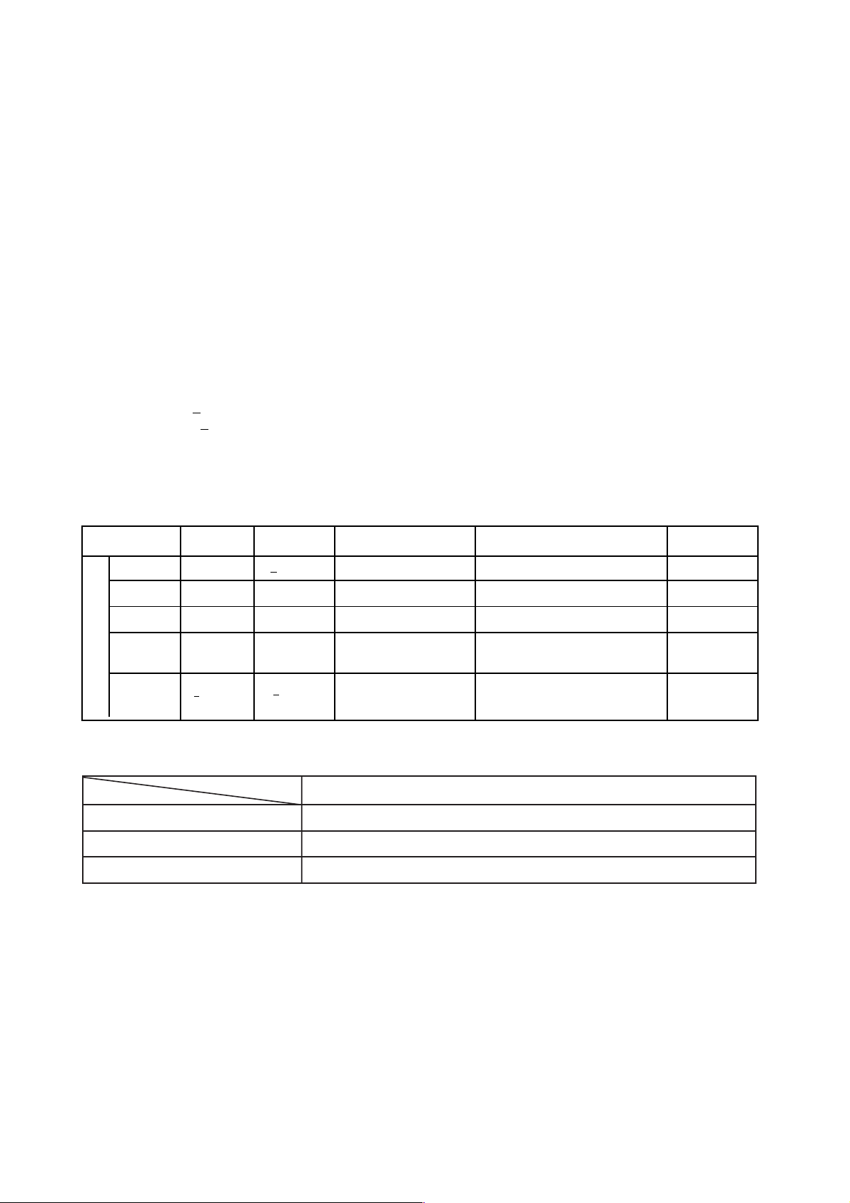
LOCATION OF CUSTOMER CONTROLS
6
1. Disc tray
This is the tray for the disc. Place the disc on the
ejected disc tray, then lightly push the tray (or
push the eject button) and the CD will be loaded.
NOTE: Don’t pull out or push in the disc tray
forcibly. This might cause damage to the loading
section of the drive.
2. Stop/Eject button
This button is pressed to open the CD tray.
This button works only when power is supplied to
the drive.
If an Audio CD is playing, pressing this button will
stop it, and pressing it again will open the tray.
3. Emergency Eject Hole
Insert a paper clip here to eject the Disc tray
manually or when there is no power.
4. Volume control
This is used to adjust the output volume of the
headphone jack. It can’t be used to adjust the
output volume for the audio output connectors on
the rear panel.
NOTE : Turn the volume down before turning on
the power. Sudden loud noises can damage your
hearing.
5. Headphone jack
This jack is for connecting headphones or minispeakers.
6. Drive activity indicators
Two colored LEDs are used to indicate the
operation of CD-R/RW Drive.
(1) Read
The orange color is displayed when the spindle
motor begins the Spin up operation: accessing
data, reading data, playing Audio, and up loading
tray.
(2) Write
The green color is flashed during disc writing
sessions.
READ
READ
WRITE
WRITE
Headphone Jack
Volume
Control
Drive Activity Indicators
Stop/Eject Button
Disc Tray
Emergency Eject Hole
Front Panel
Page 5
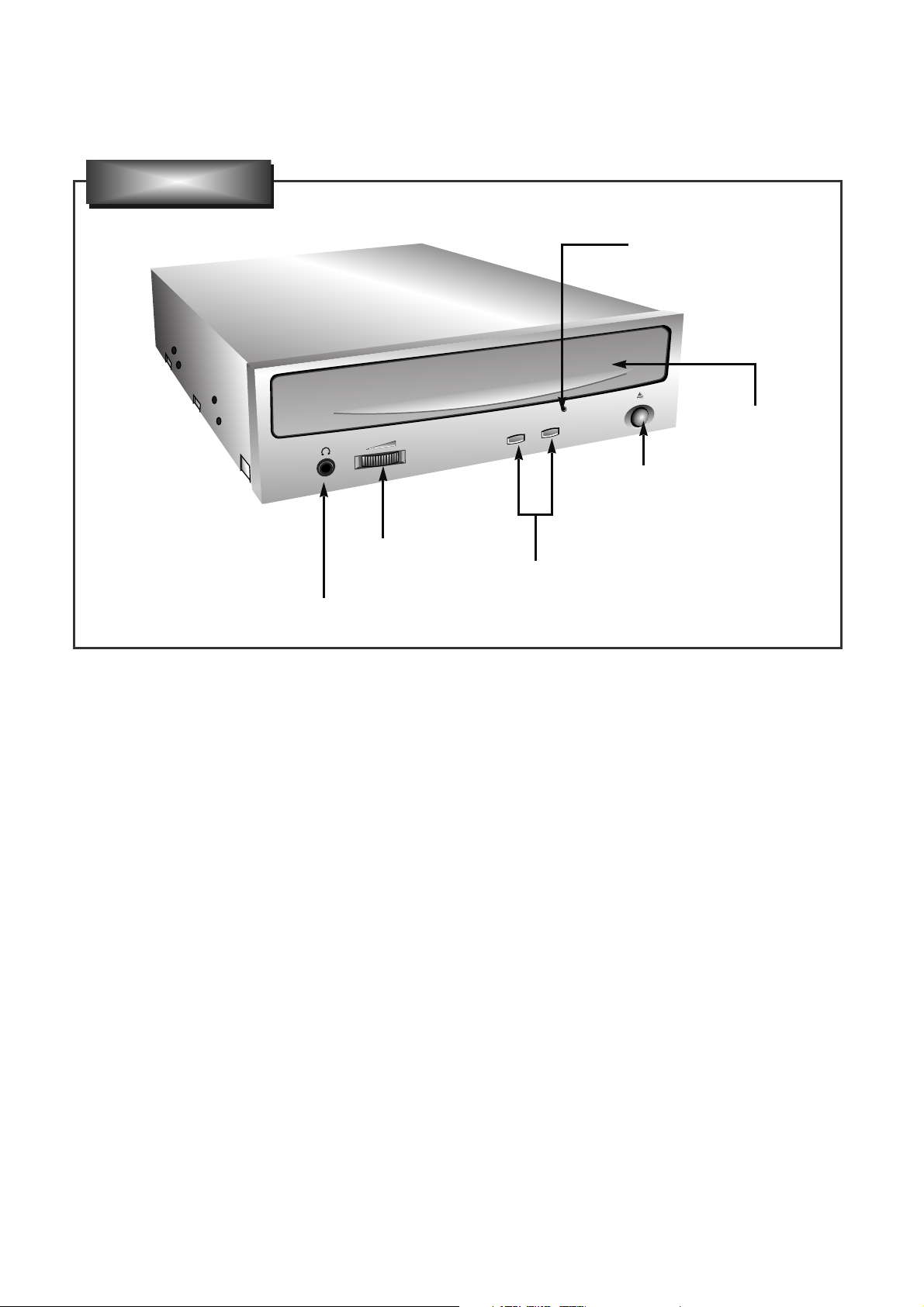
7
1. Power Connector
Connects to the power supply (5-and 12-V DC) of
the host computer.
NOTE : Be careful to connect with the proper
polarity. Connecting the wrong way may damage
the system (and is not guaranteed). Usually this
connector can only be attached one-way.
2. IDE Interface Connector
Connect to the IDE (Integrated Device
Electronics) Interface using a 40-pin flat IDE
cable.
NOTE : Do not connect or disconnect the cable
when the power is on, as this could cause a short
circuit and damage the system. Always turn the
power OFF when connecting or disconnecting the
cable.
3. Jumper Connector
This jumper determines whether the drive is
configured as a master or slave. Changing the
master-slave configuration takes effect after
power-on reset.
4. Analog Audio Output Connector
Provides output to a sound card (analog signal).
Generally you need this to play a regular audio
CD.
5. Digital Audio Output Connector
Provides output to a sound card (digital signal).
Digital Audio Output
Connector
Jumper Connector
Analog Audio Output Connector
IDE Interface Connector
Power Connector
Rear Panel
Page 6
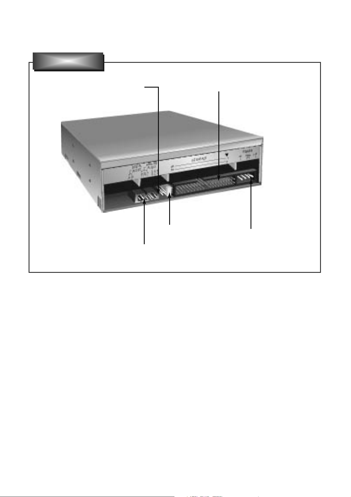
1. CABINET and CIRCUIT BOARD
DISASSEMBLY
1-1. Bottom Chassis
A. Release 4 screws (A) and remove the Bottom Chassis
in the direction of arrow (1). (See Fig.1-1)
1-2. Front Bezel Assy
A. Insert and press a rod in the Emergency Eject
Hole and then the CD Tray will open in the direction
of arrow (2).
B. Remove the Tray Door in the direction of arrow
(3) by pushing the stoppers forward.
C. Release 3 stoppers and remove the Front Bezel Assy.
1-3. Cabinet and Main Circuit Board
A. Remove the Cabinet in the direction of arrow (4).
(See Fig. 1-3)
B. Release 2 hooks (a) and remove the CD Tray
drawing forward.
C. Remove the Main Circuit Board in the direction of
arrow (5).
D. At this time, be careful not to damage the 4
connectors, are positioned at right side, of the Main
Circuit Board.
2. MECHANISM ASSY DISASSEMBLY
2-1. Pick-up Unit
A. Release screws (B).
B. Separate the Pick-up Unit in the direction of arrow (6).
(4)
(5)
Main
Circuit Board
Hooks (a)
Cabinet
(A)
(A)
(A)
(A)
(1)
Bottom Chassis
Fig. 1-1
Fig. 1-2
DISASSEMBLY
8
Fig. 1-3
Mechanism Assy
Pick-up Unit
(B)
(B)
(6)
Fig. 2-1
(3)
Stoppers
Emergency Eject Hole
(2)
Tray Door
Front Bezel Assy
CD Tray
Page 7
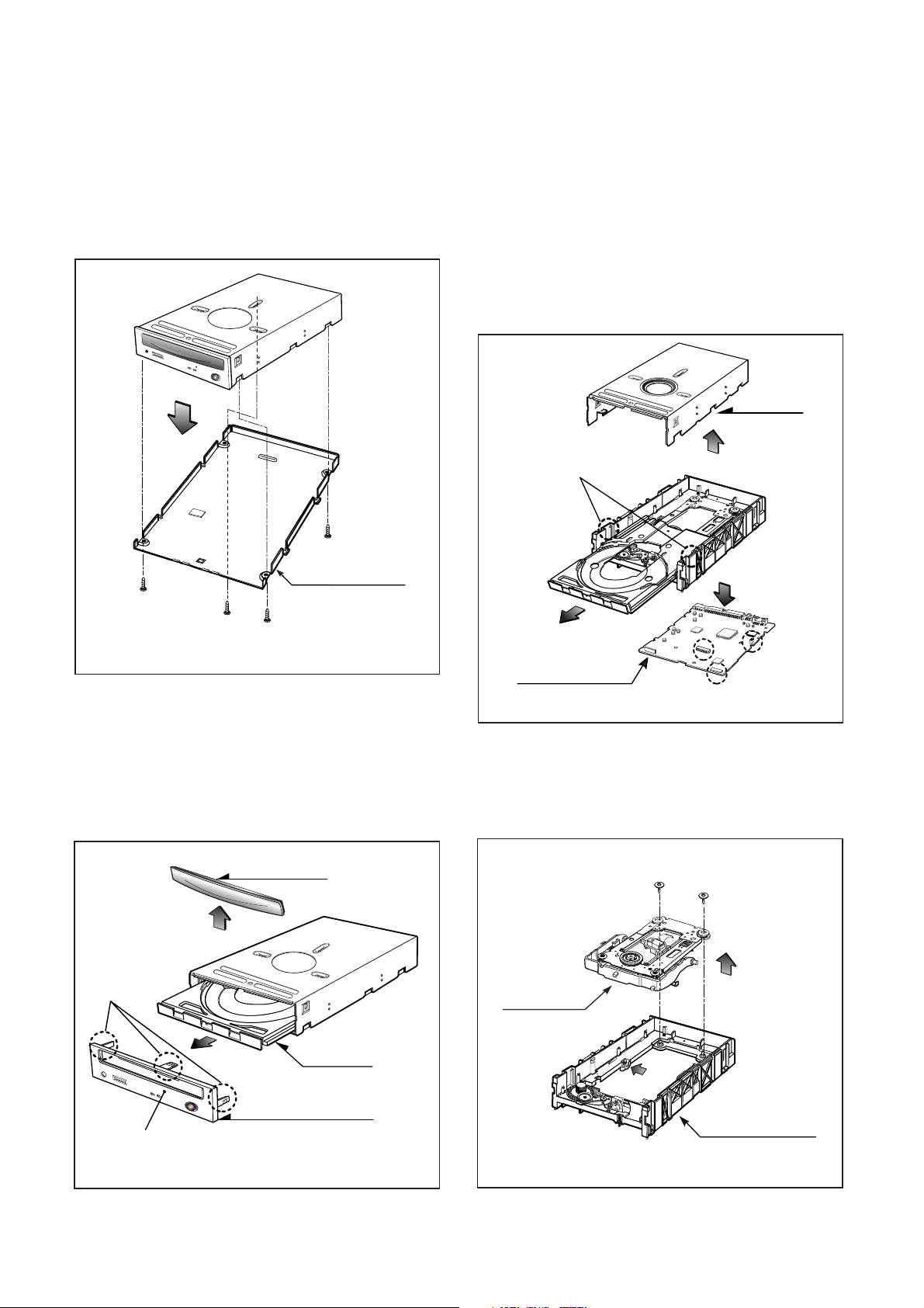
2-2. Pick-up
A. Release 2 screws (C) and remove the Pick-up.
Pick-up Unit
Pick-up
(C)
(C)
Fig. 2-2
9
Page 8
ATIP Absolute Time in Pre-groove. With an additional modulation of the “Wobble”, the “Groove” contains a time
code information.
Wobble The pre-groove in the Disc is not a perfect spiral but is wobbled.
With : – A typical amplitude of 30 nm
– A spatial peried of 54~64 µm
CW Continuous Wave. The laser light output is at a constant level.
DOW Direct Over-Write. The action in which new information is recored over previously recorded information in
CD-RW disc.
Overwrite
The action in which new information is recorded over previously recorded information.
(Pre-)Groove
The guidance track in which clocking and time code information is stored by means of an FM
modulated wobble.
Land Land is characterized in the following way:
When radial signals are concerned,land is defined as the area between the grooves.
When HF signal are concerned,land is defined as the area between the marks(pits) in tangential
direction.
Hybrid Disc A Multisession disc of which the first Session is mastered. On a hybrid disc, recorded and
mastered information may co-exist.
Mastered Information,stored as pits on the disc during the manufacturing process of the disc.
Information (when making the master)
OPC Optimum Power Control. Procedure is determined optimum recording power according to CD-
R/RW Media in recording start step.
ROPC Running OPC. The purpose is to continuously adjust the writing power to the optimum power
that is required.
When the optimum power may change because of changed conditions of disc and change in
operating temperature.
Jitter The 16 value of the time variation between leading and trailing edges of a specific (I3 … I11) pit
or land as measured by Time Interval Analysis.
Deviation The difference between a fixed value of Pit length and Land length.
TOC Table Of Contents : in the Lead-in Area the subcode Q-channel contains information about the
Tracks on the disc.
Packet A method of writing data on a CD in small increments.
Writing Two kinds of packets can be written : Fixed-length and Variable-length.
Write The shape of the HF write signal used to modulate the power of the laser.
Strategy The Write Strategy must be used for recordings necessary for disc measurements.
Information Wobble, ATIP, Disc Identification, Write Power, Speed Range OPC Parameters, etc are
Area recorded in the Information area of CD-RW Disc
Finalization The action in which (partially) unrecorded or logically erased tracks are finished and the Lead-in
and/or Lead-out areas are recorded or overwritten with the appropriate TOC subcode.
Logical Erase
A method to remove information from a disc area by overwriting it with an EFM signal containing
mode 0 subcode
A logically erased area is equivalent to an unrecorded
Physical Erase
The action in which previously recorded information is erased by overwriting with a CW laser
output.
After a Physical Erase action, the erased area on the CD-RW disc is in the unrecorded state
again.
Session
An area on the disc consisting of a Lead-in area, a Program area, a lead-out area.
Multi session
A session that contains or can contain more than one session composed Lead-in and Lead-out
GLOSSARY
14
Page 9
The differences of CD-R/CD-RW discs and General CD-ROM
1. Recording Layer
Recordable CD has a wobbled pre-groove on the surface of disc for laser beam to follow track.
2. Disc Specification
Read-only Disc
CD-R and CD-RW Disc
3~11T
1.6um
0.4~0.5 um
(Pit)Groove
Land
Track pitch(p)
Radial Direction
Iw
A
O
a
a
Groove
Land
Radial Error Signal
The Groove wobble
Average center
Actual center
CD-ROM CD-R CD-RW
Standard Yellow Book Orange Book II Orange Book III
Record Not available Write once Re-writable
I 11/Itop
> 0.6 > 0.6 0.55 > M11> 0.70
(HF Modulation)
Write Laser Power(mW) 10-30 mW 6-25 mW
Read Laser Power(mW) < 0.5 mW < 0.7 mW < 1.0 mW
Jitter < 35 nsec < 35 nsec < 35 nsec
Reflectivity (R
top) 70 % 65 % 15 % ~ 25 %
15
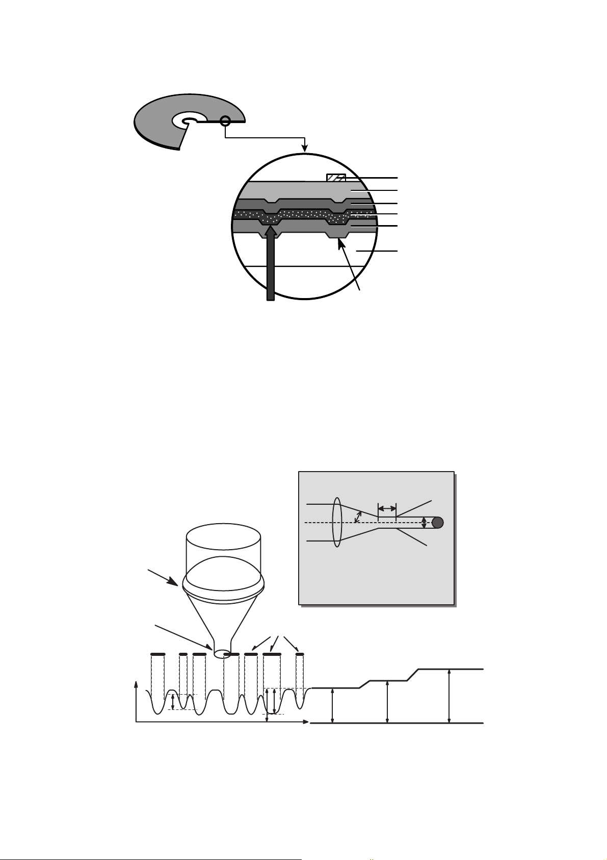
CD-ROM (READ-ONLY DISC)
a=30nm
Page 10
16
3. Disc Materials
1) CD-ROM disc
Laser Beam
Groove
Substrate
(Polycarbonate)
Organic Dye Layer
Reflective Layer
Protective Layer
Label Printing
2) CD-R disc
Pigment Reflective Layer Color
Phtalocyanine Gold/Silver Yellow/White
Cyanine Gold/Silver Dark Green/Bright Green
Azo Gold/Silver Dark Blue
• It is composed of Silver _ colored aluminum plate and Reflective layer.
• Groove (Pit) of aluminum plate make a track.
• Laser wavelength : 780 nm, Laser Power (Read): 0.5mW
• Signal is detected by the
difference of reflective beam
intensity between “pit” and
“Land” on the disc.
• It is so-called WORM (Write Once Read Many) CD.
• It is composed of polycarbonate layer, Organic dye layer, Reflective layer, and Protective
layer.Gold/Silver Reflective layer is used to enhance the reflectivity
• According to the kinds of Organic dye layer, it is divided by Green CD, Gold CD, Blue CD.
• Laser Wavelength : 780 nm, Laser Power (read) : 1.2 mW
• Recording Power : 8x(9~30mW), 12x(12~38mW), 16x(14~44mW), 24x(18~50mW)
• When some part of dye layer is exposed to laser heat, it’s color changs black.Therefore, writing and
reading is enabled by the difference of reflectivity between changed part and unchanged part.
• Polycarbonate layer has Pre_Groove which make a Track.
Laser Beam
Pit
Substrate
(Polycarbonate)
Reflective Layer
Protective Layer
Label Printing
Page 11
17
3) CD-RW Disc
4.
Reading process of Optical Disc
Laser Beam
Groove
Substrate
(Polycarbonate)
Reflective Layer
Dielectric Layer(TL)
Dielectric Layer(UL)
Protective Layer
Label Printing
• It is composed of polycarbonate layer, alloy(silver, arsenic) layer, aluminum reflectivity layer, protective layer.
• An crystalized alloy layer is transformed into noncrystalized by the laser heat. Therefore, writing and reading
is enabled by the difference of reflectivity.
• It is possible to overwrite about 1000 times.
• Laser Wavelength : 780 nm, Laser Power (Read) : 1.0mW
• Recording Power : Erase (4~18mW), Write (15~40mW)
• When disc rewriting, new data is overwritten previously recorded data.
• Polycarbonate layer has a Pre-Groove which make a track.
Lens
H
D
Beam
Spot
Focusing
Lens
Laser Spot
at Constant
Read Intensity
Reflected
Light
Signal
Laser Spot
Position
(Time)
Previously Recorded Marks
Groove Land Mirror
I
3
I
top
I
11
I
G
I
L
I
0
Numerical aperture: NA=nsinθ,
n: Refractive index
Focus depth : H =
λ
/NA
laser spot diameter : D =
λ
/NA
2
θ
Page 12
18
5. Writing Process of CD-R Disc
a b c d e f g
a
b
c
d
e
f
g
Incident
Laser
Powe r
(Read)
(Read)
(Write)
Laser Spot
Position
(Time)
a b c d e f g
Laser Spot
Position
(Time)
Laser
Spot
Recorded
Mark
Reflected
Light
Signal
Reflected
Light
Signal
Below "ORP"– Mark Too Short
At Optimum Record Power ("ORP")
Above "ORP" – Mark Too Long
Time
6. Writing process of CD-RW Disc
Write Power
Erase Power
Read Power
Groove
Crystal
Amorphous
Amorphous
Recorded state
(lower reflectivity)
Melting/
quenching
Heating/
gradual cooling
Crystal phase
Erased state
(higher reflectivity)
Page 13
7. Organization of the PCA, PMA and Lead-in Area
1) Layout of CD-ROM disc
19
Center hole Clamping and Label Area Information Area
Lead-in Area
Lead-in Area
Diameter 15 mm
Diameter 46 mm
Diameter 120 mm
Program Area
Read Only Disc
Lead-out Area
Program Area Lead-out Area
Center hole
Clamping and Label Area
Information Area
PCA PMA
Test Area Count Area
Diameter 15 mm
Diameter 45 mm
Diameter 120 mm
Unrecorded Disc
Tsl-00:35:65 Tsl-00:15:05
Tsl-00:13:25
Tsl
99:59:74
00:00:00
in out
Test Area : for performing OPC procedures.
Count Area : to find the usable area immediately in T.A
Tsl : start time of the Lead-in Area, as encoded in ATIP
PMA : Program Memory Area
Disc Center
Disc Center
2) Layout of CD-R/RW disc
Page 14
20
8. Function of PCA and PMA area
1) PCA (Power Calibration Area)
• PCA area is used to determine the correct Laser Power for a disc.
– Method 1 : PCA area is divided by a track.
– Method 2 : The previous Calibration value is referred.
– Method 3 : ROPC is used to determine Laser Power value automatically in data writing.
• CD-R Disc can write maximum 99 Tracks but CD-RW Disc can write unlimited tracks because it has a rewritable
function.
2) PMA (Program Memory Area)
• It has a track information (track No, track Start/End time) of every track before writing completed.
– PMA area has the last written point and the next writable point of a disc.
– In case of CD to CD copy, some writer may not write PMA area.
* When Disc is Finalized,
PMA information is transferred to the Lead_In area so that general Driver can read it.
* Because PCA and PMA area exist before Lead-In area, General CD Player or CD-ROM Drive can’t read
these areas.
9. OPC and ROPC
1) OPC (Optimum Power Control)
• This is the first step of writing process, because CD writer has its own laser power value and media have different
writing characteristics,
– This is determined by the Writing characteristic, speed, temperature, and humidity.
– Laser wavelength is determined by the environmental temperature (775~795nm) and Optical Laser Power is
determined by the test and retry.
• Asymmetry and optimum writing Power
– EFM signal Asymmetry is determined by the writing power.
Therefore, Optical Power which has the same value to the preset power value can be estimated by measuring
HF signal Asymmetry on the PCA area.
• Measurement of Asymmetry
* Parameter setting (Beta) : Using AC coupled HF signal before equalization
Beta = (A1+A2)/(A1-A2)
Time
P << Po
Time
P = Po
HF Signal
A1
0
A2
Time
P >> Po
Page 15
2) ROPC (Running Optimum Power Control)
• Variable primary factor of Optimum Power
– Change of Power sensitivity on the Disc. (limited to 0.05 *Po)
– Wavelength shift of the laser diode due to the operating temperature change.
– Change of the Spot aberration due to the Disc skew,
Substrate thickness, Defocus.
– Change of Disc or Optics conditions due to the long term OPC
==> It is necessary to adjust continuously to obtain the Optimum Power.
• Principle of Running OPC
– To meet the factors mentioned above,
a horizontal _ direction movement of a curve is uesd.
– Beta = f(B-level) = constant on the Recorded Disc
– Procedure of ROPC
a. Reference B-level is determined during OPC Procedure.
b. During Recording, B-level value is controlled to have a close
Reference B-level value.
c. Normalization of B-level is used to eliminate the effect of reflectivity fluctuation.
==> The reflected B-level value is normalized by the disc reflectivity itself.
21
CD-R/RW Media
Write Strategy
Determination
PCA Test Area
Program Area
PMA Area
Lead-In Area
Lead-out Area
OPC
PCA Count Area
ROPC
* Recording Capacity of CD-R/RW (74Minute Recording media)
• (2048 Byte/Sector) X (75 Sector/Second) X (60 Second/Minute) X 74 Minute
= 681,984,000 Bytes = 682 Mbytes
• But the actual recording capacity is about 650 Mbytes. (according to the ISO 9660 standard, approximately
30 Mbytes are used to make directory structure and volume names.)
Incident recording pulse
Reflected recording pulse
Sampled timing B
11T
Sample B-level (Write Power)
Level B
Sampled at timing B
Pwo decided by OPC
Recording Power
Level B with Pwo
normalized to recording power
Sample Disc Reflectivity
(Read power)
10. Writing Process of DISC
Page 16
INTERNAL STRUCTURE OF THE PICK-UP
1. KRS-310B Circuit Diagram
22
1
2
3
4
5
6
7
1
2
3
4
5
1
2
3
4
5
6
7
8
9
10
11
12
13
14
15
16
17
18
19
20
21
22
23
24
14
13
12
11
10
9
8
10
9
8
7
6
R3
VR1
VR2
R2
C5
C3
C6
LD
A
11
C
C4
R4
R1
L1
R6
R7
C7
R8
C10 C9 C8
Vcc
2 Axis Actuator
IC1
PDIC
IC2 FPDIC
C1
R9
R11
R12
R10
C2
GND
G
D
C
E
RF
SW
GND
H
A
B
F
Vc
NC
GND
GNDGND
VccVc
BinOUT
PDIN
VOUT
VCC
VREF
VCC
GND
IOUT
IINR
IOUT
IIN2
GND
IIN3
GND
RFREQ
RAMP
GND
ENABLE
GND
OSCEN
WEN3
VCC
WEN2
GND
GND
7
8
9
10
11
12
13
14
15
16
17
18
19
20
21
22
23
24
25
26
27
28
29
30
31
32
6
5
4
3
2
1
FCS +
FCS -
TRK +
TRK -
G
D
C
E
RF SUM
SW
PDGND
PDVC
F
B
A
H
PDVCC
FPDO
FPDVCC
FPDGND
FPDVC
LDVCC
LDVCC
VRDC
VWDC1
VWDC2
LDGND
LDGND
WE1
WE2
OSCEN
33
34
ENBL
MODAMP
IC3
LD
Driver
Page 17
2. Signal detection of the P/U
1) Focus Error Signal ==> (A+C)-(B+D)
This signal is generated in RF IC (IC401 : CXA2638R) and controls the pick-up’s up and down to focus on
Disc.
2) Tracking Error Signal (DPP Method) ==> {(A+D)-(B+C)}- kx {(F+H)-(E+G)}
This signal is generated in RF IC (IC401 : CXA2638R) and controls the pick-up’s left and right shift to find
to track on Disc.
3) RF Signal ==> (A+B+C+D)
This signal is converted to DATA signal in DSP IC (IC201 : OTI-9797).
23
Pick-Up module
Photo Diode
Tracking
Focusing
Infrared Iaser
k[(F+H) - (E+G)]
(A+D) - (B+C)
(A+D) - (B+C) - k[(F+H) - (E+G)]
Offset
TE
Tp
Sub2
Main
Tp/2
Sub1
Track Center
F, E
D,C
A,B
H,G
Page 18
DESCRIPTION OF CIRCUIT
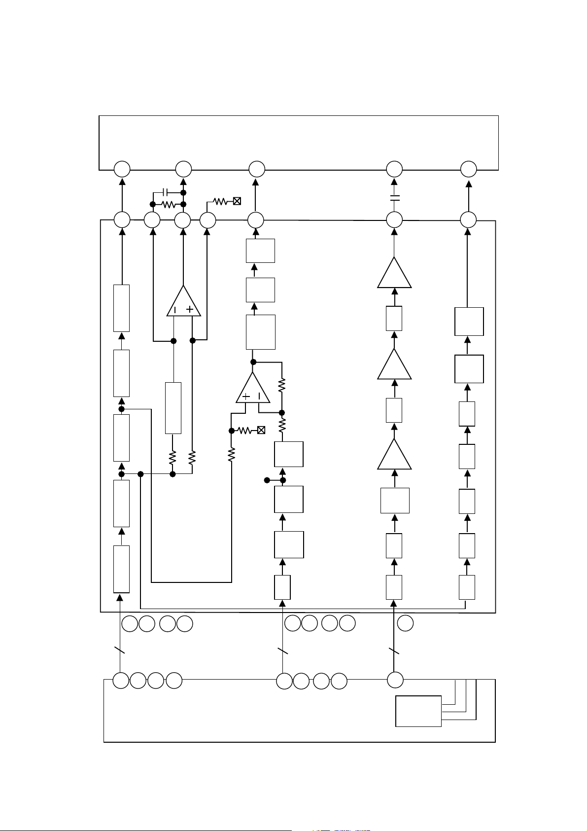
1. ALPC (Automatic Laser Power Control) Circuit
1-1. ALPC Loop Circuit
24
RFPDG
FPDO
AUX
FVREF
WFPDSH
HOLDSW
WLDON
WR/RE
WGATE
WR/RE
WGATE
EFM1
EFM2
R321
C4
R322
R427
R426
C454
C443
R447
D401
GND
R19
VWDC
WREF
HOLDTC
ODREF
APCCSW
R18
R408
C432
VWDCN
APCCSW
WREFSE
S3.
B
B
R14
25.8K
R15
25.8K
GND
GND
A
A
R12
R10
5K
R6
20K
R3
R4
20K
20K
R8
20K
10K
GND
GND
C3
SCLK
DACS
WREFSE
C445
R252
R247
R429
SHOUT
RFPDSH
20dB/26dB
3.3V
R422
R423
IC403
IC205
IC301 MICOM
IC201
OTI-9797
C456
C455
MPXOUT
(testmode)
MPXOUT
(testmode)
VRDCN
VRDC
VRDC
R16
R17
R410
C433
R11
10K
GND
GND
RREFSE
R9
5K
R1
20K
R2
20K
A:OFF
B:ON
A:OFF
L:B.HOLD
H:A.SAMPLE
B:ON
RREF
WREF
ODREF
SHOUT
WRITEG WFPDG
DAC
DAC
DAC
GNDTyp.
10mV/step
sbit
GND
GND
Typ.
10mV/step
8 bit
Typ.
10mV/step
7 bit
H:RREF
R13
R5
R7
20K
(Read)
(Write)
20K
25.8K
GND
L:OPEN
H:OPEN
L:WREF
RLDON
ERCNT
8
GND
C1
96
94
97
98
25
19
22
100
32
99
62
1
31
45
48
3
5
6
7
166
188
180
183
184
60
6564
24
92
90
91
17
16
15
5
4
18
13
95
PN401
P/U
TC7W08FV
IC401 CXA2638R
FPDVC
FPDO
VRDC
26
VWDC
27
VWDC2
30
WE1
31
WE2
x1
S/H
S/H
Gain
adj.
IC402
DAC
x1
S/H
Page 19

1-2. ALPC(Automatic Laser Power Control) Circuit Operation
This circuit consists of Feedback Loop to maintain light output of the Laser Diode(FPDO).
Feedback signal, output voltage from PD(Photo Detector) of P/U, is used monitor the light power of
Laser Diode.
1) Read Loop
RREF(Read Reference Voltage) of IC401(CXA2638R) Pin 96, which is from DAC(IC403) Pin 18, is the
reference level of the Read Loop part of this ALPC Circuit.
• When Playback
VRDC(Pin 97) signal of IC401(CXA2638R) is output to P/U through Gain Control S/W and drives
Laser Diode during play back.
This S/W Ciruit is designed to reduce transition time from CD-RW writing mode to playback mode.
• When writing mode
- CD-R
Three Laser Power Levels, Read, Write, and Overwrite, are used to write on CD-R disc, and Read
Level is used to monitor the output laser power.
For stabilizing read loop, the S/H signal(RFPDSH), which sample and hold the Read Level of laser
power in the CD-R writing mode, is input through Pin 32 of IC401(CXA2638R).
- CD-RW
Three Laser Power Levels, Read, Erase and Write, are used to write on CD-RW disc, and Erase
Level is used, during CD-RW writing, to monitor output laser power.
It is not VRDC but VWDC that is the output signal of the control loop performed by Erase level.
2) Write Loop
For stabilizing write Loop, the S/H signal(WFPDSH), which sample and hold the Erase Level of laser
power in the CD-RW writing mode, is input through Pin 31 of IC401(CXA2638R).
Output voltage of Write Loop, VWDC(Pin 93 of IC401(CXA2638R)), is protected by the high limit diode
applied to P/U.
25
Page 20
2. RF Amplifier Circuit
Block Diagram
26
FE
FE
A,B,C,D
E,F,G,H
RFSUM
PDIC
VC
GND
Vcc
CXA2638R (IC401)
IC201
OTI9797
Pick up
KRS-310B
Gain Amp
16
15
8
7
9
14
6
17
10
7
59 197
8
9
10
87
2
3
4
5
Offset adj
R1
R2
R3
R4
R6R5
R403
C417
R404
Vref
Main S/H Gain adj Offset adj
CEM
CEO
CEP
TE
CE
198
204
TE
58
EQRFP
C223
EFM
163
ATFG
WOBBLE
132
Limit
Gain
Amp.
Side
S/H
SPPO
4((F+H)-(E+G))
MPP 2(A+D)-(B+C))
DVC
Gain
adj
Gain
adj
Offset
adj
LPF
(40KHz)
Gain
adj
offset
adj
Limit
GCA HPF
HPF AGC BPF AGC
Slice
circuit
HPF
EQ HPF
636567
x0.25 x5 x3.2
71
38
Page 21
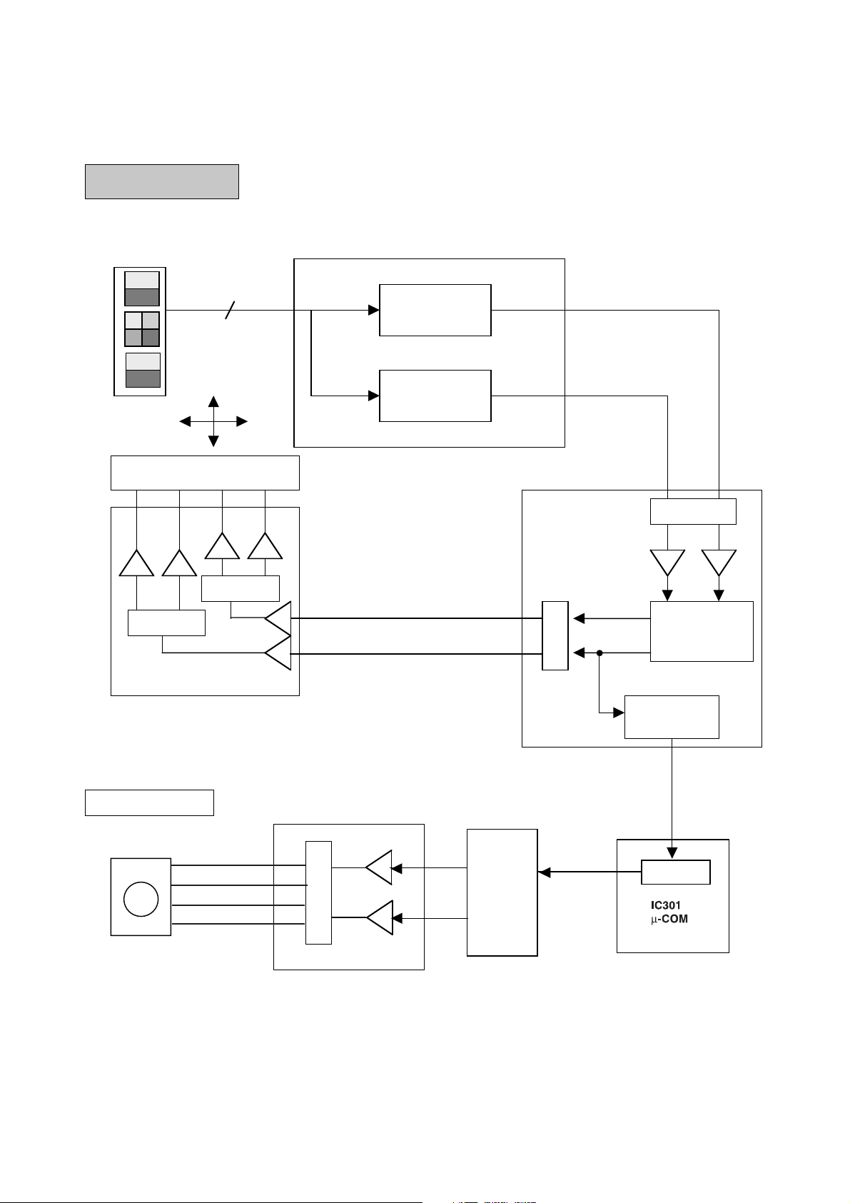
3. Focus/Tracking/Sled Servo Circuit
3-1. Focus, Tracking & Sled Servo Process
27
Focus, Tracking Servo
C
B
D
A
E
F
G
H
Pick- up
A,B,C,D,E,F,G,H
A,B,C,D
Focus Error
Detector
Detector
Track Error
A,B,C,D
E,F,G,H
IC401 CXA2638R
FE
TE
TE FE
A/D
Low freq Gain Filter
Ditital EQ
DAC
Sled Control
Signal
A/D
IC201
Servo Control
OTI9797
LEVEL SHIFT
LEVEL SHIFT
Tracking Focusing
Actuator
FAO
TAO
SLO
F+
F-
T+
T-
Sled Control
M
SLED MOTOR
LEVEL SHIFT
SM_A-
IC501
BD7902C
SM_A+
SM_B+
SM_B-
IC501 BD7902C
IC402
BU2500FV
(DAC)
Page 22

3-2. Focus Servo
The aim of Focus Servo is to maintain the distance between object lens of P/U and disc surface, so that
the detected RF signals (A, B, C, D) can be maximized.
Focus Servo is based on focus error (FE) signal which is generated from focus error detection block in
CXA2638R(IC401) using Astigmatism Method. Focus gain and path can be changed at the CXA2638R
according to the disc, and the resulting output (FE) is input to Servo IC (IC201, OTI9797).
FE signal after first amplification in OTI9797 is A/D converted and input to Digital Equalizer Block, most
important part at the Focus Servo. At the Digital Equalizer, adjustments for Focus Bias and Loop Gain are
performed.
After D/A converted, Focus servo signal is output through FOO port (OTI9797, Pin207) and drive Focus
Actuator through the Focus Drive IC (IC501, BD7902C).
3-3. Tracking Servo
The aim of Tracking Servo is to make laser beam trace the data track on disc. Tracking Error (TE) signal
is generated from tracking error detection block in CXA2638R (IC401) using DPP (Differential Push-Pull)
Method. DPP method uses not only main beam (A, B, C, D) but side beams (E,F and G, H) for correcting
DC offset generated in Push-Pull method.
The remaining procedures of TE signal processing in CXA2638R is similar to Focus Servo.
After D/A converted, Tracking servo signal is output through TRO port (OTI9797, Pin208) and drive
Tracking Actuator through the Tracking Drive IC (IC501, BD7902C).
3-4. Sled Servo
The working distance of tracking actuator is too short to cover whole disc radius. Sled Servo make PU
move by little and little so that the laser beam keep tracing the data track on disc continuously when
tracking actuator reaches the working limit.
Another function of Sled Servo is to seek a target point on disc, following user commands.
Sled control signal, STEP-CTRL0,1 from BU2500FV is generated in µ-com, STEP-CTRL0,1 are output to
sled motor via IC501(BD7902C).
28
Page 23

4. Spindle Servo Circuit
4-1. Spindle Servo Process
4-2. Spindle Servo
Spindle servo is as followings;
1) Wobble CLV x2, x4, x8, x10, x12, x16, 24x : Blank area in CD-R, CD-RW.
2) CD 8x-20x CAV: Eccentric CD-R/RW.
3) CD 14x-30x CAV: Video CD, CD-DA in CD-ROM/R
4) CD 32x CAV: Recorded area in CD-RW.
5) CD 40x CAV: CD-ROM. Recorded area in CD-R.
– Spindle Servo is controlled by IC401 (CXA2638R), IC201(OTI9797) and servo signal is output via
DMO ( pin2, OTI-9797).
29
Pick- up
IC401 CXA2638R
Wobble Signal
Generator
RF
SRF
EQRFP
ATFG
Decode PLL
Frequency
Controller
CD-DSP/SERVO
LOCK
DEFS
MOTOR SPEED
CONTROLLER
FILTER
TON
DMO
ATIP CLV, FG
Level Shif t
Hall Sensor
M
Spindle Motor
IC 301
u-COM
MUTE
SPNFG
IC201 OTI9797
CD EFM CL V
CAV x32
6
8
E
CB
DA
F
G
H
IC501 BD7902C
Page 24

MAJOR IC INTERNAL BLOCK DIAGRAM AND PIN DESCRIPTION
IC401 (CXA2638R) : CD-R/RW Analog Signal Processor
Block Diagram
30
RFEQ
PH/BH
CE
RFRP
REGISTER
ATIP
S/H MATRIX
BIAS
APC
VC
MPX
SPP
SADBC
EFGH
FEO
SPPO
ADO
BCO
RFO
SADO
SBCO
FE TE
BETA
RECD
96
RREF
97
VRDC
98
VRDCN
99
SHOUT
100
FPDO
95
APCCSW
94
VWDCN
93
VWDC
92
WREF
91
ODREF
90
HOLDTC
89
VTIREF
88
GND
87
RFIN
86
Vcc
85
RRF
84
RRFIN
83
BHC2
82
PHC2
81
BHO2
80
PHO2
79
BETAOUT
78
BHC3
77
BHC1
76
75
PHC1
BHO174PHO173RECD1C72EQRFN71EQRFP70SRFO69RFRP68RFCT67CEP66GND65CEM64Vcc63CEO62AUX61MPXOUT60MPP59FE58TE57TEIN56TOK1C55TOK2C54RFCTC153RFCTC252XTOK
51
50
XTOR
XTAND
49
CS
48
WLDON
47
TFGCNT
46
AGCON
45
HOLDSW
44
ERGCNT
43
SCLK
42
SDATA
41
XLAT
40
Vcc
39
DVcc
38
ATFG
37
RECD
36
GND
35
ROPCSH
34
M/SPDSH
33
WBLSH
32
RFPDSH
31
WFPDSH
30
DSPVcc
29
VC
28
DVC
27
HDVC
26
25
VCT1
VCT2
24
CAVC3
23
CAVC2
22
CAVC1
21
CAV_CNT
20
ATFM
19
AGC3C
18
AGC3C
17
AGC1C
16
BGIREF
15
SBADO
14
Vcc
13
WRF
12
GND
11
SWRF
10
HIN
9
GIN
8
FIN
7
EIN
6
HAVC
5
DIN
4
CIN
3
BIN
2
AIN
1
FVREF
Page 25

31
• Pin Assignment
Pin no Symbol I/O Description
1 FVREF I Reference voltage of APC input signal
2 AIN I Input of Main beam signal(A)
3 BIN I Input of Main beam signal(B)
4 CIN I Input of Main beam signal(C)
5 DIN I Input of Main beam signal(D)
6 HAVC I Reference Voltage of Main and Side beams
7 EIN I Input of Side beam signal (E)
8 FIN I Input of Side beam signal (F)
9 GIN I Input of Side beam signal (G)
10 HIN I Input of Side beam signal (H)
11 SWRF O Output of Write RF sample signal
12, 36, 66, 88 GND * Ground
13 WRF O Output of Write RF signal
14, 40, 64, 86 VCC * Analog Power
15 SBADO O Output of SRFO and EFGH Balance signal
16 BGIREF * Reference Voltage of Resister
17 AGC1C * External Capacitor connection for AGC1 Detection Time Constant
18 AGC2C * External Capacitor connection for AGC2 Detection Time Constant
19 AGC3C * External Capacitor connection for AGC3 Detection Time Constant
20 ATFM O Output of Wobble signal
21 CAV_CNT I Input of BPF control voltage for CAV mode
22 CAVC1 * External Capacitor connection for Peak Hold Detection Time Constant
23 CAVC2 * External Capacitor connection for Peak Hold Detection Time Constant
24 CAVC3 * External Capacitor connection for BPF control voltage smoothing
25 VCT2 * Decoupling of VC
26 VCT1 * Decoupling of DVC
27 HDVC O Output of DVC/2 Voltage
28 DVC O Output of DSPVCC/2 Voltage
29 VC O Output of VCC/2 Voltage
30 DSPVCC * DSP Power
31 WFPDSH I Sample Pulse for Write APC Mode (H: Sample, L: Hold)
32 RFPDSH I Sample Pulse for Read APC Mode (H: Sample, L: Hold)
33 WBLSH I Sample Pulse for Wobble signal (H: Sample, L: Hold)
34 M/SPDSH I Sample Pulse for Main and Side Beams signal (H: Sample, L: Hold)
35 ROPCSH I Sample Pulse for Running OPC (H: Sample, L: Hold)
41 XLAT I Latch input
42 SDATA I Serial Data input
43 SCLK I Clock input for Serial Data transmission
45 HOLDSW I VWDC Hold control (H : Sample, L: Hold)
46 AGCON I AGC ON/OFF control (H:AGC ON, L: AGC RESET)
47 TFGCNT I Gain transmission control for TE and FE signal (H: 0 dB, L: -4dB)
48 WLDON I Transmission control for Write (H: LD ON, L: LD OFF)
37 RECD O Output of Recorded Area Detection signal
38 ATFG O ATIPFG output
44 ERGCNT O Output of Erase gain transmission control
50 XTAND O Output of Out-of -Track Detection signal (AND)
51 XTOR O Output of Track Amplitude Detection signal (OR)
Page 26

32
Pin no Symbol I/O Description
52 XTOK O Output of Out-of -Track Amplitude Detection signal
39 DVCC * Digital power
49 CS I Chip power save control (H: power ON, L: Power OFF)
53 RFCTC2 * External Capacitor connection of Peak Hold Time Constant for RFRP signal
54 RFCTC1 * External Capacitor connection of Bottom Hold Time Constant for RFRP signal
55 TOK2C * External Capacitor connection for Retriggerable mono multi Time Constant
56 TOK1C * External Capacitor connection for Retriggerable mono multi Time Constant
57 TEIN I Input of Tracking error signal
58 TE O Output of Tracking error signal
59 FE O Output of Focus error signal
60 MPP O Output of Main Push- Pull signal
61 MPXOUT O Multiplexer Output for Signal monitoring
62 AUX I Auxiliary input for Signal monitoring
63 CEO O Output of Center error AMP
65 CEP * Input of Center error AMP
67 CEM * Reverse Input of Center error AMP
68 RFCT O Output of RFRP Slice level
69 RFRP O Output of Radial contrast signal
70 SRFO O Output of RF Sample signal
71 EQRFP O Output of RF Equalizer
72 EQRFN O Output of RF Equalizer
73 RECD1C * External Capacitor connection for Retriggerable mono multi Time Constant
74 PHO1 O Output of Pick Hold
75 BHO1 O Output of Bottom Hold
76 PHC1 * External Capacitor connection for Peck Hold Time Constant
77 BHC1 * External Capacitor connection for Bottom Hold Time Constant
78 BHC3 * External Capacitor connection for Bottom Hold Time Constant
79 BETAOUT O Output of Beta Value
80 PHO2 O Output of Pick Hold
81 BHO2 O Output of Bottom Hold
82 PHC2 * External Capacitor connection for Pick Hold Time Constant
83 BHC2 * External Capacitor connection for Bottom Hold Time Constant
84 RRFIN I External Capacitor connection for RRF(85 Pin)
85 RRF O Output of Read RF signal
87 RFIN I Input of Main beam composite signal
89 VTIREF * Reference Voltage of Resister
90 HOLDTC * External Capacitor connection for VWDC Hold
91 TDREF O Output of Reference Voltage for Overdrive power
92 WREF O Output of Write Power Reference Voltage level control
96 RREF O Output of Read Power Reference Voltage level control
93 VWDC O Output of APC for Write
94 VWDCN * Reverse Output of APC Amp for Write
98 VRDCN * Reverse Output of APC Amp for Read
95 APCCSW * External Capacitor connection of APC time constant for Write
97 VRDC O Output of APC for Read
99 SHOUT O Sample hold output for signal monitoring
100 FPDO I Input of Laser Power Monitor Voltage
Page 27

IC201(OTI-9797) : CD-R/RW Encoder/Decoder/Write Strategy Chip
Block Diagram
33
Page 28

34
2.4.2 CD-ENCODER INTERFACE
Pin Name Pin # Type Description
XIN 137
X
IN
Crystal In: System clock
XOUT 136
X
OUT
Crystal Out: System Clock
AT I P C K /
WBLCLK
138 O ATIP Clock Out
ENCLK 6 I Encoder Clock Input
CLKOUT /
ARST#
65 O
General Purpose Clock Output
Pin Name Pin # Type Description
PA N I C I N 168
I
S
Panic Input
WBLIN 132
I
S
Wobble In: Wobble input digital signal
HFSW 167 O High Frequency Modulation Switch
WGATE /
NRZWGATE
166 O
Write Gate /
EFM NRZ Write Gate
EFM1 183 O EFM1: EFM output
EFM2 184 O EFM2: EFM output
EFM3 185 O EFM3: EFM output
EFMNT1 /
EFMNT1
/
ELPBS1
169 O
EFMNT1: EFM pit pattern length indicator /
EFMN : Non-Delayed EFM Pit Pattern Length Indicator /
ELPBS1: External Low Pass Filter Band Switch
CLOCK
CD-ENCODER INTERFACE
Page 29

35
EFMNT2 /
EFMNT2’ /
ELPBS2
170 O
EFMNT2: EFM pit pattern length indicator /
EFMN
: Non-Delayed EFM Pit Pattern Length Indicator /
ELPBS2: External Low Pass Filter Band Switch
EFMNT3 /
EFMNT3’ /
ELPBS3
171 O
EFMNT3: EFM pit pattern length indicator /
EFMN : Non-Delayed EFM Pit Pattern Length Indicator /
ELPBS3: External Low Pass Filter Band Switch
EFMNT4 /
EFMNT4’ /
ELPBS4 /
RWSW
172 O
EFMNT4: EFM pit pattern length indicator /
EFMN
: Non-Delayed EFM Pit Pattern Length Indicator /
ELPBS4: External Low Pass Filter Band Switch /
RWSW: CD-RW Write Gate Switch
E11TP /
EFMSY
175 O EFM11T Pit Pattern: EFM11T pit pattern indicator
E11TS /
MONIT /
SVSY
176 O EFM11T Space Pattern: EFM11T space pattern indicator
EFCK 177 O EFM Bit Clock: EFM bit clock generated from internal clock in CD encoder
SMP3 /
SYEQ
180 O SMP3: Sample and Hold Signal 3
SMP1 /
MONIT
181 O SMP1: Sample and Hold Signal 1
SMP2 /
ASYEQ
182 O SMP2: Sample and Hold Signal 2
SMP4 /
TLDLD
186 O SMP4: Sample and Hold Signal 4
SMP5 /
TPDLD
187 O SMP5: Sample and Hold Signal 5
SMP6 /
OPC11T /
RWS WI
188 O
SMP6: Sample and Hold Signal 6 /
RWSWI : CD-RW Write Gate Switch Inverted
Pin Name Pin # Type Description
Page 30

36
2.4.4 CD-SERVO INTERFACE
Pin Name Pin # Type Description
REVDET 4
I
S
Reverse Detect Motor Drive: Indicates spindle motor is rotating in reverse
direction
FG 5
I
S
FG IN: HG (tachometer) pulse input
MON 7 O Motor Drive On: Enables spindle motor drive
SBRK 8 O
Short Brake: Stops spindle motor by applying a short pulse to the motor
winding
AT I P C K /
WBLCLK
138 O Wobble Clock
EEFS /
LSRPREP
179 O EFM Frame Sync
ESFS /
EFMNRZ
178 O Encoder Subcode Frame Sync
Pin Name Pin # Type Description
DMO 2
O
A
Spindle Motor Servo Output
SLO 3
O
A
Sled Servo Output
FOO 207
O
A
Focus Servo Output: Focus servo feedback signal.
TRO 208
O
A
Tracking Servo Output: Tracking servo feedback signal.
TEBC 194
O
A
Tracking Error Balance Control
FE 197
I
A
Focus Error
TE 198
I
A
Tracking Error
BS 201
I
A
Beam Strength
RPBC 202
O
A
Ripple Balance Control
RP 203
I
A
Ripple of RF
WOBBLE MOTOR INTERFACE
CD-SERVO INTERFACE
Page 31

37
2.4.5 CD-DSP INTERFACE
RX 191
I
S
RP Zero Crossing: Used for fine search.
TX 192
I
S
TE Zero Crossing: Track crossing signal input used in conjunction with RX
to
perform fine searches.
CE 204
I
A
Center Position Error
LDON /
NDIVOUT
141 O
Laser Diode On / CAV Write N Divider: MUXing of this pin is controlled by bit
ATIPN (18Fh.7). - Not used.
TC 193
I
S
Track Count Input: High-frequency track crossing signal input used to
perform
rough searches and to increment the internal track counter.
FLAGA 142 O
Servo Monitor Flag A: FLAGA is used to output one of four internal servo
signals. FLAGA can also be used as a general output port.
FLAGB 145 O
Servo Monitor Flag B: FLAGB is used to output one of four internal servo
signals. FLAGB can also be used as a general output port.
FLAGC 146 O
Servo Monitor Flag C: FLAGC is used to output one of four internal servo
signals. FLAGC can also be used as a general output port.
FLAGD 149 O
Servo Monitor Flag D: FLAGD is used to output one of three internal servo
signals. FLAGD can also be used as a general output port.
Pin Name Pin # Typ e Description
EFM 163
I
A
EFM Analog Data
ASY 162
O
A
Asymmetry DAC Output
EFMR1 159
I
A
EFM Analog Data Bias 1
EFMR2 160
I
A
EFM Analog Data Bias 2
EFMR3 161
I
A
EFM Analog Data Bias 3
MONIT /
PLCK
133 O
CD-DSP Monitor Output: MONIT is used to output several internal CD-DSP
signals.
Pin Name Pin # Type Description
CD-DSP INTERFACE
Page 32

38
Pin Name Pin # T ype Description
MIO0 /
L–
143 I/O
Multiple I/O 0: MIO0 is used to output several internal test signals.
DEFAULT
Serial Data: This signal is for 16-bit PCM serial audio data.
It can
be used to send audio data to an external or internal OTI-9797 DAC.
Audio
data is in 24-bit slot format for input and output.
Differential Audio Output
MIO1 /
L+
144 O
Multiple I/O 1: MIO1 is used to output several internal test signals.
DEFAULT
Audio Left/R ight Clock: Indicates the start of the 24-bit value
on
SDATA. High indicates the start of the left channel.
L+: Differential Audio Output
MIO2 /
R+
147 O
Multiple I/O 2: MIO2 is used to output several internal test signals.
DEFAULT
Audio Bit Clock:This is the data bit clock output for SDATA.
There are 24 cycles of bit clock for each 16-bit audio word.
R+: Differential Audio Output
MIO3 /
R–
148 O
Multiple I/O 3: MIO3 is used to output several internal test signals.
DEFAULT De-Emphasis Control
: Differential Audio Output
DOUT 139 O
Digital Audio Output: Bi-phase serial audio output that follows the IEC 60958
standard.
L151
O
A
Left Channel Audio Output
R154
O
A
Right Channel Audio Output
AUDIO INTERFACES
Page 33

39
Pin Name Pin # Type Description
HD15
HD14
HD13
HD12
HD11
HD10
HD9
HD8
HD7
HD6
HD5
HD4
HD3
HD2
HD1
HD0
76
78
80
82
86
88
90
94
95
91
89
87
85
81
79
77
HD7=I/O
Host Data Bus (ATAPI & SCSI DMA Modes)
HWR#/
STOP/
DBWR#
72
I
PU
ATA Write Strobe (ATAPI Mode): During PIO and DMA transfers, the host
uses this signal to write data to the device.
ATA Stop Ultra DMA Burst (ATAPI Mode): During Ultra DMA transfers,
the host uses this signal to halt a burst transfer. Bit SUDMA (0C3h.7)
enables UDMA mode.
O
SCSI DMA Write Strobe (SCSI DMA Mode): The SCSI protocol controller
latches data from the OTI-9797 on the rising edge of DBWR#, which is
driven by the OTI-9797 and derives its timing from the SCSICLK signal.
HRD# /
HDMARDY# /
HSTROBE /
DBRD#
71
I
PU
ATA Read Strobe (ATAPI Mode): During PIO and DMA transfers, the host
uses this signal to read data from the device.
ATA Ultra DMA Host Ready / Host Data Strobe (ATAPI Mode): The h ost
uses this signal to indicate it is ready to begin an Ultra DMA read data
transfer. During an Ultra DMA write transfer, the host uses this signal to
strobe data to the device.
O
SCSI DMA Read Strobe (SCSI DMA Mode
):
The OTI-9797 latches data
from the SCSI protocol controller on the rising edge of DBRD#, which is
driven by the OTI-9797 and derives its timing from the SCSICLK signal.
ATAPI/SCSI PASS-THROUGH HOST INTERFECE
Page 34

40
HA2 /
HA1
61
64
I
S
ATA Address (ATAPI Mode): The host uses the 3-bit ATA address to
select an ATAPI control command block register or data port.
HA0 /
48M
62
I
S
ATA Address 0 (ATAPI Mode): The host uses the 3-bit ATA address to
select
an ATAPI control command block register or data port.
48MHz USB Reference Clock (USB Mode): If bit USBCKSEL (0A9h.2) = 1,
48M is used as the USB reference clock input, and a 48MHz clock signal
must be input to 48M. If USBCKSEL = 0, the internal system clock
(controlled by bits PLLCO1
[2FEh
2FDh]) is used, and 48M must be
grounded.
IOCS16# 66
O
OD
ATA I/O Chip Select 16 (ATAPI Mode): For PIO transfer, IOCS16#
indicates to the host system that the 16-bit data port has been addressed
and the chip is prepared to send or receive a 16-bit data word.
CS1FX# /
USBD–
59
I
S
ATA Chip Select 1 (ATAPI Mode): The host uses this signal to select the
ATAPI command block registers for access.
USB Differential Serial Data
Negative (USB Mode)
CS3FX# /
SCSICLK /
USBD
+
58
I
S
ATA Chip Select 3 (ATAPI Mode): The host uses this signal to select the
ATAPI control block registers for access.
SCSI Reference Clock (SCSI DMA Mode): If bit SCSICLKS (07Bh.6) = 0,
this signal is used as the SCSI DMA reference clock (40MHz is
recommended). If SCSICLKS = 1, the internal CD-Decoder system clock
(controlled by bits PLLCO1
[2FEh 2FDh]) is used, and this signal must
be grounded.
USB Differential Serial Data
Positive (USB Mode)
HDRQ /
DREQ
73
O
TS
ATA DMA Request (ATAPI Mode): This signal will be asserted for DMA
data transfer when the chip is ready to transfer data to or from the host.
This signal is used in a handshake manner with DMACK#.
I
SCSI DMA Request (SCSI DMA Mode): The SCSI protocol controller uses
DREQ to request data transfer with the OTI-9797.
DMACK# /
DA CK #
69
I
PU
ATA DMA Acknowledge (ATAPI Mode): This signal is used by the host to
respond to HDRQ.
O
SCSI DMA Acknowledge (SCSI DMA Mode): The OTI-9797 uses DACK#
to acknowledge it is ready for data transfer.
Pin Name Pin # Type Description
Page 35

41
HIRQ /
SIRQ#
67
O
TS
ATA Interrupt Request (ATAPI Mode): This signal is used to interrupt the
host system. HIRQ is controlled by bit HINTRQ (02Eh.3).
I
SCSI Interrupt (SCSI DMA Mode): This signal is asserted by the SCSI
Protocol Controller to interrupt the system controller. DTE(0E3h.2) is set to
1 when SIRQ# is asserted.
IORDY /
DDMARDY# /
DSTROBE
70
O
TS
ATA IO Ready (ATAPI Mode): When PIO mode is active, the device deasserts this signal to extend any host read data access cycle when the
host
FIFO is empty or EDAC throttling is enabled.
ATA Ultra DMA Device Ready / Data Strobe (ATAPI Mode): The device
uses this signal to indicate it is ready to begin an Ultra DMA write data
transfer. During a read transfer, the device uses this signal to strobe data
to
the host.
HDASP# 56
I
PU/OD
ATA D rive Active/Drive 1 Pre sent (ATAPI M ode): This is a timemultiplexed signal that indicates if a drive is active or Drive 1 is present.
HDASP# is controlled by bit DASPEN (020h.5). Firmware can read the
state of HDASP# from bit DASPb (02Eh.0).
HPDIAG# 63
I
PU/OD
ATA Passed Diagnostics(ATAPI Mode): This signal is asserted by Drive 1 to
indicate to Drive 0 that it has completed diagnostics. HPDIAG# is
controlled by bit PDIAGEN (020h.6). Firmware can read the state of
HPDIAG# from bit PDIAGb (02Eh.1).
HRST# 55
I
S
Host Reset: The host uses this signal to reset the OTI-9797.
RD15 /
DJ
17 I/O
Drive Jumper Input: When HRST# (if bit DJRSTb [019h.5] = 0) or PRST# is
asserted, the inverted state of DJ is used to set bit DRV1b (02Eh.4) to set
the device as an IDE master or slave. DJ is used as RD15 (RAM Data
Bus
bit 15) after reset.
RD12 /
IFSEL
20 I/O
Host Interface Select: When HRST# or PRST# is asserted, IPSEL selects
whether the ATAPI (if IFSEL is high) or SCSI pass-through (if IFSEL is
low)
host interface is enabled. Bit SCSIEN (07Bh.0) also selects between
SCSI
a
nd ATAPI Modes. After reset this signal is used as RD12 for the
buffer
interface.
Pin Name Pin # Type Descrip
tion
Page 36

42
Pin Name Pin # Type Description
UA15
UA14
UA13
UA12
UA11
UA10
UA9
UA8
116
117
118
119
120
121
122
123
I
System Controller Address 15
8 Bus: This bus is the upper 8-bits of the 16-
bit system controller address. In register access mode (UCS0# asserted),
UA15
are not decoded.
UA7
UA6
UA5
UA4
UA3
UA2
UA1
UA0
124
125
126
127
128
129
130
131
I
System Controller Address 7
0 Bus: This bus is the lower 8-bits of the 16-
bit system controller address when non-multiplexed mode is enabled (see
UALE description). In Non-Multiplexed Mode, U
ust be grounded.
UAD7
UAD6
UAD5
UAD4
UAD3
UAD2
UAD1
UAD0
104
103
102
101
100
99
98
97
I/O
System Controller Address 7
0/Data Bus: This bi-directional bus transfers
8-bit data. When multiplexed mode is enabled (see UALE description),
UAD7
0 also functions as the lower 8-bits of the system controller address
bus. UAD7
0 is high-impedance when not used to transfer data or
addresses.
URD# /
UR/W#
105
I
S
Microcontroller Read Strobe: In X86 Mode, URD# is the read data strobe.
Read or Write Status: In Motorola Mode, UR/W# high indicates that a read
is occurring when UDS# is asserted. UR/W# low indicates that a write is
occurring when UDS# is asserted.
UWR# /
UDS#
106
I
S
Microcontroller Write Strobe: In X86 Mode, UWR# is the write data
strobe.
Data Strobe: In Motorola Mode, UDS# is the data strobe. Signal UR/W#
determines whether a read or write is occurring when UDS# is asserted.
SYSTEM CONTROLLER INTERFACE
Page 37

43
URDY 111
O
PU/TS
System Controller-RAM Transfer Ready: This signal is asserted low to
extend a system controller-RAM access until the RAM data is ready to be
read or written. If direct-RAM access is used (UCS1# asserted), a system
controller with a wait-state insertion input must be used. For RAMRD/
RAMWR (01Eh) accesses (UCS0# asserted), URDY can also be used to
extend accesses of the RAMRD and RAMWR registers if bit URDY0E
(0D5h.4) = 1. Bit URDYZb (0C8h.5) controls whether URDY is Hi-Z when
UCS1# and UCS0# are de-asserted. URDY is default Hi-Z when neither
chip select is asserted, therefore a pull-up resistor must be used with
URDY.
Bit URDYMOD (0C8h.4) controls whether URDY is high or low when the
data strobes are inactive.
UCS0# 107
I
S
System Controller Chip Select 0: When UCS0# is asserted, the system
controller can address the internal registers.
UCS1# 110
I
S
System Controller Chip Select 1: When UCS1# is asserted, the system
controller can address the RAM directly.
SDINT# 114
O
PU
CD-DSP / CD-Servo Interrupt Request
CLKOUT /
ARST#
65
O
OD
ATAPI Reset Interrupt Request or Output: OTI-9797 asserts ARST# whe
n
the host has written the ATAPI Soft Reset Command (08h). ARST#
(enabled
when bit ARSTEN (02Fh.3) = 1) can be used as an interrupt
request output
(if ARSTS (02Fh.2) = 1) or a reset output pulse. ARST# is
cleared for
interrupt operation by writing to register ARSTACK (030h).
UINT0# 112
O
PU
CD-Decoder/Encoder Interrupt Request 0
UINT1# 113
O
PU
CD-Decoder/Encoder Interrupt Request 1
UALE
115
I
S
Address Latch Enable: In multiplexed mode, UALE indicates that UAD7 0
contains a valid address. UALE must be grounded to enable nonmultiplexed mode.
PRST# 96
I
S
Powe r- on R ese t: Forcing this input low resets the device.
RD13 /
CPUTYPE
19
I/O
PU
CPU Type Select: When HRST# or PRST# is asserted, this signal selects
whether the System Controller Interface is configured for Motorola (if
CPUTYPE is low) or x86 Mode (if CPUTYPE is high). After reset this
signal
is used as RD13 for the buffer interface.
Pin Name Pin # Type Description
Page 38

44
Pin Name Pin # Type Description
RCLK 36 O
SDRAM System Clock: RCLK clocks data and commands to/from the
SDRAM.
RCLKE 38 O
SDRAM Clock Enable: RCLKE is asserted high to enable the SDRAM clock.
RCS# 37 O SDRAM Chip Select: RCS# is asserted low to select the SDRAM.
RAD13 /
RBA2
39
O
DRAM Row Address 13: Row address 13 in EDO DRAM Mode
SDRAM Bank Address 2: When RRCF (0CCh
selects 12 row address
signals, this signal is used as bank address bit 1
up to 4
banks are
supported.
RAD12 /
RBA1
40
O RAM Row/Column Address 12: Row and column address 12
O
SDRAM Bank Address 1: When RRCF (0CCh
selects 12 row address
signals, this signal is used as bank address bit 0
up to 4 banks are
supported.
RAD11 /
RBA0
41 O
RAM Row/Column Address 11: Row and column address 11
SDRAM Bank Address 0: When RRCF (0CCh
selects 11 row address
signals, this signal is the only bank address signa l
to 2 banks are
supported.
RAD10 /
RAP
42
O RAM Row/Column Address 10: This signal is row and column address 10.
O
SDRAM Auto-Precharge:In SDRAM Mode during the read/write command,
this signal is used as auto-precharge and is asserted low to disable autoprecharge.
RAD9
RAD8
RAD7
RAD6
RAD5
RAD4
RAD3
RAD2
RAD1
RAD0
43
44
45
48
49
50
51
52
53
54
O
RAM Row/Column Address
0: These signals are row and column
address
bits
0.
BUFFER MEMORY INTERFACE
Page 39

45
RD15 /
DJ
17 I/O
RAM Data 15 / Drive Jumper: RD15 is bit 15 of the RAM data bus. It is
also
used as the DJ for the host interface.
RD14 18 I/O RAM Data 14: RD14 is bit 14 of the RAM data bus.
RD13 /
CPUTYPE
19
I/O
PU
RAM Data Bus 13/CPU Type: RD13 is bit 13 of the RAM Data Bus. It is also
used as CPUTYPE for the system controller interface. (1 = Intel & 0 =
Motorola)
RD12 /
IFSEL
20 I/O
RAM Data Bus 12 / Interface Select: RD12 is bit 12 of the RAM data bus
and also used as IFSEL for the host interface. (1 = IDE & 0 = SCSI)
RD11
RD10
RD9
RD8
RD7
RD6
RD5
RD4
RD3
RD2
RD1
RD0
21
24
25
28
11
12
13
14
15
16
29
26
I/O
PU
RAM Data
Bus 0: RD 0 are bits 11–0 of the RAM data bus.
RRAS# 33 O
RAM Row Address Strobe: In DRAM Mode, RRAS# indicates that RAD13
0
contains a row address. In SDRAM Mode, RRAS# is asserted to send the
row
active command.
RWE# /
RWEL#
30 O
RAM Write Enable Low: In dual-CAS# DRAM Mode, RWE# is indicates that
RD
0 is write data. For dual WE# DRAM mode, this signal enable writing
of the lower data byte (RD7
). In SDRAM mode, RWE# is asserted to
generate the write command.
ROE# /
LDQM
32 O
DRAM Output Enable: In DRAM Mode, ROE# is asserted low to enable data
output.
SDRAM Data Mask Low: In SDRAM Mode, LDQM is driven high to disable
RAM data output or block write data for RD7
0.
RCAS# /
RCASL#
31 O
RAM Column Address Strobe Low: In DRAM Mode, RCAS# indicates that
RAD7
contains a column address. For dual-CAS# DRAM Mode, this
signal
is the column address strobe for the low data byte (R
In SDRAM
Mode, RCAS# is asserted to generate the read/write command
and
output
the column address.
Pin Name Pin # Type Description
Page 40

46
2.4.10 POWER SUPPLY
RCASH# /
RWEH# /
UDQM
27
O
DRAM Column Address Strobe High: For dual-CAS# DRAM Mode,
RCASH#
is the column address strobe for the upper data byte (R .
O
DRAM Write Enable High: For dual-WE# DRAM mode, RWEH# enables
writing of the upper data byte (RD
8).
O
SDRAM Data Mask High: In SDRAM Mode, UDQM is driven high to disable
RAM data output or block write data for RD15
8.
Pin Name Pin # Description
VDD 22, 83, 108, 189 Digital Power 2.5 Volts
IOVDD 9, 34, 46, 57, 74, 92, 134, 173 I/O Power 3.3 Volts
VSS 10, 23, 35, 47, 60, 68, 75, 84, 93, 109, 135, 174, 190 Digital Ground
AVDD 152, 153, 157, 158, 199, 206 Analog Power 3.3 Volts
AVSS 1, 150, 155, 156, 165, 195, 200 Analog Ground
VREF 164, 196 Reference voltage 1.65 Volts
2VREF 205 Reference voltage 3.3 Volts
Pin Name Pin # Type Description
POWER SUPPLY
Page 41

IC301 (MB90F482) : Micom
Block Diagram
47
X0, X1, RST,
X0A, X1A
MD2, 1, 0
8
CPU
FMC16X series
Prescaler
UART
A/D converter
(10 bits)
I/O expansion
serial
interface x 2ch
SIN1, 2
SOT1, 2
SCK1, 2
AVCC
AVRH
AVSS
ADTG
AN0-7
Interrupt controller
8-/16-bit PPG
PPG0, 1
PPG2, 3
PPG4, 5
8-/16-bits U/D counter
16-bit reload timer
TIN0
TOT0
External interrupts
IRQ0 to 7
8
I/O port
P00 P10 P20 P30 P40 P50 P60 P70 P80 P90 PA0
P07 P17 P27 P37 P47 P57 P67 P77 P87 P97 PA3
888 88 88 88 8 8
AIN0, 1
BIN0, 1
ZIN0, 1
2
Clock control
circuit
RAM
ROM
SIN0
SOT0
SCK0
IN0, 1
OUT0, 1,
I/O timers
16-bit input capture x 2
16-bit output conveyer x 6
16-bit free-run timer
Chip selects
CS0, 1, 2, 3
to to to to to to to to to to to
2, 3, 4, 5
* P00 to P07 (8pin) : Incorporates a pull-up resistor setting register (for input)
* P10 to P17 (8pin) : Incorporates a pull-up resistor setting register (for input)
* P40 to P47 (8pin) : Incorporates and open-drain setting register (for input)
* P70 to P77 (8pin) : Incorporates and open-drain setting register (for input)
Page 42

48
•Pin Description
LQFP QFP Pin Name
Circuit Type
Function
80 82 X0 A Oscillator pin
81 83 X1 A Oscillator pin
78 80 X0A A 32 kHz Oscillator pin
77 79 X1A A 32 kHz Oscillator pin
75 77 RSTX B Reset input pin
P00 to P07
General-purpose I/O ports
A pull-up resistor can be attached using the pull-up resistor setting
register (RDR0) (RD07 to RD00 = 1). (Invalid when set to output)
AD00 to
AD07
In the multiplex mode, the pins function as external address/data bus
lower I/O pins.
83 to 90 85 to 92
D00 to D07
C
(CMOS)
In the non-multiplex mode, they function as external data bus lower
output pins.
P10 to P17
General-purpose I/O ports
A pull-up resistor can be attached using the pull-up resistor setting
register (RDR1) (RD17 to RD10 = 1). (Invalid when set to output)
AD08 to
AD15
In the multiplex mode, the pins function as external address/data bus
upper I/O pins.
91 to 98
93 to
100
D08 to D15
C
(CMOS)
In the non-multiplex mode, they function as external data upper output
pins.
P20 to P23
General-purpose I/O ports
When the corresponding bit of the HACR register is 0, the pins function
as address upper output pins (A20 to A23).
A16 to A19
When the multiplex mode is enabled and the corresponding bit of the
HACR register is 1, the pins function as general-perpose I/O port.
99
100
1 and 2
1 to 4
A16 to A19
E
(CMOS/H)
In the non-multiplex mode, they function as external address upper
output pins.
P24 to P27
General-purpose I/O ports
When the corresponding bit of the HACR register is 0, the pins function
as address upper output pins (A20 to A23).
A20 to A23
When the multiplex mode is enabled and the corresponding bit of the
HACR register is 1, the pins function as general-perpose I/O port.
A20 to A23
In the non-multiplex mode, they function as external address upper
output pins.
3 to 6 5 to 8
PPG0 to 3
E
(CMOS/H)
The pins function as PPG timer output pin.
Page 43

49
LQFP QFP Pin Name Circuit Type Function
P30 General-purpose I/O ports
A00 In the external bus mode, the pin functions as an external address pin.79
AIN0
E
(CMOS/H)
The pin is an 8-/16-bit up-and-down timer input pin (ch0).
P31 General-purpose I/O port
A01
In the non-multiplex bus mode, the pin functions as an external address
pin.
810
BIN1
E
(CMOS/H)
The pin is the 8-/16-bit up-and-down timer input pin (ch0).
P32 General-purpose I/O port
A02
In the non-multiplex bus mode, the pin functions as an external address
pin.
10 12
ZIN0
E
(CMOS/H)
The pin is an 8-/16-bit up-and-down timer input pin (ch0).
P33 General-purpose I/O port
A03
In the non-multiplex bus mode, the pin functions as an external address
pin.
11 13
AIN1
E
(CMOS/H)
The pin is an 8-/16-bit up-and-down timer input pin (ch1).
P34 General-purpose I/O port
A04
In the non-multiplex bus mode, the pin functions as an external address
pin.
12 14
BIN1
E
(CMOS/H)
The pin is an 8-/16-bit up-and-down timer input pin (ch1).
P35 General-purpose I/O port
A05
In the non-multiplex bus mode, the pin functions as an external address
pin.
13 15
ZIN1
E
(CMOS/H)
The pin is an 8-/16-bit up-and-down timer input pin (ch1).
P36, P37 General-purpose I/O port
A06, A07 In the non-multiplex bus mode, the pins function as external address pins.
14 and 15
16 and
17
PWC0,
PWC1
E
(CMOS/H)
This pin functions as PWC input pin.
P40 General-purpose I/O port
A08
In the non-multiplex bus mode, the pin functions as an external address
pin.
16 18
SIN2
G
(CMOS/H)
Simple serial I/O input pin
P41 General-purpose I/O port
A09
In the non-multiplex bus mode, the pin functions as an external address
pin.
17
19
SOT2
F
(CMOS/H)
SCI Output pin
P42 General-purpose I/O port
A10
In the non-multiplex bus mode, the pin functions as an external address
pin.
18 20
SCK2
G
(CMOS)
SCI Clock I/O pin
P43, P44 General-purpose I/O port
A11, A12 In the non multiplex bus mode, the pins function as external address pins.
19 and 20
21 and
22
MT00,
MT01
F
(CMOS)
µ
PG Output pins
P45 General-purpose I/O port
A13
In the non-multiplex bus mode, the pin functions as an external address
pin.
22 24
EXTC
G
(CMOS)
µ
PG Input pin
P46,P47 General-purpose I/O ports
A14, A15 In the non-multiplex bus mode, the pins function as external address pins.
23 and 24
25 and
26
OUT4/
OUT5
D
(CMOS)
The pins function as output-compare event output pins.
Page 44

50
LQFP QFP Pin Name Circuit Type Function
P50
General-purpose I/O port
In the external bus mode, the pin functions as ALE pin.
68 70
ALE
D
(CMOS)
In the external bus mode, the pin functions as an address capture
enable signal (ALE) pin.
P51
General-purpose I/O port
In the external bus mode, the pin functions as the RDX pin.
69 71
RDX
D
(CMOS)
When the external bus mode is enabled, the pin functions as the read
strobe output (RDX) pin.
P52
General-purpose I/O port
When the external bus mode is enabled and the WRE bit of the EPCR
register is 1, the pin functions as the WRLX pin
70 72
WRLX
D
(CMOS)
When the external bus mode is enabled, the pin functions as the lowerorder side data write strobe output (WRLX) pin. When the WRE bit of
the EPCR register is 0, the pin functions as a general-purpose I/O port.
P53
General-purpose I/O port
When the external bus mode is enabled (the bus is 16-bits long) and
the WRE bit of the EPCR register is 1, the pin functions as the WRHX
pin.
71 73
WRHX
D
(CMOS)
When the external bus mode is enabled (the bus is 16-bits long), the
pin functions as the higher-order side data write strobe output (WRHX)
pin. When the WRE bit of the EPCR register is 0, the pin functions as
a general-purpose I/O port.
P54
General-purpose I/O port
When the external bus mode is enabled and the HDE bit of the EPCR
register is 1, the pin functions as the HRQ pin.
72 74
HRQ
D
(CMOS)
When the external bus mode is enabled, the pin functions as the hold
request input (HRQ) pin. When the HDE bit of the EPCR register is 0,
the pin functions as a general-purpose I/O port.
P55
General-purpose I/O port
When the external bus mode is enabled and the HDE bit of the EPCR
register is 1, the pin functions as the HAKX pin.
73 75
HAKX
D
(CMOS)
When the external bus mode is enabled, the pin functions as the hold
acknowledge output (HAKX) pin. When the HDE bit of the EPCR
register is 0, the pin functions as a general-purpose I/O port.
P56
General-purpose I/O port When the external bus mode is enabled and
the RYE bit of the EPCR register is 1, the pin functions as the RDY pin.
74 76
RDY
D
(CMOS)
When the external bus mode is enabled, the pin functions as the
external ready input (RDY) pin. When the RYE bit of the EPCR
register is 0, the pin functions as a general-purpose I/O port.
P57
General-purpose I/O port When the external bus mode is enabled and
the CKE bit of the EPCR register is 1, the pin functions as the CLK pin.
76 78
CLK
D
(CMOS)
When the external bus mode is enabled, the pin functions as the
machine cycle clock output (CLK) pin. When the CKE bit of the EPCR
register is 0, the pin functions as a general-purpose I/O port.
P60 to P63 General-purpose I/O port
36 to 39 38 to 41
AN0 to
AN3
H
(CMOS)
The pins function as analog input pins.
P64 to P67 General-purpose I/O port
41 to 44 43 to 46
AN4 to
AN7
H
(CMOS)
The pins function as analog input pins.
P70 General-purpose I/O port
25 27
SIN0
G
(CMOS/H)
The pin functions as an UART data input pin.
Page 45

51
LQFP QFP Pin Name Circuit Type Function
P71 General-purpose I/O port
26 28
SOT0
F
(CMOS)
The pin functions as an UART data output pin.
P72 General-purpose I/O port
27 29
SCK0
G
(CMOS/H)
The pin functions as an UART clock I/O pin.
P73 General-purpose I/O port
28 30
TIN0
G
(CMOS/H)
The pin functions as the event input pin of the 16-bit reload timer.
P74 General-purpose I/O port
29 31
TOT0
F
(CMOS/H)
The pin functions as the output pin of the 16-bit reload timer.
P75 General-purpose I/O port
30 32
PWC2
G
(CMOS/H)
The pin functions as a PWC input pin.
P76 General-purpose I/O port
31
33
SCL
I
(NMOS/H)
The pin functions as the I
2
C interface data I/O pin.
While the I
2
C interface is operating, set the port output to Hi-Z.
P77 General-purpose I/O port
32 34
SDA
I
(NMOS/H)
The pin functions as the I
2
C interface clock I/O pin.
While the I
2
C interface is operating, set the port output to Hi-Z.
P80, P81 General-purpose I/O port
45
46
47
48
IRQ0, IRQ1
E
(CMOS/H)
The pins function as external interrupt input pins.
P82 to P87 General-purpose I/O port
50 to 55 52 to 57
IRQ2 to IRQ7
E
(CMOS/H)
The pins function as external interrupt input pins.
P90 General-purpose I/O port
SIN1 The pin functions as the simple serial I/O data input pin.
56 58
CS0
E
(CMOS/H)
Chip select 0
P91 General-purpose I/O port
SOT1 The pin functions as the I/O clock I/O pins.57 59
CS1
D
(CMOS)
Chip Select 1
P92 General-purpose I/O port
SCK1 The pin functions as the SCI clock I/O pin.
58 60
CS2
E
(CMOS/H)
Chip Select 2
P93 General-purpose I/O port
FRCK
The pin functions as the external clock input pin while the free-running
timer is in use.
ADTG
The pin functions as the external trigger input pin while the A/D
converter is in use.
59 61
CS3
E
(CMOS/H)
Chip Select 3
P94 General-purpose I/O port
60 62
PPG4
D
(CMOS/H)
The pin functions as a PPG timer output pin.
P95 General-purpose I/O port
61 63
PPG5
D
(CMOS)
The pin functions as a PPG timer output pin.
P96 General-purpose I/O port
62 64
IN0
E
(CMOS/H)
The pin is captured as the input capture ch0 trigger input pin.
P97 General-purpose I/O port
63 65
IN1
E
(CMOS/H)
The pin is captured as the input capture ch1 trigger input pin.
PA0 to PA3 General-purpose I/O port
64 to 67 66 to 69
OUT0 to OUT3
D
(CMOS)
The pins function as the output-compare event output pins.
33 35 AVCC - Pin for power supply to A/D converter
34 36 AVRH - Pin for external reference power supply to A/D converter
35 37 AVSS - Pin for power supply to A/D converter
47 to 49 49 to 51 MD0 to MD2
J
(CMOS/H)
Input pins for selecting operation mode
82 84 VCC3 - Pin for power supply 3.3 V ± 0.3 V (VCC3)
21 23 VCC5 - Amphibious pin for power supply 3.3 V ± 0.3 V/5.0 V ± 0.5 (VCC5)
9
40
79
11
42
81
VSS - Pins for input for power (GND)
Page 46

52
IC501 (BD7902C): Spindle Motor and 5ch Actuator Driver
Block Diagram
LEVEL
SHIFT
LEVEL
SHIFT
HALL
BIAS
FG
REVERCE
DETECT
TSD
PRE
LOGIC
Current
LIMIT
PRE
LOGIC
LEVEL
SHIFT
47K
47K
94K
94K
47K
47K
47K
47K
47K
94K
FF
FF
FF
OSC
OSC
3-phase
MATRIX
Current
COMP
Polarity
COMP
PWM
OUT
FG
LIMIT
LIMIT
15K
15K
STBY/
BRAKE
CONTROL
541 DVCCHU+
2HU-
3HV+
4HV-
5HW+
6HW-
7HB
8PGND1
9U
10SPVM1
11V
12GND
13GND
14GND
15GND
16GND
17PGND2
18W
19SPVM2
20SPRNF
21FG
22CTL1
23CTL2
24SPIN
25DGND
26LDIN
27VC
53 FCIN
52 TKIN
51 VCC
50 LDO+
49 LDO-
48 TKO+
47 TKO-
46 FCO+
45 FCO-
44 AVM
43 GND
42 GND
41 GND
40 GND
39 GND
38 AGND
37 SLO1+
36 SLO1-
35 SLO2+
34 SLO2-
33 SLGND
32 SLRNF2
31 SLRNF1
30 SLVDD
29 SLIN2
28 SLIN1
Page 47

53
• Pin Description
Terminal
Symbol Terminal function
1 HU+ Hall amp.U positive input
2 HU- Hall amp.U negative input
3 HV+ Hall amp.V positive input
4 HV- Hall amp.V negative input
5 HW+ Hall amp.W positive input
6 HW- Hall amp.W negative input
7 HB Hall bias
8 PGND1 Spindle driver power ground1
9 U Spindle driver output U
10 SPVM1 Spindle driver power supply 1
11 V Spindle driver output V
12 GND GND
13 GND GND
14 GND GND
15 GND GND
16 GND GND
17 PGND2 Spindle driver power ground 2
18 W Spindle driver output W
19 SPVM2 Spindle driver power supply 2
20 SPRNF Spindle driver current sense
21 FG Frequency generator output
22 CTL1 Driver logic control input 1
23 CTL2 Driver logic control input 2
24 SPIN Spindle driver input
25 DGND PWM block pre-ground
26 LDIN Loading driver input
27 VC Reference voltage input
Terminal
Symbol Terminal function
54 DVCC PWM block control power supply
53 FCIN Focus driver input
52 TKIN Tracking driver input
51 VCC BTL pre and Loading power supply
50 LDO+ Loading driver positive output
49 LDO- Loading driver negative output
48 TKO+ Tracking driver positive output
47 TKO- Tracking driver negative output
46 FCO+ Focus driver positive output
45 FCO- Focus driver negative output
44 AVM Actuator driver block power supply
43 GND GND
42 GND GND
41 GND GND
40 GND GND
39 GND GND
38 AGND Ground
37 SLO1+ Sled driver 1 positive output
36 SLO1- Sled driver 1 negative output
35 SLO2+ Sled driver 2 positive output
34 SLO2- Sled driver 2 negative output
33 SLGND Sled driver power ground
32 SLRNF2 Sled driver 2 current sense
31 SLRNF1 Sled driver 1 current sense
30 SLVDD Sled driver Power MOS pre-supply
29 SLIN2 Sled driver 2 input
28 SLIN1 Sled driver 1 input
Page 48

54
20
GND
19
Ao2
18
Ao1 DI
16
CLK
15
LD
14
Do
13
Ao12
12
Ao11
11
Vcc
10
VDD
(VrefU)
9
Ao10
8
Ao9
7
Ao8
6
Ao7
5
Ao6
4
Ao5
3
Ao4
2
Ao3
1
Vss
(VrefL)
12-BIT SHIFT REGISTER
8-BIT
R-2R D-A
8-BIT
R-2R D-A
8-BIT
LATCH
8-BIT
LATCH
BUFFER
OP AMP
ADDRESS
DECODER
D-A
D-A D-A D-A D-A D-A D-A D-A
D-A D-A
LLL
LLLLLLL
1
D0
12 3456
D7 D8
910
D11
4Ch3 5 6 7 8 9 10
12 11Ch2
(12)
(12)
(12)
(8)
17
IC402(BU2500FV)
1) The BU2500FV is an integrated circuit semiconductor of CMOS structure with 12 channels of built-in
D-A converters with output buffer operational amplifiers.
2) Outputs of 12 channels are used for adjustment/control of servo circuits and references.
Block Diagram
Pin No. Pin Name Description
1 Vref- GND
2 AO3 B-level Reference
3 AO4 Write power reference
4 AO5 Write power reference
5 AO6 HAVC Offset
6 AO7 Track SPP Reference
7 AO8 Sled Move
8 AO9 Hall Bias
9 AO10 Sled Offset
10 Vref+ 4V
Pin No. Pin Name Description
11 VCC 5V
12 AO11 Tray Control
13 AO12 VWDC protect reference
14 ED Serial data output terminal
15 LD LD terminal input
16 CLK Serial clock input terminal
17 DO Serial data input terminal
18 AO1 Read power reference
19 AO2 VWDC2 Power reference
20 GND GND
• Pin Description
Page 49

TROUBLESHOOTING GUIDE
Are the pin 41
and 44 of PN201 +12V and +5V
respectively after the power
cable connecting?
Reset or Power Check.
• Check the power(12V, 5V) short.
• Check the PC power cable.
• Repair the PC power supply.
• Check the IC100(RESET IC).
• Check the IC201(OTI-9797).
• Check the IC301(MB90F482_JE2).
Does the pin 2
of IC100 change 0V to 5V at the
power supply initial input mode?
NO
NO
YES
YES
YES
YES
55
Is the X201 and X301 oscillating?
• Check the X201 and X301.
• Check the the IC201 and IC301.
NO
• Check IC101(BA033).
• Check IC401(CXA 2638R)
• Check IC102(PQ1 R251M22P).
• Check the IC403(NJM3414AM).
NO
NO
Check it after connecting the power cable
only on interface cable for NO Reset or
Power ON.
YES
OK
• Is the pin 1 of IC101 3.3V?
• Is the pin 29 of IC401 2.5V?
• Is the pin 28 of IC401 1.65V?
• Is the pin108 of
IC201 2.5V?
• Is the pin 6, 7 of IC403 1.65V?
Page 50

56
System Check.
Go to “Tray operating is abnormal”
Load tray without inserting disc.
NO
Does Tray operate normally?
Does Pick-up move to inside?
Does Spindle Motor
rotate in a moment?
Does Laser turn on?
After eject tray, Insert CD-ROM Disc
and reloading.
Does Disc stop?
Does Disc rotate
continuously as Disc recognition is
abnormal?
After eject tray, Insert CD-R Blank Disc
and reloading.
Does Disc rotate
continuously as Disc recognition is
abnormal?
Does Disc stop?
Go to “Sled operating is abnormal”
Go to “Spindle operating is
abnormal”
Go to “Laser is abnormal”
Go to “Spindle control is abnormal 1”
Go to “Spindle control is abnormal 2”
Go to “Spindle control is abnormal 3”
Go to “RF output is abnormal”
NO
NO
NO
YES
NO
NO
NO
NO
YES
YES
YES
YES
YES
YES
YES
Does Lens move
Up/Down?
Go to “Focus Actuator operating is
abnormal”
NO
YES
OK
Page 51

57
Is the input voltage
0V at IC301 pin 20 when push the
SW802?
Tray operating is abnormal.
Is there Tray
drive voltage output?
(IC501 pin 49, 50)
When Eject
key is pressed, aren’t
MUTE1 signal “L” and MUTE2
signal “H”? (IC501
pin 22, 23)
• Check the connection of IC301 pin 20.
• Replace the SW802(Eject s/w)
Tray open/close doesn’t work.
NO
• Check the connection of IC301 pin 29,
30.
• Replace the IC301.
NO
NO
• Check the Tray Connector(CN801
pin 12, 13).
• Check the Motor Line and Motor.
YES
Is there Tray control signal input?
(IC501 pin 26)
• Check the connection of IC402 pin 7.
• Replace the IC402(BU2500FV).
• Check the communication line between
IC501 and IC402(BU2500FV).
NO
YES
YES
YES
When CN801 pin 12, 13
is open, Is there Tray drive
signal output?
• Replace the IC501(BD7902C).
NO
YES
Page 52

58
Is there Sled
control signal output?
(IC402 pin 8, 9)
Sled operating is abnormal.
Replace the IC501 (BD7902C).
Replace the IC301(MICOM).
Replace the IC402(BU2500FV).
Aren’t
MUTE1 signla “H”
and MUTE2 signal “H”?
(IC501 pin 22, 23)
Check the connection of IC301
pin 29, 30.
When
PN501 is open, Is there
Sled drive voltage output?
•
Replace the Sled Motor.
YES
•
Check the
communication line between IC402
and IC301(MICOM).
NO
NO
YES
YES
•
Check the Connection PN501.
Is there
Sled drive voltage output?
(IC501 pin 34, 35, 36, 37)
YES
NO
NO
Page 53

59
Is there
Spindle control signal input?
(IC501 pin 24)
Is there
DMO signal input ?
(IC503 pin 5)
Is there
Spindle control signal output?
(IC500 pin 6, 7)
Spindle operating is abnormal
•
Check the connection of IC201 pin 2.
•
Replace the IC201(OTI-9797).
•
Check the IC503.
•
Replace the IC503.
•
Check the connection of IC501 pin 24.
•
Replace the IC501.
Is there
Spindle drive voltage output?
(IC501 pin 9, 11, 18)
•
Check the Spindle Connector
(PN502).
•
Replace the Spindle Motor.
NO
NO
NO
NO
YES
Aren’t MUTE1 signal “H”
and MUTE2 signal “H”?
(IC501 pin 22, 23)
NO
YES
YES
YES
YES
• Check the connection of IC301 pin 29,
30.
• Replace the IC301(MICOM).
Are
MUTE1 signal “H” and
MUTE2 signal “L”? (IC501
pin 22, 23)
NO
YES
Is there
SPNFG signal input?
(IC301 pin 62, IC201 pin 5)
NO
YES
• Check the connection of IC501 pin 21.
• Replace the IC501(BD7902C).
OK
Page 54

60
Focus Actuator operating is
abnormal
Is there Focus
Search control signal input?
(IC501 pin 53)
Aren’t
MUTE1 signal “H” and
MUTE2 signal “H”?
(IC501 pin 22, 23)
• Replace the IC501(BD7902C).
• Check the connection of PN401 pin 1, 2.
• Check the Pick-up Connector(PN401).
• Check the connection of IC201 pin
207.
• Replace the IC201(OTI-9797).
NO
YES
Replace the Pick-Up.
Is there Focus
Search drive voltage output?
(IC501 pin 45, 46)
NO
• Check the connection of IC201 pin 207.
• Check the communication line between
IC201 and IC301.
• Replace the IC201 (OTI-9797).
YES
NO
YES
Spindle control is abnormal 1
(CD-ROM Disc)
Does FOCUS Servo
operate normally?
Is there output normally?
(IC401 pin 71)
Go to “Spindle operating is
abnormal”
Replace the IC401(CXA2638R).
NO
YES
Replace C223 and IC201
(OTI-9797)
YES
Is there EFM signal input?
(IC201 pin 163)
NO
Go to “Focus Servo is unstable”
YES
NO
Page 55

61
Is there RRF signal output?
(IC401 pin 85)
Spindle control is abnormal 2
(CD-ROM Disc)
Go to “RF output is abnormal”
YES
YES
NO
NO
Does Tracking Servo
operate normally?
YES
Go to “Track Servo is unstable”
Replace the IC301(MICOM).
NO
Is there WBLIN signal input?
(IC201 pin 132)
Spindle control is abnormal 3
Go to “RF output is abnormal”
Is there ATFG signal output?
(IC401 pin 38)
YES
YES
NO
Replace the IC401(CXA2638R).
NO
Is there DMO signal output?
(IC201 pin 2)
YES
Replace the IC201(OTI-9797).
Go to “Spindle operating is abnormal”
NO
Go to “RF output is abnormal”
Is there RECD,
signal output normally?
(IC401 pin 37)
Page 56

Focus Servo is unstable
Is FE signal
output normal in Focusing
Up/Down?
(IC401 pin 59)
YES
Check the IC401(CXA2638R).
Go to “RF output is abnormal”
Go to “Focus Actuator
operating is abnormal”
NO
Is FEO signal
output normal in Focusing
Up/Down?
(IC201 pin 207)
Replace the IC201(OTI-9797).
NO
YES
62
Is there
PICK UP (A, B, C, D)
output normally?
(PN401 pin 7, 8, 15, 16)
RF output is abnormal
•
Check the PICK UP FFC.
•
Replace the PICK UP.
Go to “Laser is abnormal”
YES
Is RRF
signal output normal?
(IC401 pin 85)
•
First Recognition try: Over 1.8 Vpp
•
Second Recognition try:
Over 0.9 Vpp
YES
NO
•
Check the connection between
PN401 and IC401.
•
Replace the IC401(CXA2638R).
No
OK
enlarge
Page 57

63
Track Servo is unstable
Is TE signal
output normal in Focusing
ON and Tracking OFF?
(IC401 pin 58)
YES
•
Check the PICK UP FFC.
•
Replace the PICK UP.
Check the IC401(CXA2638R).
Go to “RF output is abnormal”
•
Check the connection between
IC401(Pin58) and IC201
(Pin198).
NO
Is TE signal
input normal in Focusing
ON and Tracking OFF?
(IC201 pin 198)
NO
Replace the IC201(OTI-9797).
Check the Driver IC(IC501) and
P/U referring to “Focus Actuator
operating is abnormal”.
Is there TEO
signal output in Tracking ON?
(IC201 pin 208)
NO
Is PICK UP
(E, F, G, H) output normal?
(PN401 pin 6, 9, 14, 17)
YES
YES
YES
NO
Page 58

64
Is EEPROM Data valid?
Execute ‘B.Check ALPC Parameters’
of ‘How to use Test Tool (Dragon)’
Execute ‘D.Laser Inspection’ of
‘How to use Test Tool(Dragon)’
YES
OK?
NO
Laser is abnormal
OFF LEVEL NG?
VRDC NG?
E
Normal
Normal
F
NO
Execute ‘C.Laser Power Setup’ of
‘How to use Test Tool(Dragon)’
NO
YES
NO
NO
VWDC1 NG?
YES
YES
YES
Page 59

65
LD CHECK (Not Read)
Execute ‘E. ALPC Test for AS’ of
‘How to use Test Tool(Dragon) :
‘VRDC Loop [Read Mode]’
PN401 Pin 33(ENBL)=H?
Normal
NO
E
•
Check the connection of IC301 pin 12.
•
Check and replace the IC301(MB90F482).
YES
IC401 Pin 96(RREF):
0.9+/-0.5V?
NO
•
Check the connection of IC402 Pin 18
•
Check and replace the IC402(DAC).
•
Check the communication line between
IC301 pin 60 and IC402 pin 15.
•
Check and replace the IC301(Micom)
YES
IC401 pin 100(FPDO):
2.9+/-0.3V?
NO
•
Check the connection of PN401 pin 19
(FPDO)
•
Check and replace the PN401, PICK UP.
YES
PN401 Pin 25(VRDC):
1.0+/-0.3V?
NO
•
Check the connection of IC401 pin 97.
•
Check and replace the IC401.
Execute ‘D. Laser Inspection’ of ‘How to
use Test Tool(Dragon)’
Check the P/U connector and then
replace the P/U.
YES
YES
VRDC NG?
NO
Page 60

•
Check the connection of IC301 pin 12.
•
Check and replace the IC301(MB90F482).
PN401 Pin 32(ENBL) = ‘H’?
F
Execute ‘E.ALPC Test For As’ of
‘How to use Test Tool(Dragon)’:
‘CW Power Test’
PN401 Pin 26 (VWDC1) :
0.7+/-0.2V?
•
Check the connection of IC401 pin 93.
•
Check and replace the IC401.
Check the P/U connector and
replace the P/U.
Execute ‘D. Laser Inspection’ of ‘How to
use Test Tool(Dragon)’
YES
YES
YES
NO
• Check the connection of IC201 pin 183, 184.
• Check and replace the IC201 (OTI-9797).
PN401 Pin 30
(WE1) = ‘H’?
YES
NO
•
Check the connection of IC401 pin 25.
•
Check and replace the IC401(CXA2638R).
IC401 Pin 92(WREF) :
0.8+/-0.2V?
YES
NO
• Check the connection of PN401 pin 19
(FPDO), PN401 pin 22(FVREF).
• Check and replace the PN401, PICK UP.
• Check and replace the IC403.
PN401 Pin 22(FVREF) :
3.0+/-0.3V?
PN401 Pin 19(FPDO):
2.5+/-0.5V?
YES
NO
NO
NO
VWDC1 NG?
Normal
LD CHECK (Not Recorded)
66
Page 61

67
In case of writing fail.
Normal Case
Check disc Label.
Finalized Disc?
Check the Media CD-R or
CD-RW?
If CD-R disc, use new CD-R disc.
If CD-RW disc, erase the disc.
Go to “Writing Part Check”
YES
NO
Remove the Dust, Fingerprint and
if the disc has long width
Scratch, change it.
Does the disc
have any Dust, Scratch,
Fingerprint...?
YES
NO
Use LG bundle Software
(Write Tool & Version)
- Roxio ECDC 5.1(61),
Direct CD 5.10 (116)
Is the write Tool(version)
supported by LG CD-RW
Drive?
YES
NO
NO
Check disc information on Writng Tool.
[If you get some data information with
“Non Recordable Disc” Message, the
disc is finalized -Finalized Disc :
unrecordable Disc any more]
Eject Disc.
YES
Page 62

68
Writing Part Check.
Refer “Laser is abnormal”.
Load tray with CD-R/RW Disc.
Run the Writing Tool
(Easy CD Creator).
Run the Writing with Tool
(Easy CD Creator).
Go to “ALPC Logic Circuit Check”.
NO
NO
NO
NO
YES
Does Writing finish without
any error?
Is the written file read
normally?
Is the re-written file readed
normally?
Is ROPCSH input signal
Pulse when CD-R writing?
(IC401 pin 32)
The blink LED1 when writing
started?
Do the IC301(MICOM)
pin 22 and pin 23 output toggle
signals during
Writing?
•
Check the connection between
IC301 pin 97, 23 and LED.
•
Check and replace the
LED801, 802.
YES
YES
YES
YES
YES
NO
NO
• Check and replace the IC301.
Eject Tray.
Check the connection of IC201 pin 180
and replace the IC201.
OK
Page 63

69
Dragon : Execute LD ‘Stop’ Dragon : Execute ‘STOP’
ALPC Logic Circuit Check.
• Check the connection of IC301 pin 5.
• Check and replace the IC301.
• Check the connection of IC201 pin 166.
• Check and replace the IC301.
Execute ‘E.ALPC Test For AS’ of
‘How to use Test Tool(Dragon)’ :
‘CD-R Rec Mode’
NO
IC301 Pin 7 (WR/RE) = ‘H’?
IC205 Pin5 (WGATE) = ‘H’?
NO
•
Check the connection lines of IC201 and IC401.
•
Check and replace the IC201.
Are IC201
pin 183(EFM1), pin 184(EFM2),
IC401 pin 34, pin 33, IC201 pin 185
pulse signal?
NO
•
Check the connection lines of IC201 pin
183, 184.
•
Check and replace the IC201.
Are PN401
pin 31 (WE2), 30(WE1),
19(FPDO) pulse signals?
NO
• WFPDSH : check the connection of IC201 pin188.
• RFPDSH : check the connection of IC201 pin180.
• WBLSH : check the connection of IC201 pin182.
• M/S PDSH : check the connection of IC201 pin181
• Check and replace the IC201
Are IC401
pin31(WFPDSH), 32(RFPDSH),
33(WBLSH), 34(M/S PDSH),
pulse signals?
NO
YES
YES
YES
YES
YES
K
FPDO
Page 64

70
K
• Check the connection of IC301 pin 5.
• Check and replace the IC301.
• Check the connection of IC201 pin 166.
• Check and replace the IC301.
NO
IC301 Pin 7 (WR/RE) = ‘H’?
IC205 Pin5 (WGATE) = ‘H’?
NO
•
Check the connection lines of IC201 and IC401.
•
Check and replace the IC201.
Are IC201
pin 183(EFM1), pin 184(EFM2),
IC401 pin 34, pin 33, IC201 pin 185
pulse signal?
NO
YES
YES
Dragon : Execute LD ‘Stop’ Dragon : Execute ‘STOP’
Execute ‘E.ALPC Test For AS’ of
‘How to use Test Tool(Dragon)’ :
‘CD-RW Rec Mode’
•
Check the connection lines of IC201 pin
183, 184.
•
Check and replace the IC201.
Are PN401
pin 31 (WE2), 30(WE1),
19(FPDO) pulse signals?
NO
• WFPDSH : check the connection of IC201 pin188.
• RFPDSH : check the connection of IC201 pin180.
• WBLSH : check the connection of IC201 pin182.
• M/S PDSH : check the connection of IC201 pin181
• Check and replace the IC201.
Are IC401
pin31(WFPDSH), 32(RFPDSH),
33(WBLSH), 34(M/S PDSH),
pulse signals?
NO
YES
YES
YES
Normal
FPDO
Page 65

71
No audio output
• Check and replace the IC201.
•
Check the connection of L/R OUT.
Insert the audio Disc.
Adjust H/P volume max. (VR801)
AUD_MUTE : ‘L’?
(IC301 Pin 73)
Do LOUT, ROUT signals output?
(IC201 Pin 151, 154)
Do audio Line signals output?
(PN201 Pin 51, 54)
NO
NO
NO
•
Check and replace the JK801.
Does the audio
signal output at the headphone
jack(JK801)?
NO
•
Check the connection of PN801
and PN802.
•
Check and replace the IC801.
Do audio signals output?
(IC801 Pin1,7)
NO
YES
YES
YES
YES
YES
Normal
Page 66

72
Confirm the Beta
measurement circuit.
• Check the connection of IC401 pin 85.
• Check and replace IC401 (CXA2638R).
IC401 pin 85(RRF)?
NO
YES
YES
• Check the connection of IC401 pin 84.
• Check and replace IC401 (CXA2638R).
IC401 pin 84(RRFIN)?
NO
YES
• Check the connection of IC401 pin 76, 77.
• Check and replace IC401.
•
IC301 pin 39(PHO1)
•
IC401 pin 84(RRFIN)
maximum value?
NO
YES
• Check the connection of IC401 pin 61.
• Check and replace IC401.
IC301 pin 42(MPXOUT):
AUX3.
NO
NO
YES
IC301, pin 41(BHO1) ,
IC401 pin 84 (RRFIN)
minimum value?
YES
Insert Test Disk (TCD-T84) and
play 1x.
Normal
Page 67

73
A. Start
1. Install GCE-8240B –> PC Power ON –> Execute Windows.
2. Execute Dragon for JE2.exe on Windows (Dragon for JE2.exe & Dragon.cfg should be on same Directory).
3. If you use GCE-8240B, “Dragon(Ver x.xx)” will be displayed on the Window Frame.
4. Select I/F Setup on the menu bar.
5. Select ATAPI I/F and then Click OK.
6. Select Target Select on the menu bar.
7. Select Number of Host(#0 or #1) appropriately, then “GCE-8240B” displays on “Target Device”
8. Select “GCE-8240B” on Target Device, and then Click OK.
B. Check ALPC Parameters
1. Select VIEW on the menu bar.
2. Click Addition Func. on VIEW window -> New frame will be displayed.
3. Click ALPC Para tab.
[ALPC Parameters]
1) CD-R READ Reference DAC : 50~160
2) CD-RW READ Reference DAC : 50~160
3) VWDC1 -Reference DAC for 10.0mW : 50~110
4) VWDC1 Offset : 0~10
5) VWDC2 -DAC for 5.0mW : 40~110
6) VWDC2 Offset : 0~20
4. Close Calibration window.
• How to use Test Tool (Dragon)
[I/F Setup Menu]
[Target Select window]
[ALPC Parameters display]
[Additional Function Menu]
Page 68

C. Laser Power Setup (VWDC1 / VWDC2 re-setup)
1. Remove disc on the tray.
2. Select ALPC/OPC on the menu bar, and then select Laser Power Setup menu.
3. Setup LD Power meter (Frequency : 780nm, Measure Range : 0.01mW unit).
4. Click VRDC button on the Laser Power Setup window. Laser beam will be emitted from LD.
5. Measure LD Power with LD Powermeter. Type the result in the blank(Read Power box).
(If you don’t have LD Powermeter,type the written value on pickup without decimal point including two digits
under the decimal point.)
ex) 11.34mW -> 1134)
6. Click VWDC1 button and follow above step 5. But VWDC1 result should be filled in the Write Power box.
7. Click Setup button, and Result will displayed with OK or NG.
8. Close Laser Power Setup window.
74
[Laser Power Setup window]
[Laser Power Setup Frame]
[Laser Power Setup Result]
Page 69

75
[Laser Inspection]
[Laser Power Test Frame]
[Laser Power Test Result]
D. Laser Inspection (VRDC/VWDC/FPD Level Check)
1. Remove disc on the Tray.
2. Select ALPC/OPC on the menu bar and select Laser Inspection menu, then Laser Power Test window
will appear.
3. Click Trigger button, then the result will displayed with OK or NG separately.
4. Close Laser Power Test window.
Page 70

76
[ALPC Test For AS]
[ALPC Test Mode]
E. ALPC Test for AS
1. Remove disc on the Tray.
2. Select ALPC/OPC on the menu bar and select ALPC Test for AS menu, then window will appear.
3. Select Specific mode of ALPC Test mode and click Trigger button, then LD will be on.
4. Implement test like measuring LD Power.
5. Click Off button, then LD Off.
6. Close Laser On Window.
✼ Caution: Laser beam is emitted continuously on the VRDC Loop and CW Power Test.
Pulse_Type Laser output like real writing is emitted on the CD-R Rec Mode and CD-RW Rec Mode.
Page 71

A B CD
1
2
3
4
5
78
Spindle Motor
MSDH-R001A/
SSC35A/C-SP
Optical
Pick-up
KRS-310B
SLED Motor
BD7902CFS
Spindle/Focus/Tracking/SLED/
Loading DRIVE IC
CXA2638R
RF Amp.
Wobble
ALPC
33.8688MHz
20MHz
IC101
Host
+3.3V
+2.5V
IC102
X201
IC401
X301
IC501
Line-out
R-ch
L-ch
IC201
IC202
IC203
IC801
IC301
H
O
S
T
SDRAM
8M Byte
EEPROM
32 Kbit
AUDIO
Circuitry
Headphone
AMP
BH3544F
I/F
Cable
Data
OTI-9797
DECODER
ENCODER
ATIP Demodulator
Wirte Strategy
I/F
MB90F482
SERVO/DSP
System
Controller
&
FLASH
MEMORY
2 Mbit
3.3V Reg.
2.5V Reg.
+5V
GND
GND
+12V
+5V
GND
GND
+12V
SPINDLE
MOTOR
SLED
MOTOR
LOADING
MOTOR
FOCUS
COIL
TRACKING
COIL
BLOCK DIAGRAM
FUNCTIONAL BLOCK DIAGRAM
Page 72

033
PBM00 (MAIN C.B.A)
007
A02
A01
020
028
029
030
400
032
400
021
020
050
413
413
413
001
413
430
012
009
008
013
014
005
035
016
015
004
006
A B C D E F GH
1
2
3
4
5
017
003
002
010
011
400
400
030
031
027026
034
025
430
419
021
400
11 12
EXPLODED VIEW
 Loading...